WO2023119366A1 - 半導体レーザ - Google Patents
半導体レーザ Download PDFInfo
- Publication number
- WO2023119366A1 WO2023119366A1 PCT/JP2021/047031 JP2021047031W WO2023119366A1 WO 2023119366 A1 WO2023119366 A1 WO 2023119366A1 JP 2021047031 W JP2021047031 W JP 2021047031W WO 2023119366 A1 WO2023119366 A1 WO 2023119366A1
- Authority
- WO
- WIPO (PCT)
- Prior art keywords
- waveguide
- layer
- semiconductor laser
- wavelength
- refractive index
- Prior art date
- Legal status (The legal status is an assumption and is not a legal conclusion. Google has not performed a legal analysis and makes no representation as to the accuracy of the status listed.)
- Ceased
Links
Images





Classifications
-
- H—ELECTRICITY
- H01—ELECTRIC ELEMENTS
- H01S—DEVICES USING THE PROCESS OF LIGHT AMPLIFICATION BY STIMULATED EMISSION OF RADIATION [LASER] TO AMPLIFY OR GENERATE LIGHT; DEVICES USING STIMULATED EMISSION OF ELECTROMAGNETIC RADIATION IN WAVE RANGES OTHER THAN OPTICAL
- H01S5/00—Semiconductor lasers
- H01S5/10—Construction or shape of the optical resonator, e.g. extended or external cavity, coupled cavities, bent-guide, varying width, thickness or composition of the active region
- H01S5/1003—Waveguide having a modified shape along the axis, e.g. branched, curved, tapered, voids
- H01S5/101—Curved waveguide
-
- H—ELECTRICITY
- H01—ELECTRIC ELEMENTS
- H01S—DEVICES USING THE PROCESS OF LIGHT AMPLIFICATION BY STIMULATED EMISSION OF RADIATION [LASER] TO AMPLIFY OR GENERATE LIGHT; DEVICES USING STIMULATED EMISSION OF ELECTROMAGNETIC RADIATION IN WAVE RANGES OTHER THAN OPTICAL
- H01S5/00—Semiconductor lasers
- H01S5/02—Structural details or components not essential to laser action
- H01S5/028—Coatings ; Treatment of the laser facets, e.g. etching, passivation layers or reflecting layers
- H01S5/0287—Facet reflectivity
-
- H—ELECTRICITY
- H01—ELECTRIC ELEMENTS
- H01S—DEVICES USING THE PROCESS OF LIGHT AMPLIFICATION BY STIMULATED EMISSION OF RADIATION [LASER] TO AMPLIFY OR GENERATE LIGHT; DEVICES USING STIMULATED EMISSION OF ELECTROMAGNETIC RADIATION IN WAVE RANGES OTHER THAN OPTICAL
- H01S5/00—Semiconductor lasers
- H01S5/06—Arrangements for controlling the laser output parameters, e.g. by operating on the active medium
- H01S5/0607—Arrangements for controlling the laser output parameters, e.g. by operating on the active medium by varying physical parameters other than the potential of the electrodes, e.g. by an electric or magnetic field, mechanical deformation, pressure, light, temperature
- H01S5/0612—Arrangements for controlling the laser output parameters, e.g. by operating on the active medium by varying physical parameters other than the potential of the electrodes, e.g. by an electric or magnetic field, mechanical deformation, pressure, light, temperature controlled by temperature
-
- H—ELECTRICITY
- H01—ELECTRIC ELEMENTS
- H01S—DEVICES USING THE PROCESS OF LIGHT AMPLIFICATION BY STIMULATED EMISSION OF RADIATION [LASER] TO AMPLIFY OR GENERATE LIGHT; DEVICES USING STIMULATED EMISSION OF ELECTROMAGNETIC RADIATION IN WAVE RANGES OTHER THAN OPTICAL
- H01S5/00—Semiconductor lasers
- H01S5/06—Arrangements for controlling the laser output parameters, e.g. by operating on the active medium
- H01S5/062—Arrangements for controlling the laser output parameters, e.g. by operating on the active medium by varying the potential of the electrodes
- H01S5/0625—Arrangements for controlling the laser output parameters, e.g. by operating on the active medium by varying the potential of the electrodes in multi-section lasers
- H01S5/06255—Controlling the frequency of the radiation
- H01S5/06256—Controlling the frequency of the radiation with DBR-structure
-
- H—ELECTRICITY
- H01—ELECTRIC ELEMENTS
- H01S—DEVICES USING THE PROCESS OF LIGHT AMPLIFICATION BY STIMULATED EMISSION OF RADIATION [LASER] TO AMPLIFY OR GENERATE LIGHT; DEVICES USING STIMULATED EMISSION OF ELECTROMAGNETIC RADIATION IN WAVE RANGES OTHER THAN OPTICAL
- H01S5/00—Semiconductor lasers
- H01S5/06—Arrangements for controlling the laser output parameters, e.g. by operating on the active medium
- H01S5/062—Arrangements for controlling the laser output parameters, e.g. by operating on the active medium by varying the potential of the electrodes
- H01S5/0625—Arrangements for controlling the laser output parameters, e.g. by operating on the active medium by varying the potential of the electrodes in multi-section lasers
- H01S5/06255—Controlling the frequency of the radiation
- H01S5/06258—Controlling the frequency of the radiation with DFB-structure
-
- H—ELECTRICITY
- H01—ELECTRIC ELEMENTS
- H01S—DEVICES USING THE PROCESS OF LIGHT AMPLIFICATION BY STIMULATED EMISSION OF RADIATION [LASER] TO AMPLIFY OR GENERATE LIGHT; DEVICES USING STIMULATED EMISSION OF ELECTROMAGNETIC RADIATION IN WAVE RANGES OTHER THAN OPTICAL
- H01S5/00—Semiconductor lasers
- H01S5/06—Arrangements for controlling the laser output parameters, e.g. by operating on the active medium
- H01S5/065—Mode locking; Mode suppression; Mode selection ; Self pulsating
-
- H—ELECTRICITY
- H01—ELECTRIC ELEMENTS
- H01S—DEVICES USING THE PROCESS OF LIGHT AMPLIFICATION BY STIMULATED EMISSION OF RADIATION [LASER] TO AMPLIFY OR GENERATE LIGHT; DEVICES USING STIMULATED EMISSION OF ELECTROMAGNETIC RADIATION IN WAVE RANGES OTHER THAN OPTICAL
- H01S5/00—Semiconductor lasers
- H01S5/10—Construction or shape of the optical resonator, e.g. extended or external cavity, coupled cavities, bent-guide, varying width, thickness or composition of the active region
- H01S5/1028—Coupling to elements in the cavity, e.g. coupling to waveguides adjacent the active region, e.g. forward coupled [DFC] structures
- H01S5/1032—Coupling to elements comprising an optical axis that is not aligned with the optical axis of the active region
-
- H—ELECTRICITY
- H01—ELECTRIC ELEMENTS
- H01S—DEVICES USING THE PROCESS OF LIGHT AMPLIFICATION BY STIMULATED EMISSION OF RADIATION [LASER] TO AMPLIFY OR GENERATE LIGHT; DEVICES USING STIMULATED EMISSION OF ELECTROMAGNETIC RADIATION IN WAVE RANGES OTHER THAN OPTICAL
- H01S5/00—Semiconductor lasers
- H01S5/10—Construction or shape of the optical resonator, e.g. extended or external cavity, coupled cavities, bent-guide, varying width, thickness or composition of the active region
- H01S5/12—Construction or shape of the optical resonator, e.g. extended or external cavity, coupled cavities, bent-guide, varying width, thickness or composition of the active region the resonator having a periodic structure, e.g. in distributed feedback [DFB] lasers
-
- H—ELECTRICITY
- H01—ELECTRIC ELEMENTS
- H01S—DEVICES USING THE PROCESS OF LIGHT AMPLIFICATION BY STIMULATED EMISSION OF RADIATION [LASER] TO AMPLIFY OR GENERATE LIGHT; DEVICES USING STIMULATED EMISSION OF ELECTROMAGNETIC RADIATION IN WAVE RANGES OTHER THAN OPTICAL
- H01S5/00—Semiconductor lasers
- H01S5/10—Construction or shape of the optical resonator, e.g. extended or external cavity, coupled cavities, bent-guide, varying width, thickness or composition of the active region
- H01S5/12—Construction or shape of the optical resonator, e.g. extended or external cavity, coupled cavities, bent-guide, varying width, thickness or composition of the active region the resonator having a periodic structure, e.g. in distributed feedback [DFB] lasers
- H01S5/1206—Construction or shape of the optical resonator, e.g. extended or external cavity, coupled cavities, bent-guide, varying width, thickness or composition of the active region the resonator having a periodic structure, e.g. in distributed feedback [DFB] lasers having a non constant or multiplicity of periods
- H01S5/1209—Sampled grating
Definitions
- the present invention relates to a semiconductor laser that has a diffraction grating and can operate at high temperatures.
- the semiconductor laser according to this embodiment includes a gain region 11, a ring resonator 12, and a DBR (Distributed Bragg Reflector) region 13 on SiO 2 101, as shown in FIG. 1A.
- DBR Distributed Bragg Reflector
- the lengths of the gain region 11 and the DBR region 13 are 75 ⁇ m and 10 ⁇ m, respectively, and the width of the active layer 113 of the gain region 11 and the width of the InP waveguide 122 of the DBR region 13 are approximately 1.0 ⁇ m. .
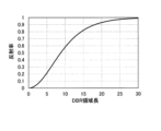
- the DBR region 13 is arranged on the light emitting side, if it is too long, the reflectance becomes high and the light cannot be efficiently emitted (cannot be extracted). Therefore, it is desirable to set the reflectance of the DBR region 13 to 5 to 50%.
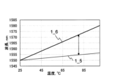
- the gain peak S113 of the MQW active layer shifts to the long wavelength side (wavelength ⁇ 1_a) and the intensity decreases.
- the oscillation wavelength due to the ring resonator 12 and the DBR diffraction grating 131 also shifts to the longer wavelength side, but the amount of shift of this wavelength ( ⁇ 1_1') is smaller than the amount of shift of the gain peak.
- a shift occurs between the gain peak ( ⁇ 1_a) of the MQW active layer and the oscillation wavelength peak ( ⁇ 1_1') (1_2 in the figure). This degrades the high temperature characteristics of this laser.
- FIG. 3 shows the calculation results of the temperature dependence of the oscillation peak wavelength and gain peak wavelength in the semiconductor laser.
- two oscillation wavelengths can be obtained by forming a uniform diffraction grating with a wider stop band width of the DFB.
- the difference between the wavelength for oscillation at room temperature and the wavelength for oscillation at high temperature is determined by the stop band width of the DFB diffraction grating.
- the DFB stopband width almost depends on the coupling coefficient of the diffraction grating.
- the two waveguides 222_1 and 222_2 are optically coupled to the ring waveguide 221, and one of the two waveguides 222_1 and 222_2 has a gain through the taper 14. Optically coupled with region 11 .
- the other waveguide 222_2 has a loop mirror 23 at one end.
- the ring waveguide 221, taper 14 and loop mirror 23 are made of InP. Other configurations are the same as those of the first embodiment.
- loop mirror 23 an example using the loop mirror 23 has been shown, but the present invention is not limited to this, and instead of the loop mirror 23, as shown in FIG. Any structure (light reflecting portion) that reflects the oscillation light emitted from the ring resonator 22 may be formed.
Landscapes
- Physics & Mathematics (AREA)
- Condensed Matter Physics & Semiconductors (AREA)
- General Physics & Mathematics (AREA)
- Electromagnetism (AREA)
- Optics & Photonics (AREA)
- Semiconductor Lasers (AREA)
Abstract
Description
本発明の第1の実施の形態について図1A~図3を参照して説明する。
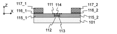
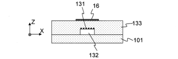
本実施の形態に係る半導体レーザは、図1Aに示すように、SiO2101上に、利得領域11と、リング共振器12と、DBR(Distributed Bragg Reflector)領域13と備える。
本実施の形態に係る半導体レーザ10の動作を、以下に説明する。
図3に、半導体レーザにおける発振ピーク波長と利得ピーク波長との温度依存性の計算結果を示す。
本発明の第2の実施の形態に係る半導体レーザについて、図4を参照して説明する。
本実施の形態に係る半導体レーザ20は、図4に示すように、SiO2101上に、利得領域11と、リング共振器22と、DBR(Distributed Bragg Reflector)領域13と、ループミラー23とを備える。
112 第1の半導体層
113 活性層
114 第2の半導体層
115_1 p型半導体層
115_2 n型半導体層
12 反射器(リング共振器)
131 回折格子
132 導波路層
16 屈折率制御部
Claims (8)
- 順に、第1の半導体層と、活性層と、第2の半導体層とを備える導波路構造と、
前記活性層の一方の側面に接して配置されるp型半導体層と、
前記活性層の他方の側面に接して配置されるn型半導体層と、
前記活性層の導波方向の一端に光学的に結合される反射器と、
前記活性層の導波方向の他端に光学的に結合される導波路層と、
前記導波路層の下面と上面とのいずれか一方に配置される回折格子と、
前記導波路層の屈折率を変化させる屈折率制御部と
を備える半導体レーザ。 - 前記反射器が複数のモードの発振光を発生させ、
前記屈折率制御部がオフの状態で、前記複数のモードの発振光のうち、所定の波長の前記発振光が、前記回折格子により選択され発振し、
前記屈折率制御部がオンの状態で、前記複数のモードの発振光のうち、所定の波長より長波長側の前記発振光が、前記回折格子により選択され発振する
ことを特徴とする請求項1に記載の半導体レーザ。 - 前記反射器が、リング共振器である
ことを特徴とする請求項1又は請求項2に記載の半導体レーザ。 - 前記リング共振器に光学的に結合するループミラーを備える
ことを特徴とする請求項3に記載の半導体レーザ。 - 前記リング共振器に光学的に結合し、一方の端部に回折格子を有する導波路を備える
ことを特徴とする請求項3に記載の半導体レーザ。 - 前記反射器が、サンプルド・グレーティングを有する導波路である
ことを特徴とする請求項1又は請求項2に記載の半導体レーザ。 - 前記屈折率制御部が、ヒータである
ことを特徴とする請求項1から請求項6のいずれか一項に記載の半導体レーザ。 - 前記屈折率制御部が、電源に接続され、前記導波路層に配置される電極であって、前記電極にバイアスを印加して、前記導波路層のキャリア密度を変化させる
ことを特徴とする請求項1から請求項6のいずれか一項に記載の半導体レーザ。
Priority Applications (3)
| Application Number | Priority Date | Filing Date | Title |
|---|---|---|---|
| JP2023568777A JP7655404B2 (ja) | 2021-12-20 | 2021-12-20 | 半導体レーザ |
| US18/721,626 US20250055254A1 (en) | 2021-12-20 | 2021-12-20 | Semiconductor Laser |
| PCT/JP2021/047031 WO2023119366A1 (ja) | 2021-12-20 | 2021-12-20 | 半導体レーザ |
Applications Claiming Priority (1)
| Application Number | Priority Date | Filing Date | Title |
|---|---|---|---|
| PCT/JP2021/047031 WO2023119366A1 (ja) | 2021-12-20 | 2021-12-20 | 半導体レーザ |
Publications (1)
| Publication Number | Publication Date |
|---|---|
| WO2023119366A1 true WO2023119366A1 (ja) | 2023-06-29 |
Family
ID=86901569
Family Applications (1)
| Application Number | Title | Priority Date | Filing Date |
|---|---|---|---|
| PCT/JP2021/047031 Ceased WO2023119366A1 (ja) | 2021-12-20 | 2021-12-20 | 半導体レーザ |
Country Status (3)
| Country | Link |
|---|---|
| US (1) | US20250055254A1 (ja) |
| JP (1) | JP7655404B2 (ja) |
| WO (1) | WO2023119366A1 (ja) |
Families Citing this family (1)
| Publication number | Priority date | Publication date | Assignee | Title |
|---|---|---|---|---|
| CN120709817B (zh) * | 2025-09-01 | 2025-11-28 | 苏州实验室 | 弯曲波导面发射半导体激光器 |
Citations (6)
| Publication number | Priority date | Publication date | Assignee | Title |
|---|---|---|---|---|
| US20100260220A1 (en) * | 2009-03-26 | 2010-10-14 | Gideon Yoffe | Semiconductor laser device and circuit for and method of driving same |
| JP2012256667A (ja) * | 2011-06-08 | 2012-12-27 | Nippon Telegr & Teleph Corp <Ntt> | 半導体レーザ光源 |
| JP2016152360A (ja) * | 2015-02-18 | 2016-08-22 | 富士通株式会社 | 光半導体装置 |
| JP2016178283A (ja) * | 2015-03-20 | 2016-10-06 | 古河電気工業株式会社 | 波長可変レーザ素子およびレーザモジュール |
| JP2017168545A (ja) * | 2016-03-15 | 2017-09-21 | 富士通株式会社 | 光モジュール |
| JP2017204601A (ja) * | 2016-05-13 | 2017-11-16 | 日本電信電話株式会社 | 半導体レーザ |
-
2021
- 2021-12-20 JP JP2023568777A patent/JP7655404B2/ja active Active
- 2021-12-20 WO PCT/JP2021/047031 patent/WO2023119366A1/ja not_active Ceased
- 2021-12-20 US US18/721,626 patent/US20250055254A1/en active Pending
Patent Citations (6)
| Publication number | Priority date | Publication date | Assignee | Title |
|---|---|---|---|---|
| US20100260220A1 (en) * | 2009-03-26 | 2010-10-14 | Gideon Yoffe | Semiconductor laser device and circuit for and method of driving same |
| JP2012256667A (ja) * | 2011-06-08 | 2012-12-27 | Nippon Telegr & Teleph Corp <Ntt> | 半導体レーザ光源 |
| JP2016152360A (ja) * | 2015-02-18 | 2016-08-22 | 富士通株式会社 | 光半導体装置 |
| JP2016178283A (ja) * | 2015-03-20 | 2016-10-06 | 古河電気工業株式会社 | 波長可変レーザ素子およびレーザモジュール |
| JP2017168545A (ja) * | 2016-03-15 | 2017-09-21 | 富士通株式会社 | 光モジュール |
| JP2017204601A (ja) * | 2016-05-13 | 2017-11-16 | 日本電信電話株式会社 | 半導体レーザ |
Non-Patent Citations (1)
| Title |
|---|
| AIHARA TAKUMA; HIRAKI TATSUROU; FUJII TAKURO; TAKEDA KOJI; KAKITSUKA TAKAAKI; TSUCHIZAWA TAI; MATSUO SHINJI: "Membrane III-V/Si DFB Laser Using Uniform Grating and Width-Modulated Si Waveguide", JOURNAL OF LIGHTWAVE TECHNOLOGY, IEEE, USA, vol. 38, no. 11, 9 March 2020 (2020-03-09), USA, pages 2961 - 2967, XP011790448, ISSN: 0733-8724, DOI: 10.1109/JLT.2020.2978808 * |
Also Published As
| Publication number | Publication date |
|---|---|
| JP7655404B2 (ja) | 2025-04-02 |
| JPWO2023119366A1 (ja) | 2023-06-29 |
| US20250055254A1 (en) | 2025-02-13 |
Similar Documents
| Publication | Publication Date | Title |
|---|---|---|
| Spott et al. | Heterogeneous integration for mid-infrared silicon photonics | |
| US8615025B2 (en) | Method and system for hybrid integration of a tunable laser | |
| US6088376A (en) | Vertical-cavity-surface-emitting semiconductor devices with fiber-coupled optical cavity | |
| US8605766B2 (en) | Method and system for hybrid integration of a tunable laser and a mach zehnder modulator | |
| US8155161B2 (en) | Semiconductor laser | |
| CN104937791B (zh) | 激光装置、光调制装置以及光半导体元件 | |
| US8787420B2 (en) | Integrated semiconductor laser element | |
| US20130235890A1 (en) | Tunable hybrid laser with carrier-induced phase control | |
| US20070133647A1 (en) | Wavelength modulated laser | |
| US8576472B2 (en) | Optoelectronic device with controlled temperature dependence of the emission wavelength and method of making same | |
| JP2016178283A (ja) | 波長可変レーザ素子およびレーザモジュール | |
| US8687665B1 (en) | Mutually injection locked lasers for enhanced frequency response | |
| JP2007005594A (ja) | 半導体光素子及びそれを用いたモジュール | |
| WO2003007444A1 (en) | Semiconductor zigzag laser and optical amplifier | |
| WO2005053124A1 (ja) | 分布帰還型半導体レーザ、分布帰還型半導体レーザアレイ及び光モジュール | |
| JP5001239B2 (ja) | 半導体波長可変レーザ | |
| WO2004030161A2 (en) | Single mode grating-outcoupled surface emitting laser with broadband and narrow-band dbr reflectors | |
| JP7655404B2 (ja) | 半導体レーザ | |
| JP5022015B2 (ja) | 半導体レーザ素子及びそれを用いた光モジュール | |
| JP7719999B2 (ja) | 半導体レーザ | |
| JP2011086714A (ja) | 波長可変レーザ | |
| KR100626270B1 (ko) | 광 대역 파장 가변 결합 링 반사기 레이저 다이오드 | |
| KR102300860B1 (ko) | 고출력 위상 천이 분포 궤환 레이저 다이오드 | |
| US20250047068A1 (en) | Distributed feedback lasers and methods for fabricating such lasers | |
| US20050226283A1 (en) | Single-mode semiconductor laser with integrated optical waveguide filter |
Legal Events
| Date | Code | Title | Description |
|---|---|---|---|
| 121 | Ep: the epo has been informed by wipo that ep was designated in this application |
Ref document number: 21968804 Country of ref document: EP Kind code of ref document: A1 |
|
| ENP | Entry into the national phase |
Ref document number: 2023568777 Country of ref document: JP Kind code of ref document: A |
|
| WWE | Wipo information: entry into national phase |
Ref document number: 18721626 Country of ref document: US |
|
| NENP | Non-entry into the national phase |
Ref country code: DE |
|
| 122 | Ep: pct application non-entry in european phase |
Ref document number: 21968804 Country of ref document: EP Kind code of ref document: A1 |