WO2023113037A1 - 蓄電デバイス用外装材の成形工程における品質管理方法、検査方法、蓄電デバイス用外装材、及び蓄電デバイスの製造方法 - Google Patents
蓄電デバイス用外装材の成形工程における品質管理方法、検査方法、蓄電デバイス用外装材、及び蓄電デバイスの製造方法 Download PDFInfo
- Publication number
- WO2023113037A1 WO2023113037A1 PCT/JP2022/046548 JP2022046548W WO2023113037A1 WO 2023113037 A1 WO2023113037 A1 WO 2023113037A1 JP 2022046548 W JP2022046548 W JP 2022046548W WO 2023113037 A1 WO2023113037 A1 WO 2023113037A1
- Authority
- WO
- WIPO (PCT)
- Prior art keywords
- storage device
- exterior material
- layer
- power storage
- electricity storage
- Prior art date
Links
Images


Classifications
-
- B—PERFORMING OPERATIONS; TRANSPORTING
- B32—LAYERED PRODUCTS
- B32B—LAYERED PRODUCTS, i.e. PRODUCTS BUILT-UP OF STRATA OF FLAT OR NON-FLAT, e.g. CELLULAR OR HONEYCOMB, FORM
- B32B3/00—Layered products comprising a layer with external or internal discontinuities or unevennesses, or a layer of non-planar form; Layered products having particular features of form
- B32B3/26—Layered products comprising a layer with external or internal discontinuities or unevennesses, or a layer of non-planar form; Layered products having particular features of form characterised by a particular shape of the outline of the cross-section of a continuous layer; characterised by a layer with cavities or internal voids ; characterised by an apertured layer
- B32B3/30—Layered products comprising a layer with external or internal discontinuities or unevennesses, or a layer of non-planar form; Layered products having particular features of form characterised by a particular shape of the outline of the cross-section of a continuous layer; characterised by a layer with cavities or internal voids ; characterised by an apertured layer characterised by a layer formed with recesses or projections, e.g. hollows, grooves, protuberances, ribs
-
- B—PERFORMING OPERATIONS; TRANSPORTING
- B32—LAYERED PRODUCTS
- B32B—LAYERED PRODUCTS, i.e. PRODUCTS BUILT-UP OF STRATA OF FLAT OR NON-FLAT, e.g. CELLULAR OR HONEYCOMB, FORM
- B32B7/00—Layered products characterised by the relation between layers; Layered products characterised by the relative orientation of features between layers, or by the relative values of a measurable parameter between layers, i.e. products comprising layers having different physical, chemical or physicochemical properties; Layered products characterised by the interconnection of layers
- B32B7/02—Physical, chemical or physicochemical properties
- B32B7/025—Electric or magnetic properties
-
- H—ELECTRICITY
- H01—ELECTRIC ELEMENTS
- H01G—CAPACITORS; CAPACITORS, RECTIFIERS, DETECTORS, SWITCHING DEVICES OR LIGHT-SENSITIVE DEVICES, OF THE ELECTROLYTIC TYPE
- H01G11/00—Hybrid capacitors, i.e. capacitors having different positive and negative electrodes; Electric double-layer [EDL] capacitors; Processes for the manufacture thereof or of parts thereof
- H01G11/78—Cases; Housings; Encapsulations; Mountings
-
- H—ELECTRICITY
- H01—ELECTRIC ELEMENTS
- H01M—PROCESSES OR MEANS, e.g. BATTERIES, FOR THE DIRECT CONVERSION OF CHEMICAL ENERGY INTO ELECTRICAL ENERGY
- H01M50/00—Constructional details or processes of manufacture of the non-active parts of electrochemical cells other than fuel cells, e.g. hybrid cells
- H01M50/10—Primary casings, jackets or wrappings of a single cell or a single battery
- H01M50/102—Primary casings, jackets or wrappings of a single cell or a single battery characterised by their shape or physical structure
- H01M50/105—Pouches or flexible bags
-
- H—ELECTRICITY
- H01—ELECTRIC ELEMENTS
- H01M—PROCESSES OR MEANS, e.g. BATTERIES, FOR THE DIRECT CONVERSION OF CHEMICAL ENERGY INTO ELECTRICAL ENERGY
- H01M50/00—Constructional details or processes of manufacture of the non-active parts of electrochemical cells other than fuel cells, e.g. hybrid cells
- H01M50/10—Primary casings, jackets or wrappings of a single cell or a single battery
- H01M50/116—Primary casings, jackets or wrappings of a single cell or a single battery characterised by the material
- H01M50/124—Primary casings, jackets or wrappings of a single cell or a single battery characterised by the material having a layered structure
- H01M50/126—Primary casings, jackets or wrappings of a single cell or a single battery characterised by the material having a layered structure comprising three or more layers
- H01M50/129—Primary casings, jackets or wrappings of a single cell or a single battery characterised by the material having a layered structure comprising three or more layers with two or more layers of only organic material
-
- H—ELECTRICITY
- H01—ELECTRIC ELEMENTS
- H01M—PROCESSES OR MEANS, e.g. BATTERIES, FOR THE DIRECT CONVERSION OF CHEMICAL ENERGY INTO ELECTRICAL ENERGY
- H01M50/00—Constructional details or processes of manufacture of the non-active parts of electrochemical cells other than fuel cells, e.g. hybrid cells
- H01M50/10—Primary casings, jackets or wrappings of a single cell or a single battery
- H01M50/131—Primary casings, jackets or wrappings of a single cell or a single battery characterised by physical properties, e.g. gas-permeability or size
-
- Y—GENERAL TAGGING OF NEW TECHNOLOGICAL DEVELOPMENTS; GENERAL TAGGING OF CROSS-SECTIONAL TECHNOLOGIES SPANNING OVER SEVERAL SECTIONS OF THE IPC; TECHNICAL SUBJECTS COVERED BY FORMER USPC CROSS-REFERENCE ART COLLECTIONS [XRACs] AND DIGESTS
- Y02—TECHNOLOGIES OR APPLICATIONS FOR MITIGATION OR ADAPTATION AGAINST CLIMATE CHANGE
- Y02E—REDUCTION OF GREENHOUSE GAS [GHG] EMISSIONS, RELATED TO ENERGY GENERATION, TRANSMISSION OR DISTRIBUTION
- Y02E60/00—Enabling technologies; Technologies with a potential or indirect contribution to GHG emissions mitigation
- Y02E60/10—Energy storage using batteries
Definitions
- the present disclosure relates to a quality control method, an inspection method, an exterior material for an electrical storage device, and a method for manufacturing an electrical storage device in a molding process of an exterior material for an electrical storage device.
- Laminates have been proposed (see Patent Document 1, for example).
- an electrical storage device exterior material generally, recesses are formed by cold molding, and electrical storage device elements such as electrodes and electrolytic solutions are arranged in the spaces formed by the recesses, and heat-sealable resin is used. By heat-sealing the layers, an electricity storage device in which the electricity storage device element is accommodated inside the exterior material for an electricity storage device can be obtained.
- the formation of the concave portion for housing the electrical storage device element forms a bent portion in the electrical storage device exterior material. Since the electrical storage device exterior material is stretched in and around the bent portion, the surface portion may be whitened.
- the exterior material for an electricity storage device may be scratched during the formation of the concave portion in the exterior material for the electricity storage device or during the processes up to that point. Therefore, there is a need for a quality control method for an exterior material for an electricity storage device having recesses formed therein.
- an object of the present disclosure is to provide a novel quality control method for an exterior material for an electricity storage device in which recesses are formed by molding.
- whitening due to molding of the exterior material for an electricity storage device leads to poor appearance of the electricity storage device, so it is subject to quality control in the molding of the exterior material for an electricity storage device.
- quality control for example, if the power storage device exterior material is colored or if the degree of whitening is large, the presence or absence of whitening can be visually confirmed.
- the bent portion forming the concave portion of the power storage device exterior material and its surroundings it was found that whitening is difficult to be confirmed visually, for example, in the bent portion forming the concave portion of the power storage device exterior material and its surroundings, but the bent portion and its surroundings (electrical storage device exterior material) can be observed with a camera. If the size of the white portion exceeds a predetermined value when an image of the curved surface or side surface of the outer surface of the material is imaged and the image is binarized, it means that very fine cracks are formed. I got it.
- the main purpose of the present disclosure is to provide a novel quality control method in the molding process of exterior materials for power storage devices.
- the inventors of the present disclosure have diligently studied to solve the above problems.
- the exterior material for the power storage device to be tested is extracted from the exterior material for the power storage device in which the recess is formed, and the surface of the exterior material for the power storage device to be tested (the inner surface and at least one of the outer surfaces, flat surfaces such as side surfaces, curved surfaces such as corners and ridges) are imaged, and recesses are formed based on the size of the area of the white portion of the binarized image.
- the present inventors have found that quality control can be performed with higher accuracy by judging whether or not an exterior material for an electricity storage device is a non-defective product, as compared with the conventional visual judgment.
- the inventors of the present disclosure have diligently studied to solve the above problems.
- the exterior material for the power storage device to be tested is extracted from the exterior material for the power storage device in which the recess is formed, and the curved surface forming the recess of the exterior material for the power storage device to be tested
- An image of the surface of the part or the surface of the side part is imaged, and based on the size of the area of the white part of the binarized image, it is determined whether the exterior material for an electricity storage device in which the recess is formed is a non-defective product.
- a quality control method in a molding process of an exterior material for an electricity storage device comprising: In the quality control method, the exterior material for an electricity storage device, which is composed of a laminate including, in order from the outside, at least a substrate layer, a barrier layer, and a heat-fusible resin layer, includes the heat-fusible resin layer.
- the exterior material for an electric storage device is molded so as to protrude from the side to the base layer side, and the heat-sealable resin layer side is formed with a recess for housing the electric storage device element, and is subject to quality control, an extracting step of extracting an exterior material for an electricity storage device to be tested from the exterior material for an electricity storage device in which the concave portion is formed; a binarized image acquisition step of capturing an image of the surface of the curved surface portion forming the recess or the surface of the side portion of the exterior material for the electrical storage device to be tested obtained in the extraction step, and acquiring a binarized image; , a determination step of determining whether or not the exterior material for an electricity storage device having the concave portion formed thereon is a non-defective product based on the size of the area of the white portion of the binarized image; comprising A quality control method in the molding process of an exterior material for an electric storage device.
- the present disclosure it is possible to provide a novel quality control method in the molding process of an exterior material for an electricity storage device. Further, according to the present disclosure, it is also possible to provide a method for manufacturing an exterior material for an electricity storage device using the quality control method.
- FIG. 2 is a schematic cross-sectional view showing an example of the laminated structure of the exterior material for an electricity storage device of the present disclosure
- FIG. 2 is a schematic cross-sectional view showing an example of the laminated structure of the exterior material for an electricity storage device of the present disclosure
- FIG. 2 is a schematic cross-sectional view showing an example of the laminated structure of the exterior material for an electricity storage device of the present disclosure
- FIG. 2 is a schematic cross-sectional view showing an example of the laminated structure of the exterior material for an electricity storage device of the present disclosure
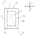
- 1 is a schematic diagram of a plain view of an exterior material for an electricity storage device of the present disclosure
- FIG. FIG. 6 is a schematic cross-sectional view taken along line A-A' in FIG. 5 (a lamination structure is omitted).
- FIG. 4 is a schematic diagram for explaining a method of housing an electricity storage device element in a package formed by the electricity storage device exterior material of the present disclosure.
- the quality control of the present disclosure is a quality control method in the molding process of an exterior material for an electricity storage device, and the quality control method includes, in order from the outside, at least a base layer, a barrier layer, a heat-sealable
- a power storage device exterior material composed of a laminate including a resin layer is molded so as to protrude from the heat-fusible resin layer side to the base layer side, and the heat-fusible resin layer side
- An electricity storage device exterior material having a recessed portion for housing an electricity storage device element is subject to quality control, and an electricity storage device exterior material to be tested is extracted from the electricity storage device exterior materials having the recessed portion formed therein.
- an extraction step a binarized image acquisition step of capturing an image of the surface of the exterior material for the power storage device to be tested obtained in the extraction step and acquiring a binarized image; and a determination step of determining whether or not the power storage device exterior material having the concave portion formed thereon is a non-defective product, based on the size of the area of the white portion of the image.
- the quality control method of the present disclosure it is possible to determine whether or not the exterior material for an electricity storage device in which the concave portion is formed is a non-defective product, based on the size of the area of the white portion of the binarized image.
- the quality control of the present disclosure is a quality control method in the molding process of an exterior material for an electricity storage device, and the quality control method includes, in order from the outside, at least a base layer, a barrier layer, a heat-sealable
- a power storage device exterior material composed of a laminate including a resin layer is molded so as to protrude from the heat-fusible resin layer side to the base layer side, and the heat-fusible resin layer side
- An electricity storage device exterior material having a recessed portion for housing an electricity storage device element is subject to quality control, and an exterior material for an electricity storage device to be tested is extracted from the exterior materials for an electricity storage device having the recessed portion formed therein.
- an extraction step and a binarization of acquiring a binarized image by imaging the surface of the curved surface portion forming the recess or the surface of the side portion of the exterior material for the power storage device to be tested obtained in the extraction step.
- an image acquisition step a determination step of determining whether or not the exterior material for an electricity storage device having the concave portion formed thereon is a non-defective product based on the size of the area of the white portion of the binarized image; characterized by comprising According to the quality control method of the present disclosure, it is possible to determine whether or not the power storage device exterior material having the concave portion formed thereon is a non-defective product based on the size of the area of the white portion of the binarized image. .
- the numerical range indicated by "-" means “more than” and “less than”.
- the notation of 2 to 15 mm means 2 mm or more and 15 mm or less.
- upper or lower limits described in a certain numerical range may be replaced with upper or lower limits of other numerical ranges described step by step.
- the upper limit and upper limit, the upper limit and lower limit, or the lower limit and lower limit, which are separately described may be combined to form a numerical range.
- upper or lower limits described in a certain numerical range may be replaced with values shown in Examples.
- the quality control method of the present disclosure is a quality control method in the process of molding an exterior material for an electric storage device.
- the power storage device exterior material to be subjected to quality control is composed of a laminate including at least a base layer, a barrier layer, and a heat-fusible resin layer in this order from the outside. ing. The lamination configuration and details of each layer of the exterior material for an electricity storage device will be described later.
- the power storage device exterior material to be quality controlled is molded so as to protrude from the heat-fusible resin layer side to the base material layer side, and the heat-fusible A concave portion in which the electricity storage device element is accommodated is formed on the resin layer side. That is, the power storage device exterior material has a recess formed by molding. As will be described later, the molding can be performed using a mold or the like.
- the shape of the concave portion formed in the power storage device exterior material is not particularly limited as long as a space capable of accommodating the power storage device element is formed.
- Specific examples of the shape of the concave portion include a substantially rectangular shape in plan view and a substantially circular shape in plan view when observed from the substrate layer 1 side.
- FIGS. 5 and 6 show schematic diagrams in which a concave portion 100 having a rectangular shape in plan view is provided in the power storage device exterior material 10 . Note that the rectangular shape in plan view includes not only a rectangular shape with right-angled corners, but also a rounded shape as shown in FIGS.
- the curved surface portion 11 includes a corner portion 11a and a ridge portion 11b protruding toward the base layer 1, and the corner portion
- Each of the 11a and the ridge line portion 11b has a predetermined radius of curvature R on the surface on the side of the base layer 1 .
- the side portion is a plane portion located between curved surface portions.
- the concave portion 100 which is rectangular in plan view, forms a rectangular parallelepiped space, and the power storage device element is accommodated in the space. If the shape of the recess is circular in plan view, the recess forms a columnar space, and the power storage device element is housed in the space.
- the size of the recess 100 is not particularly limited, and is appropriately designed according to the size of the electricity storage device (that is, the size of the electricity storage device element to be accommodated).
- the length of the long side of the recess 100 is, for example, about 20 mm or more, preferably about 30 mm. more, more preferably about 50 mm or more.
- the length of the long side of the concave portion 100 is, for example, approximately 600 mm or less, preferably approximately 400 mm or less, more preferably approximately 200 mm or less, and even more preferably approximately 100 mm or less.
- Preferred ranges for the length of the long side of the concave portion 100 are about 20 to 600 mm, about 20 to 400 mm, about 20 to 200 mm, about 20 to 100 mm, about 30 to 600 mm, about 30 to 400 mm, about 30 to 200 mm, and 30 mm. Up to about 100 mm, about 50 to 600 mm, about 50 to 400 mm, about 50 to 200 mm, and about 50 to 100 mm.
- the length of the short side of the concave portion 100 is, for example, about 10 mm or more, preferably about 20 mm or more, and more preferably about 30 mm or more.
- the length of the short side of the concave portion 100 is, for example, approximately 300 mm or less, preferably approximately 200 mm or less, more preferably approximately 100 mm or less, and even more preferably approximately 50 mm or less.
- Preferred ranges for the length of the short side of the concave portion 100 are about 10 to 300 mm, about 10 to 200 mm, about 10 to 100 mm, about 10 to 50 mm, about 20 to 300 mm, about 20 to 200 mm, about 20 to 100 mm, and 20 mm. Up to about 50 mm, about 30 to 300 mm, about 30 to 200 mm, about 30 to 100 mm, and about 30 to 50 mm.
- the length of the long side and the length of the short side of the recess 100 may be the same (that is, the shape of the recess 100 may be square in plan view).
- the depth D (see FIG. 6) of the recess 100 is not particularly limited, and is appropriately designed according to the size of the electricity storage device (that is, the size of the electricity storage device element to be accommodated).
- the thickness is about 2 to 15 mm, preferably about 4 to 10 mm.
- the concave portion 100 included in the power storage device exterior material 10 is formed by molding a film-like power storage device exterior material. Specifically, a mold (female mold) arranged on the base material layer 1 side of the laminate constituting the exterior material for the electric storage device, and a mold (male mold) arranged on the heat-fusible resin layer 4 side ), the laminate is molded (generally cold-molded) so as to protrude from the heat-fusible resin layer 4 side to the substrate layer 1 side, so that the heat-fusible resin layer 4 side A recess 100 can be formed in which the electrical storage device element is accommodated.
- the quality control method of the present disclosure includes an extraction step of extracting the exterior material for the power storage device to be tested from the exterior material for the power storage device in which the recess is formed, and the exterior material for the power storage device to be tested obtained in the extraction step.
- the surface of the portion forming the recess of the exterior material for the power storage device to be tested obtained in the extraction step preferably a surface including at least one surface
- a binarized image hereinafter sometimes referred to as a binarized image
- the power storage device exterior material to be tested is extracted from the power storage device exterior material 10 in which the recess 100 is formed (that is, the power storage device exterior material 10 in which the recess 100 is formed is used as the test subject Select and extract an arbitrary exterior material for an electricity storage device).
- the exterior material for the electricity storage device to be tested may be extracted at random, or may be extracted at a predetermined ratio (for example, 1,000 to 10,000 exterior materials for power storage devices are extracted as exterior materials for power storage devices to be tested), or all exterior materials for power storage devices in which recesses are formed may be extracted as the exterior material for the electrical storage device to be tested.
- the binary image acquisition step and the judgment step following the extraction step are performed. It is desirable to automate it and incorporate it into the production line.
- the surface of the exterior material for the power storage device to be tested obtained in the extraction step (particularly, the surface including at least one of the curved surface portion and the side surface portion forming the recess) is imaged, and two Get the valued image.
- the bent portions are formed in the exterior material for an electricity storage device by forming the recesses for accommodating the electricity storage device elements.
- the power storage device exterior material is stretched by molding, whitening may occur on the surface portion.
- whitening may occur on the surface portion of the side surface sandwiched between the bent portions.
- Whitening due to the molding of the exterior material for an electricity storage device leads to poor appearance of the electricity storage device, and is therefore subject to quality control in the molding of the exterior material for the electricity storage device. In the quality control, for example, if the power storage device exterior material is colored or if the degree of whitening is large, the presence or absence of whitening can be visually confirmed.
- the bent portion (the power storage device exterior When observing the curved surface or side surface of the material, very fine cracks may be formed.
- the conventional visual inspection has problems such as large individual differences and variations, and difficulty in judging non-defective products that are whitened to the extent that they do not affect quality. Therefore, it is desired to further improve the accuracy of the quality control method in the molding process of the exterior material for an electric storage device.
- the surface of the curved surface portion of the recess (at least one of the outer surface and the inner surface) and the surface of the side surface of the recess (outer surface and inner surface) formed by molding the exterior material for the power storage device At least one of the surfaces) is imaged, a binarized image is acquired, and based on the area (pixel) of the white part, cracks that affect the quality are formed on the curved surface or side surface to some extent. It is possible to suitably detect the quality such as whether or not the Therefore, if the quality control method of the present disclosure is used to manufacture an electricity storage device, the evaluation criteria for the area size of the white portion of the binarized image can be appropriately set according to the quality required for the electricity storage device. Therefore, it is possible to suitably suppress the production of defective products in the step of molding the exterior material for an electric storage device.
- the layer located mainly on the outside of the exterior material for an electricity storage device It is possible to suitably evaluate whether or not cracks are formed in the curved surface portion of (surface coating layer, base material layer, etc.).
- the layer thermal It is possible to suitably evaluate whether or not cracks are formed in the curved surface portion of the adhesive resin layer, adhesive layer, etc.).
- the image when a binarized image is obtained for the outer surface of the side surface of the recess formed by molding the power storage device exterior material, and the determination step is performed, the image is mainly located outside the power storage device exterior material. It is possible to suitably evaluate whether or not cracks are formed on the side surface of the layer (surface coating layer, base material layer, etc.). In addition, when a binarized image is obtained for the inner surface of the side surface of the recess formed by molding the power storage device exterior material and the determination step is performed, the layer (thermal It is possible to suitably evaluate whether or not cracks are formed on the side surface of the adhesive resin layer, adhesive layer, etc.).
- the side on which the barrier layer can be imaged i.e., the side of the barrier layer
- a binarized image is obtained on the surface of the layer laminated thereon (the side on which the layer is transparent), and a judgment step is performed to evaluate whether or not cracks are formed on the curved surface portion or side surface portion of the barrier layer. It can be done suitably.
- the imaging conditions and image binarization processing conditions in the binarized image acquisition process are not particularly limited, as long as the determination process described later can be performed appropriately. Therefore, the imaging conditions and the image binarization processing conditions can be set by appropriately combining known conditions employed as the conditions for acquiring a binarized image.
- a commercially available camera can be used as imaging equipment.
- illumination for imaging and examples of the illumination include multispectral illumination.
- the light source is not limited, blue light is preferable because short-wavelength light is easily diffused and easily detected.
- There is no particular limit on the lower limit of the threshold but if the lower limit of the threshold is lowered, the whitened area will relatively increase and it will be easier to detect.
- the evaluation criteria for the area of the white portion in the binarized image can be appropriately set according to the quality required of the electricity storage device. For example, from the viewpoint of managing whitening on the curved surface portion 11 or the side surface portion 15, the criterion for determining that the power storage device exterior material in which the concave portion is formed is a non-defective product is the upper limit of the area of the white portion ( determined upper limit).
- the criteria are preferably about 25000 pixels or less, more preferably about 20000 pixels or less, more preferably about 10000 pixels or less, even more preferably about 5000 pixels or less, even more preferably about 3000 pixels or less, even more preferably about 1000 pixels or less , more preferably about 800 pixels or less, more preferably about 500 pixels or less, more preferably about 100 pixels or less, and even more preferably about 60 pixels or less.
- the lower limit of the standard includes, for example, approximately 0 pixels or more, approximately 10 pixels or more, approximately 100 pixels or more, approximately 500 pixels or more, and approximately 5000 pixels or more. For example, in applications where the control of whitening is very stringent, it is preferable to reduce the value of the upper limit of the criterion.
- the criterion is, for example, about 5000 pixels or less, more preferably about 3000 pixels or less, more preferably about 1000 pixels or less, more preferably about 800 pixels or less, more preferably about 500 pixels or less, more preferably Preferably, the reference is set at about 100 pixels or less, more preferably about 60 pixels or less.
- the criteria for determining that the power storage device exterior material having the concave portion is non-defective are, for example, the range of the area of the white portion in the binarized image, for example, about 0 to 25000 pixels, about 0 to 20000 pixels, 0-10000 pixels, 0-5000 pixels, 0-3000 pixels, 0-1000 pixels, 0-800 pixels, 0-500 pixels, 0-100 pixels, 0-60 pixels, 10- About 25000 pixels, about 10-20000 pixels, about 10-10000 pixels, about 10-5000 pixels, about 10-3000 pixels, about 10-1000 pixels, about 10-800 pixels, about 10-500 pixels, 10-100 pixels about 10 to 60 pixels, about 100 to 25,000 pixels, about 100 to 20,000 pixels, about 100 to 10,000 pixels, about 100 to 5,000 pixels, about 100 to 3,000 pixels, about 100 to 1,000 pixels, about 100 to 800 pixels, About
- the curved surface portion 11 of the outer surface of the base material layer 1 side forming the concave portion 100 of the power storage device exterior material 10 The curved surface portion 11 protruding toward the base material layer 1 was photographed under the following conditions, and the binarized image was obtained.
- the camera is a 5-megapixel black-and-white camera (for example, Keyence model number CA-H500MX), the lens (for example, Keyence model number CA-LM0510), and the lighting is multispectral lighting (for example, Keyence model number CA -DRM10X).
- the light source is blue
- the binarization threshold is 75 to 255
- the shutter speed is 1/30 (s) (adjusted in the range of 1/50000 (s) to 1/15 (s))
- the camera sensitivity is 1.0 to It is adjusted in the range of 7.0
- the lighting output is adjusted in the range of 0 to 511W.
- Conditions for the side surface portion 15 can be similarly set.
- the imaging conditions and the image binarization processing conditions in the binarized image acquisition step are not particularly limited as long as the determination step described later can be performed appropriately.
- the bending part is subject to the greatest strain and cracks are likely to occur.
- a crack is generated in a layer that constitutes an exterior material for an electricity storage device, such as a surface coating layer, a gap is generated, and when an image of the surface captured by a camera is binarized, the area of the portion recognized as white increases.
- the exterior material for an electricity storage device has excellent electrolyte resistance, if cracks occur on the curved surface or side surface formed by molding, the electrolyte will permeate through the cracks and the exterior material will peel off (exterior It leads to peeling between the layers that make up the material).
- the hard exterior material for energy storage devices cannot follow the molding and cracks occur. It is preferable to adjust by making it flexible and elastic.
- the exterior material for an electricity storage device is hard and flexible, if there are many additives such as wax and particles, the adhesion between the resin and particles or between the resin and wax is weak, and cracks are likely to occur at the boundaries. Therefore, it is preferable to adjust the content of the additive to the necessary minimum.
- the curved surface portion 11 that is the object of acquisition of the binarized image is the portion that is most stretched by molding (molding in the formation of the concave portion 100) (i.e., cracks are most likely to occur). easy part).
- the most stretched portion is the portion where the area of the white portion is the largest, and the portion where the area of the white portion of the curved surface portion 11 is the largest.
- the corners 11a are present at four locations in the shape of the mold for molding.
- the ridgeline portion 11b may be the most stretched portion.
- the curvature radius R of the ridgeline portion 11b is smaller than the curvature radius R of the corner portion 11a on the surface on the base layer 1 side described above, the curved portion 11 protrudes toward the base layer 1 side.
- the ridgeline portion 11b that is located can be the portion that is most stretched. In such a case, it is preferable to set the ridgeline portion 11b as a target for acquiring the binarized image.
- the ridgeline portion is taken as the acquisition target of the binarized image.
- the curved surface portion 13 in FIG. 6 is a curved surface portion that does not protrude toward the base layer 1 side. It may or may not be adopted as the curved surface portion 11 which is small and is the object of acquisition of the binarized image.
- the side surface portion 15 located between the curved surface portion 11 and the curved surface portion 13 in FIG. 6 can also be employed as the curved surface portion 11 for which the binarized image is to be obtained. This is because the side surface portion 15 is also a position where whitening is likely to occur due to stretching.
- the corner portions 11a and the ridge portions 11b on the side of the heat-fusible resin layer 4 may also be compressed by molding and cracks may be formed.
- the quality control method of the present disclosure by applying the binary image acquisition step to the inner surface of the curved surface portion forming the concave portion of the exterior material for an electric storage device, For the layer 4 side as well, a binarized image can be obtained and the determination process can be performed. Whether cracks are formed in the curved surface portion of the heat-fusible resin layer 4 may be evaluated for either the corner portion 11a or the ridgeline portion 11b, but it is preferable to perform the evaluation for the ridgeline portion 11b.
- a portion that is most whitened as a result of visual evaluation of appearance is suitable as a target portion for obtaining a binarized image.
- the side surface portion 15 although it varies depending on the size of the concave portion, for example, 50%, 30%, and 20% of the molding depth from the curved surface portion 11 (ridgeline portion 11b) in FIG. , 15%, 10%, or 5%, or 5 mm, 3 mm, 2 mm, 1 mm, 0.5 mm, or 0.1 mm.
- the power storage device exterior material 10 is colored (specifically, at least one layer (for example, By coloring the base material layer 1, the adhesive layer 2, the colored layer, the surface coating layer 6, etc., which will be described later, when the power storage device exterior material 10 is observed from the base material layer 1 side, the barrier layer 3 When a different color is visually recognized), the whitening of the curved surface portion 11 or the side surface portion 15 is likely to be determined as a defective product.
- the quality control method of the present disclosure is preferably used.
- the outermost layer of the power storage device exterior material 10 for example, the base material described later.
- the composition and thickness of the material layer 1, the surface coating layer 6, etc.), the shape, size, surface roughness of the mold, and the pressing pressure of the mold are adjusted to obtain a predetermined value. adjust. Further, as will be described later, the area of the white portion may be adjusted by adjusting the lamination conditions of each layer in the step of laminating the power storage device exterior material 10 .
- the surface of the power storage device exterior material in the step of molding the power storage device exterior material, the surface of the power storage device exterior material (particularly preferably, the surface including at least one of the curved surface portion and the side surface portion forming the recess)
- a novel quality control method comprising a determination step of determining whether or not an exterior material for an electricity storage device having recesses formed therein is a non-defective product, based on the size of the area of the white portion of the binarized image of It is also possible to perform more accurate quality control than conventional visual quality control. Therefore, by using the quality control method of the present disclosure for manufacturing power storage devices, it becomes possible to manufacture non-defective power storage devices more efficiently.
- the determination step is based on whether or not the power storage device exterior material has cracks that affect the quality to some extent in the layers constituting the power storage device exterior material due to molding when forming the recess. It can be used as a determination method for evaluating the characteristics (molding characteristics) of exterior materials for devices. It can be easily evaluated.
- a method for manufacturing an electricity storage device comprises a laminate having at least a base layer 1, a barrier layer 3, and a heat-fusible resin layer 4 in this order from the outside.
- the power storage device element is sealed with a packaging body formed by heat-sealing the heat-sealable resin layer 4 at the peripheral edge of the power storage device exterior material 10 (for example, the peripheral edge portion 14 in FIGS. 5 and 6).
- the method for manufacturing an electricity storage device according to the present disclosure uses the quality control method described in the section “1. Quality control method” for manufacturing an electricity storage device, and redundant descriptions will be omitted as appropriate. Further, as described above, the lamination structure of the exterior material for an electric storage device and the details of each layer will be described later.
- the electricity storage device exterior is formed with a concave portion for housing an electricity storage device element so as to protrude from the heat-sealable resin layer side of the electricity storage device exterior material toward the base layer side. It has a process of preparing materials.
- the exterior material for an electricity storage device in which such recesses are formed is as described in the section "1. Quality control method" above, and the description is omitted.
- an extraction step of extracting the exterior material for the electricity storage device to be tested from the exterior material for the electricity storage device in which the recess is formed, and the electricity storage to be tested obtained in the extraction step A binarized image acquisition step of capturing an image of the surface of the device exterior material (particularly preferably, the surface including at least one of the curved surface portion and the side surface portion forming the recess) and acquiring a binarized image; and a determination step of determining whether or not the power storage device exterior material having the concave portion formed thereon is a non-defective product, based on the size of the area of the white portion of the processed image.
- a method for manufacturing an electricity storage device includes a step of housing an electricity storage device element in a concave portion of an exterior material for an electricity storage device to manufacture an electricity storage device.
- the method for manufacturing an electricity storage device of the present disclosure when it is determined that the exterior material for an electricity storage device in which the recess is formed is non-defective as a result of the determination step, it is determined that the formation of the recess is appropriate.
- An electricity storage device is manufactured by housing an electricity storage device element in the .
- the evaluation criteria for the area of the white portion can be appropriately set according to the quality required for the electricity storage device.
- the area of the white portion of the binarized image of the surface of the portion 11 or the side portion 15 is preferably about 20000 pixels or less, more preferably about 10000 pixels or less, More preferably about 5000 pixels or less, more preferably about 3000 pixels or less. From this point of view, preferable ranges for the area of the white portion in the binarized image include about 0 to 20,000 pixels, about 0 to 10,000 pixels, about 0 to 5,000 pixels, and about 0 to 3,000 pixels.
- a known method can be applied to the method of housing the electricity storage device element in the concave portion 100 and manufacturing the electricity storage device. Specifically, an electrode, an electrolytic solution, and the like constituting the electricity storage device element are accommodated in the recess 100, and the heat-sealable resin layers 4 of the exterior material 10 for the electricity storage device are heat-sealed to each other, thereby forming the electricity storage device element. It seals and obtains an electrical storage device.
- the inspection method of the present disclosure is a method for inspecting an exterior material for a power storage device having recesses formed therein.
- the exterior material for an electricity storage device which is composed of a laminate including, in order from the outside, at least a base material layer, a barrier layer, and a heat-fusible resin layer, includes the heat-fusible resin
- An electric storage device exterior material is to be inspected, which is molded so as to protrude from the layer side to the base layer side, and in which a concave portion for housing an electric storage device element is formed on the heat-fusible resin layer side.
- the above-described quality control method of the present disclosure can be said to be a quality control method using the inspection method of the present disclosure, and descriptions of matters overlapping with the items described in the section "1. Quality control method" will be omitted as appropriate. Further, as described above, the lamination structure of the exterior material for an electric storage device and the details of each layer will be described later.
- the power storage device exterior material having the concave portion to be inspected is as described in the section "1. Quality control method" above, and the description is omitted.
- the surface of the power storage device exterior material (particularly preferably, the surface including at least one of the curved surface portion and the side surface portion forming the recess) is imaged, and the binarized image is obtained.
- Determination to determine whether or not the power storage device exterior material having the concave portion formed therein is a non-defective product based on the binary image acquisition step to be acquired and the size of the area of the white portion of the binarized image. It has a process.
- the binarized image acquisition process and the determination process are also the same as described in the section "1. Quality control method", and the description will be omitted.
- the evaluation criteria for the area of the white portion can be appropriately set according to the quality required for the electricity storage device.
- the area of the white portion of the binarized image of the surface of the portion 11 or the side portion 15 is preferably about 20000 pixels or less, more preferably about 10000 pixels or less, More preferably, it is about 5000 pixels or less, more preferably about 3000 pixels or less. From this point of view, preferable ranges for the area of the white portion in the binarized image include about 0 to 20,000 pixels, about 0 to 10,000 pixels, about 0 to 5,000 pixels, and about 0 to 3,000 pixels.
- the exterior material 10 for an electricity storage device of the present disclosure is an electricity storage device composed of a laminate including at least a base material layer 1 , a barrier layer 3 , and a heat-fusible resin layer 4 in this order from the outside. It is an exterior material for devices.
- the power storage device exterior material 10 is molded so as to protrude from the heat-fusible resin layer 4 side to the base layer 1 side, and the heat-fusible resin layer 4 side has a concave portion 100 in which the power storage device element is accommodated.
- the surface of the power storage device exterior material (particularly preferably, the surface including at least one of the curved surface portion and the side surface portion forming the recess) is imaged, and the size of the area of the white portion of the binarized image is It is characterized by being 20000 pixels or less. That is, the power storage device exterior material 10 of the present disclosure is obtained by imaging the surface of the curved surface portion 11 or the side surface portion 15 of the power storage device exterior material 10 described in "1. Quality Control Method" above. The size of the area of the white portion of the converted image is 20000 pixels or less. Therefore, description of the shape and the like of the power storage device exterior material 10 is omitted.
- the electrolytic solution may be removed from the electricity storage device exterior material during the manufacturing process of the electricity storage device. When it adheres to the surface of the electric storage device, the electrolytic solution may permeate the cracks and peel off between the layers constituting the exterior material for an electricity storage device.
- the area of the white portion of the binarized image of the curved surface portion 11 or the side surface portion 15 of the electric storage device exterior material 10 in which the concave portion is formed is set to a low value of 20000 pixels or less, and the area is preferably is about 10,000 pixels or less, more preferably about 5,000 pixels or less, and more preferably about 3,000 pixels or less. It is about 0 to 3000 pixels.
- the preferable area of the white portion of the curved surface portion 11, the acquisition method of the binarized image, and the details of the acquisition location are as described in the above "1. Quality Control Method".
- the power storage device exterior material 10 before forming the recess 100 is arranged so that the power storage device exterior material 10 protrudes from the heat-fusible resin layer 4 side to the base layer 1 side.
- a concave portion 100 in which an electricity storage device element is accommodated on the heat-fusible resin layer 4 side, and the surface of the curved surface portion 11 or the side portion 15 that forms the concave portion 100 of the electricity storage device exterior material 10 and the area size of the white portion of the binarized image is about 20000 pixels or less, preferably about 10000 pixels or less, more preferably about 5000 pixels or less, further preferably about 3000 pixels or less.
- the preferred range of the area is about 0 to 20000 pixels, about 0 to 10000 pixels, about 0 to 5000 pixels, and about 0 to 3000 pixels.
- the electric storage device exterior material 10 is not formed with the recesses 100 described above, and when the recesses are formed under predetermined molding conditions, the area of the white portion is 20000 pixels or less.
- molding condition Between a molding die (female mold) having a diameter of 54.5 mm (TD) x 31.6 mm (MD) and a corresponding molding die (male mold), an exterior material for an electric storage device is placed, and the female mold side is It is arranged so as to be on the base material layer side, and cold forming is performed with a pressing pressure (surface pressure) of 0.25 MPa and a forming depth of 3.0 mm to form a concave portion having a rectangular shape in plan view.
- the clearance between the female and male molds is 0.5 mm.
- the surface of the female mold has a maximum height roughness (nominal value of Rz) of 0.8 ⁇ m as specified in Table 2 of JIS B 0659-1: 2002 Annex 1 (Reference) Comparative Surface Roughness Standard Piece .
- the corner R of the female mold is 2.0 mm and the ridge R is 2.5 mm.
- the surface of the male mold has a maximum height roughness (nominal value of Rz) of 3.2 ⁇ m as specified in Table 2 of JIS B 0659-1: 2002 Annex 1 (reference) Comparative surface roughness standard piece .
- the corner R of the male mold is 2.0 mm and the ridge R is 2.0 mm.
- the male corner R and ridge R are specified in JIS B 0659-1: 2002 Annex 1 (reference) Table 2 of the surface roughness standard piece for comparison, the maximum height roughness (nominal value of Rz) is 1 .6 ⁇ m. Even if the molding depth of 3.0 mm is changed to 6.5 mm, or even 7.5 mm, it is more preferable that the area size of the white portion of the binarized image satisfies the above value.
- the exterior material 10 for an electricity storage device is, for example, as shown in FIG. It is configured.
- the base material layer 1 is the outermost layer
- the heat-fusible resin layer 4 is the innermost layer.
- the heat-sealable resin layers 4 of the electricity storage device exterior material 10 are opposed to each other, and the peripheral edge portion 14 is heat-sealed.
- a power storage device element is accommodated in the space formed by the above.
- the barrier layer 3 is the reference, the heat-fusible resin layer 4 side is inner than the barrier layer 3, and the base layer 1 side is more than the barrier layer 3. outside.
- the electrical storage device exterior material 10 is provided between the base material layer 1 and the barrier layer 3 for the purpose of improving the adhesion between these layers, if necessary. It may have an adhesive layer 2 .
- an adhesive layer 5 may optionally be provided between the barrier layer 3 and the heat-fusible resin layer 4 for the purpose of enhancing the adhesion between these layers.
- a surface coating layer 6 or the like may be provided on the outside of the base material layer 1 (the side opposite to the heat-fusible resin layer 4 side), if necessary.
- the thickness of the laminate constituting the power storage device exterior material 10 is not particularly limited. Hereafter, about 120 micrometers or less are mentioned.
- the thickness of the laminate constituting the power storage device exterior material 10 is preferably about 35 ⁇ m or more, about 45 ⁇ m or more, about 60 ⁇ m or more can be mentioned.
- the preferred range of the laminate constituting the power storage device exterior material 10 is, for example, about 35 to 210 ⁇ m, about 35 to 190 ⁇ m, about 35 to 180 ⁇ m, about 35 to 155 ⁇ m, about 35 to 120 ⁇ m, and about 45 to 210 ⁇ m.
- the thickness is preferably about 60 to 155 ⁇ m when making the electricity storage device lighter and thinner, and about 155 to 190 ⁇ m when improving moldability.
- the thickness (total thickness) of the laminate constituting the power storage device exterior material 10 is the base layer 1, the adhesive layer 2 provided as necessary, the barrier layer 3, if necessary
- the ratio of the total thickness of the adhesive layer 5, the heat-fusible resin layer 4, and the surface coating layer 6 provided as necessary is preferably 90% or more, more preferably 95% or more, More preferably, it is 98% or more.
- the electrical storage device exterior material 10 of the present disclosure includes the base material layer 1, the adhesive layer 2, the barrier layer 3, the adhesive layer 5, and the heat-fusible resin layer 4, the electrical storage device exterior
- the ratio of the total thickness of each layer to the thickness (total thickness) of the laminate constituting the material 10 is preferably 90% or more, more preferably 95% or more, and still more preferably 98% or more.
- the power storage device exterior material 10 of the present disclosure is a laminate including the base material layer 1, the adhesive layer 2, the barrier layer 3, and the heat-fusible resin layer 4, the power storage device exterior material
- the ratio of the total thickness of each layer to the thickness (total thickness) of the laminate constituting 10 is, for example, 80% or more, preferably 90% or more, more preferably 95% or more, and further preferably 98% or more. can be done.
- the base material layer 1 is a layer provided for the purpose of exhibiting a function as a base material of an exterior material for an electric storage device.
- the base material layer 1 is located on the outer layer side of the exterior material for electrical storage devices.
- the material forming the base material layer 1 is not particularly limited as long as it functions as a base material, that is, at least has insulating properties.
- the base material layer 1 can be formed using, for example, a resin, and the resin may contain additives described later.
- the base material layer 1 can be made of, for example, a resin film.
- the base material layer 1 is formed of a resin film
- the resin forming the base material layer 1 may be formed into a film on the surface of the barrier layer 3 or the like by extrusion molding or coating to form the base material layer 1 formed of a resin film.
- the resin film may be an unstretched film or a stretched film. Examples of stretched films include uniaxially stretched films and biaxially stretched films, with biaxially stretched films being preferred. Examples of stretching methods for forming a biaxially stretched film include successive biaxial stretching, inflation, and simultaneous biaxial stretching. Methods for applying the resin include a roll coating method, a gravure coating method, an extrusion coating method, and the like.
- resins forming the base material layer 1 include resins such as polyester, polyamide, polyolefin, epoxy resin, acrylic resin, fluororesin, polyurethane, silicon resin, phenolic resin, and modified products of these resins. Further, the resin forming the base material layer 1 may be a copolymer of these resins or a modified product of the copolymer. Furthermore, it may be a mixture of these resins.
- the base material layer 1 preferably contains these resins as a main component, and more preferably contains polyester or polyamide as a main component.
- the main component means that the resin component contained in the base layer 1 has a content of, for example, 50% by mass or more, preferably 60% by mass or more, more preferably 70% by mass or more, and further preferably 80% by mass. % or more, more preferably 90 mass % or more, more preferably 95 mass % or more, still more preferably 98 mass % or more, still more preferably 99 mass % or more.
- the base material layer 1 contains polyester or polyamide as a main component means that the content of polyester or polyamide among the resin components contained in the base material layer 1 is, for example, 50% by mass or more, preferably 60% by mass. % or more, more preferably 70 mass % or more, still more preferably 80 mass % or more, still more preferably 90 mass % or more, still more preferably 95 mass % or more, still more preferably 98 mass % or more, still more preferably 99 mass % or more means that
- polyesters and polyamides are preferred as resins forming the base material layer 1 .
- polyester examples include polyethylene terephthalate, polybutylene terephthalate, polyethylene naphthalate, polybutylene naphthalate, polyethylene isophthalate, and copolymerized polyester.
- copolyester examples include copolyester having ethylene terephthalate as a main repeating unit.
- copolymer polyester polymerized with ethylene isophthalate with ethylene terephthalate as the main repeating unit hereinafter abbreviated after polyethylene (terephthalate / isophthalate)
- polyethylene (terephthalate / adipate) polyethylene (terephthalate / sodium sulfoisophthalate)
- polyethylene (terephthalate/sodium isophthalate) polyethylene (terephthalate/phenyl-dicarboxylate), polyethylene (terephthalate/decanedicarboxylate), and the like.
- These polyesters may be used singly or in combination of two or more.
- polyamide specifically, aliphatic polyamide such as nylon 6, nylon 66, nylon 610, nylon 12, nylon 46, copolymer of nylon 6 and nylon 66; terephthalic acid and / or isophthalic acid Hexamethylenediamine-isophthalic acid-terephthalic acid copolymer polyamide such as nylon 6I, nylon 6T, nylon 6IT, nylon 6I6T (I represents isophthalic acid, T represents terephthalic acid) containing structural units derived from, polyamide MXD6 (polymetallic Polyamides containing aromatics such as silylene adipamide); alicyclic polyamides such as polyamide PACM6 (polybis(4-aminocyclohexyl)methane adipamide); Copolymerized polyamides, polyesteramide copolymers and polyetheresteramide copolymers which are copolymers of copolymerized polyamides with polyesters or polyalkylene ether glycols; and polyamides such
- the substrate layer 1 preferably includes at least one of a polyester film, a polyamide film, and a polyolefin film, preferably includes at least one of an oriented polyester film, an oriented polyamide film, and an oriented polyolefin film, More preferably, at least one of oriented polyethylene terephthalate film, oriented polybutylene terephthalate film, oriented nylon film and oriented polypropylene film is included, biaxially oriented polyethylene terephthalate film, biaxially oriented polybutylene terephthalate film and biaxially oriented nylon film. , biaxially oriented polypropylene film.
- the base material layer 1 may be a single layer, or may be composed of two or more layers.
- the substrate layer 1 may be a laminate obtained by laminating resin films with an adhesive or the like, or may be formed by co-extrusion of resin to form two or more layers. It may also be a laminate of resin films. A laminate of two or more resin films formed by coextrusion of resin may be used as the base material layer 1 without being stretched, or may be used as the base material layer 1 by being uniaxially or biaxially stretched.
- the laminate of two or more resin films in the substrate layer 1 include a laminate of a polyester film and a nylon film, a laminate of nylon films of two or more layers, and a laminate of polyester films of two or more layers. etc., preferably a laminate of a stretched nylon film and a stretched polyester film, a laminate of two or more layers of stretched nylon films, and a laminate of two or more layers of stretched polyester films.
- the substrate layer 1 is a laminate of two layers of resin films, a laminate of polyester resin films and polyester resin films, a laminate of polyamide resin films and polyamide resin films, or a laminate of polyester resin films and polyamide resin films.
- a laminate is preferred, and a laminate of polyethylene terephthalate film and polyethylene terephthalate film, a laminate of nylon film and nylon film, or a laminate of polyethylene terephthalate film and nylon film is more preferred.
- the polyester resin is resistant to discoloration when, for example, an electrolytic solution adheres to the surface. It is preferably located in the outermost layer.
- the two or more layers of resin films may be laminated via an adhesive.
- Preferred adhesives are the same as those exemplified for the adhesive layer 2 described later.
- the method for laminating two or more layers of resin films is not particularly limited, and known methods can be employed. Examples thereof include dry lamination, sandwich lamination, extrusion lamination, thermal lamination, and the like. A lamination method is mentioned. When laminating by a dry lamination method, it is preferable to use a polyurethane adhesive as the adhesive. At this time, the thickness of the adhesive is, for example, about 2 to 5 ⁇ m.
- an anchor coat layer may be formed on the resin film and laminated. Examples of the anchor coat layer include the same adhesives as those exemplified for the adhesive layer 2 described later. At this time, the thickness of the anchor coat layer is, for example, about 0.01 to 1.0 ⁇ m.
- At least one of the surface and the inside of the substrate layer 1 may contain additives such as lubricants, flame retardants, antiblocking agents, antioxidants, light stabilizers, tackifiers, and antistatic agents. good. Only one type of additive may be used, or two or more types may be mixed and used.
- the surface and the inside of the base material layer 1 contains a lubricant.
- the lubricant is not particularly limited, but preferably includes an amide-based lubricant.
- Specific examples of amide lubricants include saturated fatty acid amides, unsaturated fatty acid amides, substituted amides, methylolamides, saturated fatty acid bisamides, unsaturated fatty acid bisamides, fatty acid ester amides, and aromatic bisamides.
- saturated fatty acid amides include lauric acid amide, palmitic acid amide, stearic acid amide, behenic acid amide, and hydroxystearic acid amide.
- unsaturated fatty acid amides include oleic acid amide and erucic acid amide.
- substituted amides include N-oleyl palmitic acid amide, N-stearyl stearic acid amide, N-stearyl oleic acid amide, N-oleyl stearic acid amide, N-stearyl erucic acid amide and the like.
- methylolamide include methylol stearamide.
- saturated fatty acid bisamides include methylenebisstearic acid amide, ethylenebiscapric acid amide, ethylenebislauric acid amide, ethylenebisstearic acid amide, ethylenebishydroxystearic acid amide, ethylenebisbehenic acid amide, hexamethylenebisstearin. acid amide, hexamethylenebisbehenamide, hexamethylenehydroxystearic acid amide, N,N'-distearyladipic acid amide, N,N'-distearylsebacic acid amide and the like.
- unsaturated fatty acid bisamides include ethylenebisoleic acid amide, ethylenebiserucic acid amide, hexamethylenebisoleic acid amide, N,N'-dioleyladipic acid amide, and N,N'-dioleylsebacic acid amide. etc.
- fatty acid ester amides include stearamide ethyl stearate.
- aromatic bisamide include m-xylylenebisstearic acid amide, m-xylylenebishydroxystearic acid amide, N,N'-distearyl isophthalic acid amide and the like.
- the lubricants may be used singly or in combination of two or more, preferably in combination of two or more.
- the amount of the lubricant is not particularly limited, but is, for example, about 3 mg/m 2 or more, preferably about 4 mg/m 2 or more, and about 5 mg/m 2 or more.
- the amount of lubricant present on the surface of the substrate layer 1 is, for example, about 15 mg/m 2 or less, preferably about 14 mg/m 2 or less, and about 10 mg/m 2 or less.
- the preferred range of the amount of lubricant present on the surface of the base material layer 1 is about 3 to 15 mg/m 2 , about 3 to 14 mg/m 2 , about 3 to 10 mg/m 2 , and about 4 to 15 mg/m 2 . , about 4 to 14 mg/m 2 , about 4 to 10 mg/m 2 , about 5 to 15 mg/m 2 , about 5 to 14 mg/m 2 , and about 5 to 10 mg/m 2 .
- the lubricant present on the surface of the substrate layer 1 may be obtained by exuding the lubricant contained in the resin constituting the substrate layer 1, or by coating the surface of the substrate layer 1 with the lubricant.
- the thickness of the base material layer 1 is not particularly limited as long as it functions as a base material.
- the thickness of the base layer 1 is, for example, about 50 ⁇ m or less, preferably about 35 ⁇ m or less, 11 ⁇ m or less, and 8 ⁇ m or less.
- the preferable range of the thickness of the base material layer 1 is about 3 to 50 ⁇ m, about 3 to 35 ⁇ m, about 3 to 11 ⁇ m, about 3 to 8 ⁇ m, about 10 to 50 ⁇ m, and about 10 to 35 ⁇ m. is preferably about 3 to 35 ⁇ m, about 3 to 11 ⁇ m, or about 3 to 8 ⁇ m, and about 35 to 50 ⁇ m is preferable for improving moldability.
- the thickness of the resin film constituting each layer is not particularly limited, but is, for example, about 2 ⁇ m or more, preferably about 10 ⁇ m or more, about 18 ⁇ m or greater.
- the thickness of the resin film forming each layer is, for example, about 33 ⁇ m or less, preferably about 28 ⁇ m or less, about 23 ⁇ m or less, about 18 ⁇ m or less, 11 ⁇ m or less, and 8 ⁇ m or less.
- the preferable range of thickness of the resin film constituting each layer is about 2 to 33 ⁇ m, about 2 to 28 ⁇ m, about 2 to 23 ⁇ m, about 2 to 18 ⁇ m, about 10 to 33 ⁇ m, about 10 to 28 ⁇ m, 10 to About 23 ⁇ m, about 10 to 18 ⁇ m, about 18 to 33 ⁇ m, about 18 to 28 ⁇ m, about 18 to 23 ⁇ m, about 2 to 11 ⁇ m, and about 2 to 8 ⁇ m.
- the adhesive layer 2 is a layer provided between the base layer 1 and the barrier layer 3 as necessary for the purpose of enhancing the adhesiveness between them.
- the adhesive layer 2 is made of an adhesive that can bond the base material layer 1 and the barrier layer 3 together.
- the adhesive used to form the adhesive layer 2 is not limited, but may be any of a chemical reaction type, a solvent volatilization type, a hot melt type, a hot pressure type, and the like. Further, it may be a two-liquid curing adhesive (two-liquid adhesive), a one-liquid curing adhesive (one-liquid adhesive), or a resin that does not involve a curing reaction. Further, the adhesive layer 2 may be a single layer or multiple layers.
- the adhesive component contained in the adhesive include polyethylene terephthalate, polybutylene terephthalate, polyethylene naphthalate, polybutylene naphthalate, polyethylene isophthalate, polyester such as copolymer polyester; polyether; polyurethane; epoxy resin; Phenolic resins; polyamides such as nylon 6, nylon 66, nylon 12, and copolymerized polyamides; polyolefin resins such as polyolefins, cyclic polyolefins, acid-modified polyolefins, and acid-modified cyclic polyolefins; polyvinyl acetate; cellulose; (meth)acrylic resins; polyimide; polycarbonate; amino resin such as urea resin and melamine resin; rubber such as chloroprene rubber, nitrile rubber and styrene-butadiene rubber; These adhesive components may be used singly or in combination of two or more.
- polyurethane adhesives are preferred.
- the adhesive strength of these adhesive resins can be increased by using an appropriate curing agent in combination.
- the curing agent is selected from among polyisocyanates, polyfunctional epoxy resins, oxazoline group-containing polymers, polyamine resins, acid anhydrides, etc., depending on the functional groups of the adhesive component.
- polyurethane adhesives examples include polyurethane adhesives containing a first agent containing a polyol compound and a second agent containing an isocyanate compound.
- a two-component curing type polyurethane adhesive is used in which a polyol such as polyester polyol, polyether polyol, or acrylic polyol is used as the first agent and an aromatic or aliphatic polyisocyanate is used as the second agent.
- polyurethane adhesives include polyurethane adhesives containing an isocyanate compound and a polyurethane compound obtained by reacting a polyol compound and an isocyanate compound in advance.
- polyurethane adhesives examples include polyurethane adhesives containing a polyurethane compound obtained by reacting a polyol compound and an isocyanate compound in advance and a polyol compound.
- polyurethane adhesives examples include polyurethane adhesives obtained by reacting a polyurethane compound obtained by reacting a polyol compound and an isocyanate compound in advance with moisture in the air and curing the compound.
- the polyol compound it is preferable to use a polyester polyol having a hydroxyl group in a side chain in addition to the terminal hydroxyl group of the repeating unit.
- the second agent examples include aliphatic, alicyclic, aromatic, and araliphatic isocyanate compounds.
- isocyanate compounds include hexamethylene diisocyanate (HDI), xylylene diisocyanate (XDI), isophorone diisocyanate (IPDI), hydrogenated XDI (H6XDI), hydrogenated MDI (H12MDI), tolylene diisocyanate (TDI), and diphenylmethane diisocyanate. (MDI), naphthalene diisocyanate (NDI), and the like.
- polyfunctional isocyanate-modified products of one or more of these diisocyanates are also included.
- a polymer for example, a trimer
- Such multimers include adducts, biurets, nurates and the like. Since the adhesive layer 2 is formed of a polyurethane adhesive, the exterior material for an electric storage device is imparted with excellent electrolyte resistance, and even if the electrolyte adheres to the side surface, the base layer 1 is suppressed from being peeled off. .
- the adhesive layer 2 may contain other components as long as they do not interfere with adhesion, and may contain colorants, thermoplastic elastomers, tackifiers, fillers, and the like. Since the adhesive layer 2 contains a coloring agent, the exterior material for an electric storage device can be colored. Known substances such as pigments and dyes can be used as the colorant. In addition, only one type of colorant may be used, or two or more types may be mixed and used.
- the type of pigment is not particularly limited as long as it does not impair the adhesiveness of the adhesive layer 2.
- organic pigments include azo-based, phthalocyanine-based, quinacridone-based, anthraquinone-based, dioxazine-based, indigothioindigo-based, perinone-perylene-based, isoindolenine-based, and benzimidazolone-based pigments.
- pigments include carbon black, titanium oxide, cadmium, lead, chromium oxide, and iron pigments, as well as fine powder of mica and fish scale foil.
- carbon black is preferable, for example, in order to make the external appearance of the exterior material for a power storage device black.
- the average particle size of the pigment is not particularly limited, and is, for example, about 0.05 to 5 ⁇ m, preferably about 0.08 to 2 ⁇ m.
- the average particle size of the pigment is the median size measured with a laser diffraction/scattering particle size distribution analyzer.
- the content of the pigment in the adhesive layer 2 is not particularly limited as long as the power storage device exterior material is colored, and is, for example, about 5 to 60% by mass, preferably 10 to 40% by mass.
- the thickness of the adhesive layer 2 is not particularly limited as long as the base material layer 1 and the barrier layer 3 can be adhered, but is, for example, about 1 ⁇ m or more, or about 2 ⁇ m or more. Moreover, the thickness of the adhesive layer 2 is, for example, about 10 ⁇ m or less, or about 5 ⁇ m or less. Further, the preferable range of the thickness of the adhesive layer 2 is about 1 to 10 ⁇ m, about 1 to 5 ⁇ m, about 2 to 10 ⁇ m, and about 2 to 5 ⁇ m.
- the colored layer is a layer provided as necessary between the base layer 1 and the barrier layer 3 (not shown).
- a colored layer may be provided between the base material layer 1 and the adhesive layer 2 and between the adhesive layer 2 and the barrier layer 3 . Further, a colored layer may be provided outside the base material layer 1 . By providing the colored layer, the exterior material for an electricity storage device can be colored.
- the colored layer can be formed, for example, by applying ink containing a coloring agent to the surface of the base material layer 1 or the surface of the barrier layer 3 .
- a coloring agent such as pigments and dyes can be used as the colorant.
- only one type of colorant may be used, or two or more types may be mixed and used.
- colorant contained in the colored layer are the same as those exemplified in the [Adhesive layer 2] column.
- the barrier layer 3 is a layer that at least prevents permeation of moisture.
- barrier layer 3 for example, a metal foil, a deposited film, a resin layer, etc., having barrier properties can be used.
- vapor-deposited films include metal vapor-deposited films, inorganic oxide vapor-deposited films, and carbon-containing inorganic oxide vapor-deposited films.
- the barrier layer 3 may also include a resin film provided with at least one of these deposited films and resin layers. A plurality of barrier layers 3 may be provided.
- the barrier layer 3 preferably includes a layer made of a metal material.
- the metal material constituting the barrier layer 3 include aluminum alloys, stainless steels, titanium steels, and steel plates. When used as metal foils, at least one of aluminum alloy foils and stainless steel foils is included. is preferred.
- the aluminum alloy foil is more preferably a soft aluminum alloy foil made of, for example, an annealed aluminum alloy, from the viewpoint of improving the formability of the exterior material for an electricity storage device, and from the viewpoint of further improving the formability. Therefore, it is preferably an aluminum alloy foil containing iron.
- the iron content is preferably 0.1 to 9.0% by mass, more preferably 0.5 to 2.0% by mass.
- the iron content is 0.1% by mass or more, it is possible to obtain an exterior material for an electricity storage device having superior formability.
- the iron content is 9.0% by mass or less, it is possible to obtain an exterior material for an electricity storage device that is more excellent in flexibility.
- the soft aluminum alloy foil for example, an aluminum alloy having a composition specified by JIS H4160: 1994 A8021H-O, JIS H4160: 1994 A8079H-O, JIS H4000: 2014 A8021P-O, or JIS H4000: 2014 A8079P-O foil.
- silicon, magnesium, copper, manganese, etc. may be added as needed.
- softening can be performed by annealing treatment or the like.
- stainless steel foils examples include austenitic, ferritic, austenitic/ferritic, martensitic, and precipitation hardened stainless steel foils. Furthermore, from the viewpoint of providing an exterior material for an electricity storage device with excellent formability, the stainless steel foil is preferably made of austenitic stainless steel.
- austenitic stainless steel that constitutes the stainless steel foil
- SUS304 is particularly preferable.
- the thickness of the barrier layer 3 should be at least as long as it functions as a barrier layer that suppresses the intrusion of moisture.
- the thickness of the barrier layer 3 is preferably about 85 ⁇ m or less, more preferably about 50 ⁇ m or less, even more preferably about 40 ⁇ m or less, particularly preferably about 35 ⁇ m or less.
- the thickness of the barrier layer 3 is preferably about 10 ⁇ m or more, more preferably about 20 ⁇ m or more, and more preferably about 25 ⁇ m or more.
- the preferred range of thickness of the barrier layer 3 is about 10 to 85 ⁇ m, about 10 to 50 ⁇ m, about 10 to 40 ⁇ m, about 10 to 35 ⁇ m, about 20 to 85 ⁇ m, about 20 to 50 ⁇ m, about 20 to 40 ⁇ m, 20 to 40 ⁇ m. About 35 ⁇ m, about 25 to 85 ⁇ m, about 25 to 50 ⁇ m, about 25 to 40 ⁇ m, and about 25 to 35 ⁇ m.
- the barrier layer 3 is made of an aluminum alloy foil, the above range is particularly preferred.
- the thickness of the barrier layer 3 is preferably about 45 ⁇ m or more from the viewpoint of imparting high moldability and high rigidity to the power storage device exterior material 10.
- a preferable range is about 45 to 200 ⁇ m, about 45 to 85 ⁇ m, about 45 to 75 ⁇ m, about 45 to 70 ⁇ m, about 50 to 200 ⁇ m, about 50 to 85 ⁇ m, about 50 to 75 ⁇ m, about 50 to 70 ⁇ m, about 55 to 200 ⁇ m, about 55 to 85 ⁇ m, about 55 to 75 ⁇ m, It is about 55 to 70 ⁇ m.
- the high moldability of the electrical storage device exterior material 10 facilitates deep drawing, which can contribute to increasing the capacity of the electrical storage device. Further, when the capacity of the power storage device is increased, the weight of the power storage device increases, but the rigidity of the power storage device exterior material 10 is increased, which contributes to the high sealing performance of the power storage device.
- the thickness of the stainless steel foil is preferably about 60 ⁇ m or less, more preferably about 50 ⁇ m or less, even more preferably about 40 ⁇ m or less, and even more preferably about 30 ⁇ m. Below, it is particularly preferably about 25 ⁇ m or less.
- the thickness of the stainless steel foil is preferably about 10 ⁇ m or more, more preferably about 15 ⁇ m or more.
- the preferable range of the thickness of the stainless steel foil is about 10 to 60 ⁇ m, about 10 to 50 ⁇ m, about 10 to 40 ⁇ m, about 10 to 30 ⁇ m, about 10 to 25 ⁇ m, about 15 to 60 ⁇ m, about 15 to 50 ⁇ m, 15 to 50 ⁇ m.
- About 40 ⁇ m, about 15 to 30 ⁇ m, and about 15 to 25 ⁇ m can be mentioned.
- the barrier layer 3 is a metal foil, it is preferable that at least the surface opposite to the base layer is provided with a corrosion-resistant film in order to prevent dissolution and corrosion.
- the barrier layer 3 may be provided with a corrosion resistant coating on both sides.
- the corrosion-resistant film includes, for example, hydrothermal transformation treatment such as boehmite treatment, chemical conversion treatment, anodizing treatment, plating treatment such as nickel and chromium, and corrosion prevention treatment such as applying a coating agent to the surface of the barrier layer. It is a thin film that provides corrosion resistance (for example, acid resistance, alkali resistance, etc.) to the barrier layer.
- the corrosion-resistant film specifically means a film that improves the acid resistance of the barrier layer (acid-resistant film), a film that improves the alkali resistance of the barrier layer (alkali-resistant film), and the like.
- the treatment for forming the corrosion-resistant film one type may be performed, or two or more types may be used in combination. Also, not only one layer but also multiple layers can be used.
- the hydrothermal transformation treatment and the anodizing treatment are treatments in which the surface of the metal foil is dissolved with a treating agent to form a metal compound having excellent corrosion resistance. These treatments are sometimes included in the definition of chemical conversion treatment.
- the barrier layer 3 includes the corrosion-resistant film.
- the corrosion-resistant film prevents delamination between the barrier layer (e.g., aluminum alloy foil) and the substrate layer during molding of the exterior material for an electric storage device. , the dissolution and corrosion of the barrier layer surface, especially when the barrier layer is an aluminum alloy foil, the aluminum oxide present on the barrier layer surface is prevented from dissolving and corroding, and the adhesion (wettability) of the barrier layer surface is improved. , and exhibits the effect of preventing delamination between the base material layer and the barrier layer during heat sealing and preventing delamination between the base material layer and the barrier layer during molding.
- the barrier layer e.g., aluminum alloy foil
- Corrosion-resistant coatings formed by chemical conversion treatment are known, and are mainly composed of at least one of phosphates, chromates, fluorides, triazinethiol compounds, and rare earth oxides.
- Corrosion-resistant coatings containing Examples of chemical conversion treatments using phosphate and chromate include chromic acid chromate treatment, phosphoric acid chromate treatment, phosphoric acid-chromate treatment, and chromate treatment.
- Examples of compounds include chromium nitrate, chromium fluoride, chromium sulfate, chromium acetate, chromium oxalate, chromium biphosphate, chromium acetyl acetate, chromium chloride, potassium chromium sulfate, and the like.
- Phosphorus compounds used for these treatments include sodium phosphate, potassium phosphate, ammonium phosphate, polyphosphoric acid, and the like.
- Examples of the chromate treatment include etching chromate treatment, electrolytic chromate treatment, coating-type chromate treatment, etc., and coating-type chromate treatment is preferred.
- the inner layer side surface of the barrier layer (for example, aluminum alloy foil) is first subjected to a well-known method such as an alkali immersion method, an electrolytic cleaning method, an acid cleaning method, an electrolytic acid cleaning method, an acid activation method, or the like.
- metal phosphate such as Cr (chromium) phosphate, Ti (titanium) phosphate, Zr (zirconium) phosphate, Zn (zinc) phosphate is applied to the degreased surface.
- a processing solution mainly composed of a salt and a mixture of these metal salts a processing solution mainly composed of a non-metal phosphate salt and a mixture of these non-metal salts, or a mixture of these and a synthetic resin.
- This is a treatment in which a treatment liquid composed of a mixture is applied by a well-known coating method such as a roll coating method, a gravure printing method, or an immersion method, and then dried.
- Various solvents such as water, alcohol-based solvents, hydrocarbon-based solvents, ketone-based solvents, ester-based solvents, and ether-based solvents can be used as the treatment liquid, and water is preferred.
- the resin component used at this time includes polymers such as phenolic resins and acrylic resins. and the chromate treatment used.
- the repeating units represented by the following general formulas (1) to (4) may be contained singly or in any combination of two or more. good too.
- the acrylic resin is polyacrylic acid, acrylic acid methacrylic acid ester copolymer, acrylic acid maleic acid copolymer, acrylic acid styrene copolymer, or derivatives thereof such as sodium salts, ammonium salts, and amine salts. is preferred.
- derivatives of polyacrylic acid such as ammonium salt, sodium salt or amine salt of polyacrylic acid are preferred.
- polyacrylic acid means a polymer of acrylic acid.
- the acrylic resin is preferably a copolymer of acrylic acid and dicarboxylic acid or dicarboxylic anhydride, and the ammonium salt, sodium salt, Alternatively, it is also preferably an amine salt. Only one type of acrylic resin may be used, or two or more types may be mixed and used.
- X represents a hydrogen atom, hydroxy group, alkyl group, hydroxyalkyl group, allyl group or benzyl group.
- R 1 and R 2 are the same or different and represent a hydroxy group, an alkyl group or a hydroxyalkyl group.
- alkyl groups represented by X, R 1 and R 2 in general formulas (1) to (4) include methyl group, ethyl group, n-propyl group, isopropyl group, n-butyl group, isobutyl group, A linear or branched alkyl group having 1 to 4 carbon atoms such as a tert-butyl group can be mentioned.
- hydroxyalkyl groups represented by X, R 1 and R 2 include hydroxymethyl group, 1-hydroxyethyl group, 2-hydroxyethyl group, 1-hydroxypropyl group, 2-hydroxypropyl group, 3- A straight or branched chain having 1 to 4 carbon atoms substituted with one hydroxy group such as hydroxypropyl group, 1-hydroxybutyl group, 2-hydroxybutyl group, 3-hydroxybutyl group and 4-hydroxybutyl group An alkyl group is mentioned.
- the alkyl groups and hydroxyalkyl groups represented by X, R 1 and R 2 may be the same or different.
- X is preferably a hydrogen atom, a hydroxy group or a hydroxyalkyl group.
- the number average molecular weight of the aminated phenol polymer having repeating units represented by formulas (1) to (4) is, for example, preferably about 500 to 1,000,000, more preferably about 1,000 to 20,000. more preferred.
- the aminated phenol polymer is produced, for example, by polycondensing a phenol compound or naphthol compound and formaldehyde to produce a polymer comprising repeating units represented by the general formula (1) or general formula (3), followed by formaldehyde. and an amine (R 1 R 2 NH) to introduce a functional group (--CH 2 NR 1 R 2 ) into the polymer obtained above.
- An aminated phenol polymer is used individually by 1 type or in mixture of 2 or more types.
- the corrosion-resistant film is formed by a coating-type corrosion prevention treatment in which a coating agent containing at least one selected from the group consisting of rare earth element oxide sol, anionic polymer, and cationic polymer is applied.
- a coating agent containing at least one selected from the group consisting of rare earth element oxide sol, anionic polymer, and cationic polymer is applied.
- the coating agent may further contain phosphoric acid or a phosphate, a cross-linking agent for cross-linking the polymer.
- rare earth element oxide sol rare earth element oxide fine particles (for example, particles having an average particle size of 100 nm or less) are dispersed in a liquid dispersion medium.
- rare earth element oxides include cerium oxide, yttrium oxide, neodymium oxide, and lanthanum oxide, and cerium oxide is preferable from the viewpoint of further improving adhesion.
- the rare earth element oxides contained in the corrosion-resistant coating can be used singly or in combination of two or more.
- various solvents such as water, alcohol solvents, hydrocarbon solvents, ketone solvents, ester solvents, and ether solvents can be used, with water being preferred.
- the cationic polymer include polyethyleneimine, an ionic polymer complex composed of a polymer containing polyethyleneimine and carboxylic acid, a primary amine-grafted acrylic resin obtained by graft-polymerizing a primary amine to an acrylic backbone, polyallylamine, or a derivative thereof. , aminated phenols and the like are preferred.
- the anionic polymer is preferably poly(meth)acrylic acid or a salt thereof, or a copolymer containing (meth)acrylic acid or a salt thereof as a main component.
- the cross-linking agent is preferably at least one selected from the group consisting of a compound having a functional group such as an isocyanate group, a glycidyl group, a carboxyl group, or an oxazoline group, and a silane coupling agent.
- the phosphoric acid or phosphate is preferably condensed phosphoric acid or condensed phosphate.
- fine particles of metal oxides such as aluminum oxide, titanium oxide, cerium oxide, and tin oxide, and barium sulfate are dispersed in phosphoric acid, which is applied to the surface of the barrier layer. C. or more, and those formed by performing baking processing are mentioned.
- the corrosion-resistant film may, if necessary, have a laminated structure in which at least one of a cationic polymer and an anionic polymer is further laminated.
- a cationic polymer and anionic polymers include those described above.
- the analysis of the composition of the corrosion-resistant coating can be performed using, for example, time-of-flight secondary ion mass spectrometry.
- the amount of the corrosion-resistant film formed on the surface of the barrier layer 3 in the chemical conversion treatment is not particularly limited. is about 0.5 to 50 mg, preferably about 1.0 to 40 mg in terms of chromium, the phosphorus compound is about 0.5 to 50 mg, preferably about 1.0 to 40 mg in terms of phosphorus, and aminated phenol polymer is contained in a ratio of, for example, about 1.0 to 200 mg, preferably about 5.0 to 150 mg.
- the thickness of the corrosion-resistant coating is not particularly limited, but is preferably about 1 nm to 20 ⁇ m, more preferably 1 nm to 100 nm, from the viewpoint of cohesion of the coating and adhesion to the barrier layer and the heat-sealable resin layer. about 1 nm to 50 nm, more preferably about 1 nm to 50 nm.
- the thickness of the corrosion-resistant film can be measured by observation with a transmission electron microscope, or by a combination of observation with a transmission electron microscope and energy dispersive X-ray spectroscopy or electron beam energy loss spectroscopy.
- secondary ions composed of Ce, P and O for example, at least one of Ce 2 PO 4 + and CePO 4 ⁇ species
- secondary ions composed of Cr, P, and O eg, at least one of CrPO 2 + and CrPO 4 ⁇
- Chemical conversion treatment involves applying a solution containing a compound used to form a corrosion-resistant film to the surface of the barrier layer by a bar coating method, roll coating method, gravure coating method, immersion method, etc. is carried out by heating so that the temperature is about 70 to 200°C.
- the barrier layer may be previously subjected to a degreasing treatment by an alkali immersion method, an electrolytic cleaning method, an acid cleaning method, an electrolytic acid cleaning method, or the like. By performing the degreasing treatment in this way, it becomes possible to perform the chemical conversion treatment on the surface of the barrier layer more efficiently.
- an acid degreasing agent obtained by dissolving a fluorine-containing compound in an inorganic acid for degreasing treatment it is possible to form not only the degreasing effect of the metal foil but also the passive metal fluoride. In such cases, only degreasing treatment may be performed.
- the heat-fusible resin layer 4 corresponds to the innermost layer, and has the function of sealing the power storage device element by heat-sealing the heat-fusible resin layers to each other when assembling the power storage device. It is a layer (sealant layer) that exhibits
- the resin constituting the heat-fusible resin layer 4 is not particularly limited as long as it is heat-fusible, but resins containing polyolefin skeletons such as polyolefins and acid-modified polyolefins are preferable.
- the inclusion of a polyolefin skeleton in the resin constituting the heat-fusible resin layer 4 can be analyzed by, for example, infrared spectroscopy, gas chromatography-mass spectrometry, or the like. Further, when the resin constituting the heat-fusible resin layer 4 is analyzed by infrared spectroscopy, it is preferable that a peak derived from maleic anhydride is detected.
- peaks derived from maleic anhydride are detected near wavenumbers of 1760 cm ⁇ 1 and 1780 cm ⁇ 1 .
- the heat-fusible resin layer 4 is a layer composed of maleic anhydride-modified polyolefin
- a peak derived from maleic anhydride is detected when measured by infrared spectroscopy.
- the degree of acid denaturation is low, the peak may be too small to be detected. In that case, it can be analyzed by nuclear magnetic resonance spectroscopy.
- the heat-fusible resin layer 4 preferably contains a resin having a polyolefin skeleton as a main component, more preferably contains polyolefin as a main component, and further preferably contains polypropylene as a main component.
- the main component is, for example, 50% by mass or more, preferably 60% by mass or more, more preferably 70% by mass or more, more preferably 70% by mass or more, more preferably, among the resin components contained in the heat-fusible resin layer 4. means that the resin component is 80% by mass or more, more preferably 90% by mass or more, more preferably 95% by mass or more, still more preferably 98% by mass or more, and still more preferably 99% by mass or more.
- the fact that the heat-fusible resin layer 4 contains polypropylene as a main component means that the content of polypropylene among the resin components contained in the heat-fusible resin layer 4 is, for example, 50% by mass or more, preferably 60% by mass. % or more, more preferably 70 mass % or more, still more preferably 80 mass % or more, still more preferably 90 mass % or more, still more preferably 95 mass % or more, still more preferably 98 mass % or more, still more preferably 99 mass % or more means that
- polyolefin examples include polyethylene such as low-density polyethylene, medium-density polyethylene, high-density polyethylene, and linear low-density polyethylene; ethylene- ⁇ -olefin copolymer; block copolymers of ethylene), random copolymers of polypropylene (for example, random copolymers of propylene and ethylene); propylene- ⁇ -olefin copolymers; ethylene-butene-propylene terpolymers; Among these, polypropylene is preferred.
- the polyolefin resin is a copolymer, it may be a block copolymer or a random copolymer. These polyolefin resins may be used alone or in combination of two or more.
- the polyolefin may be a cyclic polyolefin.
- a cyclic polyolefin is a copolymer of an olefin and a cyclic monomer.
- the olefin which is a constituent monomer of the cyclic polyolefin, include ethylene, propylene, 4-methyl-1-pentene, styrene, butadiene, and isoprene. be done.
- Examples of cyclic monomers constituting cyclic polyolefins include cyclic alkenes such as norbornene; cyclic dienes such as cyclopentadiene, dicyclopentadiene, cyclohexadiene and norbornadiene. Among these, cyclic alkenes are preferred, and norbornene is more preferred.
- the polyolefin may be an acid-modified polyolefin.
- Acid-modified polyolefin is a polymer modified by block polymerization or graft polymerization of polyolefin with an acid component.
- the acid-modified polyolefin the above polyolefin, a copolymer obtained by copolymerizing the above polyolefin with a polar molecule such as acrylic acid or methacrylic acid, or a polymer such as crosslinked polyolefin can be used.
- acid components used for acid modification include carboxylic acids such as maleic acid, acrylic acid, itaconic acid, crotonic acid, maleic anhydride, and itaconic anhydride, and anhydrides thereof.
- the acid-modified polyolefin may be an acid-modified cyclic polyolefin.
- the acid-modified cyclic polyolefin is a polymer obtained by copolymerizing a part of the monomers constituting the cyclic polyolefin in place of the acid component, or by block-polymerizing or graft-polymerizing the acid component to the cyclic polyolefin. be.
- the acid-modified cyclic polyolefin is the same as described above.
- the acid component used for acid modification is the same as the acid component used for modification of polyolefin.
- Preferable acid-modified polyolefins include polyolefins modified with carboxylic acid or its anhydride, polypropylene modified with carboxylic acid or its anhydride, maleic anhydride-modified polyolefin, and maleic anhydride-modified polypropylene.
- the heat-fusible resin layer 4 may be formed of one type of resin alone, or may be formed of a blend polymer in which two or more types of resin are combined. Furthermore, the heat-fusible resin layer 4 may be formed of only one layer, or may be formed of two or more layers of the same or different resins.
- the heat-fusible resin layer 4 When the heat-fusible resin layer 4 is laminated with the barrier layer 3, the adhesive layer 5, and the like to manufacture the power storage device exterior material 10 of the present disclosure, a pre-formed resin film is used as the heat-fusible resin layer 4. may be used.
- the heat-fusible resin that forms the heat-fusible resin layer 4 is formed into a film on the surface of the barrier layer 3 or the adhesive layer 5 by extrusion molding or coating, and the heat-fusible resin film formed by the resin film is formed.
- a flexible resin layer 4 may be used.
- the heat-fusible resin layer 4 may contain a lubricant or the like as necessary.
- a lubricant is not particularly limited, and known lubricants can be used. Lubricants may be used singly or in combination of two or more.
- the lubricant is not particularly limited, but preferably includes an amide-based lubricant. Specific examples of the lubricant include those exemplified for the base material layer 1 .
- the lubricants may be used singly or in combination of two or more, preferably in combination of two or more.
- the surface and the inside of the heat-fusible resin layer 4 contains a lubricant.
- the lubricant is not particularly limited, but preferably includes an amide-based lubricant.
- Specific examples of amide lubricants include saturated fatty acid amides, unsaturated fatty acid amides, substituted amides, methylolamides, saturated fatty acid bisamides, unsaturated fatty acid bisamides, fatty acid ester amides, and aromatic bisamides.
- saturated fatty acid amides include lauric acid amide, palmitic acid amide, stearic acid amide, behenic acid amide, and hydroxystearic acid amide.
- unsaturated fatty acid amides include oleic acid amide and erucic acid amide.
- substituted amides include N-oleyl palmitic acid amide, N-stearyl stearic acid amide, N-stearyl oleic acid amide, N-oleyl stearic acid amide, N-stearyl erucic acid amide and the like.
- methylolamide include methylol stearamide.
- saturated fatty acid bisamides include methylenebisstearic acid amide, ethylenebiscapric acid amide, ethylenebislauric acid amide, ethylenebisstearic acid amide, ethylenebishydroxystearic acid amide, ethylenebisbehenic acid amide, hexamethylenebisstearin. acid amide, hexamethylenebisbehenamide, hexamethylenehydroxystearic acid amide, N,N'-distearyladipic acid amide, N,N'-distearylsebacic acid amide and the like.
- unsaturated fatty acid bisamides include ethylenebisoleic acid amide, ethylenebiserucic acid amide, hexamethylenebisoleic acid amide, N,N'-dioleyladipic acid amide, and N,N'-dioleylsebacic acid amide. etc.
- fatty acid ester amides include stearamide ethyl stearate.
- aromatic bisamide include m-xylylenebisstearic acid amide, m-xylylenebishydroxystearic acid amide, N,N'-distearyl isophthalic acid amide and the like.
- the lubricants may be used singly or in combination of two or more, preferably in combination of two or more.
- the amount of the lubricant is not particularly limited, but from the viewpoint of improving the moldability of the exterior material for an electricity storage device, it is preferably about 1 mg/m 2 or more, More preferably about 3 mg/m 2 or more, still more preferably about 5 mg/m 2 or more, still more preferably about 10 mg/m 2 or more, still more preferably about 15 mg/m 2 or more, and more preferably about 50 mg/m 2 or more 2 or less, more preferably about 40 mg/m 2 or less.
- Preferred ranges are about 1 to 50 mg/m 2 , about 1 to 40 mg/m 2 , about 3 to 50 mg/m 2 , and 3 to 40 mg/m 2 . about 5 to 50 mg/m 2 , about 5 to 40 mg/m 2 , about 10 to 50 mg/m 2 , about 10 to 40 mg/m 2 , about 15 to 50 mg/m 2 , about 15 to 40 mg/m 2 mentioned.
- the amount of the lubricant is not particularly limited, but from the viewpoint of improving the moldability of the exterior material for an electricity storage device, it is preferably about 100 ppm or more, more preferably about 100 ppm or more.
- about 300 ppm or more, more preferably about 500 ppm or more, preferably about 3000 ppm or less, more preferably about 2000 ppm or less, preferably about 100 to 3000 ppm, about 100 to 2000 ppm, about 300 to 3000 ppm, About 300 to 2000 ppm, about 500 to 3000 ppm, and about 500 to 2000 ppm can be mentioned.
- the amount of the lubricants is the total amount of the lubricants.
- the amount of the first type of lubricant is not particularly limited. It is preferably about 100 ppm or more, more preferably about 300 ppm or more, still more preferably about 500 ppm or more, and preferably about 3000 ppm or less, more preferably about 2000 ppm or less. about 2000 ppm, about 300 to 3000 ppm, about 300 to 2000 ppm, about 500 to 3000 ppm, and about 500 to 2000 ppm.
- the amount of the second type of lubricant is not particularly limited, but is preferably about 50 ppm or more, more preferably about 100 ppm or more, and still more preferably about 200 ppm or more from the viewpoint of improving the moldability of the exterior material for an electric storage device. , Also preferably about 1500 ppm or less, more preferably about 1000 ppm or less. About 1000 ppm is mentioned.
- the lubricant present on the surface of the heat-fusible resin layer 4 may be obtained by exuding the lubricant contained in the resin constituting the heat-fusible resin layer 4 .
- the surface may be coated with a lubricant.
- the thickness of the heat-fusible resin layer 4 is not particularly limited as long as the heat-fusible resin layers are heat-sealed to each other to exhibit the function of sealing the electricity storage device element, but for example, it is about 100 ⁇ m or less, preferably about 100 ⁇ m or less. About 85 ⁇ m or less, more preferably about 15 to 85 ⁇ m.
- the thickness of the heat-fusible resin layer 4 is preferably about 85 ⁇ m or less, more preferably about 15 to 45 ⁇ m.
- the thickness of the heat-fusible resin layer 4 is preferably about 20 ⁇ m or more, more preferably 35 to 85 ⁇ m. degree.
- the adhesive layer 5 is provided between the barrier layer 3 (or the corrosion-resistant film) and the heat-fusible resin layer 4 as necessary in order to firmly bond them. It is a layer that can be
- the adhesive layer 5 is made of a resin that can bond the barrier layer 3 and the heat-fusible resin layer 4 together.
- the resin used for forming the adhesive layer 5 for example, the same adhesives as those exemplified for the adhesive layer 2 can be used.
- the resin used for forming the adhesive layer 5 contains a polyolefin skeleton. Polyolefins and acid-modified polyolefins exemplified for the resin layer 4 can be used.
- the adhesive layer 5 preferably contains an acid-modified polyolefin.
- acid-modified components include dicarboxylic acids such as maleic acid, itaconic acid, succinic acid and adipic acid, their anhydrides, acrylic acid and methacrylic acid. Maleic acid is most preferred.
- the olefin component is preferably a polypropylene-based resin, and the adhesive layer 5 most preferably contains maleic anhydride-modified polypropylene.
- the adhesive layer 5 When the resin used to form the adhesive layer 5 contains a polyolefin skeleton, the adhesive layer 5 preferably contains a resin containing a polyolefin skeleton as a main component, and contains an acid-modified polyolefin as a main component. More preferably, it contains acid-modified polypropylene as a main component.
- the main component means that the resin component contained in the adhesive layer 5 has a content of, for example, 50% by mass or more, preferably 60% by mass or more, more preferably 70% by mass or more, and further preferably 80% by mass.
- the adhesive layer 5 containing acid-modified polypropylene as a main component means that the content of acid-modified polypropylene among the resin components contained in the adhesive layer 5 is, for example, 50% by mass or more, preferably 60% by mass or more, or more. It is preferably 70% by mass or more, more preferably 80% by mass or more, still more preferably 90% by mass or more, still more preferably 95% by mass or more, still more preferably 98% by mass or more, further preferably 99% by mass or more. means.
- the resin constituting the adhesive layer 5 contains a polyolefin skeleton can be analyzed by, for example, infrared spectroscopy, gas chromatography mass spectrometry, or the like, and the analysis method is not particularly limited.
- the fact that the resin constituting the adhesive layer 5 contains an acid-modified polyolefin means that, for example, when the maleic anhydride-modified polyolefin is measured by infrared spectroscopy , anhydrous A peak derived from maleic acid is detected. However, if the degree of acid denaturation is low, the peak may be too small to be detected. In that case, it can be analyzed by nuclear magnetic resonance spectroscopy.
- the adhesive layer 5 is made of a resin composition containing an acid-modified polyolefin and a curing agent.
- a cured product is more preferred.
- Preferred examples of the acid-modified polyolefin include those mentioned above.
- the adhesive layer 5 is a cured product of a resin composition containing acid-modified polyolefin and at least one selected from the group consisting of a compound having an isocyanate group, a compound having an oxazoline group, and a compound having an epoxy group.
- a cured product of a resin composition containing an acid-modified polyolefin and at least one selected from the group consisting of a compound having an isocyanate group and a compound having an epoxy group is particularly preferred.
- the adhesive layer 5 preferably contains at least one selected from the group consisting of polyurethane, polyester, and epoxy resin, and more preferably contains polyurethane and epoxy resin.
- an ester resin produced by a reaction between an epoxy group and a maleic anhydride group, and an amide ester resin produced by a reaction between an oxazoline group and a maleic anhydride group are preferable.
- the adhesive layer 5 contains an isocyanate group-containing compound, an oxazoline group-containing compound, or an unreacted product of a curing agent such as an epoxy resin
- the presence of the unreacted product can be detected by, for example, infrared spectroscopy, It can be confirmed by a method selected from Raman spectroscopy, time-of-flight secondary ion mass spectrometry (TOF-SIMS), and the like.
- the adhesive layer 5 contains at least It is preferably a cured product of a resin composition containing one curing agent.
- the curing agent having a heterocyclic ring includes, for example, a curing agent having an oxazoline group, a curing agent having an epoxy group, and the like.
- the curing agent having a C ⁇ N bond includes a curing agent having an oxazoline group, a curing agent having an isocyanate group, and the like.
- the curing agent having a C—O—C bond includes a curing agent having an oxazoline group, a curing agent having an epoxy group, and the like.
- the adhesive layer 5 is a cured product of a resin composition containing these curing agents, for example, gas chromatography mass spectrometry (GCMS), infrared spectroscopy (IR), time-of-flight secondary ion mass spectrometry (TOF -SIMS) and X-ray photoelectron spectroscopy (XPS).
- GCMS gas chromatography mass spectrometry
- IR infrared spectroscopy
- TOF -SIMS time-of-flight secondary ion mass spectrometry
- XPS X-ray photoelectron spectroscopy
- the compound having an isocyanate group is not particularly limited, but from the viewpoint of effectively increasing the adhesion between the barrier layer 3 and the adhesive layer 5, polyfunctional isocyanate compounds are preferred.
- the polyfunctional isocyanate compound is not particularly limited as long as it is a compound having two or more isocyanate groups.
- Specific examples of polyfunctional isocyanate curing agents include pentane diisocyanate (PDI), isophorone diisocyanate (IPDI), hexamethylene diisocyanate (HDI), tolylene diisocyanate (TDI), diphenylmethane diisocyanate (MDI), polymerization and nurate compounds, mixtures thereof, copolymers with other polymers, and the like.
- adducts, biurets, isocyanurates and the like are included.
- the content of the compound having an isocyanate group in the adhesive layer 5 is preferably in the range of 0.1 to 50% by mass, more preferably 0.5 to 40% by mass in the resin composition constituting the adhesive layer 5. A range is more preferred. Thereby, the adhesion between the barrier layer 3 and the adhesive layer 5 can be effectively improved.
- the compound having an oxazoline group is not particularly limited as long as it is a compound having an oxazoline skeleton.
- Specific examples of compounds having an oxazoline group include those having a polystyrene main chain and those having an acrylic main chain.
- the Epocross series by Nippon Shokubai Co., Ltd. etc. are mentioned, for example.
- the ratio of the compound having an oxazoline group in the adhesive layer 5 is preferably in the range of 0.1 to 50% by mass, more preferably 0.5 to 40% by mass, in the resin composition constituting the adhesive layer 5. is more preferable. Thereby, the adhesion between the barrier layer 3 and the adhesive layer 5 can be effectively improved.
- Examples of compounds having an epoxy group include epoxy resins.
- the epoxy resin is not particularly limited as long as it is a resin capable of forming a crosslinked structure with epoxy groups present in the molecule, and known epoxy resins can be used.
- the weight average molecular weight of the epoxy resin is preferably about 50-2000, more preferably about 100-1000, still more preferably about 200-800.
- the weight average molecular weight of the epoxy resin is a value measured by gel permeation chromatography (GPC) under conditions using polystyrene as a standard sample.
- epoxy resins include glycidyl ether derivatives of trimethylolpropane, bisphenol A diglycidyl ether, modified bisphenol A diglycidyl ether, bisphenol F-type glycidyl ether, novolac glycidyl ether, glycerin polyglycidyl ether, polyglycerin polyglycidyl ether, and the like. are mentioned.
- An epoxy resin may be used individually by 1 type, and may be used in combination of 2 or more types.
- the proportion of the epoxy resin in the adhesive layer 5 is preferably in the range of 0.1 to 50% by mass, more preferably in the range of 0.5 to 40% by mass, in the resin composition constituting the adhesive layer 5. is more preferred. Thereby, the adhesion between the barrier layer 3 and the adhesive layer 5 can be effectively improved.
- the polyurethane is not particularly limited, and known polyurethanes can be used.
- the adhesive layer 5 may be, for example, a cured product of two-component curing type polyurethane.
- the proportion of polyurethane in the adhesive layer 5 is preferably in the range of 0.1 to 50% by mass, more preferably in the range of 0.5 to 40% by mass, in the resin composition constituting the adhesive layer 5. more preferred.
- the adhesion between the barrier layer 3 and the adhesive layer 5 can be effectively enhanced in an atmosphere containing a component that induces corrosion of the barrier layer, such as an electrolytic solution.
- the adhesive layer 5 is a cured product of a resin composition containing at least one selected from the group consisting of a compound having an isocyanate group, a compound having an oxazoline group, and an epoxy resin, and the acid-modified polyolefin.
- the acid-modified polyolefin functions as a main agent, and the compound having an isocyanate group, the compound having an oxazoline group, and the compound having an epoxy group each function as a curing agent.
- the adhesive layer 5 may contain a modifier having a carbodiimide group.
- a pre-formed resin film may be used as the adhesive layer 5 when the adhesive layer 5 is laminated with the barrier layer 3, the heat-fusible resin layer 4, and the like to manufacture the power storage device exterior material 10 of the present disclosure.
- the adhesive layer 5 formed of the resin film is formed by extruding or coating the heat-fusible resin forming the adhesive layer 5 into a film on the surface of the barrier layer 3, the heat-fusible resin layer 4, or the like. may be
- the thickness of the adhesive layer 5 is preferably about 50 ⁇ m or less, about 40 ⁇ m or less, about 30 ⁇ m or less, about 20 ⁇ m or less, or about 5 ⁇ m or less. Also, the thickness of the adhesive layer 5 is preferably about 0.1 ⁇ m or more and about 0.5 ⁇ m or more.
- the thickness range of the adhesive layer 5 is preferably about 0.1 to 50 ⁇ m, about 0.1 to 40 ⁇ m, about 0.1 to 30 ⁇ m, about 0.1 to 20 ⁇ m, and about 0.1 to 5 ⁇ m. , about 0.5 to 50 ⁇ m, about 0.5 to 40 ⁇ m, about 0.5 to 30 ⁇ m, about 0.5 to 20 ⁇ m, and about 0.5 to 5 ⁇ m.
- the thickness is preferably about 1 to 10 ⁇ m, more preferably about 1 to 5 ⁇ m.
- the thickness is preferably about 2 to 50 ⁇ m, more preferably about 10 to 40 ⁇ m.
- the exterior material for an electricity storage device of the present disclosure is provided on the base layer 1 (base layer 1 (the side opposite to the barrier layer 3) may be provided with a surface coating layer 6.
- the surface coating layer 6 is a layer positioned on the outermost layer side of the exterior material for an electricity storage device when an electricity storage device is assembled using the exterior material for an electricity storage device.
- the surface coating layer 6 examples include resins such as polyvinylidene chloride, polyester, polyamide, epoxy resin, acrylic resin, fluororesin, polyurethane, silicon resin, phenolic resin, and modified products of these resins. Copolymers of these resins or modified copolymers may also be used. Furthermore, it may be a mixture of these resins.
- the resin is preferably a curable resin. That is, the surface coating layer 6 is preferably made of a cured product of a resin composition containing a curable resin.
- the resin forming the surface coating layer 6 is a curable resin
- the resin may be either a one-liquid curable type or a two-liquid curable type, preferably the two-liquid curable type.
- the two-liquid curing resin include two-liquid curing polyurethane, two-liquid curing polyester, and two-liquid curing epoxy resin. Among these, two-liquid curable polyurethane is preferred.
- two-liquid curable polyurethanes include polyurethanes containing a first agent containing a polyol compound and a second agent containing an isocyanate compound.
- Preferred examples include a two-component curing type polyurethane in which a polyol such as polyester polyol, polyether polyol, or acrylic polyol is used as the first agent and an aromatic or aliphatic polyisocyanate is used as the second agent.
- polyurethane include polyurethane containing a polyurethane compound obtained by reacting a polyol compound and an isocyanate compound in advance and an isocyanate compound.
- polyurethane examples include polyurethane containing a polyurethane compound obtained by reacting a polyol compound and an isocyanate compound in advance and a polyol compound.
- polyurethanes examples include polyurethanes obtained by reacting a polyurethane compound obtained by reacting a polyol compound and an isocyanate compound in advance with moisture in the air and the like to cure the compound.
- the polyol compound it is preferable to use a polyester polyol having a hydroxyl group in a side chain in addition to the terminal hydroxyl group of the repeating unit.
- the second agent examples include aliphatic, alicyclic, aromatic, and araliphatic isocyanate compounds.
- isocyanate compounds include hexamethylene diisocyanate (HDI), xylylene diisocyanate (XDI), isophorone diisocyanate (IPDI), hydrogenated XDI (H6XDI), hydrogenated MDI (H12MDI), tolylene diisocyanate (TDI), and diphenylmethane diisocyanate. (MDI), naphthalene diisocyanate (NDI), and the like.
- polyfunctional isocyanate-modified products of one or more of these diisocyanates are also included.
- a polymer for example, a trimer
- Such multimers include adducts, biurets, nurates and the like.
- the aliphatic isocyanate compound refers to an isocyanate having an aliphatic group and no aromatic ring
- the alicyclic isocyanate compound refers to an isocyanate having an alicyclic hydrocarbon group
- the aromatic isocyanate compound refers to an isocyanate having an aromatic ring. Since the surface coating layer 6 is made of polyurethane, the exterior material for an electric storage device is endowed with excellent electrolyte resistance.
- At least one of the surface and the inside of the surface coating layer 6 may be coated with the above-described lubricant or anti-rust agent as necessary depending on the functionality to be provided on the surface coating layer 6 and its surface.
- Additives such as blocking agents, matting agents, flame retardants, antioxidants, tackifiers and antistatic agents may be included.
- the additive include fine particles having an average particle size of about 0.5 nm to 5 ⁇ m. The average particle size of the additive is the median size measured with a laser diffraction/scattering particle size distribution analyzer.
- Additives may be either inorganic or organic.
- shape of the additive is not particularly limited, and examples thereof include spherical, fibrous, plate-like, amorphous, and scaly shapes.
- additives include talc, silica, graphite, kaolin, montmorillonite, mica, hydrotalcite, silica gel, zeolite, aluminum hydroxide, magnesium hydroxide, zinc oxide, magnesium oxide, aluminum oxide, neodymium oxide, and antimony oxide.
- Additives may be used singly or in combination of two or more.
- silica, barium sulfate, and titanium oxide are preferred from the viewpoint of dispersion stability and cost.
- the additive may be subjected to various surface treatments such as insulation treatment and high-dispersion treatment.
- the method of forming the surface coating layer 6 is not particularly limited, and for example, a method of applying a resin for forming the surface coating layer 6 can be used. When adding additives to the surface coating layer 6, a resin mixed with the additives may be applied.
- FT-IR Peak Ratio ([NCO]/[OH]) of Surface Coating Layer 6 The infrared absorption spectrum (FT-IR) was measured for the surface coating layer 6 of the exterior material for an electric storage device (before aging), and the peak (2260 cm -1 ) derived from the NCO group of the isocyanate compound and the peak of the polyol compound.
- the upper limit of the IR peak ratio ([NCO]/[OH]) is preferably 1.0, and the lower limit is preferably 0.6. , more preferably 0.8, and the preferred ranges are about 0.6 to 1.0, and about 0.8 to 1.0. If the ratio of the isocyanate-based compound to the polyol compound is small, a coating film with a low degree of cross-linking is formed, and the coating film cannot withstand the stress during molding, and cracks are likely to occur.
- the thickness of the surface coating layer 6 is not particularly limited as long as the above functions of the surface coating layer 6 are exhibited.
- the method for producing an exterior material for an electricity storage device is not particularly limited as long as a laminate obtained by laminating each layer included in the exterior material for an electricity storage device of the present invention is obtained.
- a method including a step of laminating the layer 1, the barrier layer 3, and the heat-fusible resin layer 4 in this order may be mentioned.
- a layered body (hereinafter also referred to as "layered body A") is formed by laminating a substrate layer 1, an adhesive layer 2, and a barrier layer 3 in this order.
- the laminate A is formed by applying an adhesive used for forming the adhesive layer 2 on the substrate layer 1 or on the barrier layer 3 whose surface is chemically treated as necessary, by a gravure coating method, It can be performed by a dry lamination method in which the barrier layer 3 or the substrate layer 1 is laminated and the adhesive layer 2 is cured after coating and drying by a coating method such as a roll coating method.
- the heat-fusible resin layer 4 is laminated on the barrier layer 3 of the laminate A.
- the heat-fusible resin layer 4 is laminated on the barrier layer 3 of the laminate A by a method such as thermal lamination or extrusion lamination. do it.
- the adhesive layer 5 is provided between the barrier layer 3 and the heat-fusible resin layer 4, the adhesive layer 5 and the heat-fusible resin layer 4 are formed by, for example, (1) extrusion lamination, (2) Lamination can be performed by a thermal lamination method, (3) a sandwich lamination method, (4) a dry lamination method, or the like.
- extrusion lamination method for example, a method of laminating the adhesive layer 5 and the heat-fusible resin layer 4 on the barrier layer 3 of the laminate A by extrusion (co-extrusion lamination method, tandem lamination method). etc.
- (2) thermal lamination method for example, a method of separately forming a laminate in which the adhesive layer 5 and the heat-fusible resin layer 4 are laminated, and laminating this on the barrier layer 3 of the laminate A; , a method of forming a laminate in which an adhesive layer 5 is laminated on the barrier layer 3 of the laminate A, and laminating this with the heat-fusible resin layer 4, and the like.
- the (3) sandwich lamination method for example, while pouring the melted adhesive layer 5 between the barrier layer 3 of the laminate A and the heat-fusible resin layer 4 that has been formed into a sheet in advance, , a method of bonding the laminate A and the heat-fusible resin layer 4 with the adhesive layer 5 interposed therebetween, and the like.
- the dry lamination method (4) for example, the barrier layer 3 of the laminate A is coated with a solution of an adhesive for forming the adhesive layer 5, followed by drying, or by baking. Then, a heat-fusible resin layer 4 formed in a sheet form in advance is laminated on the adhesive layer 5 .
- the surface coating layer 6 When the surface coating layer 6 is provided, the surface coating layer 6 is laminated on the surface of the substrate layer 1 opposite to the barrier layer 3 .
- the surface coating layer 6 can be formed, for example, by coating the surface of the substrate layer 1 with the above-described resin for forming the surface coating layer 6 .
- the order of the step of laminating the barrier layer 3 on the surface of the base material layer 1 and the step of laminating the surface coating layer 6 on the surface of the base material layer 1 is not particularly limited.
- the barrier layer 3 may be formed on the surface of the substrate layer 1 opposite to the surface coating layer 6 .
- each layer constituting the laminate may be subjected to surface activation treatment such as corona treatment, blasting treatment, oxidation treatment, and ozone treatment to improve processability as necessary.
- surface activation treatment such as corona treatment, blasting treatment, oxidation treatment, and ozone treatment.
- the printability of the ink onto the surface of the substrate layer 1 can be improved.
- An exterior material for an electricity storage device which is composed of a laminate including, in order from the outside, at least a surface coating layer, a base layer, a barrier layer, and a heat-fusible resin layer,
- the heat-fusible resin layer contains two or more lubricants
- the power storage device exterior material is molded so as to protrude from the heat-fusible resin layer side to the base layer side, and has a molding depth that accommodates the power storage device element on the heat-fusible resin layer side.
- a concave portion having a depth of 6.5 mm or more (preferably a molding depth of 6.5 to 10.0 mm, more preferably a molding depth of 6.5 to 8.0 mm) is formed,
- An electric storage device wherein the outer surface of the curved portion forming the concave portion of the power storage device exterior material is imaged, and the size of the area of the white portion of the binarized image is 20000 pixels or less, preferably 800 pixels or less. Exterior material for devices.
- an exterior material for an electricity storage device comprising at least a laminate comprising, in order from the outside, a substrate layer, a barrier layer, and a heat-fusible resin layer,
- the heat-fusible resin layer is formed of two or more layers of the same or different resins
- the power storage device exterior material is molded so as to protrude from the heat-fusible resin layer side to the base layer side, and has a molding depth that accommodates the power storage device element on the heat-fusible resin layer side.
- a concave portion of 7.5 mm or more (preferably a molding depth of 7.5 to 10.0 mm, more preferably a molding depth of 7.5 to 9.0 mm) is formed,
- An electrical storage device exterior material wherein an image of the inner surface of the side surface forming the concave portion of the electrical storage device exterior material is captured, and the size of the area of the white portion of the binarized image is 20000 pixels or less.
- an exterior material for an electricity storage device comprising at least a laminate comprising, in order from the outside, a substrate layer, a barrier layer, and a heat-fusible resin layer,
- the barrier layer has a thickness of 45 ⁇ m or more and 200 ⁇ m or less
- the power storage device exterior material is molded so as to protrude from the heat-fusible resin layer side to the base layer side, and has a molding depth that accommodates the power storage device element on the heat-fusible resin layer side.
- a concave portion of 7.5 mm or more (preferably a molding depth of 7.5 to 10.0 mm, more preferably a molding depth of 7.5 to 9.0 mm) is formed,
- An electrical storage device exterior material wherein an image of the inner surface of the side surface forming the concave portion of the electrical storage device exterior material is captured, and the size of the area of the white portion of the binarized image is 20000 pixels or less.
- the power storage device exterior material of the present disclosure is used in a packaging body for sealingly housing power storage device elements such as a positive electrode, a negative electrode, and an electrolyte. That is, an electricity storage device can be obtained by housing an electricity storage device element including at least a positive electrode, a negative electrode, and an electrolyte in a package formed by the electricity storage device exterior material of the present disclosure.
- an electricity storage device element having at least a positive electrode, a negative electrode, and an electrolyte is placed in the exterior material for an electricity storage device of the present disclosure in a state in which the metal terminals connected to the positive electrode and the negative electrode protrude outward.
- covering the periphery of the electricity storage device element so as to form a flange portion (area where the heat-fusible resin layers contact each other), and heat-sealing the heat-fusible resin layers of the flange portion to seal. provides an electricity storage device using an exterior material for an electricity storage device.
- the heat-fusible resin portion of the electricity storage device exterior material of the present disclosure is on the inside (surface in contact with the electricity storage device element ) to form a package.
- the heat-fusible resin layers of the two exterior materials for an electricity storage device may be placed facing each other, and the peripheral edges of the exterior materials for an electricity storage device that have been stacked may be heat-sealed to form a package.
- one electrical storage device exterior material may be folded back and overlapped, and the peripheral edge portion may be heat-sealed to form a package. In the case of folding and stacking, as in the example shown in FIG.
- the sides other than the folded sides may be heat-sealed to form a package by three-side sealing, or the packages may be folded back so that a flange portion can be formed.
- a heat-sealed portion is formed by wrapping the power storage device exterior material around the power storage device element and sealing the heat-fusible resin layers to close the openings at both ends.
- a lid or the like may be arranged as shown in FIG.
- a recess for housing the power storage device element may be formed by deep drawing or stretch forming.
- one power storage device exterior material may be provided with a recess and the other power storage device exterior material may not be provided with a recess, or the other power storage device exterior material may also have a recess. may be provided.
- the power storage device exterior material of the present disclosure can be suitably used for power storage devices such as batteries (including capacitors, capacitors, etc.).
- the exterior material for an electricity storage device of the present disclosure may be used for either a primary battery or a secondary battery, it is preferably used for a secondary battery.
- the type of secondary battery to which the power storage device exterior material of the present disclosure is applied is not particularly limited. , all-resin batteries, lead-acid batteries, nickel-hydrogen batteries, nickel-cadmium batteries, nickel-iron batteries, nickel-zinc batteries, silver-zinc oxide batteries, metal-air batteries, polyvalent cation batteries, capacitors, capacitors, etc. .
- lithium ion batteries and lithium ion polymer batteries can be mentioned as suitable targets for application of the power storage device exterior material of the present disclosure.
- Example 1 An oriented nylon (ONy) film (thickness: 12 ⁇ m) was prepared as a base layer. Also, an aluminum foil (JIS H4160:1994 A8021H-O (thickness: 25 ⁇ m)) was prepared as a barrier layer. Next, the barrier layer and the substrate layer are laminated by a dry lamination method using an adhesive (a two-liquid urethane adhesive containing carbon black as a coloring agent), and then subjected to an aging treatment to remove the substrate. A layer/adhesive layer (black)/barrier layer laminate was made. Both sides of the aluminum foil are chemically treated.
- an adhesive a two-liquid urethane adhesive containing carbon black as a coloring agent
- a treatment solution consisting of phenolic resin, fluorochromium compound, and phosphoric acid was applied to both sides of the aluminum foil by a roll coating method so that the coating amount of chromium was 10 mg/m 2 (dry mass). It was carried out by coating and baking.
- a heat-fusible resin layer is formed on the barrier layer.
- the resin composition 1 having the composition described later was applied to the surface of the base material layer of the obtained laminate so as to have a thickness of 3 ⁇ m, and aging treatment was performed to obtain a matte surface coating layer. is formed, and a surface coating layer (3 ⁇ m) / base layer (12 ⁇ m) / adhesive layer (3 ⁇ m) / barrier layer (25 ⁇ m) / heat-fusible resin layer (24 ⁇ m) is laminated in order from the outside. A body (total thickness 67 ⁇ m) was obtained.
- each obtained laminate was cut into strips of 150 mm (TD: Transverse Direction) x 90 mm (MD: Machine Direction).
- the MD of the laminate corresponds to the rolling direction (RD) of the aluminum alloy foil
- the TD of the laminate corresponds to the TD of the aluminum alloy foil.
- a strip piece is arranged (female mold) between a molding mold (female mold) having a diameter of 54.5 mm (TD) ⁇ 31.6 mm (MD) and a corresponding molding mold (male mold).
- side is the base layer side
- four cylinders cylinder diameter ⁇ 80 mm
- the pressing pressure of the cylinder is set to 0.25 MPa
- 6 an exterior material for an electricity storage device having a black appearance and having a concave portion 100 having a rectangular shape in plan view was obtained.
- the clearance between the female and male molds was 0.5 mm.
- the surface of the female mold has a maximum height roughness (nominal value of Rz) of 0.8 ⁇ m as specified in Table 2 of JIS B 0659-1: 2002 Annex 1 (reference) Comparative Surface Roughness Standard Piece .
- the corner R of the female mold is 2.0 mm and the ridge R is 2.5 mm.
- the surface of the male mold has a maximum height roughness (nominal value of Rz) of 3.2 ⁇ m as specified in Table 2 of JIS B 0659-1: 2002 Annex 1 (Reference) Comparative surface roughness standard piece .
- the corner R of the male mold is 2.0 mm and the ridge R is 2.0 mm.
- the corner R and ridge line R of the male mold are specified in JIS B 0659-1: 2002 Annex 1 (reference) Table 2 of the surface roughness standard piece for comparison, and the maximum height roughness (nominal value of Rz) is 1 .6 ⁇ m.
- Example 2 Except that the thickness of the stretched nylon (ONy) film was set to 15 ⁇ m, the thickness of the barrier layer was set to 35 ⁇ m, and the thickness of the heat-fusible resin layer was set to 35 ⁇ m as the base layer,
- the surface coating layer (3 ⁇ m)/base layer (15 ⁇ m)/adhesive layer (3 ⁇ m)/barrier layer (35 ⁇ m)/thermal fusion resin layer (35 ⁇ m) were laminated in this order from the outside.
- a laminate having a total thickness of 91 ⁇ m was obtained.
- the obtained laminate was molded in the same manner as in Example 1 to obtain a power storage device exterior material with a black appearance having recesses 100 rectangular in plan view as shown in the schematic diagrams of FIGS.
- Example 3 In the same manner as in Example 2, except that the resin composition 2 was used to form the surface coating layer, the surface coating layer (3 ⁇ m)/base layer (15 ⁇ m)/adhesive layer (3 ⁇ m)/ A laminate (total thickness: 91 ⁇ m) in which the barrier layer (35 ⁇ m)/the heat-fusible resin layer (35 ⁇ m) was laminated was obtained.
- the obtained laminate was molded in the same manner as in Example 1 to obtain a power storage device exterior material with a black appearance having recesses 100 rectangular in plan view as shown in the schematic diagrams of FIGS.
- Example 4 Except that the thickness of the stretched nylon (ONy) film was set to 20 ⁇ m as the base material layer, the thickness of the barrier layer was set to 30 ⁇ m, and the resin composition 3 was used to form the surface coating layer. 1, the surface coating layer (3 ⁇ m)/base layer (20 ⁇ m)/adhesive layer (3 ⁇ m)/barrier layer (30 ⁇ m)/heat-fusible resin layer (24 ⁇ m) were laminated in this order from the outside. A laminate (80 ⁇ m total thickness) was obtained. The obtained laminate was molded in the same manner as in Example 1 to obtain a power storage device exterior material with a black appearance having recesses 100 rectangular in plan view as shown in the schematic diagrams of FIGS.
- Example 5 A surface coating layer ( 3 ⁇ m)/base layer (15 ⁇ m)/adhesive layer (3 ⁇ m)/barrier layer (35 ⁇ m)/thermal fusion resin layer (24 ⁇ m) (total thickness: 80 ⁇ m).
- the obtained laminate was molded in the same manner as in Example 1 to obtain a power storage device exterior material with a black appearance having recesses 100 rectangular in plan view as shown in the schematic diagrams of FIGS.
- Example 6 Except that the thickness of the stretched nylon (ONy) film was set to 25 ⁇ m as the base layer, the thickness of the barrier layer was set to 40 ⁇ m, and the thickness of the heat-fusible resin layer was set to 45 ⁇ m,
- the surface coating layer (3 ⁇ m)/base material layer (25 ⁇ m)/adhesive layer (3 ⁇ m)/barrier layer (40 ⁇ m)/thermally-fusible resin layer (45 ⁇ m) were laminated in this order from the outside.
- a laminate having a total thickness of 116 ⁇ m was obtained.
- the obtained laminate was molded in the same manner as in Example 1 to obtain a power storage device exterior material with a black appearance having recesses 100 rectangular in plan view as shown in the schematic diagrams of FIGS.
- Example 7 An oriented nylon (ONy) film (thickness: 15 ⁇ m) was prepared as a substrate layer. Also, an aluminum foil (JIS H4160:1994 A8021H-O (thickness: 30 ⁇ m)) was prepared as a barrier layer. Next, the barrier layer and the substrate layer are laminated by a dry lamination method using an adhesive (a two-liquid urethane adhesive containing carbon black as a coloring agent), and then subjected to an aging treatment to remove the substrate. A layer/adhesive layer (black)/barrier layer laminate was made. Both sides of the aluminum foil are chemically treated.
- an adhesive a two-liquid urethane adhesive containing carbon black as a coloring agent
- a treatment solution consisting of phenolic resin, fluorochromium compound, and phosphoric acid was applied to both sides of the aluminum foil by a roll coating method so that the coating amount of chromium was 10 mg/m 2 (dry mass). It was carried out by coating and baking.
- the obtained laminate was molded in the same manner as in Example 1 to obtain an exterior material for an electricity storage device having a black appearance and having a concave portion 100 rectangular in plan view as shown in the schematic diagrams of FIGS.
- the heat-fusible resin layers of Examples 1 to 6 contained one lubricant (unsaturated fatty acid amide), and the heat-fusible resin layer of Example 7 contained two lubricants (saturated fatty acid amide and unsaturated fatty acid amide).
- resin composition for surface coating layer In the examples, resin compositions having the following compositions were used for forming the surface coating layers.
- Resin composition 1 (used in Examples 1 and 2)) Resin (polyurethane formed from a mixture of one polyol compound and an aliphatic isocyanate compound), inorganic particles (barium sulfate particles, average particle size 1 ⁇ m), organic particles (average particle size 2 ⁇ m), and olefin wax A resin composition comprising:
- Resin composition 2 (used in Example 3)) Resin (polyurethane formed from a mixture of two kinds of polyol compounds and an aliphatic isocyanate compound), inorganic particles (silica particles, average particle size 1 ⁇ m), organic particles (average particle size, 2 ⁇ m), and olefin wax.
- a resin composition comprising:
- Resin composition 3 (used in Examples 4, 5 and 6)) Resin (polyurethane formed from a mixture of two kinds of polyol compounds and an aromatic isocyanate compound (mixing ratio of two kinds of polyol compounds changed from resin composition 2)) and inorganic particles (silica particles, average particle diameter 1 ⁇ m) ) and a resin composition containing organic particles (average particle size 2 ⁇ m). Resin composition 3 has a smaller amount of inorganic particles than resin composition 2 does.
- Resin composition 4 (used in Example 7)) A resin composition containing a resin (polyurethane formed from a mixture of two kinds of polyol compounds and an aromatic isocyanate compound) and inorganic particles (silica particles, average particle size 1 ⁇ m). Resin composition 4 has a larger amount of inorganic particles than resin composition 2 does.
- ⁇ IR peak ratio of surface coating layer [NCO]/[OH])>
- the imaging equipment used is a product manufactured by Keyence Corporation, and the camera is a 5-megapixel black-and-white camera (model number CA-H500MX), the lens (model number CA-LM0510), and the lighting is multispectral lighting (model number CA-DRM10X).
- the light source was blue
- the binarization threshold was 75
- the shutter speed was 1/30 (s)
- the camera sensitivity was 3.0
- the illumination output was 300W.
- Table 1 shows the areas (pixels) of the white portions of the obtained binarized images.
- Examples 1 to 4 and 7 are 20000 pixels or less, and are judged to be non-defective products from the viewpoint of whitening. It was more than 20000 pixels, and was determined to be defective from the viewpoint of whitening. In the determination step, the value with the largest white area in the binarized images obtained for the outer surfaces of the four corners was adopted.
- Table 1 shows the results of evaluating cracks observed with a scanning electron microscope according to the following criteria. A: No crack is generated. B: Cracks are generated, but each crack is small (the width of the crack is 10 ⁇ m or less) and the number of cracks is small. C: Cracks are generated, each crack is large (the width of the crack is more than 10 ⁇ m), and the number of cracks is large.
- ⁇ Visual appearance evaluation> The curved portion of the outer surface on the substrate layer side forming the recess of each of the power storage device exterior materials of Examples 1 to 7, and the corner of the curved portion protruding toward the substrate layer side of the power storage device exterior material. 5 and 6) and the surrounding non-curved surface portion 12, an expert in whitening evaluation due to molding of the exterior material for an electricity storage device visually observed the appearance. was evaluated according to the criteria of As a result, the pass/fail judgment result based on the area of the white portion of the binarized image correlated with the pass/fail judgment result based on the visual appearance evaluation, and the pass/fail judgment result based on the area of the white portion of the binarized image was appropriate. I know there is.
- Table 1 shows the results.
- the crack evaluation of B was small in the curved surface portion and the number of cracks was small, so the cracks were not continuous and the surface coating layer was present as a film.
- the crack evaluation was C, the cracks were large and numerous, so the cracks in the curved surface portion were continuous, and the surface coating layer was present in an island shape and was in a state of being easily peeled off.
- Example 8 A polyethylene terephthalate (PET) film (thickness 12 ⁇ m) and an oriented nylon (ONy) film (thickness 15 ⁇ m) were laminated by a dry lamination method using an adhesive (two-liquid urethane adhesive, thickness 3 ⁇ m after curing). A substrate layer was prepared. Also, an aluminum foil (JIS H4160:1994 A8021H-O (thickness: 40 ⁇ m)) was prepared as a barrier layer.
- PET polyethylene terephthalate
- ONy oriented nylon
- the base layer/adhesive layer is subjected to an aging treatment.
- a layer/barrier layer stack was made. Both sides of the aluminum foil are chemically treated.
- a treatment solution consisting of phenolic resin, fluorochromium compound, and phosphoric acid was applied to both sides of the aluminum foil by a roll coating method so that the coating amount of chromium was 10 mg/m 2 (dry mass). It was carried out by coating and baking.
- a maleic anhydride-modified polypropylene as an adhesive layer (thickness 30 ⁇ m) and a two-layer heat-fusible resin layer (thicknesses 30 ⁇ m and 20 ⁇ m, respectively) were applied.
- ) is melt-extruded to laminate an adhesive layer and a heat-fusible resin layer having a two-layer structure on the barrier layer.
- barrier layer (40 ⁇ m)/adhesive layer (30 ⁇ m)/heat-fusible resin layer (30 ⁇ m)/heat-fusible resin layer (20 ⁇ m) (total thickness: 153 ⁇ m).
- the obtained laminate was molded in the same manner as in Example 1 except that the molding depth was 7.5 mm, and a power storage battery having a rectangular concave portion 100 in plan view as shown in the schematic diagrams of FIGS. A device exterior material was obtained.
- Example 9 Maleic anhydride-modified polypropylene as an adhesive layer (40 ⁇ m thick) and random polypropylene as a single-layer heat-sealable resin layer (40 ⁇ m thick) are melt-extruded to form an adhesive layer and a thermal barrier layer on top of the barrier layer.
- a laminate total thickness: 153 ⁇ m was obtained in which heat-fusible resin layers (40 ⁇ m) were laminated.
- the obtained laminate was molded in the same manner as in Example 1 except that the molding depth was 7.5 mm, and a power storage battery having a rectangular concave portion 100 in plan view as shown in the schematic diagrams of FIGS. A device exterior material was obtained.
- Example 10 A polyethylene terephthalate (PET) film (thickness 12 ⁇ m) and an oriented nylon (ONy) film (thickness 25 ⁇ m) are laminated by a dry lamination method using an adhesive (two-component urethane adhesive) to prepare a base layer. bottom. Also, an aluminum foil (JIS H4160:1994 A8021H-O (thickness: 80 ⁇ m)) was prepared as a barrier layer. Next, after laminating the barrier layer and the nylon film side of the base material layer by a dry lamination method using an adhesive (two-liquid type urethane adhesive), the base layer/adhesive layer is subjected to an aging treatment. A layer/barrier layer stack was made.
- Both sides of the aluminum foil are chemically treated.
- a treatment solution consisting of phenolic resin, fluorochromium compound, and phosphoric acid was applied to both sides of the aluminum foil by a roll coating method so that the coating amount of chromium was 10 mg/m 2 (dry mass). It was carried out by coating and baking.
- maleic anhydride-modified polypropylene as an adhesive layer (40 ⁇ m thick) and random polypropylene as a heat-fusible resin layer (40 ⁇ m thick) are melt extruded.
- the adhesive layer and the heat-fusible resin layer are laminated on the barrier layer, and from the outside, the substrate layer (40 ⁇ m)/adhesive layer (3 ⁇ m)/barrier layer (80 ⁇ m)/adhesive layer (40 ⁇ m) )/heat-fusible resin layer (40 ⁇ m) to obtain a laminate (total thickness: 203 ⁇ m).
- the obtained laminate was molded in the same manner as in Example 1 except that the molding depth was 7.5 mm, and a power storage battery having a rectangular concave portion 100 in plan view as shown in the schematic diagrams of FIGS. A device exterior material was obtained.
- Example 11 A polyethylene terephthalate (PET) film (thickness 12 ⁇ m) and an oriented nylon (ONy) film (thickness 25 ⁇ m) are laminated by a dry lamination method using an adhesive (two-component urethane adhesive) to prepare a base layer. bottom. Also, an aluminum foil (JIS H4160:1994 A8021H-O (thickness: 80 ⁇ m)) was prepared as a barrier layer. Next, after laminating the barrier layer and the nylon film side of the base material layer by a dry lamination method using an adhesive (two-liquid type urethane adhesive), the base layer/adhesive layer is subjected to an aging treatment. A layer/barrier layer stack was made.
- Both sides of the aluminum foil are chemically treated.
- a treatment solution consisting of phenolic resin, fluorochromium compound, and phosphoric acid was applied to both sides of the aluminum foil by a roll coating method so that the coating amount of chromium was 10 mg/m 2 (dry mass). It was carried out by coating and baking.
- maleic anhydride-modified polypropylene as an adhesive layer (40 ⁇ m thick) and random polypropylene as a heat-fusible resin layer (40 ⁇ m thick) are thermally laminated.
- the adhesive layer and the heat-fusible resin layer are laminated on the barrier layer by the method, and from the outside, the substrate layer (40 ⁇ m)/adhesive layer (3 ⁇ m)/barrier layer (80 ⁇ m)/adhesive layer (40 ⁇ m).
- a laminate total thickness: 203 ⁇ m was obtained in which a heat-fusible resin layer (40 ⁇ m) was laminated.
- the obtained laminate was molded in the same manner as in Example 1 except that the molding depth was 7.5 mm, and a power storage battery having a rectangular concave portion 100 in plan view as shown in the schematic diagrams of FIGS. A device exterior material was obtained.
- the imaging equipment used is a product manufactured by Keyence Corporation, and the camera is a 5-megapixel black-and-white camera (model number CA-H500MX), the lens (model number CA-LM0510), and the lighting is multispectral lighting (model number CA-DRM10X).
- the light source was blue, the binarization threshold was 100, the shutter speed was 1/240 (s), the camera sensitivity was 5.0, and the illumination output was 511W.
- Table 2 shows the areas (pixels) of the white portions of the obtained binarized images.
- Examples 8 to 10 are 20,000 pixels or less, and are judged to be good products from the viewpoint of whitening, while Example 11 is more than 20,000 pixels. It was determined to be defective from the viewpoint of whitening. In addition, in the determination process, the value with the largest white area in the binarized images acquired for the inner surfaces of the four side portions was adopted.
- the fact that the area of the white portion of the binarized image is 20000 or less is an example of a criterion, and the criterion is adopted in the quality control method and the method for manufacturing an electricity storage device of the present disclosure. You don't have to.
- Table 2 shows the results of evaluating cracks observed with a scanning electron microscope according to the following criteria. A: No crack is generated. B: Cracks are generated, but each crack is small (the width of the crack is 5 ⁇ m or less) and the number of cracks is small. C: Cracks are generated, each crack is large (the width of the crack is more than 5 ⁇ m), and the number of cracks is large.
- ⁇ Visual appearance evaluation> A side portion of the inner surface of the base layer side forming the recess of each of the power storage device exterior materials obtained in Examples 8 to 11, and the position protruding toward the base layer side of the power storage device exterior material. (The side surface portion 15 located between the ridgeline portion 11b and the curved surface portion 13 shown in the schematic diagram of FIG. Position) and the surrounding non-curved surface portion 12 (top surface portion) were visually observed for appearance by an expert in whitening evaluation due to molding of an exterior material for an electric storage device, and evaluated according to the following criteria.
- the pass/fail judgment result based on the area of the white portion of the binarized image correlated with the pass/fail judgment result based on the visual appearance evaluation, and the pass/fail judgment result based on the area of the white portion of the binarized image was appropriate.
- Table 2 shows the results.
- C Compared with the top surface, the side surface is judged to be whitened, and the whitening is such that even a non-expert can easily judge.
- the numerical values in the laminated structure of the exterior material for an electricity storage device indicate the thickness ( ⁇ m) of each layer.
- PET polyethylene terephthalate
- DL is an adhesive layer formed by dry lamination
- ONY is a oriented nylon film
- ALM is aluminum alloy foil
- PPa is maleic anhydride-modified polypropylene
- PP is polypropylene.
- Section 1 A quality control method in a molding process of an exterior material for an electricity storage device, comprising: In the quality control method, the exterior material for an electricity storage device, which is composed of a laminate including, in order from the outside, at least a substrate layer, a barrier layer, and a heat-fusible resin layer, includes the heat-fusible resin layer.
- the exterior material for an electric storage device is molded so as to protrude from the side to the base layer side, and the heat-sealable resin layer side is formed with a recess for housing the electric storage device element, and is subject to quality control, an extracting step of extracting an exterior material for an electricity storage device to be tested from the exterior material for an electricity storage device in which the concave portion is formed; a binarized image acquiring step of capturing an image of the surface of the exterior material for the electrical storage device to be tested obtained in the extracting step and acquiring a binarized image; a determination step of determining whether or not the exterior material for an electricity storage device having the concave portion formed thereon is a non-defective product based on the size of the area of the white portion of the binarized image; comprising A quality control method in the molding process of an exterior material for an electric storage device.
- Section 2 Item 1, wherein in the binary image acquiring step, the surface of the curved surface portion forming the concave portion of the exterior material for the electric storage device to be tested obtained in the extracting step is imaged to acquire a binarized image. Quality control method described in . Item 3. Item 1, wherein in the binary image acquiring step, the surface of the side surface forming the recess of the exterior material for the electric storage device to be tested obtained in the extracting step is imaged to acquire a binarized image. Quality control method described in . Section 4.
- the standard for determining that the power storage device exterior material having the concave portion is non-defective is that the size of the area of the white portion of the binarized image is 5000 pixels or more and 25000 pixels or less.
- the quality control method according to any one of items 1 to 3. Item 5.
- the power storage device exterior material includes an adhesive layer between the base layer and the barrier layer, Item 6.
- Item 8 Item 1, wherein in the binarized image acquisition step, an image is captured of the outer surface of the curved surface portion or the outer surface of the side surface portion forming the concave portion of the exterior material for the electrical storage device to be tested, and a binarized image is obtained. 8. The quality control method according to any one of -7.
- Item 9. Item 1, wherein in the binarized image acquiring step, the inner surface of the curved surface portion or the inner surface of the side portion forming the concave portion of the exterior material for the electric storage device to be tested is imaged to acquire a binarized image. 9.
- the quality control method according to any one of -8.
- Item 10 The heat-fusible resin layer is heat-fusible at the peripheral edge of the exterior material for an electricity storage device, which is composed of a laminate including, in order from the outside, at least a base layer, a barrier layer, and a heat-fusible resin layer.
- a method for manufacturing an electricity storage device in which an electricity storage device element is sealed with a packaging body formed by fusion In the method for manufacturing an electric storage device, the electric storage device outer casing is formed with a concave portion for housing an electric storage device element so as to protrude from the heat-fusible resin layer side of the electric storage device outer covering material toward the base layer side.
- a process of preparing materials an extracting step of extracting an exterior material for an electricity storage device to be tested from the exterior material for an electricity storage device in which the concave portion is formed; a binarized image acquiring step of capturing an image of the surface of the exterior material for the electrical storage device to be tested obtained in the extracting step and acquiring a binarized image; a determination step of determining whether or not the exterior material for an electricity storage device having the concave portion formed thereon is a non-defective product based on the size of the area of the white portion of the binarized image; a step of housing an electricity storage device element in the concave portion of the exterior material for an electricity storage device to manufacture an electricity storage device; and As a result of the determination step, when it is determined that the power storage device exterior material in which the recess is formed is a non-defective product, it is determined that the formation of the recess is appropriate, and the power storage device element is accommodated in the recess.
- a method for manufacturing an electricity storage device comprising: Item 11. Item 10, wherein, in the binarized image acquiring step, the surface of the curved portion forming the concave portion of the exterior material for the electric storage device to be tested obtained in the extracting step is imaged to acquire a binarized image. 3. The method for manufacturing the electricity storage device according to 1. Item 12. Item 10, wherein, in the binarized image acquiring step, the surface of the side surface forming the concave portion of the exterior material for the electric storage device to be tested obtained in the extracting step is imaged to acquire a binarized image. 3. The method for manufacturing the electricity storage device according to 1. Item 13.
- the standard for determining that the power storage device exterior material having the concave portion is non-defective is that the size of the area of the white portion of the binarized image is 5000 pixels or more and 25000 pixels or less.
- the power storage device exterior material includes an adhesive layer between the base layer and the barrier layer, Item 15.
- Item 17. Item 10, wherein in the binarized image acquisition step, an image is captured of the outer surface of the curved surface portion or the outer surface of the side surface portion forming the concave portion of the exterior material for the electric storage device to be tested, and a binarized image is obtained. 17. The method for manufacturing an electricity storage device according to any one of items 1 to 16.
- a method for inspecting an exterior material for an electricity storage device having a recessed portion comprising: In the inspection method, the exterior material for an electricity storage device, which is composed of a laminate including, in order from the outside, at least a base layer, a barrier layer, and a heat-fusible resin layer, is attached to the heat-fusible resin layer side.
- the criterion for determining that the power storage device exterior material having the recessed portion is non-defective is that the size of the area of the white portion of the binarized image is 5000 pixels or more and 25000 pixels or less.
- Item 22. The inspection method for the exterior material for an electricity storage device according to any one of Items 19 to 21, provided within the range.
- Item 23. The method for inspecting an exterior material for an electrical storage device according to any one of Items 19 to 22, wherein the exterior material for an electrical storage device includes a surface coating layer on the outside of the base layer.
- the power storage device exterior material includes an adhesive layer between the base layer and the barrier layer, Item 24.
- An exterior material for an electricity storage device comprising at least a laminate comprising, in order from the outside, a substrate layer, a barrier layer, and a heat-fusible resin layer, The power storage device exterior material is molded so as to protrude from the heat-fusible resin layer side to the base layer side, and has a recessed portion in which the power storage device element is accommodated on the heat-fusible resin layer side.
- An exterior material for an electricity storage device wherein an image of the surface of the exterior material for an electricity storage device is imaged, and a size of an area of a white portion of the binarized image is 20000 pixels or less.
- Item 29. The power storage device exterior material according to Item 28, wherein the power storage device exterior material includes a surface coating layer on the outside of the base material layer.
- Item 30. The power storage device exterior material includes an adhesive layer between the base layer and the barrier layer, Item 30.
- FT-IR infrared absorption spectrum
- the IR peak ratio ([ Item 33.
- An exterior material for an electricity storage device comprising at least a laminate comprising, in order from the outside, a substrate layer, a barrier layer, and a heat-fusible resin layer
- the power storage device exterior material is molded under the following molding conditions so as to protrude from the heat-fusible resin layer side to the base layer side, and the power storage device element is formed on the heat-fusible resin layer side.
- An exterior material for an electricity storage device wherein a concave portion to be accommodated is formed, the surface of the exterior material for an electricity storage device is imaged, and a white portion of a binarized image has an area size of 20000 pixels or less.
- molding condition Between a molding die (female mold) having a diameter of 54.5 mm (TD) x 31.6 mm (MD) and a corresponding molding die (male mold), an exterior material for an electric storage device is placed, and the female mold side is It is arranged so as to be on the base material layer side, and cold molding is performed with a pressing pressure (surface pressure) of 0.25 MPa and a molding depth of 3.0 mm to form a recess rectangular in plan view.
- the clearance between the female and male molds is 0.5 mm.
- the surface of the female mold has a maximum height roughness (nominal value of Rz) of 0.8 ⁇ m as specified in Table 2 of JIS B 0659-1: 2002 Annex 1 (Reference) Comparative Surface Roughness Standard Piece .
- the corner R of the female mold is 2.0 mm and the ridge R is 2.5 mm.
- the surface of the male mold has a maximum height roughness (nominal value of Rz) of 3.2 ⁇ m as specified in Table 2 of JIS B 0659-1: 2002 Annex 1 (reference) Comparative surface roughness standard piece .
- the corner R of the male mold is 2.0 mm and the ridge R is 2.0 mm.
- the male corner R and ridge R are specified in JIS B 0659-1: 2002 Annex 1 (reference) Table 2 of the surface roughness standard piece for comparison, the maximum height roughness (nominal value of Rz) is 1 .6 ⁇ m.
- Item 35. The power storage device exterior material according to Item 34, wherein the power storage device exterior material includes a surface coating layer on the outside of the base material layer.
- Item 36. The power storage device exterior material includes an adhesive layer between the base layer and the barrier layer, Item 36.
- FT-IR infrared absorption spectrum
- the IR peak ratio ([ Item 39.
- An exterior material for an electric storage device which is composed of a laminate including, in order from the outside, at least a surface coating layer, a base layer, a barrier layer, and a heat-fusible resin layer, The heat-fusible resin layer contains two or more lubricants, 6.
- the power storage device exterior material protrudes from the heat-fusible resin layer side to the substrate layer side, and has a molding depth at which the power storage device element is accommodated on the heat-fusible resin layer side.
- a concave portion having a depth of 5 mm or more preferably 6.5 to 10.0 mm in molding depth, more preferably 6.5 to 8.0 mm in molding depth
- An electrical storage device exterior material wherein an image of the outer surface of the curved portion forming the concave portion of the electrical storage device exterior material is captured, and the area size of the white portion of the binarized image is 20,000 pixels or less.
- the power storage according to claim 40 wherein an image of the outer surface of the curved portion forming the concave portion of the power storage device exterior material is imaged, and the size of the area of the white portion of the binarized image is 800 pixels or less. Exterior material for devices. Item 42.
- An exterior material for an electricity storage device comprising at least a laminate comprising, in order from the outside, a substrate layer, a barrier layer, and a heat-fusible resin layer,
- the heat-fusible resin layer is formed of two or more layers of the same or different resins
- the power storage device exterior material has a molding depth of 7.5 mm so that the power storage device element is housed on the heat-fusible resin layer side so as to protrude from the heat-fusible resin layer side toward the base layer side.
- An exterior material for an electricity storage device comprising at least a laminate comprising, in order from the outside, a substrate layer, a barrier layer, and a heat-fusible resin layer,
- the barrier layer has a thickness of 45 ⁇ m or more and 200 ⁇ m or less
- the power storage device exterior material is molded so as to protrude from the heat-fusible resin layer side to the base layer side, and has a molding depth that accommodates the power storage device element on the heat-fusible resin layer side.
- a recess of 7.5 mm or more (preferably a molding depth of 7.5 to 10.0 mm, more preferably a molding depth of 7.5 to 9.0 mm) is formed,
- An electrical storage device exterior material wherein an image of the inner surface of the side surface forming the concave portion of the electrical storage device exterior material is captured, and the size of the area of the white portion of the binarized image is 20000 pixels or less.
- Item 44. An electricity storage device, wherein an electricity storage device element comprising at least a positive electrode, a negative electrode, and an electrolyte is housed in a package formed by the electricity storage device exterior material according to any one of Items 28 to 43.
Abstract
蓄電デバイス用外装材の成形工程における品質管理方法であって、 前記品質管理方法は、少なくとも、外側から順に、基材層と、バリア層と、熱融着性樹脂層とを備える積層体から構成された蓄電デバイス用外装材が、前記熱融着性樹脂層側から前記基材層側に突出するようにして成形され、前記熱融着性樹脂層側に蓄電デバイス素子が収容される凹部が形成された蓄電デバイス用外装材を品質管理の対象としており、 前記凹部が形成された蓄電デバイス用外装材の中から、被験対象蓄電デバイス用外装材を抽出する抽出工程と、 前記抽出工程で得られた前記被験対象蓄電デバイス用外装材の前記凹部を形作る曲面部の表面を撮像し、二値化処理された画像を取得する二値化画像取得工程と、 前記二値化処理された画像の白色部分の面積の大きさに基づいて、前記凹部が形成された蓄電デバイス用外装材が良品であるか否かを判定する判定工程と、 を備える、 蓄電デバイス用外装材の成形工程における品質管理方法。
Description
本開示は、蓄電デバイス用外装材の成形工程における品質管理方法、検査方法、蓄電デバイス用外装材、及び蓄電デバイスの製造方法に関する。
従来、様々なタイプの蓄電デバイスが開発されているが、あらゆる蓄電デバイスにおいて、電極や電解質などの蓄電デバイス素子を封止するために外装材が不可欠な部材になっている。従来、蓄電デバイス用外装材として金属製の外装材が多用されていた。
一方、近年、電気自動車、ハイブリッド電気自動車、パソコン、カメラ、携帯電話などの高性能化に伴い、蓄電デバイスには、多様な形状が要求されると共に、薄型化や軽量化が求められている。しかしながら、従来多用されていた金属製の蓄電デバイス用外装材では、形状の多様化に追従することが困難であり、しかも軽量化にも限界があるという欠点がある。
そこで、近年、多様な形状に加工が容易で、薄型化や軽量化を実現し得る蓄電デバイス用外装材として、基材層/バリア層/熱融着性樹脂層が順次積層されたフィルム状の積層体が提案されている(例えば、特許文献1を参照)。
このような蓄電デバイス用外装材においては、一般的に、冷間成形により凹部が形成され、当該凹部によって形成された空間に電極や電解液などの蓄電デバイス素子を配し、熱融着性樹脂層を熱融着させることにより、蓄電デバイス用外装材の内部に蓄電デバイス素子が収容された蓄電デバイスが得られる。
特に、前記のようなフィルム状の積層体により形成された蓄電デバイス用外装材において、蓄電デバイス素子を収容する凹部の形成により、蓄電デバイス用外装材に屈曲部が形成される。この屈曲部やその周辺においては、蓄電デバイス用外装材が延伸されているため、表面部分に白化が生じる場合がある。
また、蓄電デバイス用外装材に凹部を形成する際や、それまでの工程において、蓄電デバイス用外装材には、傷などが付く場合がある。そこで、凹部が形成された蓄電デバイス用外装材の品質管理方法が求められる。
このような状況下、本開示は、成形によって凹部が形成された蓄電デバイス用外装材の新規な品質管理方法を提供することを目的とする。
特に、蓄電デバイス用外装材の成形による白化は、蓄電デバイスの外観不良に繋がることから、蓄電デバイス用外装材の成形における品質管理の対象となっている。当該品質管理において、例えば蓄電デバイス用外装材が着色されている場合や、白化の程度が大きい場合には、白化の有無を目視で確認することができる。
そこで、本発明者等が検討したところ、蓄電デバイス用外装材の凹部を形成する屈曲部やその周辺において、例えば目視では白化が確認されにくいものの、カメラで屈曲部やその周辺(蓄電デバイス用外装材の外表面の曲面部又は側面部)を撮像し、さらに画像を二値化処理した場合に、白色部分の大きさが所定値を超えると、非常に微細なクラックが形成されていることを知得した。
このような状況下、本開示は、蓄電デバイス用外装材の成形工程における新規な品質管理方法を提供することを主な目的とする。
本開示の発明者らは、上記のような課題を解決すべく鋭意検討を行った。その結果、蓄電デバイス用外装材の成形工程において、凹部が形成された蓄電デバイス用外装材の中から、被験対象蓄電デバイス用外装材を抽出し、被験対象蓄電デバイス用外装材の表面(内側表面及び外側表面の少なくとも一方、側面部などの平面、角部や稜線部などの曲面)を撮像し、二値化処理された画像の白色部分の面積の大きさに基づいて、凹部が形成された蓄電デバイス用外装材が良品であるか否かを判定することにより、従来の目視による判定と比較して、高精度で品質管理を行うことができることを見出した。
特に、本開示の発明者らは、上記のような課題を解決すべく鋭意検討を行った。その結果、蓄電デバイス用外装材の成形工程において、凹部が形成された蓄電デバイス用外装材の中から、被験対象蓄電デバイス用外装材を抽出し、被験対象蓄電デバイス用外装材の凹部を形作る曲面部の表面又は側面部の表面を撮像し、二値化処理された画像の白色部分の面積の大きさに基づいて、凹部が形成された蓄電デバイス用外装材が良品であるか否かを判定することにより、従来の目視による判定と比較して、高精度で品質管理を行うことができることを見出した。
本開示は、これらの知見に基づいて、更に検討を重ねることにより完成したものである。即ち、本開示は、下記に掲げる態様の発明を提供する。
蓄電デバイス用外装材の成形工程における品質管理方法であって、
前記品質管理方法は、少なくとも、外側から順に、基材層と、バリア層と、熱融着性樹脂層とを備える積層体から構成された蓄電デバイス用外装材が、前記熱融着性樹脂層側から前記基材層側に突出するようにして成形され、前記熱融着性樹脂層側に蓄電デバイス素子が収容される凹部が形成された蓄電デバイス用外装材を品質管理の対象としており、
前記凹部が形成された蓄電デバイス用外装材の中から、被験対象蓄電デバイス用外装材を抽出する抽出工程と、
前記抽出工程で得られた前記被験対象蓄電デバイス用外装材の前記凹部を形作る曲面部の表面又は側面部の表面を撮像し、二値化処理された画像を取得する二値化画像取得工程と、
前記二値化処理された画像の白色部分の面積の大きさに基づいて、前記凹部が形成された蓄電デバイス用外装材が良品であるか否かを判定する判定工程と、
を備える、
蓄電デバイス用外装材の成形工程における品質管理方法。
特に、本開示は、下記に掲げる態様の発明を提供する。
蓄電デバイス用外装材の成形工程における品質管理方法であって、
前記品質管理方法は、少なくとも、外側から順に、基材層と、バリア層と、熱融着性樹脂層とを備える積層体から構成された蓄電デバイス用外装材が、前記熱融着性樹脂層側から前記基材層側に突出するようにして成形され、前記熱融着性樹脂層側に蓄電デバイス素子が収容される凹部が形成された蓄電デバイス用外装材を品質管理の対象としており、
前記凹部が形成された蓄電デバイス用外装材の中から、被験対象蓄電デバイス用外装材を抽出する抽出工程と、
前記抽出工程で得られた前記被験対象蓄電デバイス用外装材の前記凹部を形作る曲面部の表面又は側面部の表面を撮像し、二値化処理された画像を取得する二値化画像取得工程と、
前記二値化処理された画像の白色部分の面積の大きさに基づいて、前記凹部が形成された蓄電デバイス用外装材が良品であるか否かを判定する判定工程と、
を備える、
蓄電デバイス用外装材の成形工程における品質管理方法。
本開示によれば、蓄電デバイス用外装材の成形工程における新規な品質管理方法を提供することができる。また、本開示によれば、当該品質管理方法を利用した蓄電デバイス用外装材の製造方法を提供することもできる。
特に、本開示の品質管理は、蓄電デバイス用外装材の成形工程における品質管理方法であって、前記品質管理方法は、少なくとも、外側から順に、基材層と、バリア層と、熱融着性樹脂層とを備える積層体から構成された蓄電デバイス用外装材が、前記熱融着性樹脂層側から前記基材層側に突出するようにして成形され、前記熱融着性樹脂層側に蓄電デバイス素子が収容される凹部が形成された蓄電デバイス用外装材を品質管理の対象としており、前記凹部が形成された蓄電デバイス用外装材の中から、被験対象蓄電デバイス用外装材を抽出する抽出工程と、前記抽出工程で得られた前記被験対象蓄電デバイス用外装材の表面を撮像し、二値化処理された画像を取得する二値化画像取得工程と、前記二値化処理された画像の白色部分の面積の大きさに基づいて、前記凹部が形成された蓄電デバイス用外装材が良品であるか否かを判定する判定工程と、を備えることを特徴とする。本開示の品質管理方法により、二値化処理された画像の白色部分の面積の大きさに基づいて、凹部が形成された蓄電デバイス用外装材が良品であるか否かを判定することができる。
特に、本開示の品質管理は、蓄電デバイス用外装材の成形工程における品質管理方法であって、前記品質管理方法は、少なくとも、外側から順に、基材層と、バリア層と、熱融着性樹脂層とを備える積層体から構成された蓄電デバイス用外装材が、前記熱融着性樹脂層側から前記基材層側に突出するようにして成形され、前記熱融着性樹脂層側に蓄電デバイス素子が収容される凹部が形成された蓄電デバイス用外装材を品質管理の対象としており、前記凹部が形成された蓄電デバイス用外装材の中から、被験対象蓄電デバイス用外装材を抽出する抽出工程と、前記抽出工程で得られた前記被験対象蓄電デバイス用外装材の前記凹部を形作る曲面部の表面又は側面部の表面を撮像し、二値化処理された画像を取得する二値化画像取得工程と、前記二値化処理された画像の白色部分の面積の大きさに基づいて、前記凹部が形成された蓄電デバイス用外装材が良品であるか否かを判定する判定工程と、を備えることを特徴とする。本開示の品質管理方法により、二値化処理された画像の白色部分の面積の大きさに基づいて、凹部が形成された蓄電デバイス用外装材が良品であるか否かを判定することができる。
以下、本開示の蓄電デバイス用外装材の成形工程における品質管理方法、蓄電デバイスの製造方法、蓄電デバイス用外装材、及び蓄電デバイスについて詳述する。なお、本開示において、「~」で示される数値範囲は「以上」、「以下」を意味する。例えば、2~15mmとの表記は、2mm以上15mm以下を意味する。本開示に段階的に記載されている数値範囲において、ある数値範囲で記載された上限値又は下限値は、他の段階的な記載の数値範囲の上限値又は下限値に置き換えてもよい。また、別個に記載された、上限値と上限値、上限値と下限値、又は下限値と下限値を組み合わせて、それぞれ、数値範囲としてもよい。また、本開示に記載されている数値範囲において、ある数値範囲で記載された上限値又は下限値は、実施例に示されている値に置き換えてもよい。
1.品質管理方法
本開示の品質管理方法は、蓄電デバイス用外装材の成形工程における品質管理方法である。本開示の品質管理方法において、品質管理の対象となる蓄電デバイス用外装材は、少なくとも、外側から順に、基材層と、バリア層と、熱融着性樹脂層とを備える積層体から構成されている。蓄電デバイス用外装材の積層構成及び各層の詳細については、後述する。
本開示の品質管理方法は、蓄電デバイス用外装材の成形工程における品質管理方法である。本開示の品質管理方法において、品質管理の対象となる蓄電デバイス用外装材は、少なくとも、外側から順に、基材層と、バリア層と、熱融着性樹脂層とを備える積層体から構成されている。蓄電デバイス用外装材の積層構成及び各層の詳細については、後述する。
また、本開示の品質管理方法において、品質管理の対象となる蓄電デバイス用外装材は、熱融着性樹脂層側から基材層側に突出するようにして成形されており、熱融着性樹脂層側に蓄電デバイス素子が収容される凹部が形成されている。すなわち、蓄電デバイス用外装材は、成形によって形成された凹部を有している。後述の通り、当該成形は、金型などを用いて行うことができる。
蓄電デバイス用外装材に形成されている凹部の形状としては、蓄電デバイス素子を収容できる空間が形成されていれば、特に制限されない。凹部の形状の具体例としては、基材層1側から観察した際、平面視略矩形状、平面視略円形状などが挙げられる。図5,6には、平面視矩形状の凹部100が蓄電デバイス用外装材10に設けられている模式図を示している。なお、平面視矩形状には、矩形の角部が直角である場合だけでなく、図5,6に示すように、丸みを帯びた形状も含まれる。例えば図5,6の模式図に示されたような平面視矩形状の凹部は、曲面部11は、基材層1側に突出している角部11a及び稜線部11bを含んでおり、角部11a及び稜線部11bは、それぞれ、基材層1側の表面は所定の曲率半径Rを有している。図6の平面視矩形状の凹部において、曲面部11と曲面部13との間の領域は側面部15である。当該凹部において、側面部は、曲面部と曲面部の間に位置する平面部である。平面視矩形状の凹部100は、直方体状の空間を形作っており、当該空間に蓄電デバイス素子が収容される。凹部の形状が、平面視円形状であれば、凹部は円柱状の空間を形作り、当該空間に蓄電デバイス素子が収容される。
また、凹部100のサイズとしては、特に制限されず、蓄電デバイスの大きさ(すなわち、収容される蓄電デバイス素子の大きさ)などに応じて適宜設計される。例えば、凹部の形状が平面視矩形状である場合、蓄電デバイス用外装材10を基材層1側から観察した際、凹部100の長辺の長さは、例えば約20mm以上、好ましくは約30mm以上、より好ましくは約50mm以上である。また、凹部100の長辺の長さは、例えば約600mm以下、好ましくは約400mm以下、より好ましくは約200mm以下、さらに好ましくは約100mm以下である。凹部100の長辺の長さの好ましい範囲としては、20~600mm程度、20~400mm程度、20~200mm程度、20~100mm程度、30~600mm程度、30~400mm程度、30~200mm程度、30~100mm程度、50~600mm程度、50~400mm程度、50~200mm程度、50~100mm程度が挙げられる。また、蓄電デバイス用外装材10を基材層1側から観察した際、凹部100の短辺の長さは、例えば約10mm以上、好ましくは約20mm以上、より好ましくは約30mm以上である。また、凹部100の短辺の長さは、例えば約300mm以下、好ましくは約200mm以下、より好ましくは約100mm以下、さらに好ましくは約50mm以下である。凹部100の短辺の長さの好ましい範囲としては、10~300mm程度、10~200mm程度、10~100mm程度、10~50mm程度、20~300mm程度、20~200mm程度、20~100mm程度、20~50mm程度、30~300mm程度、30~200mm程度、30~100mm程度、30~50mm程度が挙げられる。凹部100の長辺の長さと、短辺の長さとは同じ(すなわち、凹部100の形状が平面視正方形状)であってもよい。
また、凹部100の深さD(図6を参照)は、特に制限されず、蓄電デバイスの大きさ(すなわち、収容される蓄電デバイス素子の大きさ)などに応じて適宜設計される。例えば、後述する総厚みを有する蓄電デバイス用外装材10であれば、2~15mm程度、好ましくは4~10mm程度が挙げられる。
蓄電デバイス用外装材10が備える凹部100は、フィルム状の蓄電デバイス用外装材が成形されることで形成されるものである。具体的には、蓄電デバイス用外装材を構成する積層体の基材層1側に配置された金型(雌型)と、熱融着性樹脂層4側に配置された金型(雄型)とを用い、熱融着性樹脂層4側から基材層1側に突出するようにして、積層体を成形(一般には冷間成形)することで、熱融着性樹脂層4側に蓄電デバイス素子が収容される凹部100を形成することができる。
本開示の品質管理方法は、凹部が形成された蓄電デバイス用外装材の中から、被験対象蓄電デバイス用外装材を抽出する抽出工程と、抽出工程で得られた被験対象蓄電デバイス用外装材の表面を撮像し、二値化処理された画像(以下、二値化画像ということがある)を取得する二値化画像取得工程と、二値化処理された画像の白色部分の面積の大きさに基づいて、前記凹部が形成された蓄電デバイス用外装材が良品であるか否かを判定する判定工程とを備えることを特徴としている。本開示の品質管理方法は、特に、二値化画像取得工程において、抽出工程で得られた被験対象蓄電デバイス用外装材の凹部を形作る部分の表面(特に曲面部の表面及び側面部の表面の少なくとも一方の表面を含む表面が好ましい)を撮像し、二値化処理された画像(以下、二値化画像ということがある)を取得することが好ましい。
抽出工程においては、凹部100が形成された蓄電デバイス用外装材10の中から、被験対象蓄電デバイス用外装材を抽出する(すなわち、凹部100が形成された蓄電デバイス用外装材10から被験対象として任意の蓄電デバイス用外装材を選択して抽出する)。本開示の品質管理方法を蓄電デバイスの製造工程の一部として利用する場合、被験対象蓄電デバイス用外装材の抽出は、無作為に行ってもよいし、所定の割合(例えば、凹部が形成された蓄電デバイス用外装材1,000~10,000個に1個の割合で被験対象蓄電デバイス用外装材として抽出する)で行っても良いし、凹部が形成された蓄電デバイス用外装材の全てを被験対象蓄電デバイス用外装材として抽出してもよい。なお、凹部が形成された蓄電デバイス用外装材の全てを被験対象蓄電デバイス用外装材として抽出する場合、蓄電デバイスの生産効率を踏まえると、抽出工程に続く二値化画像取得工程及び判定工程を自動化し、生産ラインに組み込むことが望ましい。
二値化画像取得工程においては、前記抽出工程で得られた前記被験対象蓄電デバイス用外装材の表面(特に、前記凹部を形作る曲面部及び側面部の少なくとも一方を含む表面)を撮像し、二値化処理された画像を取得する。
前記の通り、蓄電デバイス素子を収容する凹部の形成により、蓄電デバイス用外装材に屈曲部(図6の曲面部11、13を参照)が形成される。この屈曲部においては、蓄電デバイス用外装材が成形によって延伸されているため、表面部分に白化が生じる場合がある。また、屈曲部に挟まれた側面部についても、表面部分に白化が生じる場合がある。蓄電デバイス用外装材の成形による白化は、蓄電デバイスの外観不良などに繋がることから、蓄電デバイス用外装材の成形における品質管理の対象となっている。当該品質管理において、例えば蓄電デバイス用外装材が着色されている場合や、白化の程度が大きい場合には、白化の有無を目視で確認することができる。しかしながら、本発明者等が検討したところ、蓄電デバイス用外装材の凹部を形成する屈曲部又はその間の部分において、目視では白化が確認されないものの、走査型電子顕微鏡などで屈曲部(蓄電デバイス用外装材の表面の曲面部又は側面部)を観察すると、非常に微細なクラックが形成されている場合がある。また、従来の目視検査では、個人差やばらつきが大きく、特に品質に影響のない程度に白化している製品の良品判断が難しい等の問題がある。したがって、蓄電デバイス用外装材の成形工程における、品質管理方法の精度をさらに高めることが望まれる。
本開示の品質管理方法においては、特に、蓄電デバイス用外装材の成形によって形成された凹部の曲面部の表面(外側表面及び内側表面の少なくとも一方)及び凹部の側面部の表面(外側表面及び内側表面の少なくとも一方)の少なくとも一方を撮像し、二値化処理された画像を取得し、白色部分の面積(ピクセル)に基づいて、曲面部又は側面部に品質に影響のある程度のクラックが形成されているか否かなどの品質を好適に検出することが可能となっている。従って、本開示の品質管理方法を蓄電デバイスの製造に利用すれば、蓄電デバイスに求められる品質に応じて、二値化処理された画像の白色部分の面積の大きさの評価基準を適宜設定して、蓄電デバイス用外装材の成形工程において不良品が製造されることを好適に抑制することができる。
本開示において、蓄電デバイス用外装材の成形によって形成された凹部の曲面部の外側表面について二値化画像を取得して、判定工程を行うと、主として蓄電デバイス用外装材の外側に位置する層(表面被覆層、基材層など)の曲面部にクラックが形成されているか否かの評価を好適に行うことができる。また、蓄電デバイス用外装材の成形によって形成された凹部の曲面部の内側表面について二値化画像を取得して、判定工程を行うと、主として蓄電デバイス用外装材の内側に位置する層(熱融着性樹脂層、接着層など)の曲面部にクラックが形成されているか否かの評価を好適に行うことができる。また、本開示において、蓄電デバイス用外装材の成形によって形成された凹部の側面部の外側表面について二値化画像を取得して、判定工程を行うと、主として蓄電デバイス用外装材の外側に位置する層(表面被覆層、基材層など)の側面部にクラックが形成されているか否かの評価を好適に行うことができる。また、蓄電デバイス用外装材の成形によって形成された凹部の側面部の内側表面について二値化画像を取得して、判定工程を行うと、主として蓄電デバイス用外装材の内側に位置する層(熱融着性樹脂層、接着層など)の側面部にクラックが形成されているか否かの評価を好適に行うことができる。また、バリア層の曲面部又は側面部にクラックが形成されているか否かの評価については、蓄電デバイス用外装材の外側表面及び内側表面のうち、バリア層を撮像できる側(すなわち、バリア層の上に積層された層が透明である側)の表面について二値化画像を取得して、判定工程を行うと、バリア層の曲面部又は側面部にクラックが形成されているか否かの評価を好適に行うことができる。
二値化画像取得工程における、撮像の条件及び画像の二値化処理条件については、それぞれ、特に制限されず、後述の判定工程が適切に行うことができればよい。よって、撮像の条件及び画像の二値化処理条件については、二値化画像の取得の条件として採用されている公知の条件から適宜条件を組み合わせて設定することができる。例えば、撮像機器については、市販のカメラを用いることができる。また、撮像には照明を用いることが好ましく、照明としては、マルチスペクトル照明が挙げられる。また、光源は限定されないが、短波長の光は拡散しやすく、検出しやすいため、青色が好ましい。閾値の下限についても特に制限はないが、閾値の下限値を低くすると白化面積は相対的に増え検知し易くなるが、測定したい箇所以外を検知してしまい判定しにくくなることなどを考慮して適切な値を設定することが好ましく、例えば75~100程度が好ましい。シャッタースピードは遅い方が明るくなるため、遅い方が好ましい。例えば1/30(s)~1/240(s)程度が好ましい。
当該二値化画像における白色部分の面積の評価基準については、蓄電デバイスに求められる品質に応じて、適宜設定することができる。例えば、曲面部11又は側面部15における白化を管理する観点からは、凹部が形成された蓄電デバイス用外装材が良品であると判定される基準を、白色部分の面積の上限(良品であると判定される上限)に基づいて設定することができる。当該基準は、好ましくは約25000ピクセル以下、より好ましくは約20000ピクセル以下、より好ましくは約10000ピクセル以下、さらに好ましくは約5000ピクセル以下、さらに好ましくは約3000ピクセル以下、さらに好ましくは約1000ピクセル以下、さらに好ましくは約800ピクセル以下、さらに好ましくは約500ピクセル以下、さらに好ましくは約100ピクセル以下、さらに好ましくは約60ピクセル以下に設けることができる。また、当該基準の下限については、例えば約0ピクセル以上、約10ピクセル以上、約100ピクセル以上、約500ピクセル以上、約5000ピクセル以上が挙げられる。例えば白化の管理が非常に厳しい用途では、当該基準の当該上限の値を小さくすることが好ましい。例えば、限定的ではないが、特に外側表面の評価において非常に厳しい意匠性が求められる場合、または、特に内側表面の評価において非常に厳しい耐久性が求められる場合などは、熟練者でも判断が非常に難しいような白化についても管理することができる。そのような場合の当該基準は、例えば約5000ピクセル以下、さらに好ましくは約3000ピクセル以下、さらに好ましくは約1000ピクセル以下、さらに好ましくは約800ピクセル以下、さらに好ましくは約500ピクセル以下、さらに好ましくは約100ピクセル以下、さらに好ましくは約60ピクセル以下に基準を設けることが好ましい。また、当該基準の下限については、例えば約0ピクセル以上、約10ピクセル以上、約100ピクセル以上、約500ピクセル以上に設けることが好ましい。また、凹部が形成された蓄電デバイス用外装材が良品であると判定される基準は、二値化画像における白色部分の面積の範囲として、例えば、0~25000ピクセル程度、0~20000ピクセル程度、0~10000ピクセル程度、0~5000ピクセル程度、0~3000ピクセル程度、0~1000ピクセル程度、0~800ピクセル程度、0~500ピクセル程度、0~100ピクセル程度、0~60ピクセル程度、10~25000ピクセル程度、10~20000ピクセル程度、10~10000ピクセル程度、10~5000ピクセル程度、10~3000ピクセル程度、10~1000ピクセル程度、10~800ピクセル程度、10~500ピクセル程度、10~100ピクセル程度、10~60ピクセル程度、100~25000ピクセル程度、100~20000ピクセル程度、100~10000ピクセル程度、100~5000ピクセル程度、100~3000ピクセル程度、100~1000ピクセル程度、100~800ピクセル程度、100~500ピクセル程度、500~25000ピクセル程度、500~20000ピクセル程度、500~10000ピクセル程度、500~5000ピクセル程度、500~3000ピクセル程度、500~1000ピクセル程度、500~800ピクセル程度、5000~25000ピクセル程度、5000~20000ピクセル程度、5000~10000ピクセル程度の範囲内に設けることが好ましい。
これらの具体的な評価基準については、あくまでも一例であり、蓄電デバイス用外装材の凹部100を形作っている基材層1側の外表面の曲面部11であって、蓄電デバイス用外装材10の基材層1側に突出している曲面部11について、以下の条件にて、撮像し、二値化処理した画像を取得したものである。撮像機器として、カメラは500万画素白黒カメラ(例えば、キーエンス社製の型番CA-H500MX)、レンズ(例えばキーエンス社製の型番CA-LM0510)、照明はマルチスペクトル照明(例えばキーエンス社製の型番CA-DRM10X)とする。光源は青色とし、二値化閾値は75~255、シャッタースピードは1/30(s)(1/50000(s)~1/15(s)の範囲で調整)、カメラ感度は1.0~7.0の範囲で調整し、照明出力は0~511Wの範囲で調整する。側面部15についても同様にして条件を設定することができる。前記の通り、本開示では、二値化画像取得工程における、撮像の条件及び画像の二値化処理条件については、それぞれ、特に制限されず、後述の判定工程が適切に行うことができればよい。
蓄電デバイス用外装材に凹部を形成する成形においては、屈曲部に最も大きなひずみがかかり、クラックが生じやすい。例えば表面被覆層などの蓄電デバイス用外装材を構成する層にクラックが生じることにより隙間が生じ、カメラで表面を撮影した画像を二値化処理すると、白色と認識される部分の面積が大きくなる。例えば耐電解液性に優れた蓄電デバイス用外装材であっても、成形によって形成された曲面部又は側面部にクラックが生じていると、クラックから電解液が浸透し、外装材の剥がれ(外装材を構成している層間の剥がれ)につながってしまう。屈曲部の表面の白色部分の面積が小さくなる蓄電デバイス用外装材の設計としては、硬い蓄電デバイス用外装材では、成形に追従することができず、クラックが生じてしまうため、硬くても柔軟性を持つしなやかな特性にすることで調整することが好ましい。また、蓄電デバイス用外装材が硬くてしなやかであっても、ワックスや粒子などの添加剤が多く存在すると、樹脂と粒子、または樹脂とワックスの境界の密着が弱く、境界からクラックが生じやすくなるため、添加剤の含有量は必要最低限に調整することが好ましい。
二値化画像の取得対象となる曲面部11は、凹部100を形成している曲面部11のうち、成形(凹部100の形成における成形)によって最も延伸された部分(すなわち、クラックが最も発生し易い部分)とする。最も延伸された部分は、前記の白色部分の面積が最も大きくなる部分であり、また、曲面部11の白色部分の面積が最も大きくなる部分である。例えば図5,6の模式図に示されたような平面視矩形状の凹部100であれば、曲面部11(平面視矩形状)の中でも角部11aが最も延伸される部分となるため、角部11aを二値化処理された画像の取得対象とすることが好適である。なお、角部11aは、成形の金型の形状に4箇所存在しているが、角部11aを形成する金型の4つの角部の形状が同一であれば、角部11aの前記白色部分の面積も実質的に同一となるため、1箇所の角部11aについて二値化画像を所得すれば、他の3箇所の角部11aについての二値化画像の取得は省略してもよい。また、4箇所の角部11aについて測定し、最も面積が大きい値を採用して判定してもよい。
また、金型の形状等によっては、例えば図5,6の模式図に示されたような平面視矩形状の凹部であっても、曲面部11のうち、基材層1側に突出している稜線部11bが最も延伸される部分となることもある。例えば、前述した基材層1側の表面において、稜線部11bの曲率半径Rが、角部11aの曲率半径Rよりも小さい場合には、曲面部11のうち、基材層1側に突出している稜線部11bが最も延伸される部分となり得る。このような場合は、稜線部11bを二値化画像の取得対象とすることが好適である。また、例えば平面視円形状の凹部であれば、角部が存在しないため、稜線部を二値化画像の取得対象とする。なお、図6の曲面部13は、基材層1側に突出していない曲面部であり、基材層1側に突出している側である曲面部11と比較すると、通常、一般に成形による延伸が小さく、二値化画像の取得対象とする曲面部11として採用してもよいし、採用しなくてもよい。
また、図6の曲面部11と曲面部13の間に位置する側面部15についても、二値化画像の取得対象とする曲面部11として採用することができる。側面部15についても、延伸によって白化が生じやすい位置であるためである。
また、曲面部11のうち、角部11a及び稜線部11bの熱融着性樹脂層4側についても、成形により圧縮されクラックが形成される場合がある。本開示の品質管理方法においては、二値化画像取得工程を、蓄電デバイス用外装材の凹部を形作る曲面部の内側表面に適用することにより、角部11a及び稜線部11bの熱融着性樹脂層4側についても、二値化画像を取得して判定工程を行うことができる。熱融着性樹脂層4の曲面部にクラックが形成されているか否かの評価は、角部11a及び稜線部11bのいずれについて行ってもよいが、稜線部11bについて行うことが好ましい。二値化画像の取得対象部分として好適なのは、目視による外観評価により最も白化している部分である。また、側面部15については、凹部のサイズによっても異なるが、例えば、図6の曲面部11(稜線部11b)から隣り合う曲面部13に向かって成形深さの50%、30%、20%、15%、10%、または5%などの位置、また、5mm、3mm、2mm、1mm、0.5mm、または0.1mmなどの位置等を測定対象とすることができる。
例えば、蓄電デバイス用外装材10が着色されている場合(具体的には、蓄電デバイス用外装材10のバリア層3よりも基材層1側に位置する層のうち、少なくとも1層(例えば、後述する、基材層1,接着剤層2、着色層、表面被覆層6など)が着色されることで、蓄電デバイス用外装材10を基材層1側から観察した場合に、バリア層3とは異なる色が視認される場合)に、曲面部11又は側面部15における白化などが不良品と判定されやすく、特に、蓄電デバイス用外装材10の外観が黒色等の濃色である場合に、本開示の品質管理方法が好ましく用いられる。
蓄電デバイス用外装材10の曲面部11又は側面部15の表面における二値化画像の白色部分の面積については、例えば、蓄電デバイス用外装材10の最外層に位置する層(例えば、後述する基材層1、表面被覆層6など)の組成、厚みなどや、金型の形状、サイズ、表面粗さなど、さらには金型の押さえ圧などを調整することによって、所定の値となるように調整する。また、後述するように、蓄電デバイス用外装材10の積層工程における各層の積層条件等を調整することで、白色部分の面積を調整してもよい。
以上の通り、本開示の品質管理方法は、蓄電デバイス用外装材の成形工程において、蓄電デバイス用外装材の表面(特に好ましくは、凹部を形成する曲面部及び側面部の少なくとも一方を含む表面)の二値化画像の白色部分の面積の大きさに基づいて、凹部が形成された蓄電デバイス用外装材が良品であるか否かを判定する判定工程を備える、新規な品質管理方法であり、従来の目視による品質管理と比較して、より高精度な品質管理を行うことも可能である。よって、本開示の品質管理方法を蓄電デバイスの製造に利用することにより、蓄電デバイスの良品をより効率的に製造することが可能となる。判定工程は、例えば、凹部を形成する際の成形により、蓄電デバイス用外装材を構成する層に品質に影響のある程度のクラックが形成される蓄電デバイス用外装材であるか否かに基づき、蓄電デバイス用外装材の特性(成形特性)を評価するための判定方法として使用することができ、当該判定方法を用いることにより、走査型電子顕微鏡などを用いることなく、蓄電デバイス用外装材の特性を簡便に評価することができる。
2.蓄電デバイスの製造方法
本開示の蓄電デバイスの製造方法は、外側から順に、少なくとも、基材層1と、バリア層3と、熱融着性樹脂層4とをこの順に備える積層体から構成された蓄電デバイス用外装材10の周縁(例えば図5,6の周縁部14)において、熱融着性樹脂層4が熱融着されることにより形成された包装体によって、蓄電デバイス素子が封止された蓄電デバイスの製造方法である。本開示の蓄電デバイスの製造方法は、前記「1.品質管理方法」の欄で説明した品質管理方法を蓄電デバイスの製造に利用したものであり、重複する事項についての説明は適宜省略する。また、前記の通り、蓄電デバイス用外装材の積層構成及び各層の詳細については、後述する。
本開示の蓄電デバイスの製造方法は、外側から順に、少なくとも、基材層1と、バリア層3と、熱融着性樹脂層4とをこの順に備える積層体から構成された蓄電デバイス用外装材10の周縁(例えば図5,6の周縁部14)において、熱融着性樹脂層4が熱融着されることにより形成された包装体によって、蓄電デバイス素子が封止された蓄電デバイスの製造方法である。本開示の蓄電デバイスの製造方法は、前記「1.品質管理方法」の欄で説明した品質管理方法を蓄電デバイスの製造に利用したものであり、重複する事項についての説明は適宜省略する。また、前記の通り、蓄電デバイス用外装材の積層構成及び各層の詳細については、後述する。
本開示の蓄電デバイスの製造方法においては、蓄電デバイス用外装材の熱融着性樹脂層側から基材層側に突出するように蓄電デバイス素子が収容される凹部が形成された蓄電デバイス用外装材を用意する工程を備えている。このような凹部が形成された蓄電デバイス用外装材については、前記「1.品質管理方法」の欄で説明した通りであり、説明を省略する。
また、本開示の蓄電デバイスの製造方法においては、凹部が形成された蓄電デバイス用外装材の中から、被験対象蓄電デバイス用外装材を抽出する抽出工程と、抽出工程で得られた被験対象蓄電デバイス用外装材表面(特に好ましくは、凹部を形成する曲面部及び側面部の少なくとも一方を含む表面)を撮像し、二値化処理された画像を取得する二値化画像取得工程と、二値化処理された画像の白色部分の面積の大きさに基づいて、凹部が形成された蓄電デバイス用外装材が良品であるか否かを判定する判定工程とを備えている。これらの抽出工程、二値化画像取得工程及び判定工程についても、それぞれ、前記「1.品質管理方法」の欄で説明した通りであり、説明を省略する。なお、本開示の蓄電デバイスの製造方法において、凹部が形成された蓄電デバイス用外装材が不良品と判定された場合には、蓄電デバイス用外装材の構成、積層方法、成形条件などを調整して良品率を高めることができる。
本開示の蓄電デバイスの製造方法は、蓄電デバイス用外装材の凹部に蓄電デバイス素子を収容して、蓄電デバイスを製造する工程を備えている。本開示の蓄電デバイスの製造方法においては、判定工程の結果、凹部が形成された蓄電デバイス用外装材が良品であると判定された場合に、凹部の形成が適切であると判定して、凹部に蓄電デバイス素子を収容して、蓄電デバイスを製造する。
前記の通り、白色部分の面積の評価基準については、蓄電デバイスに求められる品質に応じて、適宜設定することができ、例えば、曲面部11又は側面部15における白化を管理する観点からは、曲面部11又は側面部15の表面の二値化画像の白色部分の面積(良品であると判定される白色部分の面積の上限)は、好ましくは約20000ピクセル以下、より好ましくは約10000ピクセル以下、さらに好ましくは約5000ピクセル以下、さらに好ましくは約3000ピクセル以下である。また、当該観点から、当該二値化画像における白色部分の面積の好ましい範囲としては、0~20000ピクセル程度、0~10000ピクセル程度、0~5000ピクセル程度、0~3000ピクセル程度が挙げられる。
凹部100に蓄電デバイス素子を収容して、蓄電デバイスを製造する方法は、公知の方法を適用することができる。具体的には、蓄電デバイス素子を構成する電極、電解液などを凹部100に収容し、蓄電デバイス用外装材10の熱融着性樹脂層4同士を熱融着させることで、蓄電デバイス素子を密封して、蓄電デバイスを得る。
3.検査方法
本開示の検査方法は、凹部が形成された蓄電デバイス用外装材の検査方法である。本開示の検査方法は、少なくとも、外側から順に、基材層と、バリア層と、熱融着性樹脂層とを備える積層体から構成された蓄電デバイス用外装材が、前記熱融着性樹脂層側から前記基材層側に突出するようにして成形され、前記熱融着性樹脂層側に蓄電デバイス素子が収容される凹部が形成された蓄電デバイス用外装材を検査対象としている。前述した本開示の品質管理方法は、本開示の検査方法を利用した品質管理方法といえ、前記「1.品質管理方法」の欄で説明した事項と重複する事項についての説明は適宜省略する。また、前記の通り、蓄電デバイス用外装材の積層構成及び各層の詳細については、後述する。
本開示の検査方法は、凹部が形成された蓄電デバイス用外装材の検査方法である。本開示の検査方法は、少なくとも、外側から順に、基材層と、バリア層と、熱融着性樹脂層とを備える積層体から構成された蓄電デバイス用外装材が、前記熱融着性樹脂層側から前記基材層側に突出するようにして成形され、前記熱融着性樹脂層側に蓄電デバイス素子が収容される凹部が形成された蓄電デバイス用外装材を検査対象としている。前述した本開示の品質管理方法は、本開示の検査方法を利用した品質管理方法といえ、前記「1.品質管理方法」の欄で説明した事項と重複する事項についての説明は適宜省略する。また、前記の通り、蓄電デバイス用外装材の積層構成及び各層の詳細については、後述する。
本開示の検査方法において、検査対象となる凹部が形成された蓄電デバイス用外装材については、前記「1.品質管理方法」の欄で説明した通りであり、説明を省略する。
また、本開示の検査方法においては、蓄電デバイス用外装材の表面(特に好ましくは、凹部を形成する曲面部及び側面部の少なくとも一方を含む表面)を撮像し、二値化処理された画像を取得する二値化画像取得工程と、二値化処理された画像の白色部分の面積の大きさに基づいて、凹部が形成された蓄電デバイス用外装材が良品であるか否かを判定する判定工程を備えている。二値化画像取得工程及び判定工程についても、それぞれ、前記「1.品質管理方法」の欄で説明した通りであり、説明を省略する。
前記の通り、白色部分の面積の評価基準については、蓄電デバイスに求められる品質に応じて、適宜設定することができ、例えば、曲面部11又は側面部15における白化を管理する観点からは、曲面部11又は側面部15の表面の二値化画像の白色部分の面積(良品であると判定される白色部分の面積の上限)は、好ましくは約20000ピクセル以下、より好ましくは約10000ピクセル以下、さらに好ましくは約5000ピクセル以下、さらに好ましくは約3000ピクセル以下である。また、当該観点から、当該二値化画像における白色部分の面積の好ましい範囲としては、0~20000ピクセル程度、0~10000ピクセル程度、0~5000ピクセル程度、0~3000ピクセル程度が挙げられる。
4.蓄電デバイス用外装材
本開示の蓄電デバイス用外装材10は、少なくとも、外側から順に、基材層1と、バリア層3と、熱融着性樹脂層4とを備える積層体から構成された蓄電デバイス用外装材である。当該蓄電デバイス用外装材10は、熱融着性樹脂層4側から基材層1側に突出するようにして成形され、熱融着性樹脂層4側に蓄電デバイス素子が収容される凹部100を備えている。さらに、蓄電デバイス用外装材の表面(特に好ましくは、凹部を形成する曲面部及び側面部の少なくとも一方を含む表面)を撮像し、二値化処理された画像の白色部分の面積の大きさが20000ピクセル以下であることを特徴としている。すなわち、本開示の蓄電デバイス用外装材10は、前記「1.品質管理方法」で説明した蓄電デバイス用外装材10のうち、曲面部11又は側面部15の表面を撮像して取得した二値化画像の白色部分の面積の大きさが20000ピクセル以下のものである。従って、蓄電デバイス用外装材10の形状等についての説明は省略する。
本開示の蓄電デバイス用外装材10は、少なくとも、外側から順に、基材層1と、バリア層3と、熱融着性樹脂層4とを備える積層体から構成された蓄電デバイス用外装材である。当該蓄電デバイス用外装材10は、熱融着性樹脂層4側から基材層1側に突出するようにして成形され、熱融着性樹脂層4側に蓄電デバイス素子が収容される凹部100を備えている。さらに、蓄電デバイス用外装材の表面(特に好ましくは、凹部を形成する曲面部及び側面部の少なくとも一方を含む表面)を撮像し、二値化処理された画像の白色部分の面積の大きさが20000ピクセル以下であることを特徴としている。すなわち、本開示の蓄電デバイス用外装材10は、前記「1.品質管理方法」で説明した蓄電デバイス用外装材10のうち、曲面部11又は側面部15の表面を撮像して取得した二値化画像の白色部分の面積の大きさが20000ピクセル以下のものである。従って、蓄電デバイス用外装材10の形状等についての説明は省略する。
前記の通り、蓄電デバイスにおいて、蓄電デバイス用外装材の曲面部又は側面部にクラックが形成されていると、そのクラックの程度によっては、蓄電デバイスの製造工程において、電解液が蓄電デバイス用外装材の表面に付着した際、電解液がクラックに浸透して、蓄電デバイス用外装材を構成している層間が剥離する可能性がある。よって、凹部が形成された蓄電デバイス用外装材10の曲面部11又は側面部15の二値化画像の白色部分の面積は、20000ピクセル以下という低い値に設定されており、当該面積は、好ましくは約10000ピクセル以下、さらに好ましくは約5000ピクセル以下、さらに好ましくは約3000ピクセル以下であり、当該面積の好ましい範囲としては、0~20000ピクセル程度、0~10000ピクセル程度、0~5000ピクセル程度、0~3000ピクセル程度である。曲面部11の好ましい白色部分の面積、二値化画像の取得方法、取得箇所の詳細については、前記「1.品質管理方法」で説明した通りである。
また、本開示において、凹部100を形成する前の蓄電デバイス用外装材10は、蓄電デバイス用外装材10を、熱融着性樹脂層4側から基材層1側に突出するようにして以下の成形条件で成形して、熱融着性樹脂層4側に蓄電デバイス素子が収容される凹部100を形成し、蓄電デバイス用外装材10の凹部100を形作る曲面部11又は側面部15の表面を撮像し、二値化処理された画像の白色部分の面積の大きさが、約20000ピクセル以下、好ましくは約10000ピクセル以下、さらに好ましくは約5000ピクセル以下、さらに好ましくは約3000ピクセル以下であり、当該面積の好ましい範囲としては、0~20000ピクセル程度、0~10000ピクセル程度、0~5000ピクセル程度、0~3000ピクセル程度である。当該蓄電デバイス用外装材10は、前述した凹部100が形成されておらず、所定の成形条件で凹部を形成すると、前記白色部分の面積が、20000ピクセル以下となるものである。
(成形条件)
54.5mm(TD)×31.6mm(MD)の口径を有する成形金型(雌型)と、これに対応する成形金型(雄型)の間に蓄電デバイス用外装材を、雌型側が基材層側となるように配置し、押さえ圧(面圧)0.25MPaとし、成形深さ3.0mmで冷間成形を行い、平面視矩形状の凹部を形成する。雌型と雄型とのクリアランスは0.5mmとする。雌型の表面は、JIS B 0659-1:2002附属書1(参考) 比較用表面粗さ標準片の表2に規定される、最大高さ粗さ(Rzの呼び値)が0.8μmである。雌型のコーナーRは2.0mm、稜線Rは2.5mmである。雄型の表面は、JIS B 0659-1:2002附属書1(参考) 比較用表面粗さ標準片の表2に規定される、最大高さ粗さ(Rzの呼び値)が3.2μmである。雄型のコーナーRは2.0mm、稜線Rは2.0mmである。雄型のコーナーRと稜線Rは、JIS B 0659-1:2002附属書1(参考) 比較用表面粗さ標準片の表2に規定される、最大高さ粗さ(Rzの呼び値)が1.6μmである。成形深さ3.0mmを、6.5mm、さらには7.5mmとした場合にも、二値化処理された画像の白色部分の面積の大きさが前記の値を満たすことがより好ましい。
54.5mm(TD)×31.6mm(MD)の口径を有する成形金型(雌型)と、これに対応する成形金型(雄型)の間に蓄電デバイス用外装材を、雌型側が基材層側となるように配置し、押さえ圧(面圧)0.25MPaとし、成形深さ3.0mmで冷間成形を行い、平面視矩形状の凹部を形成する。雌型と雄型とのクリアランスは0.5mmとする。雌型の表面は、JIS B 0659-1:2002附属書1(参考) 比較用表面粗さ標準片の表2に規定される、最大高さ粗さ(Rzの呼び値)が0.8μmである。雌型のコーナーRは2.0mm、稜線Rは2.5mmである。雄型の表面は、JIS B 0659-1:2002附属書1(参考) 比較用表面粗さ標準片の表2に規定される、最大高さ粗さ(Rzの呼び値)が3.2μmである。雄型のコーナーRは2.0mm、稜線Rは2.0mmである。雄型のコーナーRと稜線Rは、JIS B 0659-1:2002附属書1(参考) 比較用表面粗さ標準片の表2に規定される、最大高さ粗さ(Rzの呼び値)が1.6μmである。成形深さ3.0mmを、6.5mm、さらには7.5mmとした場合にも、二値化処理された画像の白色部分の面積の大きさが前記の値を満たすことがより好ましい。
このような成形前の蓄電デバイス用外装材10においても、曲面部11又は側面部15の好ましい白色部分の面積、二値化画像の取得方法、取得箇所の詳細については、前記「1.品質管理方法」で説明した通りである。
蓄電デバイス用外装材の積層構造
蓄電デバイス用外装材10は、例えば図1に示すように、少なくとも、基材層1、バリア層3、及び熱融着性樹脂層4をこの順に備える積層体から構成されている。蓄電デバイス用外装材10において、基材層1が最外層側になり、熱融着性樹脂層4は最内層になる。蓄電デバイス用外装材10と蓄電デバイス素子を用いて蓄電デバイスを組み立てる際に、蓄電デバイス用外装材10の熱融着性樹脂層4同士を対向させた状態で、周縁部14を熱融着させることによって形成された空間に、蓄電デバイス素子が収容される。本開示の蓄電デバイス用外装材10を構成する積層体において、バリア層3を基準とし、バリア層3よりも熱融着性樹脂層4側が内側であり、バリア層3よりも基材層1側が外側である。
蓄電デバイス用外装材10は、例えば図1に示すように、少なくとも、基材層1、バリア層3、及び熱融着性樹脂層4をこの順に備える積層体から構成されている。蓄電デバイス用外装材10において、基材層1が最外層側になり、熱融着性樹脂層4は最内層になる。蓄電デバイス用外装材10と蓄電デバイス素子を用いて蓄電デバイスを組み立てる際に、蓄電デバイス用外装材10の熱融着性樹脂層4同士を対向させた状態で、周縁部14を熱融着させることによって形成された空間に、蓄電デバイス素子が収容される。本開示の蓄電デバイス用外装材10を構成する積層体において、バリア層3を基準とし、バリア層3よりも熱融着性樹脂層4側が内側であり、バリア層3よりも基材層1側が外側である。
蓄電デバイス用外装材10は、例えば図2から図4に示すように、基材層1とバリア層3との間に、これらの層間の接着性を高めることなどを目的として、必要に応じて接着剤層2を有していてもよい。また、例えば図3及び図4に示すように、バリア層3と熱融着性樹脂層4との間に、これらの層間の接着性を高めることなどを目的として、必要に応じて接着層5を有していてもよい。また、図4に示すように、基材層1の外側(熱融着性樹脂層4側とは反対側)には、必要に応じて表面被覆層6などが設けられていてもよい。
蓄電デバイス用外装材10を構成する積層体の厚みとしては、特に制限されないが、コスト削減、エネルギー密度向上等の観点からは、例えば約210μm以下、好ましくは約190μm以下、約180μm以下、約155μm以下、約120μm以下が挙げられる。また、蓄電デバイス用外装材10を構成する積層体の厚みとしては、蓄電デバイス素子を保護するという蓄電デバイス用外装材の機能を維持する観点からは、好ましくは約35μm以上、約45μm以上、約60μm以上が挙げられる。また、蓄電デバイス用外装材10を構成する積層体の好ましい範囲については、例えば、35~210μm程度、35~190μm程度、35~180μm程度、35~155μm程度、35~120μm程度、45~210μm程度、45~190μm程度、45~180μm程度、45~155μm程度、45~120μm程度、60~210μm程度、60~190μm程度、60~180μm程度、60~155μm程度、60~120μm程度が挙げられ、特に蓄電デバイスを軽量薄膜化する場合には60~155μm程度が好ましく、成形性を向上させる場合には155~190μm程度が好ましい。
蓄電デバイス用外装材10において、蓄電デバイス用外装材10を構成する積層体の厚み(総厚み)に対する、基材層1、必要に応じて設けられる接着剤層2、バリア層3、必要に応じて設けられる接着層5、熱融着性樹脂層4、及び必要に応じて設けられる表面被覆層6の合計厚みの割合は、好ましくは90%以上であり、より好ましくは95%以上であり、さらに好ましくは98%以上である。具体例としては、本開示の蓄電デバイス用外装材10が、基材層1、接着剤層2、バリア層3、接着層5、及び熱融着性樹脂層4を含む場合、蓄電デバイス用外装材10を構成する積層体の厚み(総厚み)に対する、これら各層の合計厚みの割合は、好ましくは90%以上であり、より好ましくは95%以上であり、さらに好ましくは98%以上である。また、本開示の蓄電デバイス用外装材10が、基材層1、接着剤層2、バリア層3、及び熱融着性樹脂層4を含む積層体である場合にも、蓄電デバイス用外装材10を構成する積層体の厚み(総厚み)に対する、これら各層の合計厚みの割合は、例えば80%以上、好ましくは90%以上、より好ましくは95%以上、さらに好ましくは98%以上とすることができる。
[基材層1]
本開示において、基材層1は、蓄電デバイス用外装材の基材としての機能を発揮させることなどを目的として設けられる層である。基材層1は、蓄電デバイス用外装材の外層側に位置する。
本開示において、基材層1は、蓄電デバイス用外装材の基材としての機能を発揮させることなどを目的として設けられる層である。基材層1は、蓄電デバイス用外装材の外層側に位置する。
基材層1を形成する素材については、基材としての機能、すなわち少なくとも絶縁性を備えるものであることを限度として特に制限されない。基材層1は、例えば樹脂を用いて形成することができ、樹脂には後述の添加剤が含まれていてもよい。
基材層1が樹脂により形成されている場合、基材層1は、例えば、樹脂フィルムにより形成することができる。基材層1を樹脂フィルムにより形成する場合、基材層1をバリア層3などと積層して本開示の蓄電デバイス用外装材10を製造する際に、予め形成された樹脂フィルムを基材層1として用いてもよい。また、基材層1を形成する樹脂を、押出成形や塗布などによってバリア層3などの表面上でフィルム化して、樹脂フィルムにより形成された基材層1としてもよい。樹脂フィルムは、未延伸フィルムであってもよいし、延伸フィルムであってもよい。延伸フィルムとしては、一軸延伸フィルム、二軸延伸フィルムが挙げられ、二軸延伸フィルムが好ましい。二軸延伸フィルムを形成する延伸方法としては、例えば、逐次二軸延伸法、インフレーション法、同時二軸延伸法等が挙げられる。樹脂を塗布する方法としては、ロールコーティング法、グラビアコーティング法、押出コーティング法などが挙げられる。
基材層1を形成する樹脂としては、例えば、ポリエステル、ポリアミド、ポリオレフィン、エポキシ樹脂、アクリル樹脂、フッ素樹脂、ポリウレタン、珪素樹脂、フェノール樹脂などの樹脂や、これらの樹脂の変性物が挙げられる。また、基材層1を形成する樹脂は、これらの樹脂の共重合物であってもよいし、共重合物の変性物であってもよい。さらに、これらの樹脂の混合物であってもよい。
基材層1は、これらの樹脂を主成分として含んでいることが好ましく、ポリエステル又はポリアミドを主成分として含んでいることがより好ましい。ここで、主成分とは、基材層1に含まれる樹脂成分のうち、含有率が、例えば50質量%以上、好ましくは60質量%以上、より好ましくは70質量%以上、さらに好ましくは80質量%以上、さらに好ましくは90質量%以上、さらに好ましくは95質量%以上、さらに好ましくは98質量%以上、さらに好ましくは99質量%以上の樹脂成分であることを意味する。例えば、基材層1がポリエステル又はポリアミドを主成分として含むとは、基材層1に含まれる樹脂成分のうち、ポリエステル又はポリアミドの含有率が、それぞれ、例えば50質量%以上、好ましくは60質量%以上、より好ましくは70質量%以上、さらに好ましくは80質量%以上、さらに好ましくは90質量%以上、さらに好ましくは95質量%以上、さらに好ましくは98質量%以上、さらに好ましくは99質量%以上であることを意味する。
基材層1を形成する樹脂としては、これらの中でも、好ましくはポリエステル、ポリアミドが挙げられる。
ポリエステルとしては、具体的には、ポリエチレンテレフタレート、ポリブチレンテレフタレート、ポリエチレンナフタレート、ポリブチレンナフタレート、ポリエチレンイソフタレート、共重合ポリエステル等が挙げられる。また、共重合ポリエステルとしては、エチレンテレフタレートを繰り返し単位の主体とした共重合ポリエステル等が挙げられる。具体的には、エチレンテレフタレートを繰り返し単位の主体としてエチレンイソフタレートと重合する共重合体ポリエステル(以下、ポリエチレン(テレフタレート/イソフタレート)にならって略す)、ポリエチレン(テレフタレート/アジペート)、ポリエチレン(テレフタレート/ナトリウムスルホイソフタレート)、ポリエチレン(テレフタレート/ナトリウムイソフタレート)、ポリエチレン(テレフタレート/フェニル-ジカルボキシレート)、ポリエチレン(テレフタレート/デカンジカルボキシレート)等が挙げられる。これらのポリエステルは、1種単独で使用してもよく、また2種以上を組み合わせて使用してもよい。
また、ポリアミドとしては、具体的には、ナイロン6、ナイロン66、ナイロン610、ナイロン12、ナイロン46、ナイロン6とナイロン66との共重合体等の脂肪族ポリアミド;テレフタル酸及び/又はイソフタル酸に由来する構成単位を含むナイロン6I、ナイロン6T、ナイロン6IT、ナイロン6I6T(Iはイソフタル酸、Tはテレフタル酸を表す)等のヘキサメチレンジアミン-イソフタル酸-テレフタル酸共重合ポリアミド、ポリアミドMXD6(ポリメタキシリレンアジパミド)等の芳香族を含むポリアミド;ポリアミドPACM6(ポリビス(4-アミノシクロヘキシル)メタンアジパミド)等の脂環式ポリアミド;さらにラクタム成分や、4,4’-ジフェニルメタン-ジイソシアネート等のイソシアネート成分を共重合させたポリアミド、共重合ポリアミドとポリエステルやポリアルキレンエーテルグリコールとの共重合体であるポリエステルアミド共重合体やポリエーテルエステルアミド共重合体;これらの共重合体等のポリアミドが挙げられる。これらのポリアミドは、1種単独で使用してもよく、また2種以上を組み合わせて使用してもよい。
基材層1は、ポリエステルフィルム、ポリアミドフィルム、及びポリオレフィンフィルムのうち少なくとも1つを含むことが好ましく、延伸ポリエステルフィルム、及び延伸ポリアミドフィルム、及び延伸ポリオレフィンフィルムのうち少なくとも1つを含むことが好ましく、延伸ポリエチレンテレフタレートフィルム、延伸ポリブチレンテレフタレートフィルム、延伸ナイロンフィルム、延伸ポリプロピレンフィルムのうち少なくとも1つを含むことがさらに好ましく、二軸延伸ポリエチレンテレフタレートフィルム、二軸延伸ポリブチレンテレフタレートフィルム、二軸延伸ナイロンフィルム、二軸延伸ポリプロピレンフィルムのうち少なくとも1つを含むことがさらに好ましい。
基材層1は、単層であってもよいし、2層以上により構成されていてもよい。基材層1が2層以上により構成されている場合、基材層1は、樹脂フィルムを接着剤などで積層させた積層体であってもよいし、樹脂を共押出しして2層以上とした樹脂フィルムの積層体であってもよい。また、樹脂を共押出しして2層以上とした樹脂フィルムの積層体を、未延伸のまま基材層1としてもよいし、一軸延伸または二軸延伸して基材層1としてもよい。
基材層1において、2層以上の樹脂フィルムの積層体の具体例としては、ポリエステルフィルムとナイロンフィルムとの積層体、2層以上のナイロンフィルムの積層体、2層以上のポリエステルフィルムの積層体などが挙げられ、好ましくは、延伸ナイロンフィルムと延伸ポリエステルフィルムとの積層体、2層以上の延伸ナイロンフィルムの積層体、2層以上の延伸ポリエステルフィルムの積層体が好ましい。例えば、基材層1が2層の樹脂フィルムの積層体である場合、ポリエステル樹脂フィルムとポリエステル樹脂フィルムの積層体、ポリアミド樹脂フィルムとポリアミド樹脂フィルムの積層体、またはポリエステル樹脂フィルムとポリアミド樹脂フィルムの積層体が好ましく、ポリエチレンテレフタレートフィルムとポリエチレンテレフタレートフィルムの積層体、ナイロンフィルムとナイロンフィルムの積層体、またはポリエチレンテレフタレートフィルムとナイロンフィルムの積層体がより好ましい。また、ポリエステル樹脂は、例えば電解液が表面に付着した際に変色し難いことなどから、基材層1が2層以上の樹脂フィルムの積層体である場合、ポリエステル樹脂フィルムが基材層1の最外層に位置することが好ましい。
基材層1が、2層以上の樹脂フィルムの積層体である場合、2層以上の樹脂フィルムは、接着剤を介して積層させてもよい。好ましい接着剤については、後述の接着剤層2で例示する接着剤と同様のものが挙げられる。なお、2層以上の樹脂フィルムを積層させる方法としては、特に制限されず、公知方法が採用でき、例えばドライラミネート法、サンドイッチラミネート法、押出ラミネート法、サーマルラミネート法などが挙げられ、好ましくはドライラミネート法が挙げられる。ドライラミネート法により積層させる場合には、接着剤としてポリウレタン接着剤を用いることが好ましい。このとき、接着剤の厚みとしては、例えば2~5μm程度が挙げられる。また、樹脂フィルムにアンカーコート層を形成し積層させても良い。アンカーコート層は、後述の接着剤層2で例示する接着剤と同様のものが挙げられる。このとき、アンカーコート層の厚みとしては、例えば0.01~1.0μm程度が挙げられる。
また、基材層1の表面及び内部の少なくとも一方には、滑剤、難燃剤、アンチブロッキング剤、酸化防止剤、光安定剤、粘着付与剤、耐電防止剤等の添加剤が存在していてもよい。添加剤は、1種類のみを用いてもよいし、2種類以上を混合して用いてもよい。
本開示において、蓄電デバイス用外装材の成形性を高める観点からは、基材層1の表面及び内部の少なくとも一方には、滑剤が存在していることが好ましい。滑剤としては、特に制限されないが、好ましくはアミド系滑剤が挙げられる。アミド系滑剤の具体例としては、例えば、飽和脂肪酸アミド、不飽和脂肪酸アミド、置換アミド、メチロールアミド、飽和脂肪酸ビスアミド、不飽和脂肪酸ビスアミド、脂肪酸エステルアミド、芳香族ビスアミドなどが挙げられる。飽和脂肪酸アミドの具体例としては、ラウリン酸アミド、パルミチン酸アミド、ステアリン酸アミド、ベヘン酸アミド、ヒドロキシステアリン酸アミドなどが挙げられる。不飽和脂肪酸アミドの具体例としては、オレイン酸アミド、エルカ酸アミドなどが挙げられる。置換アミドの具体例としては、N-オレイルパルミチン酸アミド、N-ステアリルステアリン酸アミド、N-ステアリルオレイン酸アミド、N-オレイルステアリン酸アミド、N-ステアリルエルカ酸アミドなどが挙げられる。また、メチロールアミドの具体例としては、メチロールステアリン酸アミドなどが挙げられる。飽和脂肪酸ビスアミドの具体例としては、メチレンビスステアリン酸アミド、エチレンビスカプリン酸アミド、エチレンビスラウリン酸アミド、エチレンビスステアリン酸アミド、エチレンビスヒドロキシステアリン酸アミド、エチレンビスベヘン酸アミド、ヘキサメチレンビスステアリン酸アミド、ヘキサメチレンビスベヘン酸アミド、ヘキサメチレンヒドロキシステアリン酸アミド、N,N’-ジステアリルアジピン酸アミド、N,N’-ジステアリルセバシン酸アミドなどが挙げられる。不飽和脂肪酸ビスアミドの具体例としては、エチレンビスオレイン酸アミド、エチレンビスエルカ酸アミド、ヘキサメチレンビスオレイン酸アミド、N,N’-ジオレイルアジピン酸アミド、N,N’-ジオレイルセバシン酸アミドなどが挙げられる。脂肪酸エステルアミドの具体例としては、ステアロアミドエチルステアレートなどが挙げられる。また、芳香族ビスアミドの具体例としては、m-キシリレンビスステアリン酸アミド、m-キシリレンビスヒドロキシステアリン酸アミド、N,N’-ジステアリルイソフタル酸アミドなどが挙げられる。滑剤は、1種類単独で使用してもよいし、2種類以上を組み合わせて使用してもよく、2種類以上を組み合わせることが好ましい。
基材層1の表面に滑剤が存在する場合、その存在量としては、特に制限されないが、例えば約3mg/m2以上、好ましくは約4mg/m2以上、約5mg/m2以上が挙げられる。また、基材層1の表面に存在する滑剤量としては、例えば約15mg/m2以下、好ましくは約14mg/m2以下、約10mg/m2以下が挙げられる。また、基材層1の表面に存在する滑剤量の好ましい範囲としては、3~15mg/m2程度、3~14mg/m2程度、3~10mg/m2程度、4~15mg/m2程度、4~14mg/m2程度、4~10mg/m2程度、5~15mg/m2程度、5~14mg/m2程度、5~10mg/m2程度が挙げられる。
基材層1の表面に存在する滑剤は、基材層1を構成する樹脂に含まれる滑剤を滲出させたものであってもよいし、基材層1の表面に滑剤を塗布したものであってもよい。
基材層1の厚みについては、基材としての機能を発揮すれば特に制限されないが、例えば約3μm以上、好ましくは約10μm以上が挙げられる。また、基材層1の厚みとしては、例えば約50μm以下、好ましくは約35μm以下、11μm以下、8μm以下が挙げられる。また、基材層1の厚みの好ましい範囲としては、3~50μm程度、3~35μm程度、3~11μm程度、3~8μm程度、10~50μm程度、10~35μm程度が挙げられ、特に蓄電デバイスを軽量薄膜化する場合には3~35μm程度、3~11μm程度、3~8μm程度が好ましく、成形性を向上させる場合には35~50μm程度が好ましい。基材層1が、2層以上の樹脂フィルムの積層体である場合、各層を構成している樹脂フィルムの厚みとしては、特に制限されないが、それぞれ、例えば約2μm以上、好ましくは約10μm以上、約18μm以上が挙げられる。また、各層を構成している樹脂フィルムの厚みとしては、例えば約33μm以下、好ましくは約28μm以下、約23μm以下、約18μm以下、11μm以下、8μm以下が挙げられる。また、各層を構成している樹脂フィルムの厚みの好ましい範囲としては、2~33μm程度、2~28μm程度、2~23μm程度、2~18μm程度、10~33μm程度、10~28μm程度、10~23μm程度、10~18μm程度、18~33μm程度、18~28μm程度、18~23μm程度、2~11μm程度、2~8μm程度が挙げられる。
[接着剤層2]
本開示の蓄電デバイス用外装材において、接着剤層2は、基材層1とバリア層3との接着性を高めることを目的として、必要に応じて、これらの間に設けられる層である。
本開示の蓄電デバイス用外装材において、接着剤層2は、基材層1とバリア層3との接着性を高めることを目的として、必要に応じて、これらの間に設けられる層である。
接着剤層2は、基材層1とバリア層3とを接着可能である接着剤によって形成される。接着剤層2の形成に使用される接着剤は限定されないが、化学反応型、溶剤揮発型、熱溶融型、熱圧型等のいずれであってもよい。また、2液硬化型接着剤(2液性接着剤)であってもよく、1液硬化型接着剤(1液性接着剤)であってもよく、硬化反応を伴わない樹脂でもよい。また、接着剤層2は単層であってもよいし、多層であってもよい。
接着剤に含まれる接着成分としては、具体的には、ポリエチレンテレフタレート、ポリブチレンテレフタレート、ポリエチレンナフタレート、ポリブチレンナフタレート、ポリエチレンイソフタレート、共重合ポリエステル等のポリエステル;ポリエーテル;ポリウレタン;エポキシ樹脂;フェノール樹脂;ナイロン6、ナイロン66、ナイロン12、共重合ポリアミド等のポリアミド;ポリオレフィン、環状ポリオレフィン、酸変性ポリオレフィン、酸変性環状ポリオレフィンなどのポリオレフィン系樹脂;ポリ酢酸ビニル;セルロース;(メタ)アクリル樹脂;ポリイミド;ポリカーボネート;尿素樹脂、メラミン樹脂等のアミノ樹脂;クロロプレンゴム、ニトリルゴム、スチレン-ブタジエンゴム等のゴム;シリコーン樹脂等が挙げられる。これらの接着成分は1種単独で使用してもよく、また2種以上を組み合わせて使用してもよい。これらの接着成分の中でも、好ましくはポリウレタン接着剤が挙げられる。また、これらの接着成分となる樹脂は適切な硬化剤を併用して接着強度を高めることができる。前記硬化剤は、接着成分の持つ官能基に応じて、ポリイソシアネート、多官能エポキシ樹脂、オキサゾリン基含有ポリマー、ポリアミン樹脂、酸無水物などから適切なものを選択する。
ポリウレタン接着剤としては、例えば、ポリオール化合物を含有する第1剤と、イソシアネート化合物を含有する第2剤とを含むポリウレタン接着剤が挙げられる。好ましくはポリエステルポリオール、ポリエーテルポリオール、およびアクリルポリオール等のポリオールを第1剤として、芳香族系又は脂肪族系のポリイソシアネートを第2剤とした二液硬化型のポリウレタン接着剤が挙げられる。また、ポリウレタン接着剤としては、例えば、予めポリオール化合物とイソシアネート化合物とを反応させたポリウレタン化合物と、イソシアネート化合物とを含むポリウレタン接着剤が挙げられる。また、ポリウレタン接着剤としては、例えば、予めポリオール化合物とイソシアネート化合物とを反応させたポリウレタン化合物と、ポリオール化合物とを含むポリウレタン接着剤が挙げられる。また、ポリウレタン接着剤としては、例えば、予めポリオール化合物とイソシアネート化合物とを反応させたポリウレタン化合物を、空気中などの水分と反応させることによって硬化させたポリウレタン接着剤が挙げられる。ポリオール化合物としては、繰り返し単位の末端の水酸基に加えて、側鎖にも水酸基を有するポリエステルポリオールを用いることが好ましい。第2剤としては、脂肪族、脂環式、芳香族、芳香脂肪族のイソシアネート系化合物が挙げられる。イソシアネート系化合物としては、例えばヘキサメチレンジイソシアネート(HDI)、キシリレンジイソシアネート(XDI)、イソホロンジイソシアネート(IPDI)、水素化XDI(H6XDI)、水素化MDI(H12MDI)、トリレンジイソシアネート(TDI)、ジフェニルメタンジイソシアネート(MDI)、ナフタレンジイソシアネート(NDI)等が挙げられる。また、これらのジイソシアネートの1種類又は2種類以上からの多官能イソシアネート変性体等が挙げられる。また、ポリイソシアネート化合物として多量体(例えば三量体)を使用することもできる。このような多量体には、アダクト体、ビウレット体、ヌレート体等が挙げられる。接着剤層2がポリウレタン接着剤により形成されていることで蓄電デバイス用外装材に優れた電解液耐性が付与され、側面に電解液が付着しても基材層1が剥がれることが抑制される。
また、接着剤層2は、接着性を阻害しない限り他成分の添加が許容され、着色剤や熱可塑性エラストマー、粘着付与剤、フィラーなどを含有してもよい。接着剤層2が着色剤を含んでいることにより、蓄電デバイス用外装材を着色することができる。着色剤としては、顔料、染料などの公知のものが使用できる。また、着色剤は、1種類のみを用いてもよいし、2種類以上を混合して用いてもよい。
顔料の種類は、接着剤層2の接着性を損なわない範囲であれば、特に限定されない。有機顔料としては、例えば、アゾ系、フタロシアニン系、キナクリドン系、アンスラキノン系、ジオキサジン系、インジゴチオインジゴ系、ペリノン-ペリレン系、イソインドレニン系、ベンズイミダゾロン系等の顔料が挙げられ、無機顔料としては、カーボンブラック系、酸化チタン系、カドミウム系、鉛系、酸化クロム系、鉄系等の顔料が挙げられ、その他に、マイカ(雲母)の微粉末、魚鱗箔等が挙げられる。
着色剤の中でも、例えば蓄電デバイス用外装材の外観を黒色とするためには、カーボンブラックが好ましい。
顔料の平均粒子径としては、特に制限されず、例えば、0.05~5μm程度、好ましくは0.08~2μm程度が挙げられる。なお、顔料の平均粒子径は、レーザ回折/散乱式粒子径分布測定装置で測定されたメジアン径とする。
接着剤層2における顔料の含有量としては、蓄電デバイス用外装材が着色されれば特に制限されず、例えば5~60質量%程度、好ましくは10~40質量%が挙げられる。
接着剤層2の厚みは、基材層1とバリア層3とを接着できれば、特に制限されないが、例えば、約1μm以上、約2μm以上である。また、接着剤層2の厚みは、例えば、約10μm以下、約5μm以下である。また、接着剤層2の厚みの好ましい範囲については、1~10μm程度、1~5μm程度、2~10μm程度、2~5μm程度が挙げられる。
[着色層]
着色層は、基材層1とバリア層3との間に必要に応じて設けられる層である(図示を省略する)。接着剤層2を有する場合には、基材層1と接着剤層2との間、接着剤層2とバリア層3との間に着色層を設けてもよい。また、基材層1の外側に着色層を設けてもよい。着色層を設けることにより、蓄電デバイス用外装材を着色することができる。
着色層は、基材層1とバリア層3との間に必要に応じて設けられる層である(図示を省略する)。接着剤層2を有する場合には、基材層1と接着剤層2との間、接着剤層2とバリア層3との間に着色層を設けてもよい。また、基材層1の外側に着色層を設けてもよい。着色層を設けることにより、蓄電デバイス用外装材を着色することができる。
着色層は、例えば、着色剤を含むインキを基材層1の表面、またはバリア層3の表面に塗布することにより形成することができる。着色剤としては、顔料、染料などの公知のものが使用できる。また、着色剤は、1種類のみを用いてもよいし、2種類以上を混合して用いてもよい。
着色層に含まれる着色剤の具体例としては、[接着剤層2]の欄で例示したものと同じものが例示される。
[バリア層3]
蓄電デバイス用外装材において、バリア層3は、少なくとも水分の浸入を抑止する層である。
蓄電デバイス用外装材において、バリア層3は、少なくとも水分の浸入を抑止する層である。
バリア層3としては、例えば、バリア性を有する金属箔、蒸着膜、樹脂層などが挙げられる。蒸着膜としては金属蒸着膜、無機酸化物蒸着膜、炭素含有無機酸化物蒸着膜などが挙げられ、樹脂層としてはポリ塩化ビニリデン、クロロトリフルオロエチレン(CTFE)を主成分としたポリマー類やテトラフルオロエチレン(TFE)を主成分としたポリマー類やフルオロアルキル基を有するポリマー、およびフルオロアルキル単位を主成分としたポリマー類などのフッ素含有樹脂、エチレンビニルアルコール共重合体などが挙げられる。また、バリア層3としては、これらの蒸着膜及び樹脂層の少なくとも1層を設けた樹脂フィルムなども挙げられる。バリア層3は、複数層設けてもよい。バリア層3は、金属材料により構成された層を含むことが好ましい。バリア層3を構成する金属材料としては、具体的には、アルミニウム合金、ステンレス鋼、チタン鋼、鋼板などが挙げられ、金属箔として用いる場合は、アルミニウム合金箔及びステンレス鋼箔の少なくとも一方を含むことが好ましい。
アルミニウム合金箔は、蓄電デバイス用外装材の成形性を向上させる観点から、例えば、焼きなまし処理済みのアルミニウム合金などにより構成された軟質アルミニウム合金箔であることがより好ましく、より成形性を向上させる観点から、鉄を含むアルミニウム合金箔であることが好ましい。鉄を含むアルミニウム合金箔(100質量%)において、鉄の含有量は、0.1~9.0質量%であることが好ましく、0.5~2.0質量%であることがより好ましい。鉄の含有量が0.1質量%以上であることにより、より優れた成形性を有する蓄電デバイス用外装材を得ることができる。鉄の含有量が9.0質量%以下であることにより、より柔軟性に優れた蓄電デバイス用外装材を得ることができる。軟質アルミニウム合金箔としては、例えば、JIS H4160:1994 A8021H-O、JIS H4160:1994 A8079H-O、JIS H4000:2014 A8021P-O、又はJIS H4000:2014 A8079P-Oで規定される組成を備えるアルミニウム合金箔が挙げられる。また必要に応じて、ケイ素、マグネシウム、銅、マンガンなどが添加されていてもよい。また軟質化は焼鈍処理などで行うことができる。
また、ステンレス鋼箔としては、オーステナイト系、フェライト系、オーステナイト・フェライト系、マルテンサイト系、析出硬化系のステンレス鋼箔などが挙げられる。さらに成形性に優れた蓄電デバイス用外装材を提供する観点から、ステンレス鋼箔は、オーステナイト系のステンレス鋼により構成されていることが好ましい。
ステンレス鋼箔を構成するオーステナイト系のステンレス鋼の具体例としては、SUS304、SUS301、SUS316Lなどが挙げられ、これら中でも、SUS304が特に好ましい。
バリア層3の厚みは、金属箔の場合、少なくとも水分の浸入を抑止するバリア層としての機能を発揮すればよく、例えば9~200μm程度が挙げられる。バリア層3の厚みは、好ましくは約85μm以下、より好ましくは約50μm以下、さらに好ましくは約40μm以下、特に好ましくは約35μm以下である。また、バリア層3の厚みは、好ましくは約10μm以上、さらに好ましくは約20μm以上、より好ましくは約25μm以上である。また、バリア層3の厚みの好ましい範囲としては、10~85μm程度、10~50μm程度、10~40μm程度、10~35μm程度、20~85μm程度、20~50μm程度、20~40μm程度、20~35μm程度、25~85μm程度、25~50μm程度、25~40μm程度、25~35μm程度が挙げられる。バリア層3がアルミニウム合金箔により構成されている場合、上述した範囲が特に好ましい。また、バリア層3がアルミニウム合金箔により構成されている場合において、蓄電デバイス用外装材10に高成形性及び高剛性を付与する観点からは、バリア層3の厚みは、好ましくは約45μm以上、さらに好ましくは約50μm以上、より好ましくは約55μm以上であり、好ましくは約200μm以下、約85μm以下、より好ましくは75μm以下、さらに好ましくは70μm以下であり、好ましい範囲としては、45~200μm程度、45~85μm程度、45~75μm程度、45~70μm程度、50~200μm程度、50~85μm程度、50~75μm程度、50~70μm程度、55~200μm程度、55~85μm程度、55~75μm程度、55~70μm程度である。蓄電デバイス用外装材10が高成形性を備えることにより、深絞り成形が容易となり、蓄電デバイスの高容量化に寄与し得る。また、蓄電デバイスが高容量化されると、蓄電デバイスの重量が増加するが、蓄電デバイス用外装材10の剛性が高められることにより、蓄電デバイスの高い密封性に寄与できる。また、特に、バリア層3がステンレス鋼箔により構成されている場合、ステンレス鋼箔の厚みは、好ましくは約60μm以下、より好ましくは約50μm以下、さらに好ましくは約40μm以下、さらに好ましくは約30μm以下、特に好ましくは約25μm以下である。また、ステンレス鋼箔の厚みは、好ましくは約10μm以上、より好ましくは約15μm以上である。また、ステンレス鋼箔の厚みの好ましい範囲としては、10~60μm程度、10~50μm程度、10~40μm程度、10~30μm程度、10~25μm程度、15~60μm程度、15~50μm程度、15~40μm程度、15~30μm程度、15~25μm程度が挙げられる。
また、バリア層3が金属箔の場合は、溶解や腐食の防止などのために、少なくとも基材層と反対側の面に耐腐食性皮膜を備えていることが好ましい。バリア層3は、耐腐食性皮膜を両面に備えていてもよい。ここで、耐腐食性皮膜とは、例えば、ベーマイト処理などの熱水変成処理、化成処理、陽極酸化処理、ニッケルやクロムなどのメッキ処理、コーティング剤を塗工する腐食防止処理をバリア層の表面に行い、バリア層に耐腐食性(例えば耐酸性、耐アルカリ性など)を備えさせる薄膜をいう。耐腐食性皮膜は、具体的には、バリア層の耐酸性を向上させる皮膜(耐酸性皮膜)、バリア層の耐アルカリ性を向上させる皮膜(耐アルカリ性皮膜)などを意味している。耐腐食性皮膜を形成する処理としては、1種類を行ってもよいし、2種類以上を組み合わせて行ってもよい。また、1層だけではなく多層化することもできる。さらに、これらの処理のうち、熱水変成処理及び陽極酸化処理は、処理剤によって金属箔表面を溶解させ、耐腐食性に優れる金属化合物を形成させる処理である。なお、これらの処理は、化成処理の定義に包含される場合もある。また、バリア層3が耐腐食性皮膜を備えている場合、耐腐食性皮膜を含めてバリア層3とする。
耐腐食性皮膜は、蓄電デバイス用外装材の成形時において、バリア層(例えば、アルミニウム合金箔)と基材層との間のデラミネーション防止、電解質と水分とによる反応で生成するフッ化水素により、バリア層表面の溶解、腐食、特にバリア層がアルミニウム合金箔である場合にバリア層表面に存在する酸化アルミニウムが溶解、腐食することを防止し、かつ、バリア層表面の接着性(濡れ性)を向上させ、ヒートシール時の基材層とバリア層とのデラミネーション防止、成形時の基材層とバリア層とのデラミネーション防止の効果を示す。
化成処理によって形成される耐腐食性皮膜としては、種々のものが知られており、主には、リン酸塩、クロム酸塩、フッ化物、トリアジンチオール化合物、及び希土類酸化物のうち少なくとも1種を含む耐腐食性皮膜などが挙げられる。リン酸塩、クロム酸塩を用いた化成処理としては、例えば、クロム酸クロメート処理、リン酸クロメート処理、リン酸-クロム酸塩処理、クロム酸塩処理などが挙げられ、これらの処理に用いるクロム化合物としては、例えば、硝酸クロム、フッ化クロム、硫酸クロム、酢酸クロム、蓚酸クロム、重リン酸クロム、クロム酸アセチルアセテート、塩化クロム、硫酸カリウムクロムなどが挙げられる。また、これらの処理に用いるリン化合物としては、リン酸ナトリウム、リン酸カリウム、リン酸アンモニウム、ポリリン酸などが挙げられる。また、クロメート処理としてはエッチングクロメート処理、電解クロメート処理、塗布型クロメート処理などが挙げられ、塗布型クロメート処理が好ましい。この塗布型クロメート処理は、バリア層(例えばアルミニウム合金箔)の少なくとも内層側の面を、まず、アルカリ浸漬法、電解洗浄法、酸洗浄法、電解酸洗浄法、酸活性化法等の周知の処理方法で脱脂処理を行い、その後、脱脂処理面にリン酸Cr(クロム)塩、リン酸Ti(チタン)塩、リン酸Zr(ジルコニウム)塩、リン酸Zn(亜鉛)塩などのリン酸金属塩及びこれらの金属塩の混合体を主成分とする処理液、または、リン酸非金属塩及びこれらの非金属塩の混合体を主成分とする処理液、あるいは、これらと合成樹脂などとの混合物からなる処理液をロールコート法、グラビア印刷法、浸漬法等の周知の塗工法で塗工し、乾燥する処理である。処理液は例えば、水、アルコール系溶剤、炭化水素系溶剤、ケトン系溶剤、エステル系溶剤、エーテル系溶剤など各種溶媒を用いることができ、水が好ましい。また、このとき用いる樹脂成分としては、フェノール系樹脂やアクリル系樹脂などの高分子などが挙げられ、下記一般式(1)~(4)で表される繰り返し単位を有するアミノ化フェノール重合体を用いたクロメート処理などが挙げられる。なお、当該アミノ化フェノール重合体において、下記一般式(1)~(4)で表される繰り返し単位は、1種類単独で含まれていてもよいし、2種類以上の任意の組み合わせであってもよい。アクリル系樹脂は、ポリアクリル酸、アクリル酸メタクリル酸エステル共重合体、アクリル酸マレイン酸共重合体、アクリル酸スチレン共重合体、またはこれらのナトリウム塩、アンモニウム塩、アミン塩等の誘導体であることが好ましい。特にポリアクリル酸のアンモニウム塩、ナトリウム塩、又はアミン塩等のポリアクリル酸の誘導体が好ましい。本開示において、ポリアクリル酸とは、アクリル酸の重合体を意味している。また、アクリル系樹脂は、アクリル酸とジカルボン酸又はジカルボン酸無水物との共重合体であることも好ましく、アクリル酸とジカルボン酸又はジカルボン酸無水物との共重合体のアンモニウム塩、ナトリウム塩、又はアミン塩であることも好ましい。アクリル系樹脂は、1種類のみを用いてもよいし、2種類以上を混合して用いてもよい。


一般式(1)~(4)中、Xは、水素原子、ヒドロキシ基、アルキル基、ヒドロキシアルキル基、アリル基またはベンジル基を示す。また、R1及びR2は、それぞれ同一または異なって、ヒドロキシ基、アルキル基、またはヒドロキシアルキル基を示す。一般式(1)~(4)において、X、R1及びR2で示されるアルキル基としては、例えば、メチル基、エチル基、n-プロピル基、イソプロピル基、n-ブチル基、イソブチル基、tert-ブチル基などの炭素数1~4の直鎖または分枝鎖状アルキル基が挙げられる。また、X、R1及びR2で示されるヒドロキシアルキル基としては、例えば、ヒドロキシメチル基、1-ヒドロキシエチル基、2-ヒドロキシエチル基、1-ヒドロキシプロピル基、2-ヒドロキシプロピル基、3-ヒドロキシプロピル基、1-ヒドロキシブチル基、2-ヒドロキシブチル基、3-ヒドロキシブチル基、4-ヒドロキシブチル基などのヒドロキシ基が1個置換された炭素数1~4の直鎖または分枝鎖状アルキル基が挙げられる。一般式(1)~(4)において、X、R1及びR2で示されるアルキル基及びヒドロキシアルキル基は、それぞれ同一であってもよいし、異なっていてもよい。一般式(1)~(4)において、Xは、水素原子、ヒドロキシ基またはヒドロキシアルキル基であることが好ましい。一般式(1)~(4)で表される繰り返し単位を有するアミノ化フェノール重合体の数平均分子量は、例えば、500~100万程度であることが好ましく、1000~2万程度であることがより好ましい。アミノ化フェノール重合体は、例えば、フェノール化合物又はナフトール化合物とホルムアルデヒドとを重縮合して上記一般式(1)又は一般式(3)で表される繰返し単位からなる重合体を製造し、次いでホルムアルデヒド及びアミン(R1R2NH)を用いて官能基(-CH2NR1R2)を上記で得られた重合体に導入することにより、製造される。アミノ化フェノール重合体は、1種単独で又は2種以上混合して使用される。
耐腐食性皮膜の他の例としては、希土類元素酸化物ゾル、アニオン性ポリマー、カチオン性ポリマーからなる群から選ばれる少なくとも1種を含有するコーティング剤を塗工するコーティングタイプの腐食防止処理によって形成される薄膜が挙げられる。コーティング剤には、さらにリン酸またはリン酸塩、ポリマーを架橋させる架橋剤を含んでもよい。希土類元素酸化物ゾルには、液体分散媒中に希土類元素酸化物の微粒子(例えば、平均粒径100nm以下の粒子)が分散されている。希土類元素酸化物としては、酸化セリウム、酸化イットリウム、酸化ネオジウム、酸化ランタン等が挙げられ、密着性をより向上させる観点から酸化セリウムが好ましい。耐腐食性皮膜に含まれる希土類元素酸化物は1種を単独で又は2種以上を組み合わせて用いることができる。希土類元素酸化物ゾルの液体分散媒としては、例えば、水、アルコール系溶剤、炭化水素系溶剤、ケトン系溶剤、エステル系溶剤、エーテル系溶剤など各種溶媒を用いることができ、水が好ましい。カチオン性ポリマーとしては、例えば、ポリエチレンイミン、ポリエチレンイミンとカルボン酸を有するポリマーからなるイオン高分子錯体、アクリル主骨格に1級アミンをグラフト重合させた1級アミングラフトアクリル樹脂、ポリアリルアミンまたはその誘導体、アミノ化フェノールなどが好ましい。また、アニオン性ポリマーとしては、ポリ(メタ)アクリル酸またはその塩、あるいは(メタ)アクリル酸またはその塩を主成分とする共重合体であることが好ましい。また、架橋剤が、イソシアネート基、グリシジル基、カルボキシル基、オキサゾリン基のいずれかの官能基を有する化合物とシランカップリング剤よりなる群から選ばれる少なくとも1種であることが好ましい。また、前記リン酸またはリン酸塩が、縮合リン酸または縮合リン酸塩であることが好ましい。
耐腐食性皮膜の一例としては、リン酸中に、酸化アルミニウム、酸化チタン、酸化セリウム、酸化スズなどの金属酸化物や硫酸バリウムの微粒子を分散させたものをバリア層の表面に塗布し、150℃以上で焼付け処理を行うことにより形成したものが挙げられる。
耐腐食性皮膜は、必要に応じて、さらにカチオン性ポリマー及びアニオン性ポリマーの少なくとも一方を積層した積層構造としてもよい。カチオン性ポリマー、アニオン性ポリマーとしては、上述したものが挙げられる。
なお、耐腐食性皮膜の組成の分析は、例えば、飛行時間型2次イオン質量分析法を用いて行うことができる。
化成処理においてバリア層3の表面に形成させる耐腐食性皮膜の量については、特に制限されないが、例えば、塗布型クロメート処理を行う場合であれば、バリア層3の表面1m2当たり、クロム酸化合物がクロム換算で例えば0.5~50mg程度、好ましくは1.0~40mg程度、リン化合物がリン換算で例えば0.5~50mg程度、好ましくは1.0~40mg程度、及びアミノ化フェノール重合体が例えば1.0~200mg程度、好ましくは5.0~150mg程度の割合で含有されていることが望ましい。
耐腐食性皮膜の厚みとしては、特に制限されないが、皮膜の凝集力や、バリア層や熱融着性樹脂層との密着力の観点から、好ましくは1nm~20μm程度、より好ましくは1nm~100nm程度、さらに好ましくは1nm~50nm程度が挙げられる。なお、耐腐食性皮膜の厚みは、透過電子顕微鏡による観察、または、透過電子顕微鏡による観察と、エネルギー分散型X線分光法もしくは電子線エネルギー損失分光法との組み合わせによって測定することができる。飛行時間型2次イオン質量分析法を用いた耐腐食性皮膜の組成の分析により、例えば、CeとPとOからなる2次イオン(例えば、Ce2PO4
+、CePO4
-などの少なくとも1種)や、例えば、CrとPとOからなる2次イオン(例えば、CrPO2
+、CrPO4
-などの少なくとも1種)に由来するピークが検出される。
化成処理は、耐腐食性皮膜の形成に使用される化合物を含む溶液を、バーコート法、ロールコート法、グラビアコート法、浸漬法などによって、バリア層の表面に塗布した後に、バリア層の温度が70~200℃程度になるように加熱することにより行われる。また、バリア層に化成処理を施す前に、予めバリア層を、アルカリ浸漬法、電解洗浄法、酸洗浄法、電解酸洗浄法などによる脱脂処理に供してもよい。このように脱脂処理を行うことにより、バリア層の表面の化成処理をより効率的に行うことが可能となる。また、脱脂処理にフッ素含有化合物を無機酸で溶解させた酸脱脂剤を用いることで、金属箔の脱脂効果だけでなく不動態である金属のフッ化物を形成させることが可能であり、このような場合には脱脂処理だけを行ってもよい。
[熱融着性樹脂層4]
本開示の蓄電デバイス用外装材において、熱融着性樹脂層4は、最内層に該当し、蓄電デバイスの組み立て時に熱融着性樹脂層同士が熱融着して蓄電デバイス素子を密封する機能を発揮する層(シーラント層)である。
本開示の蓄電デバイス用外装材において、熱融着性樹脂層4は、最内層に該当し、蓄電デバイスの組み立て時に熱融着性樹脂層同士が熱融着して蓄電デバイス素子を密封する機能を発揮する層(シーラント層)である。
熱融着性樹脂層4を構成している樹脂については、熱融着可能であることを限度として特に制限されないが、ポリオレフィン、酸変性ポリオレフィンなどのポリオレフィン骨格を含む樹脂が好ましい。熱融着性樹脂層4を構成している樹脂がポリオレフィン骨格を含むことは、例えば、赤外分光法、ガスクロマトグラフィー質量分析法などにより分析可能である。また、熱融着性樹脂層4を構成している樹脂を赤外分光法で分析すると、無水マレイン酸に由来するピークが検出されることが好ましい。例えば、赤外分光法にて無水マレイン酸変性ポリオレフィンを測定すると、波数1760cm-1付近と波数1780cm-1付近に無水マレイン酸由来のピークが検出される。熱融着性樹脂層4が無水マレイン酸変性ポリオレフィンより構成された層である場合、赤外分光法にて測定すると、無水マレイン酸由来のピークが検出される。ただし、酸変性度が低いとピークが小さくなり検出されない場合がある。その場合は核磁気共鳴分光法にて分析可能である。
熱融着性樹脂層4は、ポリオレフィン骨格を含む樹脂を主成分として含んでいることが好ましく、ポリオレフィンを主成分として含んでいることがより好ましく、ポリプロピレンを主成分として含んでいることがさらに好ましい。ここで、主成分とは、熱融着性樹脂層4に含まれる樹脂成分のうち、含有率が、例えば50質量%以上、好ましくは60質量%以上、より好ましくは70質量%以上、さらに好ましくは80質量%以上、さらに好ましくは90質量%以上、さらに好ましくは95質量%以上、さらに好ましくは98質量%以上、さらに好ましくは99質量%以上の樹脂成分であることを意味する。例えば、熱融着性樹脂層4がポリプロピレンを主成分として含むとは、熱融着性樹脂層4に含まれる樹脂成分のうち、ポリプロピレンの含有率が、例えば50質量%以上、好ましくは60質量%以上、より好ましくは70質量%以上、さらに好ましくは80質量%以上、さらに好ましくは90質量%以上、さらに好ましくは95質量%以上、さらに好ましくは98質量%以上、さらに好ましくは99質量%以上であることを意味する。
ポリオレフィンとしては、具体的には、低密度ポリエチレン、中密度ポリエチレン、高密度ポリエチレン、線状低密度ポリエチレン等のポリエチレン;エチレン-αオレフィン共重合体;ホモポリプロピレン、ポリプロピレンのブロックコポリマー(例えば、プロピレンとエチレンのブロックコポリマー)、ポリプロピレンのランダムコポリマー(例えば、プロピレンとエチレンのランダムコポリマー)等のポリプロピレン;プロピレン-αオレフィン共重合体;エチレン-ブテン-プロピレンのターポリマー等が挙げられる。これらの中でも、ポリプロピレンが好ましい。共重合体である場合のポリオレフィン樹脂は、ブロック共重合体であってもよく、ランダム共重合体であってもよい。これらポリオレフィン系樹脂は、1種を単独で使用してもよく、2種以上を併用してもよい。
また、ポリオレフィンは、環状ポリオレフィンであってもよい。環状ポリオレフィンは、オレフィンと環状モノマーとの共重合体であり、前記環状ポリオレフィンの構成モノマーであるオレフィンとしては、例えば、エチレン、プロピレン、4-メチル-1-ペンテン、スチレン、ブタジエン、イソプレン等が挙げられる。また、環状ポリオレフィンの構成モノマーである環状モノマーとしては、例えば、ノルボルネン等の環状アルケン;シクロペンタジエン、ジシクロペンタジエン、シクロヘキサジエン、ノルボルナジエン等の環状ジエン等が挙げられる。これらの中でも、好ましくは環状アルケン、さらに好ましくはノルボルネンが挙げられる。
また、ポリオレフィンは、酸変性ポリオレフィンであってもよい。酸変性ポリオレフィンとは、ポリオレフィンを酸成分でブロック重合又はグラフト重合することにより変性したポリマーである。酸変性されるポリオレフィンとしては、前記のポリオレフィンや、前記のポリオレフィンにアクリル酸若しくはメタクリル酸等の極性分子を共重合させた共重合体、又は、架橋ポリオレフィン等の重合体等も使用できる。また、酸変性に使用される酸成分としては、例えば、マレイン酸、アクリル酸、イタコン酸、クロトン酸、無水マレイン酸、無水イタコン酸等のカルボン酸またはその無水物が挙げられる。
酸変性ポリオレフィンは、酸変性環状ポリオレフィンであってもよい。酸変性環状ポリオレフィンとは、環状ポリオレフィンを構成するモノマーの一部を、酸成分に代えて共重合することにより、または環状ポリオレフィンに対して酸成分をブロック重合又はグラフト重合することにより得られるポリマーである。酸変性される環状ポリオレフィンについては、前記と同様である。また、酸変性に使用される酸成分としては、前記のポリオレフィンの変性に使用される酸成分と同様である。
好ましい酸変性ポリオレフィンとしては、カルボン酸またはその無水物で変性されたポリオレフィン、カルボン酸またはその無水物で変性されたポリプロピレン、無水マレイン酸変性ポリオレフィン、無水マレイン酸変性ポリプロピレンが挙げられる。
熱融着性樹脂層4は、1種の樹脂単独で形成してもよく、また2種以上の樹脂を組み合わせたブレンドポリマーにより形成してもよい。さらに、熱融着性樹脂層4は、1層のみで形成されていてもよいが、同一又は異なる樹脂によって2層以上で形成されていてもよい。
熱融着性樹脂層4をバリア層3や接着層5などと積層して本開示の蓄電デバイス用外装材10を製造する際に、予め形成された樹脂フィルムを熱融着性樹脂層4として用いてもよい。また、熱融着性樹脂層4を形成する熱融着性樹脂を、押出成形や塗布などによってバリア層3や接着層5などの表面上でフィルム化して、樹脂フィルムにより形成された熱融着性樹脂層4としてもよい。
また、熱融着性樹脂層4は、必要に応じて滑剤などを含んでいてもよい。熱融着性樹脂層4が滑剤を含む場合、蓄電デバイス用外装材の成形性を高め得る。滑剤としては、特に制限されず、公知の滑剤を用いることができる。滑剤は、1種単独で使用してもよく、また2種以上を組み合わせて使用してもよい。
滑剤としては、特に制限されないが、好ましくはアミド系滑剤が挙げられる。滑剤の具体例としては、基材層1で例示したものが挙げられる。滑剤は、1種類単独で使用してもよいし、2種類以上を組み合わせて使用してもよく、2種類以上を組み合わせることが好ましい。
本開示において、蓄電デバイス用外装材の成形性を高める観点からは、熱融着性樹脂層4の表面及び内部の少なくとも一方には、滑剤が存在していることが好ましい。滑剤としては、特に制限されないが、好ましくはアミド系滑剤が挙げられる。アミド系滑剤の具体例としては、例えば、飽和脂肪酸アミド、不飽和脂肪酸アミド、置換アミド、メチロールアミド、飽和脂肪酸ビスアミド、不飽和脂肪酸ビスアミド、脂肪酸エステルアミド、芳香族ビスアミドなどが挙げられる。飽和脂肪酸アミドの具体例としては、ラウリン酸アミド、パルミチン酸アミド、ステアリン酸アミド、ベヘン酸アミド、ヒドロキシステアリン酸アミドなどが挙げられる。不飽和脂肪酸アミドの具体例としては、オレイン酸アミド、エルカ酸アミドなどが挙げられる。置換アミドの具体例としては、N-オレイルパルミチン酸アミド、N-ステアリルステアリン酸アミド、N-ステアリルオレイン酸アミド、N-オレイルステアリン酸アミド、N-ステアリルエルカ酸アミドなどが挙げられる。また、メチロールアミドの具体例としては、メチロールステアリン酸アミドなどが挙げられる。飽和脂肪酸ビスアミドの具体例としては、メチレンビスステアリン酸アミド、エチレンビスカプリン酸アミド、エチレンビスラウリン酸アミド、エチレンビスステアリン酸アミド、エチレンビスヒドロキシステアリン酸アミド、エチレンビスベヘン酸アミド、ヘキサメチレンビスステアリン酸アミド、ヘキサメチレンビスベヘン酸アミド、ヘキサメチレンヒドロキシステアリン酸アミド、N,N’-ジステアリルアジピン酸アミド、N,N’-ジステアリルセバシン酸アミドなどが挙げられる。不飽和脂肪酸ビスアミドの具体例としては、エチレンビスオレイン酸アミド、エチレンビスエルカ酸アミド、ヘキサメチレンビスオレイン酸アミド、N,N’-ジオレイルアジピン酸アミド、N,N’-ジオレイルセバシン酸アミドなどが挙げられる。脂肪酸エステルアミドの具体例としては、ステアロアミドエチルステアレートなどが挙げられる。また、芳香族ビスアミドの具体例としては、m-キシリレンビスステアリン酸アミド、m-キシリレンビスヒドロキシステアリン酸アミド、N,N’-ジステアリルイソフタル酸アミドなどが挙げられる。滑剤は、1種類単独で使用してもよいし、2種類以上を組み合わせて使用してもよく、2種類以上を組み合わせることが好ましい。
熱融着性樹脂層4の表面に滑剤が存在する場合、その存在量としては、特に制限されないが、蓄電デバイス用外装材の成形性を高める観点からは、好ましくは約1mg/m2以上、より好ましくは約3mg/m2以上、さらに好ましくは約5mg/m2以上、さらに好ましくは約10mg/m2以上、さらに好ましくは約15mg/m2以上であり、また、好ましくは約50mg/m2以下、さらに好ましくは約40mg/m2以下であり、好ましい範囲としては、1~50mg/m2程度、1~40mg/m2程度、3~50mg/m2程度、3~40mg/m2程度、5~50mg/m2程度、5~40mg/m2程度、10~50mg/m2程度、10~40mg/m2程度、15~50mg/m2程度、15~40mg/m2程度が挙げられる。
熱融着性樹脂層4の内部に滑剤が存在する場合、その存在量としては、特に制限されないが、蓄電デバイス用外装材の成形性を高める観点からは、好ましくは約100ppm以上、より好ましくは約300ppm以上、さらに好ましくは約500ppm以上であり、また、好ましくは約3000ppm以下、より好ましくは約2000ppm以下であり、好ましい範囲としては、100~3000ppm程度、100~2000ppm程度、300~3000ppm程度、300~2000ppm程度、500~3000ppm程度、500~2000ppm程度が挙げられる。熱融着性樹脂層4の内部に滑剤が2種類以上存在する場合、上記の滑剤量は合計滑剤量である。また、熱融着性樹脂層4の内部に滑剤が2種類以上存在する場合、1種類目の滑剤の存在量は、特に制限されないが、蓄電デバイス用外装材の成形性を高める観点からは、好ましくは約100ppm以上、より好ましくは約300ppm以上、さらに好ましくは約500ppm以上であり、また、好ましくは約3000ppm以下、より好ましくは約2000ppm以下であり、好ましい範囲としては、100~3000ppm程度、100~2000ppm程度、300~3000ppm程度、300~2000ppm程度、500~3000ppm程度、500~2000ppm程度が挙げられる。2種類目の滑剤の存在量は、特に制限されないが、蓄電デバイス用外装材の成形性を高める観点からは、好ましくは約50ppm以上、より好ましくは約100ppm以上、さらに好ましくは約200ppm以上であり、また、好ましくは約1500ppm以下、より好ましくは約1000ppm以下であり、好ましい範囲としては、50~1500ppm程度、50~1000ppm程度、100~1500ppm程度、100~1000ppm程度、200~1500ppm程度、200~1000ppm程度が挙げられる。
熱融着性樹脂層4の表面に存在する滑剤は、熱融着性樹脂層4を構成する樹脂に含まれる滑剤を滲出させたものであってもよいし、熱融着性樹脂層4の表面に滑剤を塗布したものであってもよい。
また、熱融着性樹脂層4の厚みとしては、熱融着性樹脂層同士が熱融着して蓄電デバイス素子を密封する機能を発揮すれば特に制限されないが、例えば約100μm以下、好ましくは約85μm以下、より好ましくは15~85μm程度が挙げられる。なお、例えば、後述の接着層5の厚みが10μm以上である場合には、熱融着性樹脂層4の厚みとしては、好ましくは約85μm以下、より好ましくは15~45μm程度が挙げられ、例えば後述の接着層5の厚みが10μm未満である場合や接着層5が設けられていない場合には、熱融着性樹脂層4の厚みとしては、好ましくは約20μm以上、より好ましくは35~85μm程度が挙げられる。
[接着層5]
本開示の蓄電デバイス用外装材において、接着層5は、バリア層3(又は耐腐食性皮膜)と熱融着性樹脂層4を強固に接着させるために、これらの間に必要に応じて設けられる層である。
本開示の蓄電デバイス用外装材において、接着層5は、バリア層3(又は耐腐食性皮膜)と熱融着性樹脂層4を強固に接着させるために、これらの間に必要に応じて設けられる層である。
接着層5は、バリア層3と熱融着性樹脂層4とを接着可能である樹脂によって形成される。接着層5の形成に使用される樹脂としては、例えば接着剤層2で例示した接着剤と同様のものが使用できる。また、接着層5と熱融着性樹脂層4とを強固に接着する観点から、接着層5の形成に使用される樹脂としてはポリオレフィン骨格を含んでいることが好ましく、前述の熱融着性樹脂層4で例示したポリオレフィン、酸変性ポリオレフィンが挙げられる。一方、バリア層3と接着層5とを強固に接着する観点から、接着層5は酸変性ポリオレフィンを含むことが好ましい。酸変性成分としては、マレイン酸、イタコン酸、コハク酸、アジピン酸などのジカルボン酸やこれらの無水物、アクリル酸、メタクリル酸などが挙げられるが、変性のし易さや汎用性などの点から無水マレイン酸が最も好ましい。また、蓄電デバイス用外装材の耐熱性の観点からは、オレフィン成分はポリプロピレン系樹脂であることが好ましく、接着層5は無水マレイン酸変性ポリプロピレンを含むことが最も好ましい。
接着層5の形成に使用される樹脂としてポリオレフィン骨格を含んでいる場合、接着層5は、ポリオレフィン骨格を含む樹脂を主成分として含んでいることが好ましく、酸変性ポリオレフィンを主成分として含んでいることがより好ましく、酸変性ポリプロピレンを主成分として含んでいることがさらに好ましい。ここで、主成分とは、接着層5に含まれる樹脂成分のうち、含有率が、例えば50質量%以上、好ましくは60質量%以上、より好ましくは70質量%以上、さらに好ましくは80質量%以上、さらに好ましくは90質量%以上、さらに好ましくは95質量%以上、さらに好ましくは98質量%以上、さらに好ましくは99質量%以上の樹脂成分であることを意味する。例えば、接着層5が酸変性ポリプロピレンを主成分として含むとは、接着層5に含まれる樹脂成分のうち、酸変性ポリプロピレンの含有率が、例えば50質量%以上、好ましくは60質量%以上、より好ましくは70質量%以上、さらに好ましくは80質量%以上、さらに好ましくは90質量%以上、さらに好ましくは95質量%以上、さらに好ましくは98質量%以上、さらに好ましくは99質量%以上であることを意味する。
接着層5を構成している樹脂がポリオレフィン骨格を含むことは、例えば、赤外分光法、ガスクロマトグラフィー質量分析法などにより分析可能であり、分析方法は特に問わない。また、接着層5を構成している樹脂が酸変性ポリオレフィンを含むことは、例えば、赤外分光法にて無水マレイン酸変性ポリオレフィンを測定すると、波数1760cm-1付近と波数1780cm-1付近に無水マレイン酸由来のピークが検出される。ただし、酸変性度が低いとピークが小さくなり検出されない場合がある。その場合は核磁気共鳴分光法にて分析可能である。
さらに、蓄電デバイス用外装材の耐熱性や耐内容物性などの耐久性や、厚みを薄くしつつ成形性を担保する観点からは、接着層5は酸変性ポリオレフィンと硬化剤を含む樹脂組成物の硬化物であることがより好ましい。酸変性ポリオレフィンとしては、好ましくは、前記のものが例示できる。
また、接着層5は、酸変性ポリオレフィンと、イソシアネート基を有する化合物、オキサゾリン基を有する化合物、及びエポキシ基を有する化合物からなる群より選択される少なくとも1種とを含む樹脂組成物の硬化物であることが好ましく、酸変性ポリオレフィンと、イソシアネート基を有する化合物及びエポキシ基を有する化合物からなる群より選択される少なくとも1種とを含む樹脂組成物の硬化物であることが特に好ましい。また、接着層5は、ポリウレタン、ポリエステル、及びエポキシ樹脂からなる群より選択される少なくとも1種を含むことが好ましく、ポリウレタン及びエポキシ樹脂を含むことがより好ましい。ポリエステルとしては、例えばエポキシ基と無水マレイン酸基の反応により生成するエステル樹脂、オキサゾリン基と無水マレイン酸基の反応で生成するアミドエステル樹脂が好ましい。なお、接着層5に、イソシアネート基を有する化合物、オキサゾリン基を有する化合物、エポキシ樹脂などの硬化剤の未反応物が残存している場合、未反応物の存在は、例えば、赤外分光法、ラマン分光法、飛行時間型二次イオン質量分析法(TOF-SIMS)などから選択される方法で確認することが可能である。
また、バリア層3と接着層5との密着性をより高める観点から、接着層5は、酸素原子、複素環、C=N結合、及びC-O-C結合からなる群より選択される少なくとも1種を有する硬化剤を含む樹脂組成物の硬化物であることが好ましい。複素環を有する硬化剤としては、例えば、オキサゾリン基を有する硬化剤、エポキシ基を有する硬化剤などが挙げられる。また、C=N結合を有する硬化剤としては、オキサゾリン基を有する硬化剤、イソシアネート基を有する硬化剤などが挙げられる。また、C-O-C結合を有する硬化剤としては、オキサゾリン基を有する硬化剤、エポキシ基を有する硬化剤などが挙げられる。接着層5がこれらの硬化剤を含む樹脂組成物の硬化物であることは、例えば、ガスクロマトグラフ質量分析(GCMS)、赤外分光法(IR)、飛行時間型二次イオン質量分析法(TOF-SIMS)、X線光電子分光法(XPS)などの方法で確認することができる。
イソシアネート基を有する化合物としては、特に制限されないが、バリア層3と接着層5との密着性を効果的に高める観点からは、好ましくは多官能イソシアネート化合物が挙げられる。多官能イソシアネート化合物は、2つ以上のイソシアネート基を有する化合物であれば、特に限定されない。多官能イソシアネート系硬化剤の具体例としては、ペンタンジイソシアネート(PDI)、イソホロンジイソシアネート(IPDI)、ヘキサメチレンジイソシアネート(HDI)、トリレンジイソシアネート(TDI)、ジフェニルメタンジイソシアネート(MDI)、これらをポリマー化やヌレート化したもの、これらの混合物や他ポリマーとの共重合物などが挙げられる。また、アダクト体、ビウレット体、イソシアヌレート体などが挙げられる。
接着層5における、イソシアネート基を有する化合物の含有量としては、接着層5を構成する樹脂組成物中、0.1~50質量%の範囲にあることが好ましく、0.5~40質量%の範囲にあることがより好ましい。これにより、バリア層3と接着層5との密着性を効果的に高めることができる。
オキサゾリン基を有する化合物は、オキサゾリン骨格を備える化合物であれば、特に限定されない。オキサゾリン基を有する化合物の具体例としては、ポリスチレン主鎖を有するもの、アクリル主鎖を有するものなどが挙げられる。また、市販品としては、例えば、日本触媒社製のエポクロスシリーズなどが挙げられる。
接着層5における、オキサゾリン基を有する化合物の割合としては、接着層5を構成する樹脂組成物中、0.1~50質量%の範囲にあることが好ましく、0.5~40質量%の範囲にあることがより好ましい。これにより、バリア層3と接着層5との密着性を効果的に高めることができる。
エポキシ基を有する化合物としては、例えば、エポキシ樹脂が挙げられる。エポキシ樹脂としては、分子内に存在するエポキシ基によって架橋構造を形成することが可能な樹脂であれば、特に制限されず、公知のエポキシ樹脂を用いることができる。エポキシ樹脂の重量平均分子量としては、好ましくは50~2000程度、より好ましくは100~1000程度、さらに好ましくは200~800程度が挙げられる。なお、第1の開示において、エポキシ樹脂の重量平均分子量は、標準サンプルとしてポリスチレンを用いた条件で測定された、ゲル浸透クロマトグラフィ(GPC)により測定された値である。
エポキシ樹脂の具体例としては、トリメチロールプロパンのグリシジルエーテル誘導体、ビスフェノールAジグリシジルエーテル、変性ビスフェノールAジグリシジルエーテル、ビスフェノールF型グリシジルエーテル、ノボラックグリシジルエーテル、グリセリンポリグリシジルエーテル、ポリグリセリンポリグリシジルエーテルなどが挙げられる。エポキシ樹脂は、1種類単独で使用してもよいし、2種類以上を組み合わせて使用してもよい。
接着層5における、エポキシ樹脂の割合としては、接着層5を構成する樹脂組成物中、0.1~50質量%の範囲にあることが好ましく、0.5~40質量%の範囲にあることがより好ましい。これにより、バリア層3と接着層5との密着性を効果的に高めることができる。
ポリウレタンとしては、特に制限されず、公知のポリウレタンを使用することができる。接着層5は、例えば、2液硬化型ポリウレタンの硬化物であってもよい。
接着層5における、ポリウレタンの割合としては、接着層5を構成する樹脂組成物中、0.1~50質量%の範囲にあることが好ましく、0.5~40質量%の範囲にあることがより好ましい。これにより、電解液などのバリア層の腐食を誘発する成分が存在する雰囲気における、バリア層3と接着層5との密着性を効果的に高めることができる。
なお、接着層5が、イソシアネート基を有する化合物、オキサゾリン基を有する化合物、及びエポキシ樹脂からなる群より選択される少なくとも1種と、前記酸変性ポリオレフィンとを含む樹脂組成物の硬化物である場合、酸変性ポリオレフィンが主剤として機能し、イソシアネート基を有する化合物、オキサゾリン基を有する化合物、及びエポキシ基を有する化合物は、それぞれ、硬化剤として機能する。
接着層5には、カルボジイミド基を有する改質剤が含まれていてもよい。
接着層5をバリア層3や熱融着性樹脂層4などと積層して本開示の蓄電デバイス用外装材10を製造する際に、予め形成された樹脂フィルムを接着層5として用いてもよい。また、接着層5を形成する熱融着性樹脂を、押出成形や塗布などによってバリア層3や熱融着性樹脂層4などの表面上でフィルム化して、樹脂フィルムにより形成された接着層5としてもよい。
接着層5の厚さは、好ましくは、約50μm以下、約40μm以下、約30μm以下、約20μm以下、約5μm以下である。また、接着層5の厚さは、好ましくは、約0.1μm以上、約0.5μm以上である。また、接着層5の厚さの範囲としては、好ましくは、0.1~50μm程度、0.1~40μm程度、0.1~30μm程度、0.1~20μm程度、0.1~5μm程度、0.5~50μm程度、0.5~40μm程度、0.5~30μm程度、0.5~20μm程度、0.5~5μm程度が挙げられる。より具体的には、接着剤層2で例示した接着剤や、酸変性ポリオレフィンと硬化剤との硬化物である場合は、好ましくは1~10μm程度、より好ましくは1~5μm程度が挙げられる。また、熱融着性樹脂層4で例示した樹脂を用いる場合であれば、好ましくは2~50μm程度、より好ましくは10~40μm程度が挙げられる。なお、接着層5が接着剤層2で例示した接着剤や、酸変性ポリオレフィンと硬化剤を含む樹脂組成物の硬化物である場合、例えば、当該樹脂組成物を塗布し、加熱等により硬化させることにより、接着層5を形成することができる。また、熱融着性樹脂層4で例示した樹脂を用いる場合、例えば、熱融着性樹脂層4と接着層5との押出成形により形成することができる。
[表面被覆層6]
本開示の蓄電デバイス用外装材は、意匠性、耐電解液性、耐傷性、成形性などの向上の少なくとも1つを目的として、必要に応じて、基材層1の上(基材層1のバリア層3とは反対側)に、表面被覆層6を備えていてもよい。表面被覆層6は、蓄電デバイス用外装材を用いて蓄電デバイスを組み立てた時に、蓄電デバイス用外装材の最外層側に位置する層である。
本開示の蓄電デバイス用外装材は、意匠性、耐電解液性、耐傷性、成形性などの向上の少なくとも1つを目的として、必要に応じて、基材層1の上(基材層1のバリア層3とは反対側)に、表面被覆層6を備えていてもよい。表面被覆層6は、蓄電デバイス用外装材を用いて蓄電デバイスを組み立てた時に、蓄電デバイス用外装材の最外層側に位置する層である。
表面被覆層6は、例えば、ポリ塩化ビニリデン、ポリエステル、ポリアミド、エポキシ樹脂、アクリル樹脂、フッ素樹脂、ポリウレタン、珪素樹脂、フェノール樹脂などの樹脂や、これらの樹脂の変性物が挙げられる。また、これらの樹脂の共重合物であってもよいし、共重合物の変性物であってもよい。さらに、これらの樹脂の混合物であってもよい。樹脂は、好ましくは硬化性樹脂である。すなわち、表面被覆層6は、硬化性樹脂を含む樹脂組成物の硬化物から構成されていることが好ましい。
表面被覆層6を形成する樹脂が硬化型の樹脂である場合、当該樹脂は、1液硬化型及び2液硬化型のいずれであってもよいが、好ましくは2液硬化型である。2液硬化型樹脂としては、例えば、2液硬化型ポリウレタン、2液硬化型ポリエステル、2液硬化型エポキシ樹脂などが挙げられる。これらの中でも2液硬化型ポリウレタンが好ましい。
2液硬化型ポリウレタンとしては、例えば、ポリオール化合物を含有する第1剤と、イソシアネート化合物を含有する第2剤とを含むポリウレタンが挙げられる。好ましくはポリエステルポリオール、ポリエーテルポリオール、およびアクリルポリオール等のポリオールを第1剤として、芳香族系又は脂肪族系のポリイソシアネートを第2剤とした二液硬化型のポリウレタンが挙げられる。また、ポリウレタンとしては、例えば、予めポリオール化合物とイソシアネート化合物とを反応させたポリウレタン化合物と、イソシアネート化合物とを含むポリウレタンが挙げられる。ポリウレタンとしては、例えば、予めポリオール化合物とイソシアネート化合物とを反応させたポリウレタン化合物と、ポリオール化合物とを含むポリウレタンが挙げられる。ポリウレタンとしては、例えば、予めポリオール化合物とイソシアネート化合物とを反応させたポリウレタン化合物を、空気中などの水分と反応させることによって硬化させたポリウレタンが挙げられる。ポリオール化合物としては、繰り返し単位の末端の水酸基に加えて、側鎖にも水酸基を有するポリエステルポリオールを用いることが好ましい。第2剤としては、脂肪族、脂環式、芳香族、芳香脂肪族のイソシアネート系化合物が挙げられる。イソシアネート系化合物としては、例えばヘキサメチレンジイソシアネート(HDI)、キシリレンジイソシアネート(XDI)、イソホロンジイソシアネート(IPDI)、水素化XDI(H6XDI)、水素化MDI(H12MDI)、トリレンジイソシアネート(TDI)、ジフェニルメタンジイソシアネート(MDI)、ナフタレンジイソシアネート(NDI)等が挙げられる。また、これらのジイソシアネートの1種類又は2種類以上からの多官能イソシアネート変性体等が挙げられる。また、ポリイソシアネート化合物として多量体(例えば三量体)を使用することもできる。このような多量体には、アダクト体、ビウレット体、ヌレート体等が挙げられる。なお、脂肪族イソシアネート系化合物とは脂肪族基を有し芳香環を有さないイソシアネートを指し、脂環式イソシアネート系化合物とは脂環式炭化水素基を有するイソシアネートを指し、芳香族イソシアネート系化合物とは芳香環を有するイソシアネートを指す。表面被覆層6がポリウレタンにより形成されていることで蓄電デバイス用外装材に優れた電解液耐性が付与される。
表面被覆層6は、表面被覆層6の表面及び内部の少なくとも一方には、該表面被覆層6やその表面に備えさせるべき機能性等に応じて、必要に応じて、前述した滑剤や、アンチブロッキング剤、艶消し剤、難燃剤、酸化防止剤、粘着付与剤、耐電防止剤等の添加剤を含んでいてもよい。添加剤としては、例えば、平均粒子径が0.5nm~5μm程度の微粒子が挙げられる。添加剤の平均粒子径は、レーザ回折/散乱式粒子径分布測定装置で測定されたメジアン径とする。
添加剤は、無機物及び有機物のいずれであってもよい。また、添加剤の形状についても、特に制限されず、例えば、球状、繊維状、板状、不定形、鱗片状などが挙げられる。
添加剤の具体例としては、タルク、シリカ、グラファイト、カオリン、モンモリロナイト、マイカ、ハイドロタルサイト、シリカゲル、ゼオライト、水酸化アルミニウム、水酸化マグネシウム、酸化亜鉛、酸化マグネシウム、酸化アルミニウム、酸化ネオジウム、酸化アンチモン、酸化チタン、酸化セリウム、硫酸カルシウム、硫酸バリウム、炭酸カルシウム、ケイ酸カルシウム、炭酸リチウム、安息香酸カルシウム、シュウ酸カルシウム、ステアリン酸マグネシウム、アルミナ、カーボンブラック、カーボンナノチューブ、高融点ナイロン、アクリレート樹脂、架橋アクリル、架橋スチレン、架橋ポリエチレン、ベンゾグアナミン、金、アルミニウム、銅、ニッケルなどが挙げられる。添加剤は、1種単独で使用してもよく、また2種以上を組み合わせて使用してもよい。これらの添加剤の中でも、分散安定性やコストなどの観点から、好ましくはシリカ、硫酸バリウム、酸化チタンが挙げられる。また、添加剤には、表面に絶縁処理、高分散性処理などの各種表面処理を施してもよい。
表面被覆層6を形成する方法としては、特に制限されず、例えば、表面被覆層6を形成する樹脂を塗布する方法が挙げられる。表面被覆層6に添加剤を配合する場合には、添加剤を混合した樹脂を塗布すればよい。
<表面被覆層6のIRピーク比([NCO]/[OH])>
蓄電デバイス用外装材(エージング前)の表面被覆層6について、赤外吸収スペクトル(FT-IR)の測定を行い、イソシアネート系化合物のNCO基に由来するピーク(2260cm-1)と、ポリオール化合物のC=O基に由来するピーク(1725cm-1)を測定し、ポリオール化合物のO-H基に由来するピーク(3350cm-1)と相関があるC=O基に由来するピークを用いて、IRピーク比([NCO]/[OH])を算出した場合、IRピーク比([NCO]/[OH])の上限については、好ましくは1.0であり、下限については、好ましくは0.6、より好ましくは0.8であり、好ましい範囲としては、0.6~1.0程度、0.8~1.0程度である。ポリオール化合物に対して、イソシアネート系化合物の比率が少ないと、架橋度の低い塗膜ができ、成形時の応力に耐えられず、クラックが生じやすくなる。
蓄電デバイス用外装材(エージング前)の表面被覆層6について、赤外吸収スペクトル(FT-IR)の測定を行い、イソシアネート系化合物のNCO基に由来するピーク(2260cm-1)と、ポリオール化合物のC=O基に由来するピーク(1725cm-1)を測定し、ポリオール化合物のO-H基に由来するピーク(3350cm-1)と相関があるC=O基に由来するピークを用いて、IRピーク比([NCO]/[OH])を算出した場合、IRピーク比([NCO]/[OH])の上限については、好ましくは1.0であり、下限については、好ましくは0.6、より好ましくは0.8であり、好ましい範囲としては、0.6~1.0程度、0.8~1.0程度である。ポリオール化合物に対して、イソシアネート系化合物の比率が少ないと、架橋度の低い塗膜ができ、成形時の応力に耐えられず、クラックが生じやすくなる。
表面被覆層6の厚みとしては、表面被覆層6としての上記の機能を発揮すれば特に制限されず、例えば0.5~10μm程度、好ましくは1~5μm程度が挙げられる。
蓄電デバイス用外装材の製造方法
蓄電デバイス用外装材の製造方法については、本発明の蓄電デバイス用外装材が備える各層を積層させた積層体が得られる限り、特に制限されず、少なくとも、基材層1、バリア層3、及び熱融着性樹脂層4がこの順となるように積層する工程を備える方法が挙げられる。
蓄電デバイス用外装材の製造方法については、本発明の蓄電デバイス用外装材が備える各層を積層させた積層体が得られる限り、特に制限されず、少なくとも、基材層1、バリア層3、及び熱融着性樹脂層4がこの順となるように積層する工程を備える方法が挙げられる。
本発明の蓄電デバイス用外装材の製造方法の一例としては、以下の通りである。まず、基材層1、接着剤層2、バリア層3が順に積層された積層体(以下、「積層体A」と表記することもある)を形成する。積層体Aの形成は、具体的には、基材層1上又は必要に応じて表面が化成処理されたバリア層3に接着剤層2の形成に使用される接着剤を、グラビアコート法、ロールコート法などの塗布方法で塗布、乾燥した後に、当該バリア層3又は基材層1を積層させて接着剤層2を硬化させるドライラミネート法によって行うことができる。
次いで、積層体Aのバリア層3上に、熱融着性樹脂層4を積層させる。バリア層3上に熱融着性樹脂層4を直接積層させる場合には、積層体Aのバリア層3上に、熱融着性樹脂層4をサーマルラミネート法、押出ラミネート法などの方法により積層すればよい。また、バリア層3と熱融着性樹脂層4の間に接着層5を設ける場合には、接着層5と熱融着性樹脂層4は、例えば、(1)押出ラミネート法、(2)サーマルラミネート法、(3)サンドイッチラミネート法、(4)ドライラミネート法などにより積層することができる。(1)押出ラミネート法としては、例えば、積層体Aのバリア層3上に、接着層5及び熱融着性樹脂層4を押出しすることにより積層する方法(共押出ラミネート法、タンデムラミネート法)などが挙げられる。また、(2)サーマルラミネート法としては、例えば、別途、接着層5と熱融着性樹脂層4が積層した積層体を形成し、これを積層体Aのバリア層3上に積層する方法や、積層体Aのバリア層3上に接着層5が積層した積層体を形成し、これを熱融着性樹脂層4と積層する方法などが挙げられる。また、(3)サンドイッチラミネート法としては、例えば、積層体Aのバリア層3と、予めシート状に製膜した熱融着性樹脂層4との間に、溶融させた接着層5を流し込みながら、接着層5を介して積層体Aと熱融着性樹脂層4を貼り合せる方法などが挙げられる。また、(4)ドライラミネート法としては、例えば、積層体Aのバリア層3上に、接着層5を形成させるための接着剤を溶液コーティングし、乾燥させる方法や、さらには焼き付ける方法などにより積層させ、この接着層5上に予めシート状に製膜した熱融着性樹脂層4を積層する方法などが挙げられる。
表面被覆層6を設ける場合には、基材層1のバリア層3とは反対側の表面に、表面被覆層6を積層する。表面被覆層6は、例えば表面被覆層6を形成する上記の樹脂を基材層1の表面に塗布することにより形成することができる。なお、基材層1の表面にバリア層3を積層する工程と、基材層1の表面に表面被覆層6を積層する工程の順番は、特に制限されない。例えば、基材層1の表面に表面被覆層6を形成した後、基材層1の表面被覆層6とは反対側の表面にバリア層3を形成してもよい。
上記のようにして、必要に応じて設けられる表面被覆層6/基材層1/必要に応じて設けられる接着剤層2/バリア層3/必要に応じて設けられる接着層5/熱融着性樹脂層4をこの順に備える積層体が形成されるが、必要に応じて設けられる接着剤層2及び接着層5の接着性を強固にするために、さらに、加熱処理に供してもよい。
蓄電デバイス用外装材において、積層体を構成する各層には、必要に応じて、コロナ処理、ブラスト処理、酸化処理、オゾン処理などの表面活性化処理を施すことにより加工適性を向上させてもよい。例えば、基材層1のバリア層3とは反対側の表面にコロナ処理を施すことにより、基材層1表面へのインクの印刷適性を向上させることができる。
蓄電デバイス用外装材の具体例としては、例えば、以下の構成を備えるものが好ましい。
少なくとも、外側から順に、表面被覆層と、基材層と、バリア層と、熱融着性樹脂層とを備える積層体から構成された蓄電デバイス用外装材であって、
前記熱融着性樹脂層は、2種類以上の滑剤を含み、
前記蓄電デバイス用外装材は、前記熱融着性樹脂層側から前記基材層側に突出するようにして成形され、前記熱融着性樹脂層側に蓄電デバイス素子が収容される成形深さ6.5mm以上(好ましくは成形深さ6.5~10.0mm、より好ましくは成形深さ6.5~8.0mm)の凹部が形成されており、
前記蓄電デバイス用外装材の前記凹部を形作る曲面部の外側表面を撮像し、二値化処理された画像の白色部分の面積の大きさが、20000ピクセル以下、好ましくは800ピクセル以下である、蓄電デバイス用外装材。このような蓄電デバイス用外装材の調製手段としては、各層の厚みや硬さや組成や材質や添加剤の調整や形成方法(表面被覆層に適切な滑剤を組み合わせること、IRピーク比、架橋度、表面被覆層の塗布方法)などを適宜調整することが挙げられる。
また、蓄電デバイス用外装材の具体例としては、例えば、以下の構成を備えるものも好ましい。
少なくとも、外側から順に、基材層と、バリア層と、熱融着性樹脂層とを備える積層体から構成された蓄電デバイス用外装材であって、
前記熱融着性樹脂層は、同一又は異なる樹脂によって2層以上で形成されており、
前記蓄電デバイス用外装材は、前記熱融着性樹脂層側から前記基材層側に突出するようにして成形され、前記熱融着性樹脂層側に蓄電デバイス素子が収容される成形深さ7.5mm以上(好ましくは成形深さ7.5~10.0mm、より好ましくは成形深さ7.5~9.0mm)の凹部が形成されており、
前記蓄電デバイス用外装材の前記凹部を形作る側面部の内側表面を撮像し、二値化処理された画像の白色部分の面積の大きさが、20000ピクセル以下である、蓄電デバイス用外装材。このような蓄電デバイス用外装材の調製手段としては、各層の厚みや硬さや組成や材質や添加剤の調整や形成方法(熱融着性樹脂層に適切な滑剤を組み合わせること、熱融着性樹脂層の層構成を適宜調整すること、熱融着性樹脂層の形成方法)、熱融着性樹脂層の結晶化度、弾性率などを適宜調整することが挙げられる。
また、蓄電デバイス用外装材の具体例としては、例えば、以下の構成を備えるものも好ましい。
少なくとも、外側から順に、基材層と、バリア層と、熱融着性樹脂層とを備える積層体から構成された蓄電デバイス用外装材であって、
前記バリア層の厚みが、45μm以上200μm以下であり、
前記蓄電デバイス用外装材は、前記熱融着性樹脂層側から前記基材層側に突出するようにして成形され、前記熱融着性樹脂層側に蓄電デバイス素子が収容される成形深さ7.5mm以上(好ましくは成形深さ7.5~10.0mm、より好ましくは成形深さ7.5~9.0mm)の凹部が形成されており、
前記蓄電デバイス用外装材の前記凹部を形作る側面部の内側表面を撮像し、二値化処理された画像の白色部分の面積の大きさが、20000ピクセル以下である、蓄電デバイス用外装材。このような蓄電デバイス用外装材の調製手段としては、各層の厚みや硬さや組成や材質や添加剤の調整や形成方法(熱融着性樹脂層に適切な滑剤を組み合わせること、熱融着性樹脂層の層構成を適宜調整すること、熱融着性樹脂層の形成方法)、熱融着性樹脂層の結晶化度、弾性率などを適宜調整することが挙げられる。
蓄電デバイス用外装材の用途
本開示の蓄電デバイス用外装材は、正極、負極、電解質等の蓄電デバイス素子を密封して収容するための包装体に使用される。すなわち、本開示の蓄電デバイス用外装材によって形成された包装体中に、少なくとも正極、負極、及び電解質を備えた蓄電デバイス素子を収容して、蓄電デバイスとすることができる。
本開示の蓄電デバイス用外装材は、正極、負極、電解質等の蓄電デバイス素子を密封して収容するための包装体に使用される。すなわち、本開示の蓄電デバイス用外装材によって形成された包装体中に、少なくとも正極、負極、及び電解質を備えた蓄電デバイス素子を収容して、蓄電デバイスとすることができる。
具体的には、少なくとも正極、負極、及び電解質を備えた蓄電デバイス素子を、本開示の蓄電デバイス用外装材で、前記正極及び負極の各々に接続された金属端子を外側に突出させた状態で、蓄電デバイス素子の周縁にフランジ部(熱融着性樹脂層同士が接触する領域)が形成できるようにして被覆し、前記フランジ部の熱融着性樹脂層同士をヒートシールして密封させることによって、蓄電デバイス用外装材を使用した蓄電デバイスが提供される。なお、本開示の蓄電デバイス用外装材により形成された包装体中に蓄電デバイス素子を収容する場合、本開示の蓄電デバイス用外装材の熱融着性樹脂部分が内側(蓄電デバイス素子と接する面)になるようにして、包装体を形成する。2つの蓄電デバイス用外装材の熱融着性樹脂層同士を対向させて重ね合わせ、重ねられた蓄電デバイス用外装材の周縁部を熱融着して包装体を形成してもよく、また、図7に示す例のように、1つの蓄電デバイス用外装材を折り返して重ね合わせ、周縁部を熱融着して包装体を形成してもよい。折り返して重ね合わせる場合は、図7に示す例のように、折り返した辺以外の辺を熱融着して三方シールにより包装体を形成してもよいし、フランジ部が形成できるように折り返して四方シールしてもよいし、蓄電デバイス素子の周囲に蓄電デバイス用外装材を巻きつけ、熱融着性樹脂層同士をシールすることで熱融着部を形成し、両端の開口部をそれぞれ閉じるように蓋体などを配置してもよい。また、蓄電デバイス用外装材には、蓄電デバイス素子を収容するための凹部が、深絞り成形または張出成形によって形成されてもよい。図7に示す例のように、一方の蓄電デバイス用外装材には凹部を設けて他方の蓄電デバイス用外装材には凹部を設けなくてもよいし、他方の蓄電デバイス用外装材にも凹部を設けてもよい。
本開示の蓄電デバイス用外装材は、電池(コンデンサー、キャパシター等を含む)などの蓄電デバイスに好適に使用することができる。また、本開示の蓄電デバイス用外装材は、一次電池、二次電池のいずれに使用してもよいが、好ましくは二次電池に使用される。本開示の蓄電デバイス用外装材が適用される二次電池の種類については、特に制限されず、例えば、リチウムイオン電池、リチウムイオンポリマー電池、全固体電池、半固体電池、擬固体電池、ポリマー電池、全樹脂電池、鉛蓄電池、ニッケル・水素蓄電池、ニッケル・カドミウム蓄電池、ニッケル・鉄蓄電池、ニッケル・亜鉛蓄電池、酸化銀・亜鉛蓄電池、金属空気電池、多価カチオン電池、コンデンサー、キャパシター等が挙げられる。これらの二次電池の中でも、本開示の蓄電デバイス用外装材の好適な適用対象として、リチウムイオン電池及びリチウムイオンポリマー電池が挙げられる。
以下に実施例を示して本開示を詳細に説明する。但し本開示は実施例に限定されるものではない。
<蓄電デバイス用外装材の製造>
実施例1
基材層として、延伸ナイロン(ONy)フィルム(厚さ12μm)を準備した。また、バリア層として、アルミニウム箔(JIS H4160:1994 A8021H-O(厚さ25μm))を用意した。次に、バリア層と基材層とを接着剤(着色剤としてカーボンブラックを含有する2液型ウレタン接着剤)を用いてドライラミネート法で積層した後、エージング処理を実施することにより、基材層/接着剤層(黒色)/バリア層の積層体を作製した。アルミニウム箔の両面には、化成処理が施してある。アルミニウム箔の化成処理は、フェノール樹脂、フッ化クロム化合物、及びリン酸からなる処理液をクロムの塗布量が10mg/m2(乾燥質量)となるように、ロールコート法によりアルミニウム箔の両面に塗布し、焼付けすることにより行った。
次に、上記で得られた積層体のバリア層の上に、熱融着性樹脂層(厚さ24μm)としてのランダムポリプロピレンを溶融押出しすることにより、バリア層の上に熱融着性樹脂層を積層させた。さらに、得られた積層体の基材層の表面に、後述の組成を有する樹脂組成物1を厚さ3μmとなるように塗工してエージング処理を実施することにより、つや消し調の表面被覆層を形成して、外側から順に、表面被覆層(3μm)/基材層(12μm)/接着剤層(3μm)/バリア層(25μm)/熱融着性樹脂層(24μm)が積層された積層体(総厚み67μm)を得た。
次に、得られた各積層体を裁断して、150mm(TD;Transverse Direction)×90mm(MD:Machine Direction)の短冊片とした。なお、積層体のMDが、アルミニウム合金箔の圧延方向(RD)に対応し、積層体のTDが、アルミニウム合金箔のTDに対応する。次に、54.5mm(TD)×31.6mm(MD)の口径を有する成形金型(雌型)と、これに対応する成形金型(雄型)の間に短冊片を配置(雌型側が基材層側)し、4つのシリンダー(シリンダー径φ80mm)を使用し、シリンダーの押さえ圧を0.25MPaに設定して、成形深さD=6.5mmで冷間成形を行い、図5,6の模式図に示すような平面視矩形状の凹部100を有する外観が黒色の蓄電デバイス用外装材を得た。
雌型と雄型とのクリアランスは0.5mmとした。雌型の表面は、JIS B 0659-1:2002附属書1(参考) 比較用表面粗さ標準片の表2に規定される、最大高さ粗さ(Rzの呼び値)が0.8μmである。雌型のコーナーRは2.0mm、稜線Rは2.5mmである。雄型の表面は、JIS B 0659-1:2002附属書1(参考) 比較用表面粗さ標準片の表2に規定される、最大高さ粗さ(Rzの呼び値)が3.2μmである。雄型のコーナーRは2.0mm、稜線Rは2.0mmである。雄型のコーナーRと稜線Rは、JIS B 0659-1:2002附属書1(参考) 比較用表面粗さ標準片の表2に規定される、最大高さ粗さ(Rzの呼び値)が1.6μmである。
実施例2
基材層として、延伸ナイロン(ONy)フィルムの厚さを15μmとしたこと、バリア層の厚さを35μmとしたこと、及び熱融着性樹脂層の厚さを35μmとしたこと以外は、実施例1と同様にして、外側から順に、表面被覆層(3μm)/基材層(15μm)/接着剤層(3μm)/バリア層(35μm)/熱融着性樹脂層(35μm)が積層された積層体(総厚み91μm)を得た。得られた積層体を、実施例1と同様にして成形し、図5,6の模式図に示すような平面視矩形状の凹部100を有する外観が黒色の蓄電デバイス用外装材を得た。
基材層として、延伸ナイロン(ONy)フィルムの厚さを15μmとしたこと、バリア層の厚さを35μmとしたこと、及び熱融着性樹脂層の厚さを35μmとしたこと以外は、実施例1と同様にして、外側から順に、表面被覆層(3μm)/基材層(15μm)/接着剤層(3μm)/バリア層(35μm)/熱融着性樹脂層(35μm)が積層された積層体(総厚み91μm)を得た。得られた積層体を、実施例1と同様にして成形し、図5,6の模式図に示すような平面視矩形状の凹部100を有する外観が黒色の蓄電デバイス用外装材を得た。
実施例3
表面被覆層の形成に樹脂組成物2を用いたこと以外は、実施例2と同様にして、外側から順に、表面被覆層(3μm)/基材層(15μm)/接着剤層(3μm)/バリア層(35μm)/熱融着性樹脂層(35μm)が積層された積層体(総厚み91μm)を得た。得られた積層体を、実施例1と同様にして成形し、図5,6の模式図に示すような平面視矩形状の凹部100を有する外観が黒色の蓄電デバイス用外装材を得た。
表面被覆層の形成に樹脂組成物2を用いたこと以外は、実施例2と同様にして、外側から順に、表面被覆層(3μm)/基材層(15μm)/接着剤層(3μm)/バリア層(35μm)/熱融着性樹脂層(35μm)が積層された積層体(総厚み91μm)を得た。得られた積層体を、実施例1と同様にして成形し、図5,6の模式図に示すような平面視矩形状の凹部100を有する外観が黒色の蓄電デバイス用外装材を得た。
実施例4
基材層として、延伸ナイロン(ONy)フィルムの厚さを20μmとしたこと、バリア層の厚さを30μmとしたこと、表面被覆層の形成に樹脂組成物3を用いたこと以外は、実施例1と同様にして、外側から順に、表面被覆層(3μm)/基材層(20μm)/接着剤層(3μm)/バリア層(30μm)/熱融着性樹脂層(24μm)が積層された積層体(総厚み80μm)を得た。得られた積層体を、実施例1と同様にして成形し、図5,6の模式図に示すような平面視矩形状の凹部100を有する外観が黒色の蓄電デバイス用外装材を得た。
基材層として、延伸ナイロン(ONy)フィルムの厚さを20μmとしたこと、バリア層の厚さを30μmとしたこと、表面被覆層の形成に樹脂組成物3を用いたこと以外は、実施例1と同様にして、外側から順に、表面被覆層(3μm)/基材層(20μm)/接着剤層(3μm)/バリア層(30μm)/熱融着性樹脂層(24μm)が積層された積層体(総厚み80μm)を得た。得られた積層体を、実施例1と同様にして成形し、図5,6の模式図に示すような平面視矩形状の凹部100を有する外観が黒色の蓄電デバイス用外装材を得た。
実施例5
基材層として、延伸ナイロン(ONy)フィルムの厚さを15μmとしたこと、及びバリア層の厚さを35μmとしたこと以外は、実施例4と同様にして、外側から順に、表面被覆層(3μm)/基材層(15μm)/接着剤層(3μm)/バリア層(35μm)/熱融着性樹脂層(24μm)が積層された積層体(総厚み80μm)を得た。得られた積層体を、実施例1と同様にして成形し、図5,6の模式図に示すような平面視矩形状の凹部100を有する外観が黒色の蓄電デバイス用外装材を得た。
基材層として、延伸ナイロン(ONy)フィルムの厚さを15μmとしたこと、及びバリア層の厚さを35μmとしたこと以外は、実施例4と同様にして、外側から順に、表面被覆層(3μm)/基材層(15μm)/接着剤層(3μm)/バリア層(35μm)/熱融着性樹脂層(24μm)が積層された積層体(総厚み80μm)を得た。得られた積層体を、実施例1と同様にして成形し、図5,6の模式図に示すような平面視矩形状の凹部100を有する外観が黒色の蓄電デバイス用外装材を得た。
実施例6
基材層として、延伸ナイロン(ONy)フィルムの厚さを25μmとしたこと、バリア層の厚さを40μmとしたこと、及び熱融着性樹脂層の厚さを45μmとしたこと以外は、実施例4と同様にして、外側から順に、表面被覆層(3μm)/基材層(25μm)/接着剤層(3μm)/バリア層(40μm)/熱融着性樹脂層(45μm)が積層された積層体(総厚み116μm)を得た。得られた積層体を、実施例1と同様にして成形し、図5,6の模式図に示すような平面視矩形状の凹部100を有する外観が黒色の蓄電デバイス用外装材を得た。
基材層として、延伸ナイロン(ONy)フィルムの厚さを25μmとしたこと、バリア層の厚さを40μmとしたこと、及び熱融着性樹脂層の厚さを45μmとしたこと以外は、実施例4と同様にして、外側から順に、表面被覆層(3μm)/基材層(25μm)/接着剤層(3μm)/バリア層(40μm)/熱融着性樹脂層(45μm)が積層された積層体(総厚み116μm)を得た。得られた積層体を、実施例1と同様にして成形し、図5,6の模式図に示すような平面視矩形状の凹部100を有する外観が黒色の蓄電デバイス用外装材を得た。
実施例7
基材層として、延伸ナイロン(ONy)フィルム(厚さ15μm)を準備した。また、バリア層として、アルミニウム箔(JIS H4160:1994 A8021H-O(厚さ30μm))を用意した。次に、バリア層と基材層とを接着剤(着色剤としてカーボンブラックを含有する2液型ウレタン接着剤)を用いてドライラミネート法で積層した後、エージング処理を実施することにより、基材層/接着剤層(黒色)/バリア層の積層体を作製した。アルミニウム箔の両面には、化成処理が施してある。アルミニウム箔の化成処理は、フェノール樹脂、フッ化クロム化合物、及びリン酸からなる処理液をクロムの塗布量が10mg/m2(乾燥質量)となるように、ロールコート法によりアルミニウム箔の両面に塗布し、焼付けすることにより行った。
基材層として、延伸ナイロン(ONy)フィルム(厚さ15μm)を準備した。また、バリア層として、アルミニウム箔(JIS H4160:1994 A8021H-O(厚さ30μm))を用意した。次に、バリア層と基材層とを接着剤(着色剤としてカーボンブラックを含有する2液型ウレタン接着剤)を用いてドライラミネート法で積層した後、エージング処理を実施することにより、基材層/接着剤層(黒色)/バリア層の積層体を作製した。アルミニウム箔の両面には、化成処理が施してある。アルミニウム箔の化成処理は、フェノール樹脂、フッ化クロム化合物、及びリン酸からなる処理液をクロムの塗布量が10mg/m2(乾燥質量)となるように、ロールコート法によりアルミニウム箔の両面に塗布し、焼付けすることにより行った。
次に、上記で得られた積層体のバリア層の上に、接着層(厚さ15μm)としての無水マレイン酸変性ポリプロピレン及び熱融着性樹脂層(厚さ15m)としてのランダムポリプロピレンを溶融押出しすることにより、バリア層の上に接着層及び熱融着性樹脂層を、この順となるように積層させた。さらに、得られた積層体の基材層の表面に、後述の組成を有する樹脂組成物4を厚さ3μmとなるように塗工してエージング処理を実施することにより、つや消し調の表面被覆層を形成して、外側から順に、表面被覆層(3μm)/基材層(15μm)/接着剤層(3μm)/バリア層(30μm)/接着層(15μm)/熱融着性樹脂層(15μm)が積層された積層体(総厚み81μm)を得た。
得られた積層体を、実施例1と同様にして成形し、図5,6の模式図に示すような平面視矩形状の凹部100を有する外観が黒色の蓄電デバイス用外装材を得た。
実施例1~6の熱融着性樹脂層には滑剤が1種類(不飽和脂肪酸アミド)含まれており、実施例7の熱融着性樹脂層には滑剤が2種類(飽和脂肪酸アミドと不飽和脂肪酸アミド)含まれている。
[表面被覆層の樹脂組成物]
実施例において、表面被覆層の形成には、それぞれ、以下の組成を有する樹脂組成物を用いた。
実施例において、表面被覆層の形成には、それぞれ、以下の組成を有する樹脂組成物を用いた。
(樹脂組成物1(実施例1,2で使用))
樹脂(1種のポリオール化合物と脂肪族系イソシアネート系化合物の混合物から形成されるポリウレタン)と、無機粒子(硫酸バリウム粒子 平均粒子径1μm)と、有機粒子(平均粒子径2μm)と、オレフィン系ワックスを含む樹脂組成物。
樹脂(1種のポリオール化合物と脂肪族系イソシアネート系化合物の混合物から形成されるポリウレタン)と、無機粒子(硫酸バリウム粒子 平均粒子径1μm)と、有機粒子(平均粒子径2μm)と、オレフィン系ワックスを含む樹脂組成物。
(樹脂組成物2(実施例3で使用))
樹脂(2種のポリオール化合物と脂肪族系イソシアネート系化合物の混合物から形成されるポリウレタン)と、無機粒子(シリカ粒子 平均粒子径1μm)と、有機粒子(平均粒子径2μm)と、オレフィン系ワックスを含む樹脂組成物。
樹脂(2種のポリオール化合物と脂肪族系イソシアネート系化合物の混合物から形成されるポリウレタン)と、無機粒子(シリカ粒子 平均粒子径1μm)と、有機粒子(平均粒子径2μm)と、オレフィン系ワックスを含む樹脂組成物。
(樹脂組成物3(実施例4,5,6で使用))
樹脂(2種のポリオール化合物と芳香族系イソシアネート系化合物の混合物から形成されるポリウレタン(2種のポリオール化合物の配合比を樹脂組成物2から変更))と、無機粒子(シリカ粒子 平均粒子径1μm)と、有機粒子(平均粒子径2μm)を含む樹脂組成物。樹脂組成物3は、樹脂組成物2と比較して、無機粒子量が少ない。
樹脂(2種のポリオール化合物と芳香族系イソシアネート系化合物の混合物から形成されるポリウレタン(2種のポリオール化合物の配合比を樹脂組成物2から変更))と、無機粒子(シリカ粒子 平均粒子径1μm)と、有機粒子(平均粒子径2μm)を含む樹脂組成物。樹脂組成物3は、樹脂組成物2と比較して、無機粒子量が少ない。
(樹脂組成物4(実施例7で使用))
樹脂(2種のポリオール化合物と芳香族系イソシアネート系化合物の混合物から形成されるポリウレタン)と、無機粒子(シリカ粒子 平均粒子径1μm)を含む樹脂組成物。樹脂組成物4は、樹脂組成物2と比較して、無機粒子量が多い。
樹脂(2種のポリオール化合物と芳香族系イソシアネート系化合物の混合物から形成されるポリウレタン)と、無機粒子(シリカ粒子 平均粒子径1μm)を含む樹脂組成物。樹脂組成物4は、樹脂組成物2と比較して、無機粒子量が多い。
<表面被覆層のIRピーク比([NCO]/[OH])>
蓄電デバイス用外装材のエージング前の表面被覆層について、赤外吸収スペクトル(FT-IR)の測定を行い、イソシアネート系化合物のNCO基に由来するピーク(2260cm-1)と、ポリオール化合物のC=O基に由来するピーク(1725cm-1)を測定し、ポリオール化合物のO-H基に由来するピーク(3350cm-1)と相関があるC=O基に由来するピークを用いて、IRピーク比([NCO]/[OH])を算出した。結果を表1に示す。
蓄電デバイス用外装材のエージング前の表面被覆層について、赤外吸収スペクトル(FT-IR)の測定を行い、イソシアネート系化合物のNCO基に由来するピーク(2260cm-1)と、ポリオール化合物のC=O基に由来するピーク(1725cm-1)を測定し、ポリオール化合物のO-H基に由来するピーク(3350cm-1)と相関があるC=O基に由来するピークを用いて、IRピーク比([NCO]/[OH])を算出した。結果を表1に示す。
<二値化画像取得工程(外側表面の曲面部)>
以下の方法により、実施例1~7で得られた各蓄電デバイス用外装材の凹部を形作っている基材層側の外側表面の曲面部であって、蓄電デバイス用外装材の基材層側に突出している曲面部の角部(図5,6の模式図に示される曲面部11)を撮像し、二値化処理された画像を取得した。画像の撮像及び二値化処理の条件は、次の通りである。使用した撮像機器は、キーエンス社製の製品であり、カメラは500万画素白黒カメラ(型番CA-H500MX)、レンズ(型番CA-LM0510)、照明はマルチスペクトル照明(型番CA-DRM10X)である。光源は青色とし、二値化閾値は75、シャッタースピードは1/30(s)、カメラ感度は3.0、照明出力は300Wとした。得られた二値化画像の白色部分の面積(ピクセル)を、それぞれ、表1に示す。
以下の方法により、実施例1~7で得られた各蓄電デバイス用外装材の凹部を形作っている基材層側の外側表面の曲面部であって、蓄電デバイス用外装材の基材層側に突出している曲面部の角部(図5,6の模式図に示される曲面部11)を撮像し、二値化処理された画像を取得した。画像の撮像及び二値化処理の条件は、次の通りである。使用した撮像機器は、キーエンス社製の製品であり、カメラは500万画素白黒カメラ(型番CA-H500MX)、レンズ(型番CA-LM0510)、照明はマルチスペクトル照明(型番CA-DRM10X)である。光源は青色とし、二値化閾値は75、シャッタースピードは1/30(s)、カメラ感度は3.0、照明出力は300Wとした。得られた二値化画像の白色部分の面積(ピクセル)を、それぞれ、表1に示す。
<判定工程>
二値化処理された画像の白色部分の面積の大きさに基づき、実施例1~4,7は20000ピクセル以下であり、白化の観点から良品と判定し、一方、実施例5,6は、20000ピクセル超であり、白化の観点から不良品と判定した。なお、判定工程においては、それぞれ、4箇所の角部の外側表面について取得した二値化画像において、最も白色の面積が大きい値を採用した。
二値化処理された画像の白色部分の面積の大きさに基づき、実施例1~4,7は20000ピクセル以下であり、白化の観点から良品と判定し、一方、実施例5,6は、20000ピクセル超であり、白化の観点から不良品と判定した。なお、判定工程においては、それぞれ、4箇所の角部の外側表面について取得した二値化画像において、最も白色の面積が大きい値を採用した。
蓄電デバイス用外装材の成形による白化の観点からの上記判定基準の妥当性を評価するため、走査型電子顕微鏡によるクラックの評価と、目視による外観評価を、それぞれ、以下の方法で行った。
<走査型電子顕微鏡によるクラックの確認>
実施例1~7の各蓄電デバイス用外装材の凹部を形作っている基材層側の外側表面の曲面部であって、蓄電デバイス用外装材の基材層側に突出している曲面部の角部(図5,6の模式図に示される曲面部11)を、走査型電子顕微鏡(倍率1,000倍)で観察した。その結果、二値化処理された画像の白色部分の面積の大きさが20000ピクセル以下であった実施例1~4,7の蓄電デバイス用外装材においては、曲面部にクラックが生じていないか、品質に影響のある程度のクラックが生じておらず、良品との判定を行うことができた。一方、20000ピクセルを上回っていた実施例5,6の蓄電デバイス用外装材においては、曲面部に品質に影響のある程度のクラックが生じており、不良品との判定を行うことができた。二値化画像の白色部分の面積に基づく良否判定結果と、走査型電子顕微鏡を用いて実際にクラックを確認する良否判定結果とが相関しており、二値化画像の白色部分の面積に基づく良否判定が妥当であることが分かる。なお、前述の通り、二値化画像の白色部分の面積が20000以下であることは、判定基準の一例であり、本開示の品質管理方法、及び蓄電デバイスの製造方法において、当該判定基準を採用しなくてもよい。走査型電子顕微鏡で観察したクラックについて、以下の基準で評価した結果を表1に示す。
A:クラックが生じていない。
B:クラックは生じているが、各クラックは小さく(クラックの幅が10μm以下)、かつ、クラックの数が少ない。
C:クラックが生じており、各クラックが大きく(クラックの幅が10μm超)、かつ、クラックの数が多い。
<目視による外観評価>
実施例1~7の各蓄電デバイス用外装材の凹部を形作っている基材層側の外側表面の曲面部であって、蓄電デバイス用外装材の基材層側に突出している曲面部の角部(図5,6の模式図に示される曲面部11)と、その周囲の非曲面部12について、蓄電デバイス用外装材の成形による白化評価の熟練者が、外観を目視で観察し、以下の基準で評価した。その結果、二値化画像の白色部分の面積に基づく良否判定結果と、目視による外観評価に基づく良否判定結果も相関しており、二値化画像の白色部分の面積に基づく良否判定が妥当であることが分かる。結果を表1に示す。
A:曲面部と非曲面部の外観は同様である。
B:非曲面部と比較すると、曲面部は僅かに白化していると判断されるが、熟練者であっても判断が難しい程度の白化である。
C:非曲面部と比較すると、曲面部は白化していると判断され、熟練者でなくとも判断し易い程度の白化である。

実施例1~7の結果から、本開示の品質管理方法を蓄電デバイス用外装材の成形工程に適用することにより、凹部を形成する曲面部の表面の二値化処理された画像の白色部分の面積の大きさに基づいて、前記凹部が形成された蓄電デバイス用外装材が良品であるか否かを判定できることが分かる。このような品質管理方法は、新規な品質管理方法であり、従来の目視を用いた品質管理と比較して、より高精度な品質管理を行い得る。よって、本開示の品質管理方法を蓄電デバイスの製造に利用することにより、蓄電デバイスの良品をより効率的に製造することが可能となる。すなわち、本開示の品質管理方法は、品質管理の精度が良好であった。なお、走査型電子顕微鏡による観察において、クラック評価がBであるものは、曲面部のクラックが小さく数も少ないため、クラックが連続しておらず、表面被覆層が膜として存在していた。一方、クラックの評価がCであるものはクラックが大きく数も多いため、曲面部のクラックが連続しており、表面被覆層が島状に存在しており、はがれやすい状態になっていた。
<蓄電デバイス用外装材の製造>
実施例8
ポリエチレンテレフタレート(PET)フィルム(厚さ12μm)と延伸ナイロン(ONy)フィルム(厚さ15μm)とが接着剤(2液型ウレタン接着剤 硬化後の厚み3μm)を用いてドライラミネート法で積層された基材層を準備した。また、バリア層として、アルミニウム箔(JIS H4160:1994 A8021H-O(厚さ40μm))を用意した。次に、バリア層と基材層のナイロンフィルム側とを接着剤(2液型ウレタン接着剤)を用いてドライラミネート法で積層した後、エージング処理を実施することにより、基材層/接着剤層/バリア層の積層体を作製した。アルミニウム箔の両面には、化成処理が施してある。アルミニウム箔の化成処理は、フェノール樹脂、フッ化クロム化合物、及びリン酸からなる処理液をクロムの塗布量が10mg/m2(乾燥質量)となるように、ロールコート法によりアルミニウム箔の両面に塗布し、焼付けすることにより行った。
次に、上記で得られた積層体のバリア層の上に、接着層(厚さ30μm)としての無水マレイン酸変性ポリプロピレン、2層構成の熱融着性樹脂層(それぞれ、厚さ30μm、20μm)としてのランダムポリプロピレンを溶融押出しすることにより、バリア層の上に接着層と2層構成の熱融着性樹脂層を積層させ、外側から順に、基材層(30μm)/接着剤層(3μm)/バリア層(40μm)/接着層(30μm)/熱融着性樹脂層(30μm)/熱融着性樹脂層(20μm)が積層された積層体(総厚み153μm)を得た。
得られた積層体を、成形深さを7.5mmとしたこと以外は実施例1と同様にして成形し、図5,6の模式図に示すような平面視矩形状の凹部100を有する蓄電デバイス用外装材を得た。
実施例9
接着層(厚さ40μm)としての無水マレイン酸変性ポリプロピレン、単層構成の熱融着性樹脂層(厚さ40μm)としてのランダムポリプロピレンを溶融押出しすることにより、バリア層の上に接着層と熱融着性樹脂層を積層させたこと以外は、実施例8と同様にして、外側から順に、基材層(30μm)/接着剤層(3μm)/バリア層(40μm)/接着層(40μm)/熱融着性樹脂層(40μm)が積層された積層体(総厚み153μm)を得た。
接着層(厚さ40μm)としての無水マレイン酸変性ポリプロピレン、単層構成の熱融着性樹脂層(厚さ40μm)としてのランダムポリプロピレンを溶融押出しすることにより、バリア層の上に接着層と熱融着性樹脂層を積層させたこと以外は、実施例8と同様にして、外側から順に、基材層(30μm)/接着剤層(3μm)/バリア層(40μm)/接着層(40μm)/熱融着性樹脂層(40μm)が積層された積層体(総厚み153μm)を得た。
得られた積層体を、成形深さを7.5mmとしたこと以外は実施例1と同様にして成形し、図5,6の模式図に示すような平面視矩形状の凹部100を有する蓄電デバイス用外装材を得た。
実施例10
ポリエチレンテレフタレート(PET)フィルム(厚さ12μm)と延伸ナイロン(ONy)フィルム(厚さ25μm)とが接着剤(2液型ウレタン接着剤)を用いてドライラミネート法で積層された基材層を準備した。また、バリア層として、アルミニウム箔(JIS H4160:1994 A8021H-O(厚さ80μm))を用意した。次に、バリア層と基材層のナイロンフィルム側とを接着剤(2液型ウレタン接着剤)を用いてドライラミネート法で積層した後、エージング処理を実施することにより、基材層/接着剤層/バリア層の積層体を作製した。アルミニウム箔の両面には、化成処理が施してある。アルミニウム箔の化成処理は、フェノール樹脂、フッ化クロム化合物、及びリン酸からなる処理液をクロムの塗布量が10mg/m2(乾燥質量)となるように、ロールコート法によりアルミニウム箔の両面に塗布し、焼付けすることにより行った。
ポリエチレンテレフタレート(PET)フィルム(厚さ12μm)と延伸ナイロン(ONy)フィルム(厚さ25μm)とが接着剤(2液型ウレタン接着剤)を用いてドライラミネート法で積層された基材層を準備した。また、バリア層として、アルミニウム箔(JIS H4160:1994 A8021H-O(厚さ80μm))を用意した。次に、バリア層と基材層のナイロンフィルム側とを接着剤(2液型ウレタン接着剤)を用いてドライラミネート法で積層した後、エージング処理を実施することにより、基材層/接着剤層/バリア層の積層体を作製した。アルミニウム箔の両面には、化成処理が施してある。アルミニウム箔の化成処理は、フェノール樹脂、フッ化クロム化合物、及びリン酸からなる処理液をクロムの塗布量が10mg/m2(乾燥質量)となるように、ロールコート法によりアルミニウム箔の両面に塗布し、焼付けすることにより行った。
次に、上記で得られた積層体のバリア層の上に、接着層(厚さ40μm)としての無水マレイン酸変性ポリプロピレン、熱融着性樹脂層(厚さ40μm)としてのランダムポリプロピレンを溶融押出しすることにより、バリア層の上に接着層と熱融着性樹脂層を積層させ、外側から順に、基材層(40μm)/接着剤層(3μm)/バリア層(80μm)/接着層(40μm)/熱融着性樹脂層(40μm)が積層された積層体(総厚み203μm)を得た。
得られた積層体を、成形深さを7.5mmとしたこと以外は実施例1と同様にして成形し、図5,6の模式図に示すような平面視矩形状の凹部100を有する蓄電デバイス用外装材を得た。
実施例11
ポリエチレンテレフタレート(PET)フィルム(厚さ12μm)と延伸ナイロン(ONy)フィルム(厚さ25μm)とが接着剤(2液型ウレタン接着剤)を用いてドライラミネート法で積層された基材層を準備した。また、バリア層として、アルミニウム箔(JIS H4160:1994 A8021H-O(厚さ80μm))を用意した。次に、バリア層と基材層のナイロンフィルム側とを接着剤(2液型ウレタン接着剤)を用いてドライラミネート法で積層した後、エージング処理を実施することにより、基材層/接着剤層/バリア層の積層体を作製した。アルミニウム箔の両面には、化成処理が施してある。アルミニウム箔の化成処理は、フェノール樹脂、フッ化クロム化合物、及びリン酸からなる処理液をクロムの塗布量が10mg/m2(乾燥質量)となるように、ロールコート法によりアルミニウム箔の両面に塗布し、焼付けすることにより行った。
ポリエチレンテレフタレート(PET)フィルム(厚さ12μm)と延伸ナイロン(ONy)フィルム(厚さ25μm)とが接着剤(2液型ウレタン接着剤)を用いてドライラミネート法で積層された基材層を準備した。また、バリア層として、アルミニウム箔(JIS H4160:1994 A8021H-O(厚さ80μm))を用意した。次に、バリア層と基材層のナイロンフィルム側とを接着剤(2液型ウレタン接着剤)を用いてドライラミネート法で積層した後、エージング処理を実施することにより、基材層/接着剤層/バリア層の積層体を作製した。アルミニウム箔の両面には、化成処理が施してある。アルミニウム箔の化成処理は、フェノール樹脂、フッ化クロム化合物、及びリン酸からなる処理液をクロムの塗布量が10mg/m2(乾燥質量)となるように、ロールコート法によりアルミニウム箔の両面に塗布し、焼付けすることにより行った。
次に、上記で得られた積層体のバリア層の上に、接着層(厚さ40μm)としての無水マレイン酸変性ポリプロピレン、熱融着性樹脂層(厚さ40μm)としてのランダムポリプロピレンをサーマルラミネート法により、バリア層の上に接着層と熱融着性樹脂層を積層させ、外側から順に、基材層(40μm)/接着剤層(3μm)/バリア層(80μm)/接着層(40μm)/熱融着性樹脂層(40μm)が積層された積層体(総厚み203μm)を得た。
得られた積層体を、成形深さを7.5mmとしたこと以外は実施例1と同様にして成形し、図5,6の模式図に示すような平面視矩形状の凹部100を有する蓄電デバイス用外装材を得た。
<二値化画像取得工程(内側表面の側面部)>
以下の方法により、実施例8~11で得られた各蓄電デバイス用外装材の凹部を形作っている基材層側の内側表面の側面部であって、蓄電デバイス用外装材の基材層側に突出している位置(図6の模式図に示される稜線部11bから曲面部13の間に位置する側面部15であって、成形深さ7.5mmの積層体の稜線部11bから曲面部13に向かって1mmの位置)を撮像し、二値化処理された画像を取得した。画像の撮像及び二値化処理の条件は、次の通りである。使用した撮像機器は、キーエンス社製の製品であり、カメラは500万画素白黒カメラ(型番CA-H500MX)、レンズ(型番CA-LM0510)、照明はマルチスペクトル照明(型番CA-DRM10X)である。光源は青色とし、二値化閾値は100、シャッタースピードは1/240(s)、カメラ感度は5.0、照明出力は511Wとした。得られた二値化画像の白色部分の面積(ピクセル)を、それぞれ、表2に示す。
以下の方法により、実施例8~11で得られた各蓄電デバイス用外装材の凹部を形作っている基材層側の内側表面の側面部であって、蓄電デバイス用外装材の基材層側に突出している位置(図6の模式図に示される稜線部11bから曲面部13の間に位置する側面部15であって、成形深さ7.5mmの積層体の稜線部11bから曲面部13に向かって1mmの位置)を撮像し、二値化処理された画像を取得した。画像の撮像及び二値化処理の条件は、次の通りである。使用した撮像機器は、キーエンス社製の製品であり、カメラは500万画素白黒カメラ(型番CA-H500MX)、レンズ(型番CA-LM0510)、照明はマルチスペクトル照明(型番CA-DRM10X)である。光源は青色とし、二値化閾値は100、シャッタースピードは1/240(s)、カメラ感度は5.0、照明出力は511Wとした。得られた二値化画像の白色部分の面積(ピクセル)を、それぞれ、表2に示す。
<判定工程>
二値化処理された画像の白色部分の面積の大きさに基づき、実施例8~10は20000ピクセル以下であり、白化の観点から良品と判定し、一方、実施例11は、20000ピクセル超であり、白化の観点から不良品と判定した。なお、判定工程においては、それぞれ、4箇所の側面部の内側表面について取得した二値化画像において、最も白色の面積が大きい値を採用した。
二値化処理された画像の白色部分の面積の大きさに基づき、実施例8~10は20000ピクセル以下であり、白化の観点から良品と判定し、一方、実施例11は、20000ピクセル超であり、白化の観点から不良品と判定した。なお、判定工程においては、それぞれ、4箇所の側面部の内側表面について取得した二値化画像において、最も白色の面積が大きい値を採用した。
蓄電デバイス用外装材の成形による白化の観点からの上記判定基準の妥当性を評価するため、走査型電子顕微鏡によるクラックの評価と、目視による外観評価を、それぞれ、以下の方法で行った。
<走査型電子顕微鏡によるクラックの確認>
実施例8~11で得られた各蓄電デバイス用外装材の凹部を形作っている基材層側の内側表面の側面部であって、蓄電デバイス用外装材の基材層側に突出している位置(図6の模式図に示される稜線部11bから曲面部13の間に位置する側面部15であって、成形深さ7.5mmの積層体の稜線部11bから曲面部13に向かって1mmの位置)を、走査型電子顕微鏡(倍率1,000倍)で観察した。その結果、二値化処理された画像の白色部分の面積の大きさが20000ピクセル以下であった実施例8~10の蓄電デバイス用外装材においては、曲面部にクラックが生じていないか、品質に影響のある程度のクラックが生じておらず、良品との判定を行うことができた。一方、20000ピクセルを上回っていた実施例11の蓄電デバイス用外装材においては、曲面部に品質に影響のある程度のクラックが生じており、不良品との判定を行うことができた。二値化画像の白色部分の面積に基づく良否判定結果と、走査型電子顕微鏡を用いて実際にクラックを確認する良否判定結果とが相関しており、二値化画像の白色部分の面積に基づく良否判定が妥当であることが分かる。なお、前述の通り、二値化画像の白色部分の面積が20000以下であることは、判定基準の一例であり、本開示の品質管理方法、及び蓄電デバイスの製造方法において、当該判定基準を採用しなくてもよい。走査型電子顕微鏡で観察したクラックについて、以下の基準で評価した結果を表2に示す。
A:クラックが生じていない。
B:クラックは生じているが、各クラックは小さく(クラックの幅が5μm以下)、かつ、クラックの数が少ない。
C:クラックが生じており、各クラックが大きく(クラックの幅が5μm超)、かつ、クラックの数が多い。
<目視による外観評価>
実施例8~11で得られた各蓄電デバイス用外装材の凹部を形作っている基材層側の内側表面の側面部であって、蓄電デバイス用外装材の基材層側に突出している位置(図6の模式図に示される稜線部11bから曲面部13の間に位置する側面部15であって、成形深さ7.5mmの積層体の稜線部11bから曲面部13に向かって1mmの位置)と、その周囲の非曲面部12(天面部)について、蓄電デバイス用外装材の成形による白化評価の熟練者が、外観を目視で観察し、以下の基準で評価した。その結果、二値化画像の白色部分の面積に基づく良否判定結果と、目視による外観評価に基づく良否判定結果も相関しており、二値化画像の白色部分の面積に基づく良否判定が妥当であることが分かる。結果を表2に示す。
A:側面部と天面部の外観は同様である。
B:天面部と比較すると、側面部は僅かに白化していると判断されるが、熟練者であっても判断が難しい程度の白化である。
C:天面部と比較すると、側面部は白化していると判断され、熟練者でなくとも判断し易い程度の白化である。

表2中、蓄電デバイス用外装材の積層構成における数値は、各層の厚み(μm)を示している。また、PETはポリエチレンテレフタレート、DLはドライラミネート法により形成された接着剤層、ONYは延伸ナイロンフィルム、ALMはアルミニウム合金箔、PPaは無水マレイン酸変性ポリプロピレン、PPはポリプロピレンを示している。
実施例8~11の結果からも、本開示の品質管理方法を蓄電デバイス用外装材の成形工程に適用することにより、凹部を形成する曲面部の表面の二値化処理された画像の白色部分の面積の大きさに基づいて、前記凹部が形成された蓄電デバイス用外装材が良品であるか否かを判定できることが分かる。
以上の通り、本開示は、以下に示す態様の発明を提供する。
項1. 蓄電デバイス用外装材の成形工程における品質管理方法であって、
前記品質管理方法は、少なくとも、外側から順に、基材層と、バリア層と、熱融着性樹脂層とを備える積層体から構成された蓄電デバイス用外装材が、前記熱融着性樹脂層側から前記基材層側に突出するようにして成形され、前記熱融着性樹脂層側に蓄電デバイス素子が収容される凹部が形成された蓄電デバイス用外装材を品質管理の対象としており、
前記凹部が形成された蓄電デバイス用外装材の中から、被験対象蓄電デバイス用外装材を抽出する抽出工程と、
前記抽出工程で得られた前記被験対象蓄電デバイス用外装材の表面を撮像し、二値化処理された画像を取得する二値化画像取得工程と、
前記二値化処理された画像の白色部分の面積の大きさに基づいて、前記凹部が形成された蓄電デバイス用外装材が良品であるか否かを判定する判定工程と、
を備える、
蓄電デバイス用外装材の成形工程における品質管理方法。
項2. 前記二値化画像取得工程において、前記抽出工程で得られた前記被験対象蓄電デバイス用外装材の前記凹部を形作る曲面部の表面を撮像し、二値化処理された画像を取得する、項1に記載の品質管理方法。
項3. 前記二値化画像取得工程において、前記抽出工程で得られた前記被験対象蓄電デバイス用外装材の前記凹部を形作る側面部の表面を撮像し、二値化処理された画像を取得する、項1に記載の品質管理方法。
項4. 前記判定工程において、前記凹部が形成された蓄電デバイス用外装材が良品であると判定される基準を、前記二値化処理された画像の白色部分の面積の大きさが5000ピクセル以上25000ピクセル以下の範囲内に設ける、項1~3のいずれか1項に記載の品質管理方法。
項5. 前記蓄電デバイス用外装材は、前記基材層の外側に、表面被覆層を備えている、項1~4のいずれか1項に記載の品質管理方法。
項6. 前記蓄電デバイス用外装材は、前記基材層と前記バリア層との間に接着剤層を備えており、
前記接着剤層は着色されている、項1~5のいずれか1項に記載の品質管理方法。
項7. 前記基材層と前記バリア層との間に、着色層を備える、項1~4のいずれか1項に記載の品質管理方法。
項8. 前記二値化画像取得工程において、前記被験対象蓄電デバイス用外装材の前記凹部を形作る曲面部の外側表面又は側面部の外側表面を撮像し、二値化処理された画像を取得する、項1~7のいずれか1項に記載の品質管理方法。
項9. 前記二値化画像取得工程において、前記被験対象蓄電デバイス用外装材の前記凹部を形作る曲面部の内側表面又は側面部の内側表面を撮像し、二値化処理された画像を取得する、項1~8のいずれか1項に記載の品質管理方法。
項10. 外側から順に、少なくとも、基材層と、バリア層と、熱融着性樹脂層とをこの順に備える積層体から構成された蓄電デバイス用外装材の周縁において、前記熱融着性樹脂層が熱融着されることにより形成された包装体によって、蓄電デバイス素子が封止された蓄電デバイスの製造方法であって、
前記蓄電デバイスの製造方法は、前記蓄電デバイス用外装材の前記熱融着性樹脂層側から前記基材層側に突出するように蓄電デバイス素子が収容される凹部が形成された蓄電デバイス用外装材を用意する工程と、
前記凹部が形成された蓄電デバイス用外装材の中から、被験対象蓄電デバイス用外装材を抽出する抽出工程と、
前記抽出工程で得られた前記被験対象蓄電デバイス用外装材の表面を撮像し、二値化処理された画像を取得する二値化画像取得工程と、
前記二値化処理された画像の白色部分の面積の大きさに基づいて、前記凹部が形成された蓄電デバイス用外装材が良品であるか否かを判定する判定工程と、
前記蓄電デバイス用外装材の前記凹部に蓄電デバイス素子を収容して、蓄電デバイスを製造する工程と、
を備えており、
前記判定工程の結果、前記凹部が形成された蓄電デバイス用外装材が良品であると判定された場合に、前記凹部の形成が適切であると判定して、前記凹部に蓄電デバイス素子を収容して、蓄電デバイスを製造する、蓄電デバイスの製造方法。
項11. 前記二値化画像取得工程において、前記抽出工程で得られた前記被験対象蓄電デバイス用外装材の前記凹部を形作る曲面部の表面を撮像し、二値化処理された画像を取得する、項10に記載の蓄電デバイスの製造方法。
項12. 前記二値化画像取得工程において、前記抽出工程で得られた前記被験対象蓄電デバイス用外装材の前記凹部を形作る側面部の表面を撮像し、二値化処理された画像を取得する、項10に記載の蓄電デバイスの製造方法。
項13. 前記判定工程において、前記凹部が形成された蓄電デバイス用外装材が良品であると判定される基準を、前記二値化処理された画像の白色部分の面積の大きさが5000ピクセル以上25000ピクセル以下の範囲内に設ける、項10~12のいずれか1項に記載の蓄電デバイスの製造方法。
項14. 前記蓄電デバイス用外装材は、前記基材層の外側に、表面被覆層を備えている、項10~13のいずれか1項に記載の蓄電デバイスの製造方法。
項15. 前記蓄電デバイス用外装材は、前記基材層と前記バリア層との間に接着剤層を備えており、
前記接着剤層は着色されている、項10~14のいずれか1項に記載の蓄電デバイスの製造方法。
項16. 前記基材層と前記バリア層との間に、着色層を備える、項10~15のいずれか1項に記載の蓄電デバイスの製造方法。
項17. 前記二値化画像取得工程において、前記被験対象蓄電デバイス用外装材の前記凹部を形作る曲面部の外側表面又は側面部の外側表面を撮像し、二値化処理された画像を取得する、項10~16のいずれか1項に記載の蓄電デバイスの製造方法。
項18. 前記二値化画像取得工程において、前記被験対象蓄電デバイス用外装材の前記凹部を形作る曲面部の内側表面又は側面部の内側表面を撮像し、二値化処理された画像を取得する、項10~17のいずれか1項に記載の蓄電デバイスの製造方法。
項19. 凹部が形成された蓄電デバイス用外装材の検査方法であって、
前記検査方法は、少なくとも、外側から順に、基材層と、バリア層と、熱融着性樹脂層とを備える積層体から構成された蓄電デバイス用外装材が、前記熱融着性樹脂層側から前記基材層側に突出するようにして成形され、前記熱融着性樹脂層側に蓄電デバイス素子が収容される凹部が形成された蓄電デバイス用外装材を検査対象としており、
前記蓄電デバイス用外装材の表面を撮像し、二値化処理された画像を取得する二値化画像取得工程と、
前記二値化処理された画像の白色部分の面積の大きさに基づいて、前記凹部が形成された蓄電デバイス用外装材が良品であるか否かを判定する判定工程と、
を備える、
凹部が形成された蓄電デバイス用外装材の検査方法。
項20. 前記二値化画像取得工程において、前記蓄電デバイス用外装材の凹部を形作る曲面部の表面を撮像し、二値化処理された画像を取得する、項19に記載の蓄電デバイス用外装材の検査方法。
項21. 前記二値化画像取得工程において、前記蓄電デバイス用外装材の凹部を形作る側面部の表面を撮像し、二値化処理された画像を取得する、項19に記載の蓄電デバイス用外装材の検査方法。
項22. 前記判定工程において前記凹部が形成された蓄電デバイス用外装材が良品であると判定される基準を、前記二値化処理された画像の白色部分の面積の大きさが5000ピクセル以上25000ピクセル以下の範囲内に設ける、項19~21のいずれか1項に記載の蓄電デバイス用外装材の検査方法。
項23. 前記蓄電デバイス用外装材は、前記基材層の外側に、表面被覆層を備えている、項19~22のいずれか1項に記載の蓄電デバイス用外装材の検査方法。
項24. 前記蓄電デバイス用外装材は、前記基材層と前記バリア層との間に接着剤層を備えており、
前記接着剤層は着色されている、項19~23のいずれか1項に記載の蓄電デバイス用外装材の検査方法。
項25. 前記基材層と前記バリア層との間に、着色層を備える、項19~24のいずれか1項に記載の蓄電デバイス用外装材の検査方法。
項26. 前記二値化画像取得工程において、前記蓄電デバイス用外装材の前記凹部を形作る曲面部の外側表面又は側面部の外側表面を撮像し、二値化処理された画像を取得する、項19~25のいずれか1項に記載の蓄電デバイス用外装材の検査方法。
項27. 前記二値化画像取得工程において、前記蓄電デバイス用外装材の前記凹部を形作る曲面部の内側表面又は側面部の内側表面を撮像し、二値化処理された画像を取得する、項19~25のいずれか1項に記載の蓄電デバイス用外装材の検査方法。
項28. 少なくとも、外側から順に、基材層と、バリア層と、熱融着性樹脂層とを備える積層体から構成された蓄電デバイス用外装材であって、
前記蓄電デバイス用外装材は、前記熱融着性樹脂層側から前記基材層側に突出するようにして成形され、前記熱融着性樹脂層側に蓄電デバイス素子が収容される凹部を備えており、
前記蓄電デバイス用外装材の表面を撮像し、二値化処理された画像の白色部分の面積の大きさが20000ピクセル以下である、蓄電デバイス用外装材。
項29. 前記蓄電デバイス用外装材は、前記基材層の外側に、表面被覆層を備えている、項28に記載の蓄電デバイス用外装材。
項30. 前記蓄電デバイス用外装材は、前記基材層と前記バリア層との間に接着剤層を備えており、
前記接着剤層は着色されている、項28または29に記載の蓄電デバイス用外装材。
項31. 前記二値化処理された画像が、前記蓄電デバイス用外装材の前記凹部を形作る曲面部の外側表面を撮像し、二値化処理された画像である、項28~30のいずれか1項に記載の蓄電デバイス用外装材。
項32. 前記二値化処理された画像が、前記蓄電デバイス用外装材の前記凹部を形作る側面部の内側表面を撮像し、二値化処理された画像である、項28~31のいずれか1項に記載の蓄電デバイス用外装材。
項33. 前記蓄電デバイス用外装材の表面被覆層はポリオール化合物とイソシアネート系化合物を含む原料の硬化物であって、前記ポリオール化合物と前記イソシアネート系化合物を含む樹脂組成物について、赤外吸収スペクトル(FT-IR)の測定を行い、前記イソシアネート系化合物のNCO基に由来するピーク(2260cm-1)と、前記ポリオール化合物のC=O基に由来するピーク(1725cm-1)を測定し、前記ポリオール化合物のO-H基に由来するピーク(3350cm-1)と相関があるC=O基に由来するピークを用いて、IRピーク比([NCO]/[OH])を算出した場合、IRピーク比([NCO]/[OH])が、0.6以上1.0以下の範囲である、項28~32のいずれか1項に記載の蓄電デバイス用外装材。
項34. 少なくとも、外側から順に、基材層と、バリア層と、熱融着性樹脂層とを備える積層体から構成された蓄電デバイス用外装材であって、
前記蓄電デバイス用外装材を、前記熱融着性樹脂層側から前記基材層側に突出するようにして以下の成形条件で成形して、前記熱融着性樹脂層側に蓄電デバイス素子が収容される凹部を形成し、前記蓄電デバイス用外装材の表面を撮像し、二値化処理された画像の白色部分の面積の大きさが20000ピクセル以下である、蓄電デバイス用外装材。
(成形条件)
54.5mm(TD)×31.6mm(MD)の口径を有する成形金型(雌型)と、これに対応する成形金型(雄型)の間に蓄電デバイス用外装材を、雌型側が基材層側となるように配置し、押さえ圧(面圧)0.25MPaとし、成形深さ3.0mmで冷間成型を行い、平面視矩形状の凹部を形成する。雌型と雄型とのクリアランスは0.5mmとする。雌型の表面は、JIS B 0659-1:2002附属書1(参考) 比較用表面粗さ標準片の表2に規定される、最大高さ粗さ(Rzの呼び値)が0.8μmである。雌型のコーナーRは2.0mm、稜線Rは2.5mmである。雄型の表面は、JIS B 0659-1:2002附属書1(参考) 比較用表面粗さ標準片の表2に規定される、最大高さ粗さ(Rzの呼び値)が3.2μmである。雄型のコーナーRは2.0mm、稜線Rは2.0mmである。雄型のコーナーRと稜線Rは、JIS B 0659-1:2002附属書1(参考) 比較用表面粗さ標準片の表2に規定される、最大高さ粗さ(Rzの呼び値)が1.6μmである。
項35. 前記蓄電デバイス用外装材は、前記基材層の外側に、表面被覆層を備えている、項34に記載の蓄電デバイス用外装材。
項36. 前記蓄電デバイス用外装材は、前記基材層と前記バリア層との間に接着剤層を備えており、
前記接着剤層は着色されている、項34または35に記載の蓄電デバイス用外装材。
項37. 前記二値化処理された画像が、前記蓄電デバイス用外装材の前記凹部を形作る曲面部の外側表面を撮像し、二値化処理された画像である、項34~36のいずれか1項に記載の蓄電デバイス用外装材。
項38. 前記二値化処理された画像が、前記蓄電デバイス用外装材の前記凹部を形作る側面部の内側表面を撮像し、二値化処理された画像である、項34~37のいずれか1項に記載の蓄電デバイス用外装材。
項39. 前記蓄電デバイス用外装材の表面被覆層はポリオール化合物とイソシアネート系化合物を含む原料の硬化物であって、前記ポリオール化合物と前記イソシアネート系化合物を含む樹脂組成物について、赤外吸収スペクトル(FT-IR)の測定を行い、前記イソシアネート系化合物のNCO基に由来するピーク(2260cm-1)と、前記ポリオール化合物のC=O基に由来するピーク(1725cm-1)を測定し、前記ポリオール化合物のO-H基に由来するピーク(3350cm-1)と相関があるC=O基に由来するピークを用いて、IRピーク比([NCO]/[OH])を算出した場合、IRピーク比([NCO]/[OH])が、0.6以上1.0以下の範囲である、項34~38のいずれか1項に記載の蓄電デバイス用外装材。
項40. 少なくとも、外側から順に、表面被覆層と、基材層と、バリア層と、熱融着性樹脂層とを備える積層体から構成された蓄電デバイス用外装材であって、
前記熱融着性樹脂層は、2種類以上の滑剤を含み、
前記蓄電デバイス用外装材は、前記熱融着性樹脂層側から前記基材層側に突出するようにして、前記熱融着性樹脂層側に蓄電デバイス素子が収容される成形深さ6.5mm以上(好ましくは成形深さ6.5~10.0mm、より好ましくは成形深さ6.5~8.0mm)の凹部が形成されており、
前記蓄電デバイス用外装材の前記凹部を形作る曲面部の外側表面を撮像し、二値化処理された画像の白色部分の面積の大きさが、20000ピクセル以下である、蓄電デバイス用外装材。
項41. 前記蓄電デバイス用外装材の前記凹部を形作る曲面部の外側表面を撮像し、二値化処理された画像の白色部分の面積の大きさが、800ピクセル以下である、請求項40に記載の蓄電デバイス用外装材。
項42. 少なくとも、外側から順に、基材層と、バリア層と、熱融着性樹脂層とを備える積層体から構成された蓄電デバイス用外装材であって、
前記熱融着性樹脂層は、同一又は異なる樹脂によって2層以上で形成されており、
前記蓄電デバイス用外装材は、前記熱融着性樹脂層側から前記基材層側に突出するようにして前記熱融着性樹脂層側に蓄電デバイス素子が収容される成形深さ7.5mm以上(好ましくは成形深さ7.5~10.0mm、より好ましくは成形深さ7.5~9.0mm)の凹部が形成されており、
前記蓄電デバイス用外装材の前記凹部を形作る側面部の内側表面を撮像し、二値化処理された画像の白色部分の面積の大きさが、20000ピクセル以下である、蓄電デバイス用外装材。
項43. 少なくとも、外側から順に、基材層と、バリア層と、熱融着性樹脂層とを備える積層体から構成された蓄電デバイス用外装材であって、
前記バリア層の厚みが、45μm以上200μm以下であり、
前記蓄電デバイス用外装材は、前記熱融着性樹脂層側から前記基材層側に突出するようにして成形され、前記熱融着性樹脂層側に蓄電デバイス素子が収容される成形深さ7.5mm以上(好ましくは成形深さ7.5~10.0mm、より好ましくは成形深さ7.5~9.0mm)の凹部が形成されており、
前記蓄電デバイス用外装材の前記凹部を形作る側面部の内側表面を撮像し、二値化処理された画像の白色部分の面積の大きさが、20000ピクセル以下である、蓄電デバイス用外装材。
項44. 少なくとも正極、負極、及び電解質を備えた蓄電デバイス素子が、項28~43のいずれか1項に記載の蓄電デバイス用外装材により形成された包装体中に収容されている、蓄電デバイス。
1 基材層
2 接着剤層
3 バリア層
4 熱融着性樹脂層
5 接着層
6 表面被覆層
10 蓄電デバイス用外装材
11 曲面部
11a 角部
11b 稜線部
12 非曲面部
13 曲面部
14 周縁部
15 側面部
100 凹部
2 接着剤層
3 バリア層
4 熱融着性樹脂層
5 接着層
6 表面被覆層
10 蓄電デバイス用外装材
11 曲面部
11a 角部
11b 稜線部
12 非曲面部
13 曲面部
14 周縁部
15 側面部
100 凹部
Claims (32)
- 蓄電デバイス用外装材の成形工程における品質管理方法であって、
前記品質管理方法は、少なくとも、外側から順に、基材層と、バリア層と、熱融着性樹脂層とを備える積層体から構成された蓄電デバイス用外装材が、前記熱融着性樹脂層側から前記基材層側に突出するようにして成形され、前記熱融着性樹脂層側に蓄電デバイス素子が収容される凹部が形成された蓄電デバイス用外装材を品質管理の対象としており、
前記凹部が形成された蓄電デバイス用外装材の中から、被験対象蓄電デバイス用外装材を抽出する抽出工程と、
前記抽出工程で得られた前記被験対象蓄電デバイス用外装材の表面を撮像し、二値化処理された画像を取得する二値化画像取得工程と、
前記二値化処理された画像の白色部分の面積の大きさに基づいて、前記凹部が形成された蓄電デバイス用外装材が良品であるか否かを判定する判定工程と、
を備える、
蓄電デバイス用外装材の成形工程における品質管理方法。 - 前記二値化画像取得工程において、前記抽出工程で得られた前記被験対象蓄電デバイス用外装材の前記凹部を形作る曲面部の表面を撮像し、二値化処理された画像を取得する、請求項1に記載の品質管理方法。
- 前記二値化画像取得工程において、前記抽出工程で得られた前記被験対象蓄電デバイス用外装材の前記凹部を形作る側面部の表面を撮像し、二値化処理された画像を取得する、請求項1に記載の品質管理方法。
- 前記判定工程において、前記凹部が形成された蓄電デバイス用外装材が良品であると判定される基準を、前記二値化処理された画像の白色部分の面積の大きさが5000ピクセル以上25000ピクセル以下の範囲内に設ける、請求項1~3のいずれか1項に記載の品質管理方法。
- 前記蓄電デバイス用外装材は、前記基材層の外側に、表面被覆層を備えている、請求項1~3のいずれか1項に記載の品質管理方法。
- 前記蓄電デバイス用外装材は、前記基材層と前記バリア層との間に接着剤層を備えており、
前記接着剤層は着色されている、請求項1~3のいずれか1項に記載の品質管理方法。 - 前記基材層と前記バリア層との間に、着色層を備える、請求項1~3のいずれか1項に記載の品質管理方法。
- 前記二値化画像取得工程において、前記被験対象蓄電デバイス用外装材の前記凹部を形作る曲面部の外側表面又は側面部の外側表面を撮像し、二値化処理された画像を取得する、請求項1~3のいずれか1項に記載の品質管理方法。
- 前記二値化画像取得工程において、前記被験対象蓄電デバイス用外装材の前記凹部を形作る曲面部の内側表面又は側面部の内側表面を撮像し、二値化処理された画像を取得する、請求項1~3のいずれか1項に記載の品質管理方法。
- 外側から順に、少なくとも、基材層と、バリア層と、熱融着性樹脂層とをこの順に備える積層体から構成された蓄電デバイス用外装材の周縁において、前記熱融着性樹脂層が熱融着されることにより形成された包装体によって、蓄電デバイス素子が封止された蓄電デバイスの製造方法であって、
前記蓄電デバイスの製造方法は、前記蓄電デバイス用外装材の前記熱融着性樹脂層側から前記基材層側に突出するように蓄電デバイス素子が収容される凹部が形成された蓄電デバイス用外装材を用意する工程と、
前記凹部が形成された蓄電デバイス用外装材の中から、被験対象蓄電デバイス用外装材を抽出する抽出工程と、
前記抽出工程で得られた前記被験対象蓄電デバイス用外装材の表面を撮像し、二値化処理された画像を取得する二値化画像取得工程と、
前記二値化処理された画像の白色部分の面積の大きさに基づいて、前記凹部が形成された蓄電デバイス用外装材が良品であるか否かを判定する判定工程と、
前記蓄電デバイス用外装材の前記凹部に蓄電デバイス素子を収容して、蓄電デバイスを製造する工程と、
を備えており、
前記判定工程の結果、前記凹部が形成された蓄電デバイス用外装材が良品であると判定された場合に、前記凹部の形成が適切であると判定して、前記凹部に蓄電デバイス素子を収容して、蓄電デバイスを製造する、蓄電デバイスの製造方法。 - 前記二値化画像取得工程において、前記抽出工程で得られた前記被験対象蓄電デバイス用外装材の前記凹部を形作る曲面部の表面を撮像し、二値化処理された画像を取得する、請求項10に記載の蓄電デバイスの製造方法。
- 前記二値化画像取得工程において、前記抽出工程で得られた前記被験対象蓄電デバイス用外装材の前記凹部を形作る側面部の表面を撮像し、二値化処理された画像を取得する、請求項10に記載の蓄電デバイスの製造方法。
- 前記判定工程において、前記凹部が形成された蓄電デバイス用外装材が良品であると判定される基準を、前記二値化処理された画像の白色部分の面積の大きさが5000ピクセル以上25000ピクセル以下の範囲内に設ける、請求項10~12のいずれか1項に記載の蓄電デバイスの製造方法。
- 前記蓄電デバイス用外装材は、前記基材層の外側に、表面被覆層を備えている、請求項10~12のいずれか1項に記載の蓄電デバイスの製造方法。
- 前記蓄電デバイス用外装材は、前記基材層と前記バリア層との間に接着剤層を備えており、
前記接着剤層は着色されている、請求項10~12のいずれか1項に記載の蓄電デバイスの製造方法。 - 前記基材層と前記バリア層との間に、着色層を備える、請求項10~12のいずれか1項に記載の蓄電デバイスの製造方法。
- 前記二値化画像取得工程において、前記被験対象蓄電デバイス用外装材の前記凹部を形作る曲面部の外側表面又は側面部の外側表面を撮像し、二値化処理された画像を取得する、請求項10~12のいずれか1項に記載の蓄電デバイスの製造方法。
- 前記二値化画像取得工程において、前記被験対象蓄電デバイス用外装材の前記凹部を形作る曲面部の内側表面又は側面部の内側表面を撮像し、二値化処理された画像を取得する、請求項10~12のいずれか1項に記載の蓄電デバイスの製造方法。
- 凹部が形成された蓄電デバイス用外装材の検査方法であって、
前記検査方法は、少なくとも、外側から順に、基材層と、バリア層と、熱融着性樹脂層とを備える積層体から構成された蓄電デバイス用外装材が、前記熱融着性樹脂層側から前記基材層側に突出するようにして成形され、前記熱融着性樹脂層側に蓄電デバイス素子が収容される凹部が形成された蓄電デバイス用外装材を検査対象としており、
前記蓄電デバイス用外装材の表面を撮像し、二値化処理された画像を取得する二値化画像取得工程と、
前記二値化処理された画像の白色部分の面積の大きさに基づいて、前記凹部が形成された蓄電デバイス用外装材が良品であるか否かを判定する判定工程と、
を備える、
凹部が形成された蓄電デバイス用外装材の検査方法。 - 前記二値化画像取得工程において、前記蓄電デバイス用外装材の凹部を形作る曲面部の表面を撮像し、二値化処理された画像を取得する、請求項19に記載の蓄電デバイス用外装材の検査方法。
- 前記二値化画像取得工程において、前記蓄電デバイス用外装材の凹部を形作る側面部の表面を撮像し、二値化処理された画像を取得する、請求項19に記載の蓄電デバイス用外装材の検査方法。
- 前記判定工程において前記凹部が形成された蓄電デバイス用外装材が良品であると判定される基準を、前記二値化処理された画像の白色部分の面積の大きさが5000ピクセル以上25000ピクセル以下の範囲内に設ける、請求項19~21のいずれか1項に記載の蓄電デバイス用外装材の検査方法。
- 前記蓄電デバイス用外装材は、前記基材層の外側に、表面被覆層を備えている、請求項19~21のいずれか1項に記載の蓄電デバイス用外装材の検査方法。
- 前記蓄電デバイス用外装材は、前記基材層と前記バリア層との間に接着剤層を備えており、
前記接着剤層は着色されている、請求項19~21のいずれか1項に記載の蓄電デバイス用外装材の検査方法。 - 前記基材層と前記バリア層との間に、着色層を備える、請求項19~21のいずれか1項に記載の蓄電デバイス用外装材の検査方法。
- 前記二値化画像取得工程において、前記蓄電デバイス用外装材の前記凹部を形作る曲面部の外側表面又は側面部の外側表面を撮像し、二値化処理された画像を取得する、請求項19~21のいずれか1項に記載の蓄電デバイス用外装材の検査方法。
- 前記二値化画像取得工程において、前記蓄電デバイス用外装材の前記凹部を形作る曲面部の内側表面又は側面部の内側表面を撮像し、二値化処理された画像を取得する、請求項19~21のいずれか1項に記載の蓄電デバイス用外装材の検査方法。
- 少なくとも、外側から順に、表面被覆層と、基材層と、バリア層と、熱融着性樹脂層とを備える積層体から構成された蓄電デバイス用外装材であって、
前記熱融着性樹脂層は、2種類以上の滑剤を含み、
前記蓄電デバイス用外装材は、前記熱融着性樹脂層側から前記基材層側に突出するようにして成形され、前記熱融着性樹脂層側に蓄電デバイス素子が収容される成形深さ6.5mm以上の凹部が形成されており、
前記蓄電デバイス用外装材の前記凹部を形作る曲面部の外側表面を撮像し、二値化処理された画像の白色部分の面積の大きさが、20000ピクセル以下である、蓄電デバイス用外装材。 - 前記蓄電デバイス用外装材の前記凹部を形作る曲面部の外側表面を撮像し、二値化処理された画像の白色部分の面積の大きさが、800ピクセル以下である、請求項28に記載の蓄電デバイス用外装材。
- 少なくとも、外側から順に、基材層と、バリア層と、熱融着性樹脂層とを備える積層体から構成された蓄電デバイス用外装材であって、
前記熱融着性樹脂層は、同一又は異なる樹脂によって2層以上で形成されており、
前記蓄電デバイス用外装材は、前記熱融着性樹脂層側から前記基材層側に突出するようにして成形され、前記熱融着性樹脂層側に蓄電デバイス素子が収容される成形深さ7.5mm以上の凹部が形成されており、
前記蓄電デバイス用外装材の前記凹部を形作る側面部の内側表面を撮像し、二値化処理された画像の白色部分の面積の大きさが、20000ピクセル以下である、蓄電デバイス用外装材。 - 少なくとも、外側から順に、基材層と、バリア層と、熱融着性樹脂層とを備える積層体から構成された蓄電デバイス用外装材であって、
前記バリア層の厚みが、45μm以上200μm以下であり、
前記蓄電デバイス用外装材は、前記熱融着性樹脂層側から前記基材層側に突出するようにして成形され、前記熱融着性樹脂層側に蓄電デバイス素子が収容される成形深さ7.5mm以上の凹部が形成されており、
前記蓄電デバイス用外装材の前記凹部を形作る側面部の内側表面を撮像し、二値化処理された画像の白色部分の面積の大きさが、20000ピクセル以下である、蓄電デバイス用外装材。 - 少なくとも正極、負極、及び電解質を備えた蓄電デバイス素子が、請求項28~31のいずれか1項に記載の蓄電デバイス用外装材により形成された包装体中に収容されている、蓄電デバイス。
Applications Claiming Priority (2)
| Application Number | Priority Date | Filing Date | Title |
|---|---|---|---|
| JP2021205055 | 2021-12-17 | ||
| JP2021-205055 | 2021-12-17 |
Publications (1)
| Publication Number | Publication Date |
|---|---|
| WO2023113037A1 true WO2023113037A1 (ja) | 2023-06-22 |
Family
ID=86774503
Family Applications (1)
| Application Number | Title | Priority Date | Filing Date |
|---|---|---|---|
| PCT/JP2022/046548 WO2023113037A1 (ja) | 2021-12-17 | 2022-12-16 | 蓄電デバイス用外装材の成形工程における品質管理方法、検査方法、蓄電デバイス用外装材、及び蓄電デバイスの製造方法 |
Country Status (1)
| Country | Link |
|---|---|
| WO (1) | WO2023113037A1 (ja) |
Citations (7)
| Publication number | Priority date | Publication date | Assignee | Title |
|---|---|---|---|---|
| JPH0745302A (ja) * | 1993-07-29 | 1995-02-14 | Shin Kobe Electric Mach Co Ltd | 蓄電池の電槽化成方法及び装置並びに電槽化成用治具 |
| JP2016070840A (ja) * | 2014-09-30 | 2016-05-09 | 大日本印刷株式会社 | 包装材料表面の滑剤による被覆率の測定方法 |
| WO2017179712A1 (ja) * | 2016-04-14 | 2017-10-19 | 大日本印刷株式会社 | 電池用包装材料、その製造方法、電池用包装材料の成形時における不良判定方法、アルミニウム合金箔 |
| JP2019055498A (ja) * | 2017-09-20 | 2019-04-11 | 昭和電工パッケージング株式会社 | 成形用包装材、蓄電デバイス用外装ケース及び蓄電デバイス |
| WO2019070078A1 (ja) * | 2017-10-06 | 2019-04-11 | 大日本印刷株式会社 | 電池用包装材料及び電池 |
| JP2021002521A (ja) * | 2016-07-21 | 2021-01-07 | 三井化学株式会社 | ポリプロピレン系樹脂組成物ならびに単層および多層フィルム |
| JP2021089895A (ja) * | 2019-07-17 | 2021-06-10 | 大日本印刷株式会社 | 蓄電デバイス用外装材、その製造方法、及び蓄電デバイス |
-
2022
- 2022-12-16 WO PCT/JP2022/046548 patent/WO2023113037A1/ja unknown
Patent Citations (7)
| Publication number | Priority date | Publication date | Assignee | Title |
|---|---|---|---|---|
| JPH0745302A (ja) * | 1993-07-29 | 1995-02-14 | Shin Kobe Electric Mach Co Ltd | 蓄電池の電槽化成方法及び装置並びに電槽化成用治具 |
| JP2016070840A (ja) * | 2014-09-30 | 2016-05-09 | 大日本印刷株式会社 | 包装材料表面の滑剤による被覆率の測定方法 |
| WO2017179712A1 (ja) * | 2016-04-14 | 2017-10-19 | 大日本印刷株式会社 | 電池用包装材料、その製造方法、電池用包装材料の成形時における不良判定方法、アルミニウム合金箔 |
| JP2021002521A (ja) * | 2016-07-21 | 2021-01-07 | 三井化学株式会社 | ポリプロピレン系樹脂組成物ならびに単層および多層フィルム |
| JP2019055498A (ja) * | 2017-09-20 | 2019-04-11 | 昭和電工パッケージング株式会社 | 成形用包装材、蓄電デバイス用外装ケース及び蓄電デバイス |
| WO2019070078A1 (ja) * | 2017-10-06 | 2019-04-11 | 大日本印刷株式会社 | 電池用包装材料及び電池 |
| JP2021089895A (ja) * | 2019-07-17 | 2021-06-10 | 大日本印刷株式会社 | 蓄電デバイス用外装材、その製造方法、及び蓄電デバイス |
Similar Documents
| Publication | Publication Date | Title |
|---|---|---|
| JP7294495B2 (ja) | 電池用包装材料、その製造方法、及び電池 | |
| JP7156469B2 (ja) | 電池用包装材料、その製造方法、電池、及びポリエステルフィルム | |
| US20220013306A1 (en) | Casing material for power storage device, production method therefor, and power storage device | |
| JP2023018087A (ja) | 電池用包装材料用アルミニウム合金箔、電池用包装材料、及び電池 | |
| US20220115723A1 (en) | Casing material for power storage device, production method therefor, and power storage device | |
| JP7222356B2 (ja) | 電池用包装材料及び電池 | |
| JP2022126645A (ja) | 電池用包装材料及び電池 | |
| US20220173461A1 (en) | Exterior material for electrical storage device, method for manufacturing same, and electrical storage device | |
| JP7414004B2 (ja) | 蓄電デバイス用外装材、その製造方法、及び蓄電デバイス | |
| JP2023011625A (ja) | 蓄電デバイス用外装材、その製造方法、及び蓄電デバイス | |
| WO2023113037A1 (ja) | 蓄電デバイス用外装材の成形工程における品質管理方法、検査方法、蓄電デバイス用外装材、及び蓄電デバイスの製造方法 | |
| WO2021230251A1 (ja) | 蓄電デバイス用外装材、その製造方法、及び蓄電デバイス | |
| US20230223620A1 (en) | Outer packaging for electrical storage devices, method for manufacturing said outer packaging, and electrical storage device | |
| JP7332072B1 (ja) | 蓄電デバイス用外装材、その製造方法、及び蓄電デバイス | |
| WO2023058453A1 (ja) | 蓄電デバイス用外装材、その製造方法、及び蓄電デバイス | |
| WO2022210750A1 (ja) | 蓄電デバイス用外装材、蓄電デバイス、及びこれらの製造方法 | |
| JP6849162B1 (ja) | 蓄電デバイス用外装材の成形工程における品質管理方法、蓄電デバイスの製造方法、蓄電デバイス用外装材、及び蓄電デバイス | |
| US20230261289A1 (en) | Exterior material for power storage device, method for manufacturing same, and power storage device | |
| JP7118038B2 (ja) | 蓄電デバイス用外装材、蓄電デバイス、及びこれらの製造方法 | |
| WO2021215538A1 (ja) | 蓄電デバイス用外装材、その製造方法、及び蓄電デバイス | |
| WO2023136360A1 (ja) | 蓄電デバイス用外装材、その製造方法、樹脂組成物、及び蓄電デバイス | |
| WO2023171807A1 (ja) | 蓄電デバイス用外装材、その製造方法、外観の検査方法、及び蓄電デバイス | |
| WO2023022086A1 (ja) | 蓄電デバイス用外装材、その製造方法、及び蓄電デバイス | |
| US20230344041A1 (en) | Power storage device packaging material, method for producing same, and power storage device | |
| US20230099270A1 (en) | Exterior material for electrical storage device, method for manufacturing said exterior material, and electrical storage device |
Legal Events
| Date | Code | Title | Description |
|---|---|---|---|
| 121 | Ep: the epo has been informed by wipo that ep was designated in this application |
Ref document number: 22907559 Country of ref document: EP Kind code of ref document: A1 |