WO2023100888A1 - 電解コンデンサ用電極箔、電解コンデンサ、および電解コンデンサの製造方法 - Google Patents
電解コンデンサ用電極箔、電解コンデンサ、および電解コンデンサの製造方法 Download PDFInfo
- Publication number
- WO2023100888A1 WO2023100888A1 PCT/JP2022/044008 JP2022044008W WO2023100888A1 WO 2023100888 A1 WO2023100888 A1 WO 2023100888A1 JP 2022044008 W JP2022044008 W JP 2022044008W WO 2023100888 A1 WO2023100888 A1 WO 2023100888A1
- Authority
- WO
- WIPO (PCT)
- Prior art keywords
- region
- foil
- electrolytic capacitor
- cathode
- edge
- Prior art date
- Legal status (The legal status is an assumption and is not a legal conclusion. Google has not performed a legal analysis and makes no representation as to the accuracy of the status listed.)
- Ceased
Links
Images


Classifications
-
- H—ELECTRICITY
- H01—ELECTRIC ELEMENTS
- H01G—CAPACITORS; CAPACITORS, RECTIFIERS, DETECTORS, SWITCHING DEVICES, LIGHT-SENSITIVE OR TEMPERATURE-SENSITIVE DEVICES OF THE ELECTROLYTIC TYPE
- H01G9/00—Electrolytic capacitors, rectifiers, detectors, switching devices, light-sensitive or temperature-sensitive devices; Processes of their manufacture
- H01G9/004—Details
- H01G9/04—Electrodes or formation of dielectric layers thereon
- H01G9/048—Electrodes or formation of dielectric layers thereon characterised by their structure
- H01G9/055—Etched foil electrodes
-
- H—ELECTRICITY
- H01—ELECTRIC ELEMENTS
- H01G—CAPACITORS; CAPACITORS, RECTIFIERS, DETECTORS, SWITCHING DEVICES, LIGHT-SENSITIVE OR TEMPERATURE-SENSITIVE DEVICES OF THE ELECTROLYTIC TYPE
- H01G9/00—Electrolytic capacitors, rectifiers, detectors, switching devices, light-sensitive or temperature-sensitive devices; Processes of their manufacture
- H01G9/0029—Processes of manufacture
- H01G9/0036—Formation of the solid electrolyte layer
-
- H—ELECTRICITY
- H01—ELECTRIC ELEMENTS
- H01G—CAPACITORS; CAPACITORS, RECTIFIERS, DETECTORS, SWITCHING DEVICES, LIGHT-SENSITIVE OR TEMPERATURE-SENSITIVE DEVICES OF THE ELECTROLYTIC TYPE
- H01G9/00—Electrolytic capacitors, rectifiers, detectors, switching devices, light-sensitive or temperature-sensitive devices; Processes of their manufacture
- H01G9/004—Details
- H01G9/008—Terminals
- H01G9/012—Terminals specially adapted for solid capacitors
-
- H—ELECTRICITY
- H01—ELECTRIC ELEMENTS
- H01G—CAPACITORS; CAPACITORS, RECTIFIERS, DETECTORS, SWITCHING DEVICES, LIGHT-SENSITIVE OR TEMPERATURE-SENSITIVE DEVICES OF THE ELECTROLYTIC TYPE
- H01G9/00—Electrolytic capacitors, rectifiers, detectors, switching devices, light-sensitive or temperature-sensitive devices; Processes of their manufacture
- H01G9/004—Details
- H01G9/022—Electrolytes; Absorbents
- H01G9/025—Solid electrolytes
- H01G9/028—Organic semiconducting electrolytes, e.g. TCNQ
-
- H—ELECTRICITY
- H01—ELECTRIC ELEMENTS
- H01G—CAPACITORS; CAPACITORS, RECTIFIERS, DETECTORS, SWITCHING DEVICES, LIGHT-SENSITIVE OR TEMPERATURE-SENSITIVE DEVICES OF THE ELECTROLYTIC TYPE
- H01G9/00—Electrolytic capacitors, rectifiers, detectors, switching devices, light-sensitive or temperature-sensitive devices; Processes of their manufacture
- H01G9/004—Details
- H01G9/04—Electrodes or formation of dielectric layers thereon
- H01G9/042—Electrodes or formation of dielectric layers thereon characterised by the material
- H01G9/045—Electrodes or formation of dielectric layers thereon characterised by the material based on aluminium
-
- H—ELECTRICITY
- H01—ELECTRIC ELEMENTS
- H01G—CAPACITORS; CAPACITORS, RECTIFIERS, DETECTORS, SWITCHING DEVICES, LIGHT-SENSITIVE OR TEMPERATURE-SENSITIVE DEVICES OF THE ELECTROLYTIC TYPE
- H01G9/00—Electrolytic capacitors, rectifiers, detectors, switching devices, light-sensitive or temperature-sensitive devices; Processes of their manufacture
- H01G9/004—Details
- H01G9/04—Electrodes or formation of dielectric layers thereon
- H01G9/048—Electrodes or formation of dielectric layers thereon characterised by their structure
-
- H—ELECTRICITY
- H01—ELECTRIC ELEMENTS
- H01G—CAPACITORS; CAPACITORS, RECTIFIERS, DETECTORS, SWITCHING DEVICES, LIGHT-SENSITIVE OR TEMPERATURE-SENSITIVE DEVICES OF THE ELECTROLYTIC TYPE
- H01G9/00—Electrolytic capacitors, rectifiers, detectors, switching devices, light-sensitive or temperature-sensitive devices; Processes of their manufacture
- H01G9/15—Solid electrolytic capacitors
- H01G9/151—Solid electrolytic capacitors with wound foil electrodes
-
- H—ELECTRICITY
- H01—ELECTRIC ELEMENTS
- H01G—CAPACITORS; CAPACITORS, RECTIFIERS, DETECTORS, SWITCHING DEVICES, LIGHT-SENSITIVE OR TEMPERATURE-SENSITIVE DEVICES OF THE ELECTROLYTIC TYPE
- H01G9/00—Electrolytic capacitors, rectifiers, detectors, switching devices, light-sensitive or temperature-sensitive devices; Processes of their manufacture
- H01G9/004—Details
- H01G9/04—Electrodes or formation of dielectric layers thereon
- H01G9/042—Electrodes or formation of dielectric layers thereon characterised by the material
- H01G9/0425—Electrodes or formation of dielectric layers thereon characterised by the material specially adapted for cathode
-
- H—ELECTRICITY
- H01—ELECTRIC ELEMENTS
- H01G—CAPACITORS; CAPACITORS, RECTIFIERS, DETECTORS, SWITCHING DEVICES, LIGHT-SENSITIVE OR TEMPERATURE-SENSITIVE DEVICES OF THE ELECTROLYTIC TYPE
- H01G9/00—Electrolytic capacitors, rectifiers, detectors, switching devices, light-sensitive or temperature-sensitive devices; Processes of their manufacture
- H01G9/145—Liquid electrolytic capacitors
Definitions
- the present disclosure relates to electrode foils for electrolytic capacitors, electrolytic capacitors, and methods of manufacturing electrolytic capacitors.
- An electrolytic capacitor for example, includes a wound body.
- the wound body is configured by winding a strip-shaped anode foil, a strip-shaped cathode foil facing the anode foil, and a separator arranged between the anode foil and the cathode foil (for example, Patent Document 1).
- Electrode foil is usually cut to a predetermined size before use, and burrs are likely to occur during cutting.
- the use of electrode foils having such burrs reduces the reliability of electrolytic capacitors. For example, in an electrolytic capacitor with a wound body, a burr may break through the separator and cause a short circuit.
- One aspect of the present disclosure includes a metal foil having a first region and a second region other than the first region, wherein the second region is a region linearly extending along an edge of the metal foil. , the thickness of the second region is smaller than the thickness of the first region, and a step is provided between the first region and the second region on both surfaces of the metal foil. , relating to electrode foils for electrolytic capacitors.
- Another aspect of the present disclosure includes a wound capacitor element, the capacitor element winding a strip-shaped anode foil, a strip-shaped cathode foil, and a separator disposed between the anode foil and the cathode foil.
- At least one of the anode foil and the cathode foil includes a strip-shaped metal foil having a first region and a second region other than the first region, the metal foil comprising: It has a first edge extending along its length and a second edge opposite said first edge, said second region extending linearly along said first edge.
- the present invention relates to an electrolytic capacitor in which steps are provided between the first region and the second region on both surfaces of a metal foil.
- Still another aspect of the present disclosure includes a laminate in which a plurality of laminated capacitor elements are laminated, the capacitor element having a cathode formation portion and an anode lead-out portion extending from one edge portion of the cathode formation portion, and a surface a metal foil having a porous portion in it, a dielectric layer covering the cathode forming portion, and a cathode portion covering the dielectric layer, wherein the cathode forming portion includes a first region and a portion other than the first region and a second region, wherein the second region is a region linearly extending along an edge portion other than the one edge portion of the cathode forming portion, and the second region is the
- the present invention relates to an electrolytic capacitor having a thickness smaller than that of a first region and having a step between the first region and the second region on both surfaces of the metal foil.
- Still another aspect of the present disclosure includes a first step of preparing a metal base sheet having a plurality of first regions and a plurality of cut regions alternately arranged in stripes; and a third step of obtaining a plurality of electrode foils by cutting the center portion of the cut region in the width direction along the length direction of the cut region.
- FIG. 1 is a front view schematically showing an electrode foil for electrolytic capacitors according to an embodiment of the present disclosure
- FIG. 1 is a cross-sectional view schematically showing an electrode foil for electrolytic capacitors according to an embodiment of the present disclosure
- FIG. 1 is a cross-sectional view schematically showing an electrolytic capacitor according to an embodiment of the present disclosure
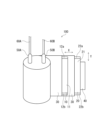
- FIG. It is a perspective view which shows a winding body typically.
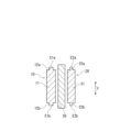
- FIG. 3 is a cross-sectional view schematically showing anode foil, cathode foil, and separators that constitute a wound body.
- FIG. 4 is a cross-sectional view schematically showing an electrolytic capacitor according to another embodiment of the present disclosure; It is a top view which shows a laminated body typically.
- FIG. 8 is a cross-sectional view taken along line VIII-VIII of FIG. 7;
- FIG. 1 is a front view showing a metal base sheet prepared in a first step of a method for manufacturing an electrolytic capacitor according to an embodiment of the present disclosure;
- FIG. 4 is a front view showing a metal base sheet having a conductive polymer layer formed on the surface of the first region by a coating process; [ Fig. 4]
- Fig. 4 is a front view showing a metal base sheet having a cut region compressed by a second step of a method for manufacturing an electrolytic capacitor according to an embodiment of the present disclosure.
- An electrolytic capacitor electrode foil includes a metal foil having a first region and a second region other than the first region.
- the second area is an area linearly extending along the edge of the metal foil and is a narrow strip-like area.
- the thickness of the second region is smaller than the thickness of the first region, and a step is provided between the first region and the second region on both surfaces of the metal foil.
- the first region may be strip-shaped.
- Electrode foil (metal foil) is obtained by cutting a metal base sheet into a predetermined size. At this time, burrs are generated at the edges of the electrode foil where the electrode foil is cut.
- the edge of the electrode foil and a member adjacent to the electrode foil (a member that may cause a short circuit due to contact with the electrode foil) when the capacitor element is formed. A large distance can be secured between As a result, even if burrs are present at the edges of the electrode foil, the insulation between the electrode foil and the member can be ensured. As a result, it is possible to suppress an increase in leakage current and the occurrence of short circuits caused by burrs, thereby improving the reliability of the electrolytic capacitor.
- the electrode foil according to the present disclosure may be used for at least one of the anode foil and the cathode foil.
- a large distance can be secured between the edges of the anode foil and the cathode foil, damage to the separator due to burrs can be suppressed, and insulation between the anode foil and the cathode foil can be secured.
- a distance greater than the thickness of the separator can be secured between the edges of the anode foil and the cathode foil, suppressing an increase in leakage current and the occurrence of short circuits even when winding misalignment or winding tightening occurs. can.
- tight winding is a phenomenon in which the separator is compressed due to tensile stress generated during winding, and the distance between the two electrode foils becomes narrower.
- the width of the separator is made larger than the width of the electrode foil in order to prevent contact between the two electrode foils due to winding misalignment. It is also possible to ensure a wider width of , which is advantageous in terms of increasing the capacity.
- the ratio of the area S2 of the second region to the area S1 of the first region when the electrode foil is viewed from the normal direction of the main surface: S2/S1 is, for example, 0.01 or more (or 0.05 or more), or 3 .0 or less, 0.01 or more (or 0.05 or more), or less than 1.0, 0.01 or more (or 0.05 or more), 0.75 or less (or 0 .5 or less).
- the main surface of the electrode foil is the "surface of the first region".
- the width of the second region is, for example, 0.1 mm or more and 10 mm or less (or 7 mm or less).
- the second region is formed by pressing a metal foil and T2/T1 (to be described later) is small (the degree of compression is large), impregnability of the conductive polymer in the second region tends to decrease, which affects the performance of the electrolytic capacitor.
- the area S2 of the second region (the width of the second region) is small.
- the second region is formed, for example, by pressing the edge of the metal foil in the thickness direction of the metal foil. Pressing is performed, for example, by roll-pressing the edges of the metal foil. In this case, the portion that is not pressed becomes the first region.
- T2/T1 which will be described later, can be controlled by the press pressure.
- the ratio of the thickness T2 of the second region to the thickness T1 of the first region: T2/T1 is preferably 0.60 or more and 0.95 or less, more preferably 0.70 or more and 0.90 or less.
- T2/T1 is in the range of 0.60 to 0.95.
- the edge portion of the metal foil includes a first edge portion extending in the longitudinal direction and a second edge portion opposite to the first edge portion.
- the second region is preferably at least one of a second A region linearly extending along the first edge and a second B region linearly extending along the second edge.
- the strip-shaped electrode foil is formed by slitting, and burrs may exist on the first edge and the second edge. Therefore, by using at least one (preferably both) of the 2A region and the 2B region as the second region, it is possible to efficiently suppress the short-circuit failure of the electrolytic capacitor.
- the width and thickness dimensions of the second A region and the second B region may be the same or different.
- the metal foil includes, for example, valve action metals such as aluminum, tantalum, niobium, and titanium.
- the metal foil may contain the valve action metal as an alloy or compound containing the valve action metal.
- the metal foil may be plain foil.
- the metal foil may be a foil having a roughened surface (etching foil), and may have a porous portion on the surfaces of the first region and the second region.
- the metal foil having a roughened surface has a porous portion and a core portion that is continuous with the porous portion, and may be an integral product of the porous portion and the core portion.
- the porous portion is formed by subjecting the surface of the metal foil to etching treatment, and the unetched portion of the metal foil remains as the core portion.
- the thickness of the porous portion is, for example, 1/10 or more and 4/10 or less of the total thickness of the metal foil.
- the porous portion has numerous pits (or pores) surrounded by metal portions.
- the mode pore diameter of the porous portion is, for example, 0.10 ⁇ m or more and 1.0 ⁇ m or less.
- the term "modal pore diameter" as used herein means the most frequent pore diameter (mode diameter) in the volume-based pore diameter distribution measured with a mercury porosimeter.
- the porous portion in the second region preferably has a smaller mode pore size than the porous portion in the first region.
- the second region is less impregnable with the conductive polymer than the first region, which is advantageous in terms of suppressing the occurrence of short circuits due to burrs at the edges of the metal foil.
- the electrode foil having the second region with low impregnability of the conductive polymer is used for at least one of the anode foil and the cathode foil in the wound body, the anode foil and the It is possible to suppress the occurrence of short circuits between the edges of the cathode foil via the conductive polymer.
- the ratio of the mode pore diameter P2 of the porous portion of the second region to the mode pore diameter P1 of the porous portion of the first region: P2/P1 is, for example, 0.3 or more and 0.8 or less (or 0.4 or more and 0.7 or less).
- the most frequent pore diameters P1 and P2 can be obtained by dividing the electrode foil into the first region and the second region and measuring each of them with a mercury porosimeter.
- the porous portion in the second region may have a smaller pit circumference than the porous portion in the first region.
- the “pit circumference length” is the total length of the outline of the pit inner walls included per unit area of the cross section in the thickness direction of the electrode foil (porous portion).
- the ratio of the pit circumference length L2 of the porous portion of the second region to the pit circumference length L1 of the porous portion of the first region: L2/L1 is, for example, 0.70 or more and 0.97 or less (or 0.75 or more and 0.98 or less).
- the above pit circumference length is obtained by the following method.
- a cross-sectional image of the electrode foil (porous portion) in the thickness direction is obtained using a scanning electron microscope (SEM) or a transmission electron microscope (TEM).
- SEM scanning electron microscope
- TEM transmission electron microscope
- Using the cross-sectional image of the porous portion of the first region five regions (area S: 50 ⁇ m 2 to 100 ⁇ m 2 ) within a range from the outer surface of the porous portion to a depth of 1/3 of the thickness of the porous portion.
- the total length L of the contour of the pit inner wall in each region is obtained, and the value (L/S) obtained by dividing the length L by the area S of the region is the pit circumference length of the porous portion of the first region ( ⁇ m/ ⁇ m 2 ).
- An average value of the pit perimeter lengths of the five regions is obtained.
- the pit circumference length of the porous portion in the second region is also obtained in the same manner.
- the porous portion of the second region may have a smaller thickness than the porous portion of the first region.
- the thickness of the porous portion of the second region is set to be greater than the thickness of the porous portion of the first region. can be made smaller.
- the ratio of the thickness TP2 of the porous portion of the second region to the thickness TP1 of the porous portion of the first region: TP2/TP1 is, for example, 0.60 or more and 0.95 or less (or 0.70 or more and 0 .90 or less).
- the thickness TP1 (or thickness TP2) of the porous portion of the first region (or the second region) is determined by any 10 points in the cross section in the thickness direction of the electrode foil (porous portion) of the first region (or the second region). It is obtained by measuring the thickness of and calculating the average value of them.
- the electrode foil may comprise a metal foil having porous portions on the surfaces of the first region and the second region, and a dielectric layer covering the surfaces of the porous portions.
- first electrode foil can be used as an anode foil (or anode body).
- the dielectric layer is formed, for example, by subjecting an etched foil to chemical conversion treatment (anodization).
- the dielectric layer includes an oxide of a valve metal (eg, an oxide of aluminum).
- the dielectric layer is formed along the uneven surface of the porous portion and is formed so as to cover the inner wall surfaces of the pits (or pores) of the porous portion.
- the thickness of the dielectric layer is, for example, 5 nm or more and 300 nm or less.
- the porous portion in the second region preferably has a smaller mode pore size than the first region, and may have a smaller thickness.
- the second region is less impregnable with the conductive polymer than the first region, which is advantageous in terms of suppressing the occurrence of short circuits due to burrs at the edges of the metal foil.
- impregnability of the conductive polymer is low in the second region, and contact between the defective portion of the dielectric layer and the conductive polymer is suppressed, and an increase in leakage current due to the contact is suppressed.
- the dielectric layer thinly covers the surfaces of the porous portions of the first and second regions. Therefore, in the first electrode foil having a dielectric layer on the surface, the ratio of the mode pore diameter PD2 of the porous portion in the second region to the mode pore diameter PD1 of the porous portion in the first region: PD2/PD1 is , is almost equivalent to the above P2/P1.
- the first electrode foil is formed, for example, by forming a porous portion on the surface of a metal foil, forming a dielectric layer covering the surface of the porous portion, and then pressing the metal foil along the edge to form the second electrode foil. Created by forming a region.
- the mode pore size is smaller in the porous portion of the second region than in the porous portion of the first region, and the thickness of the porous portion can also be reduced.
- the electrode foil may comprise a metal foil (plain foil or etched foil) and a coating layer covering the surfaces of the first and second regions of the metal foil.
- the coating layer may include at least one selected from the group consisting of metal oxide layers, metal nitride layers, metal carbide layers, and conductive layers.
- such electrode foil is also referred to as "second electrode foil”.
- the second electrode foil can be used as a cathode foil.
- the coating layer is formed for the purpose of enhancing corrosion resistance, electrical conductivity, and the like. Examples of metals contained in the coating layer include titanium, nickel, tantalum, and niobium.
- the metal contained in the coating layer may be the same as or different from the metal contained in the metal foil.
- the thickness of the coating layer is, for example, 10 nm or more and 5000 nm or less.
- the conductive layer may be a metal layer and/or a carbon layer. Also, carbon may be dispersed in the metal oxide layer, the metal nitride layer, or the conductive layer.
- the covering layer may consist, for example, of a metal oxide layer, a metal nitride layer and/or a metal layer and a carbon layer.
- the second electrode foil is produced, for example, by forming a coating layer on the surface of a metal foil (plain foil or etching foil) and then pressing along the edges of the metal foil to form the second region. be.
- FIG. 1 is a front view schematically showing an electrode foil for an electrolytic capacitor according to one embodiment of the present disclosure.
- FIG. 2 is a cross-sectional view schematically showing an electrode foil for electrolytic capacitors according to an embodiment of the present disclosure.
- the X direction and Y direction indicate the length direction and width direction of the strip-shaped electrode foil, respectively.
- the strip-shaped electrode foil 3 has a first edge E1 and a second edge E2 opposite to the first edge E1.
- the first edge E1 and the second edge E2 are edges extending in the X direction.
- the electrode foil 3 includes a first region 1, a second A region 2a linearly extending along the first edge E1, and a second B region 2b linearly extending along the second edge E2. have.
- the first region 1 has a thickness T1.
- the second A region 2a has a thickness T2.
- the second B region 2b also has substantially the same thickness T2 as the second A region 2a. Thickness T2 of second A region 2a and second B region 2b is smaller than thickness T1 of first region 1 .
- steps are provided between the first region 1 and the second A region 2a and the second B region 2b.
- the electrode foil 3 may be the first electrode foil or the second electrode foil.
- the ratio of the Y-direction length LW2 of the second A region 2a (second B region 2b) to the Y-direction length LW1 of the first region 1: LW2/LW1 is, for example, 0.01 or more (or 0.05 or more). , 3.0 or less, 0.01 or more (or 0.05 or more), or less than 1.0.
- the Y-direction length LW2 of the second A region 2a (the second B region 2b) is, for example, 0.1 mm or more and 10 mm or less (or 7 mm or less).
- the second A region 2a and the second B region 2b have the same thickness and width dimensions, but may have different thickness and/or width dimensions.
- An electrolytic capacitor according to an embodiment of the present disclosure includes a wound capacitor element.
- the capacitor element includes a wound body formed by winding a strip-shaped anode foil, a strip-shaped cathode foil facing the anode foil, and a separator arranged between the anode foil and the cathode foil.
- At least one of the anode foil and the cathode foil includes strip-shaped metal foil having a first region and a second region other than the first region.
- the metal foil has a first edge extending along its length and a second edge opposite to the first edge, and the second region is linear along the first edge. and at least one of a second A region extending linearly along the second edge.
- the thickness of the second region is smaller than the thickness of the first region, and a step is provided between the first region and the second region on both surfaces of the metal foil.
- a wound capacitor element may further include an electrolyte adhering to the wound body.
- An electrolyte is distributed over the dielectric layer and interposed between the anode and cathode foils.
- a wound capacitor element may include a conductive polymer (solid electrolyte) covering a dielectric layer.
- a conductive polymer solid electrolyte covering a dielectric layer.
- the second region is formed by pressing a metal foil, and T2/T1 at that time is relatively large (for example, T2/T1 is greater than 0.70), the conductive polymer is formed in the second region by pressing.
- the influence on the impregnability is kept small, and even if the area S2 of the second region is made relatively large (for example, larger than that of the first region), the performance of the electrolytic capacitor such as capacity is hardly affected.
- T2/T1 is small (for example, T2/T1 is 0.70 or less)
- the impregnation of the conductive polymer in the second region by pressing is greatly affected.
- the ratio of the area S2 of the second region to the area S1 of the first region: S2/S1 is more preferably 0.75 or less (or 0.5 or less), for example. In this case, the influence on the performance of the electrolytic capacitor can be kept small.
- the wound body may be impregnated with a treatment liquid containing a conductive polymer (solution or dispersion of a conductive polymer).
- a treatment liquid containing a conductive polymer may be applied to the surfaces of the electrode foils (anode foil and/or cathode foil) prior to formation.
- the treatment liquid containing the conductive polymer may be applied only to the first region.
- a dispersion containing conductive polymer particles having a diameter larger than the pit diameter of the porous portion of the second region is used as the treatment liquid, and the conductive polymer adheres to the second region (porous portion). You can reduce the amount.
- the anode foil includes a metal foil containing a valve metal and having a porous portion and a core portion continuous with the porous portion, and a dielectric layer covering the surface of the porous portion.
- the thickness of the anode foil is, for example, 60 ⁇ m or more and 200 ⁇ m or less.
- the anode foil is a first electrode foil having a first region and a second region, and the porous portion of the second region preferably has a smaller mode pore diameter than the porous portion of the first region.
- the coverage of the conductive polymer on the inner walls of the pits of the porous portion can be made smaller in the second region than in the first region.
- the ratio of the coverage C2 by the conductive polymer of the porous portion of the second region to the coverage C1 of the conductive polymer of the porous portion of the first region: C2/C1 is, for example, 0.10 or more, 0 0.95 or less (or 0.20 or more and 0.90 or less).
- the coverage of the porous portion with the conductive polymer is obtained by the following method.
- a cross-sectional image in the thickness direction of the electrode foil (porous portion) is obtained using SEM or TEM.
- five regions (area S: 50 ⁇ m 2 to 100 ⁇ m 2 ) within a range from the outer surface of the porous portion to a depth of 1/3 of the thickness of the porous portion.
- the total length L0 of the contours of the pit inner walls in each region and the length L1 of the contours of the portions of the pit inner walls covered with the conductive polymer are obtained, and the ratio (percentage) of L1 to L0 is obtained as the coverage. Calculate the average value of the coverage of the five regions.
- the second area is obtained in the same manner.
- cathode foil A metal foil containing a valve action metal can be used for the cathode foil.
- a plain foil is used as the metal foil, but an etched foil may be used as necessary.
- the cathode foil is preferably the electrode foil described above, and may be the second electrode foil.
- the thickness of the cathode foil is, for example, 20 ⁇ m or more and 60 ⁇ m or less.
- the separator is not particularly limited, and for example, a nonwoven fabric containing fibers of cellulose, polyethylene terephthalate, vinylon, polyamide (eg, aromatic polyamide such as aliphatic polyamide and aramid) may be used.
- a nonwoven fabric containing fibers of cellulose, polyethylene terephthalate, vinylon, polyamide eg, aromatic polyamide such as aliphatic polyamide and aramid
- polyamide eg, aromatic polyamide such as aliphatic polyamide and aramid
- the electrolyte covers at least part of the anode foil (dielectric layer) and is interposed between the anode foil (dielectric layer) and the cathode foil.
- the electrolyte includes at least one of a solid electrolyte and an electrolytic solution.
- a solid electrolyte and an electrolytic solution or a non-aqueous solvent may be used in combination.
- the electrolytic solution and the non-aqueous solvent are collectively referred to as "liquid component".
- the solid electrolyte contains a conductive polymer and may contain a dopant together with the conductive polymer.
- conductive polymers include ⁇ -conjugated polymers.
- conductive polymers include polypyrrole, polythiophene, polyaniline, derivatives thereof, and the like. Derivatives of polythiophene include poly(3,4-ethylenedioxythiophene) and the like.
- Dopants include polystyrene sulfonic acid and the like. The conductive polymer and dopant may be used singly or in combination of two or more.
- the electrolyte contains a non-aqueous solvent and a solute (eg, organic salt) dissolved therein.
- the non-aqueous solvent may be an organic solvent or an ionic liquid.
- a solvent with a high boiling point is preferable as the non-aqueous solvent.
- examples include polyol compounds such as ethylene glycol, sulfone compounds such as sulfolane, lactone compounds such as ⁇ -butyrolactone, ester compounds such as methyl acetate, carbonate compounds such as propylene carbonate, ether compounds such as 1,4-dioxane, and methyl ethyl ketone.
- a ketone compound or the like can be used.
- An organic salt is a salt in which at least one of the anion and cation contains an organic substance.
- organic salts include trimethylamine maleate, triethylamine borodisalicylate, ethyldimethylamine phthalate, mono-1,2,3,4-tetramethylimidazolinium phthalate, mono-1,3-dimethyl-2-phthalate, Ethylimidazolinium and the like may also be used.
- the liquid component may contain an acid component (anion) and a base component (cation).
- a salt may be formed by the acid component and the base component.
- acid components include organic carboxylic acids and inorganic acids.
- inorganic acids include phosphoric acid, boric acid, and sulfuric acid.
- base component include primary to tertiary amine compounds.
- FIG. 3 is a cross-sectional view schematically showing an electrolytic capacitor according to one embodiment of the present disclosure.
- FIG. 4 is a perspective view schematically showing the configuration of the wound body of FIG. 3.
- FIG. 4 the X direction indicates the length direction of strip-shaped anode foil 10 and cathode foil 20
- the Y direction indicates the width direction of anode foil 10 and cathode foil 20 .
- FIG. 5 is a cross-sectional view schematically showing the configuration of anode foil 10, cathode foil 20, and separator 30. As shown in FIG.
- the electrolytic capacitor 200 includes a wound body 100.
- the wound body 100 is constructed by winding an anode foil 10 and a cathode foil 20 with a separator 30 interposed therebetween.
- the wound body 100 has a height Lc.
- the direction of height Lc can also be said to be the Y direction of anode foil 10 and cathode foil 20 .
- the strip-shaped anode foil 10 has a first edge E1a extending in its length direction (X direction) and a second edge E1b opposite to the first edge E1a.
- Anode foil 10 includes first region 11, second A region 12a linearly extending along first edge E1a, and second B region 12b linearly extending along second edge E1b. have.
- the thicknesses of second A region 12a and second B region 12b are each smaller than the thickness of first region 11, and on both surfaces of anode foil 10, between first region 11 and second A region 12a A step is provided, and a step is provided between the first region 11 and the second B region 12b.
- the strip-shaped cathode foil 20 has a first edge E2a extending in its length direction (X direction) and a second edge E2b opposite to the first edge E2a.
- the cathode foil 20 includes a first region 21, a second A region 22a linearly extending along the first edge E2a, and a second B region 22b linearly extending along the second edge E2b. have.
- the thicknesses of the second A region 22a and the second B region 22b are each smaller than the thickness of the first region 21, and on both surfaces of the cathode foil 20, between the first region 21 and the second A region 22a A step is provided, and a step is provided between the first region 21 and the second B region 22b.
- the first edge E1a and the second edge E1b of the anode foil 10 and the second A region 22a and the second B region 22b of the cathode foil 20 By the second A region 12a and the second B region 12b of the anode foil 10 and the second A region 22a and the second B region 22b of the cathode foil 20, the first edge E1a and the second edge E1b of the anode foil 10, and , a large distance between the anode foil 10 and the cathode foil 20 is ensured at the first end edge E2a and the second end edge E2b of the cathode foil 20 .
- the burrs present at the edges of the anode foil and the cathode foil are prevented from breaking through the separators, and the occurrence of short circuits caused by the burrs penetrating the separators is suppressed.
- 2nd A region 12a, 2nd B region 12b, 2nd A region 22a, and 2nd B region 22b provide edge portions E1a and E1b of anode foil 10 and edge portion E2a of cathode foil 20 when wound body 100 is formed.
- E2b a distance equal to or greater than the thickness of the separator 30 can be secured. As a result, it is possible to suppress an increase in leakage current and the occurrence of short-circuit defects even when winding misalignment or winding tightening occurs.
- Lead tabs 50A and 50B are connected to the anode foil 10 and the cathode foil 20, respectively, and the wound body 100 is formed by winding the lead tabs 50A and 50B.
- Lead wires 60A and 60B are connected to the other ends of lead tabs 50A and 50B, respectively.
- a winding stop tape 40 is arranged on the outer surface of the cathode foil 20 located in the outermost layer of the wound body 100 , and the ends of the cathode foil 20 are fixed by the winding stop tape 40 .
- the anode foil 10 is prepared by cutting from a large-sized foil, the rolled body 100 may be further subjected to a chemical conversion treatment in order to provide a dielectric layer on the cut surface.
- the electrolyte adheres to the wound body 100, and is interposed between the anode foil 10 (dielectric layer) and the cathode foil.
- the anode foil 10 dielectric layer
- the cathode foil For example, by impregnating wound body 100 with a treatment liquid containing a conductive polymer, the surface of anode foil 10 (dielectric layer) can be covered with the conductive polymer. Impregnation may be performed under reduced pressure, for example in an atmosphere of 10 kPa to 100 kPa.
- the wound body 100 is housed in the bottomed case 211 so that the lead wires 60A and 60B are located on the opening side of the bottomed case 211.
- metals such as aluminum, stainless steel, copper, iron, and brass, or alloys thereof can be used.
- a sealing member 212 is placed in the opening of the bottomed case 211 in which the wound body 100 is accommodated, and the opening end of the bottomed case 211 is crimped to the sealing member 212 for curling, and the seat plate 213 is attached to the curled portion. By arranging them, the wound body 100 is sealed in the bottomed case 211 .
- the sealing member 212 is formed so that the lead wires 60A and 60B pass therethrough.
- the sealing member 212 may be an insulating material, preferably an elastic material. Among them, highly heat-resistant silicone rubber, fluorine rubber, ethylene propylene rubber, hypalon rubber, butyl rubber, isoprene rubber and the like are preferable.
- An electrolytic capacitor includes a laminate obtained by laminating a plurality of laminated capacitor elements.
- the capacitor element includes a metal foil having a cathode forming portion and an anode lead-out portion extending from one edge portion of the cathode forming portion and having a porous portion on the surface thereof, a dielectric layer covering the cathode forming portion, and a dielectric layer. an overlying cathode portion.
- the cathode forming portion has a first region and a second region other than the first region, and the second region is a line extending along an edge portion other than the one edge portion of the cathode forming portion.
- the second region has a smaller thickness than the first region, and a step is provided between the first region and the second region on both surfaces of the metal foil.
- the cathode section includes, for example, a solid electrolyte layer covering the dielectric layer, and a cathode extraction layer covering the solid electrolyte layer.
- the cathode portions (cathode extraction layers) of adjacent capacitor elements may be in close contact with each other via an adhesive layer formed of a conductive adhesive.
- the laminated portion may be formed by overlapping the ends of the anode lead-out portions of the plurality of capacitor elements.
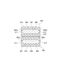
- FIG. 6 is a cross-sectional view schematically showing an electrolytic capacitor according to another embodiment of the present disclosure.
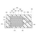
- FIG. 7 is a top view schematically showing a laminate.
- capacitor element 402 first region 461 and second A region 462a to second C region 462c of anode body 460 covered with cathode portion 408 are indicated by dashed lines.
- 8 is a cross-sectional view taken along line VIII-VIII of FIG. 7.
- the electrolytic capacitor 400 includes a laminate 401 , an anode lead terminal 404 and a cathode lead terminal 405 electrically connected to the laminate 401 , and a resin-made exterior body 403 that seals the laminate 401 . A part of the anode lead terminal 404 and the cathode lead terminal 405 is covered with the exterior body 403 .
- the exterior body 403 has a substantially rectangular parallelepiped outer shape, and the electrolytic capacitor 400 also has a substantially rectangular parallelepiped outer shape.
- the laminate 401 is configured by laminating a plurality of capacitor elements 402 .
- Capacitor elements 402 (cathode portions 408) adjacent to each other are electrically connected via an adhesive layer 415 formed of a conductive adhesive.
- an adhesive layer 415 formed of a conductive adhesive.
- two capacitor elements are stacked, but the number of capacitor elements forming the laminate is not limited to this.
- Capacitor element 402 includes metal foil 406 having cathode forming portion 406a and anode lead-out portion 406b extending from one edge (fourth edge E14) of cathode forming portion 406a, and dielectric layer 407 covering cathode forming portion 406a. and a cathode portion 408 covering the dielectric layer 407 .
- Metal foil 406 (cathode forming portion 406 a and anode leading portion 406 b ) has a porous portion on its surface, and dielectric layer 407 is formed to cover the surface of the porous portion of cathode forming portion 406 .
- Cathode formation portion 406 a and dielectric layer 407 constitute anode body 460 .
- the anode body 460 (cathode forming portion 406a) has a first end edge portion E11 to a third end edge portion E13.
- the edges E11-E13 can be formed by cutting.
- Anode body 460 includes first region 461, second A region 462a linearly extending along first edge E11, second B region 462b linearly extending along second edge E12, and second and a second C region 462c linearly extending along the third edge E13.
- Each of the second A region 462a to the second C region 462c has a smaller thickness than the first region 461.
- Steps are provided between the first region 461 and the second A region 462a to the second C region 462c on both surfaces of the anode body 460 (cathode forming portion 406a).
- a second region is formed by the second A region 462a to the second C region 462c.
- the cathode portion solid electrolyte layer, cathode extraction layer
- the cathode portion solid electrolyte layer, cathode extraction layer
- a conductive adhesive is used to bond adjacent capacitor elements together. The bonding is performed by applying a constant pressure to the laminate to bring the capacitor elements into close contact with each other. Therefore, when forming the laminate, pressure may be applied to the capacitor element having burrs.
- pressure may be applied to the capacitor element having burrs when forming an exterior body covering the laminate by injection molding of a resin material, or when heat or vibration is transmitted to the electrolytic capacitor due to reflow processing or the like.
- the burrs covered with the cathode portion press the adjacent capacitor element (dielectric layer), thereby causing defects in the dielectric layer and increasing leakage current. be.
- the burr covered with the cathode portion may break through the dielectric layer of the adjacent capacitor element, causing contact between the cathode portion and the metal substrate of the anode body, resulting in short-circuit failure.
- the edge portions (first edge portions E11 A large distance is ensured between the ⁇ third edge portions E13).
- pressure on the adjacent capacitor element (dielectric layer) due to the burr is suppressed, resulting in an increase in leakage current and occurrence of a short circuit. can be suppressed.
- An insulating separation layer 413 is formed in a portion adjacent to the cathode portion 408 in the anode lead-out portion 406 b to restrict contact between the cathode portion 408 and the anode body 460 .
- the end portions of the plurality of anode lead-out portions 406b are stacked and integrated into one to form a stacked portion.
- the stacked portion of the plurality of anode lead-out portions 406b and the anode lead terminal 404 are electrically connected by welding.
- the cathode portion 408 at the end of the laminate 401 and the cathode lead terminal 405 are electrically connected via an adhesive layer 414 formed of a conductive adhesive.
- the cathode section 408 includes a solid electrolyte layer 409 covering the dielectric layer 407 and a cathode extraction layer 410 covering the solid electrolyte layer 409 .
- Cathode extraction layer 410 has carbon layer 411 and silver paste layer 412 .
- the carbon layer 411 contains, for example, carbon particles and silver.
- Silver paste layer 412 includes, for example, silver particles and a binder.
- the binder is not particularly limited, a cured product of a curable resin is preferable.
- curable resins include thermosetting resins such as epoxy resins.
- the solid electrolyte layer 409 contains a conductive polymer, and may contain a dopant or the like as necessary.
- conductive polymers examples include polypyrrole, polythiophene, polyaniline, and derivatives thereof.
- Solid electrolyte layer 409 is formed by, for example, coating or impregnating the surface of anode body 460 having a first region and a second region with a treatment liquid containing a conductive polymer (solution or dispersion of a conductive polymer). can be formed.
- a treatment liquid containing a conductive polymer may be applied only to the first region 461 to form a solid electrolyte layer, thereby forming a cathode portion.
- the exterior body 403 preferably contains a cured product of a curable resin composition, and may contain a thermoplastic resin or a composition containing it.
- curable resins include thermosetting resins such as epoxy resins.
- a manufacturing method of an electrolytic capacitor includes a first step, a second step (pressing step), and a third step (cutting step).
- a metal substrate sheet having a plurality of first regions and a plurality of cutting regions alternately arranged in stripes is prepared.
- the cut area is compressed in the thickness direction of the metal base sheet.
- the widthwise central portion of the cut area is cut along the length direction of the cut area to obtain a plurality of electrode foils.
- the width of the cutting area is preferably smaller than the width of the first area.
- the metal base sheet may be a plain foil or an etched foil.
- the metal substrate sheet may be a sheet having a dielectric layer on its surface, or a sheet having a coating layer on its surface.
- the metal base sheet prepared in the first step contains a valve action metal.
- a metal base sheet having a dielectric layer on its surface may be prepared.
- the first step may include a step of roughening the surface of the metal substrate sheet to form a porous portion.
- the first step may include forming a dielectric layer covering the surface of the porous portion.
- the electrode foil obtained in the third step can be used as the anode foil.
- the cut area of the metal base sheet is roll-pressed.
- a strip-shaped metal substrate sheet with a width of 10 mm or more and 500 mm or less is slit into widths of 2 mm or more and 100 mm or less to obtain a plurality of strip-shaped electrode foils.
- a device equipped with rolls for conveying the metal base sheet, rolling rolls and slitting blades provided on the conveying path may be used.
- the mill rolls and blades are arranged respectively upstream and downstream of the conveying path.
- a plurality of rolling rolls and blades are arranged at regular intervals at positions corresponding to a plurality of cutting areas.
- the pressing and slitting of a plurality of cutting regions can be performed at once by a plurality of rolling rolls and blades, the positioning of the pressing and slitting is easy, and the second and third steps can be performed efficiently. can be done.
- the manufacturing method may include a step of applying a treatment liquid containing a conductive polymer to the first region of the metal base sheet (application step).
- a step of applying a treatment liquid containing a conductive polymer to a first region of a metal base sheet having a dielectric layer on its surface is performed to form a conductive polymer layer (solid electrolyte layer) covering the surface of the dielectric layer.
- the coating step is preferably performed after the second step and before the third step, and may be performed before the second step.
- a coating method such as gravure coating is used.
- the second region may not be coated with the treatment liquid containing the conductive polymer.
- FIG. 9 is a front view showing a metal substrate sheet prepared in the first step.
- FIG. 10 is a front view showing a metal substrate sheet having a conductive polymer layer formed on the surface of the first region.
- FIG. 11 is a front view showing a metal base sheet with a compressed cut area. 10 and 11, hatched areas indicate areas where the conductive polymer layer is formed.
- a sheet 300 (metal base sheet) shown in FIG. 9 has a plurality of first regions 301 and a plurality of cutting regions 302 alternately arranged in stripes.
- cut areas 302 of the same width are provided at regular intervals.
- the width of the cutting area 302 is narrower than the width of the first area 301 .
- the compressed area 312 shown in FIG. 11 is formed.
- the second region A plurality of strip-shaped electrode foils having
- a strip-shaped anode foil and a strip-shaped cathode foil are wound in the length direction of the anode foil and the cathode foil with a separator interposed between the anode foil and the cathode foil.
- a step of obtaining a body may be included.
- At least one of the anode foil and the cathode foil may be an electrode foil obtained by the above manufacturing method (including the first to third steps and, if necessary, a coating step).
- the manufacturing method may include a step of impregnating the wound body with a treatment liquid containing a conductive polymer.
- a treatment liquid containing a conductive polymer When the coating step is not performed, it is desirable to perform the step of impregnating the wound body.
- a metal substrate sheet (thickness 100 ⁇ m) having a plurality of first regions (5.0 mm wide) and a plurality of cut regions (0.3 mm wide) alternately arranged in stripes was prepared (first step).
- Etched foil with a dielectric layer on the surface was used for the metal base sheet.
- the etched foil was obtained by etching an Al foil having a thickness of 100 ⁇ m to form a porous portion (thickness per side: 35 ⁇ m, mode pore diameter: 0.15 ⁇ m) on the surface of the Al foil.
- the dielectric layer was obtained by chemically converting the etched foil to form an aluminum oxide layer (thickness 70 nm).
- a plurality of belt-shaped anode foils were obtained by cutting the central portion of the cut region in the width direction along the length direction of the cut region (third step).
- the anode foil has a first region (thickness T1: 100 ⁇ m), a second A region linearly extending along the first edge, and a second B region linearly extending along the second edge. had.
- the thickness T2 of the 2nd A region and the 2nd B region was the value shown in Table 1.
- the width dimension of the first region (the length in the Y direction of the first region 1 in FIG. 1) was 5.0 mm.
- the width dimension of the 2A region and the 2B region (length in the Y direction of the 2A region 2a and the 2B region 2b in FIG. 1) was 0.15 mm.
- an etching foil having a chemical conversion film on its surface and cut into a predetermined size was used as the cathode foil.
- the etching foil was obtained by etching an Al foil having a thickness of 50 ⁇ m to form a porous portion (thickness per side: 15 ⁇ m, mode pore diameter: 0.12 ⁇ m) on the surface of the Al foil.
- the chemical conversion coating was obtained by subjecting the etched foil to chemical conversion treatment to form an aluminum oxide layer (thickness: 5 nm).
- An anode lead tab and a cathode lead tab to which lead wires were connected were connected to the prepared anode foil and cathode foil, respectively. Then, the anode foil and the cathode foil were wound with a separator sandwiched therebetween, and the outer surfaces were fixed with a winding stop tape. Thus, a wound body was produced.
- the anode foil was chemically treated again to form a dielectric layer on the end surface of the anode foil.
- the capacitor element After housing the capacitor element in the bottomed case, the capacitor element was impregnated with the electrolytic solution at room temperature under atmospheric pressure.
- the electrolytic solution a solution containing triethylamine phthalate dissolved in ethylene glycol as a main component was used.
- a sealing member and a seat plate were placed in the opening of the bottomed case to seal the capacitor element.
- an electrolytic capacitor was completed.
- an aging treatment was performed at 105° C. for 2 hours while applying a rated voltage.
- A1 to A6 in Table 1 indicate the electrolytic capacitors of Examples 1 to 6, respectively.
- Table 1 shows the evaluation results.
- the distance between the edge portions of the anode foil and the cathode foil was increased, and damage to the separator due to burrs present at the edge portions of the electrode foils was suppressed.
- the initial LC defect rate was small, and the leakage current after vibration was also small.
- burrs existing at the edges of the electrode foil increased the initial LC defect rate and increased the leakage current after vibration.
- an etching foil having a dielectric layer on its surface and cut into a predetermined size was used as the anode foil.
- the etched foil was obtained by etching an Al foil having a thickness of 100 ⁇ m to form a porous portion (thickness per side: 35 ⁇ m, mode pore diameter: 0.15 ⁇ m) on the surface of the Al foil.
- the dielectric layer was obtained by chemically converting the etched foil to form an aluminum oxide layer (thickness 70 nm).
- a metal substrate sheet having a plurality of first regions (50 ⁇ m thick, 5.0 mm wide) and a plurality of cut regions (50 ⁇ m thick, 0.3 mm wide) alternately arranged in stripes was prepared (first step).
- the metal base sheet An etched foil with a chemical conversion film on the surface was used as the metal base sheet.
- the etching foil was obtained by etching an Al foil having a thickness of 50 ⁇ m to form a porous portion (thickness per side: 15 ⁇ m, mode pore diameter: 0.12 ⁇ m) on the surface of the Al foil.
- the chemical conversion coating was obtained by subjecting the etched foil to chemical conversion treatment to form an aluminum oxide layer (thickness: 5 nm).
- a plurality of band-shaped cathode foils were obtained by cutting the center portion of the cut region in the width direction along the length direction of the cut region (third step).
- the cathode foil has a first region (thickness T1: 50 ⁇ m), a second A region linearly extending along the first edge, and a second B region linearly extending along the second edge. had.
- the thickness T2 of the 2nd A region and the 2nd B region was the value shown in Table 1.
- the width dimension of the first region (the length in the Y direction of the first region 1 in FIG. 1) was 5.0 mm.
- the width dimension of the 2A region and the 2B region (length in the Y direction of the 2A region 2a and the 2B region 2b in FIG. 1) was 0.15 mm.
- Electrolytic capacitors A7 to A12 were produced in the same manner as in Example 1, except that the anode foil prepared above and the cathode foil obtained above were used.
- Evaluation 1 and Evaluation 2 above were performed for electrolytic capacitors A7 to A12.
- Table 2 shows the evaluation results.
- Table 2 also shows the evaluation results of the electrolytic capacitor B1.
- the distance between the edges of the anode foil and the cathode foil was increased, and damage to the separator due to burrs present at the edges of the electrode foils was suppressed.
- the electrolytic capacitors A7 to A12 had a smaller initial LC defect rate and a smaller leakage current after vibration than the electrolytic capacitor B1.
- the electrode foil according to the present disclosure is suitable for use in electrolytic capacitors that require high reliability.
Landscapes
- Engineering & Computer Science (AREA)
- Power Engineering (AREA)
- Microelectronics & Electronic Packaging (AREA)
- Chemical & Material Sciences (AREA)
- Chemical Kinetics & Catalysis (AREA)
- Electrochemistry (AREA)
- Manufacturing & Machinery (AREA)
- Materials Engineering (AREA)
- Fixed Capacitors And Capacitor Manufacturing Machines (AREA)
Priority Applications (3)
| Application Number | Priority Date | Filing Date | Title |
|---|---|---|---|
| JP2023565020A JPWO2023100888A1 (https=) | 2021-11-30 | 2022-11-29 | |
| US18/712,152 US20250022664A1 (en) | 2021-11-30 | 2022-11-29 | Electrolytic capacitor-use electrode foil, electrolytic capacitor, and electrolytic capacitor manufacturing method |
| CN202280078588.5A CN118318283A (zh) | 2021-11-30 | 2022-11-29 | 电解电容器用电极箔、电解电容器以及电解电容器的制造方法 |
Applications Claiming Priority (2)
| Application Number | Priority Date | Filing Date | Title |
|---|---|---|---|
| JP2021194887 | 2021-11-30 | ||
| JP2021-194887 | 2021-11-30 |
Publications (1)
| Publication Number | Publication Date |
|---|---|
| WO2023100888A1 true WO2023100888A1 (ja) | 2023-06-08 |
Family
ID=86612205
Family Applications (1)
| Application Number | Title | Priority Date | Filing Date |
|---|---|---|---|
| PCT/JP2022/044008 Ceased WO2023100888A1 (ja) | 2021-11-30 | 2022-11-29 | 電解コンデンサ用電極箔、電解コンデンサ、および電解コンデンサの製造方法 |
Country Status (4)
| Country | Link |
|---|---|
| US (1) | US20250022664A1 (https=) |
| JP (1) | JPWO2023100888A1 (https=) |
| CN (1) | CN118318283A (https=) |
| WO (1) | WO2023100888A1 (https=) |
Citations (4)
| Publication number | Priority date | Publication date | Assignee | Title |
|---|---|---|---|---|
| JPH01251605A (ja) * | 1988-03-30 | 1989-10-06 | Marcon Electron Co Ltd | 固体電解コンデンサ |
| JP2008166315A (ja) * | 2006-12-26 | 2008-07-17 | Nippon Chemicon Corp | 固体電解コンデンサおよびその製造方法 |
| JP2014022707A (ja) * | 2012-07-12 | 2014-02-03 | Japan Capacitor Industrial Co Ltd | アルミニウム電解コンデンサ用陰極箔 |
| WO2015118901A1 (ja) * | 2014-02-07 | 2015-08-13 | 株式会社村田製作所 | コンデンサ |
-
2022
- 2022-11-29 CN CN202280078588.5A patent/CN118318283A/zh active Pending
- 2022-11-29 US US18/712,152 patent/US20250022664A1/en active Pending
- 2022-11-29 JP JP2023565020A patent/JPWO2023100888A1/ja active Pending
- 2022-11-29 WO PCT/JP2022/044008 patent/WO2023100888A1/ja not_active Ceased
Patent Citations (4)
| Publication number | Priority date | Publication date | Assignee | Title |
|---|---|---|---|---|
| JPH01251605A (ja) * | 1988-03-30 | 1989-10-06 | Marcon Electron Co Ltd | 固体電解コンデンサ |
| JP2008166315A (ja) * | 2006-12-26 | 2008-07-17 | Nippon Chemicon Corp | 固体電解コンデンサおよびその製造方法 |
| JP2014022707A (ja) * | 2012-07-12 | 2014-02-03 | Japan Capacitor Industrial Co Ltd | アルミニウム電解コンデンサ用陰極箔 |
| WO2015118901A1 (ja) * | 2014-02-07 | 2015-08-13 | 株式会社村田製作所 | コンデンサ |
Also Published As
| Publication number | Publication date |
|---|---|
| JPWO2023100888A1 (https=) | 2023-06-08 |
| CN118318283A (zh) | 2024-07-09 |
| US20250022664A1 (en) | 2025-01-16 |
Similar Documents
| Publication | Publication Date | Title |
|---|---|---|
| JP7390601B2 (ja) | 蓄電デバイス | |
| CN102903523B (zh) | 电解电容器和其制造方法 | |
| CN102646515B (zh) | 电解电容器及电解电容器的制造方法 | |
| US9287051B2 (en) | Electrolytic capacitor and method for manufacturing same | |
| KR101029451B1 (ko) | 전해 콘덴서와 그 제조 방법 | |
| US10755865B2 (en) | Electrolytic capacitor and method for manufacturing same | |
| CN109074960B (zh) | 电解电容器及其制造方法 | |
| US8218293B2 (en) | Winding-type electrolytic capacitor and method of manufacturing the same | |
| WO2016189779A1 (ja) | 電解コンデンサ | |
| US12542246B2 (en) | Electrode foil for electrolytic capacitor having improved reliability and capacity, electrolytic capacitor, and method for manufacturing electrode foil for electrolytic capacitor | |
| JP2010074083A (ja) | 電解コンデンサおよびその製造方法 | |
| WO2023100888A1 (ja) | 電解コンデンサ用電極箔、電解コンデンサ、および電解コンデンサの製造方法 | |
| WO2024162155A1 (ja) | 電解コンデンサ用電極箔、電解コンデンサ、および電解コンデンサ用電極箔の製造方法 | |
| JP7839980B2 (ja) | 電解コンデンサ用電極箔および電解コンデンサ | |
| JP2010074089A (ja) | 電解コンデンサおよびその製造方法 | |
| US20260106086A1 (en) | Electrode foil for electrolytic capacitor, electrolytic capacitor, and production method for electrode foil for electrolytic capacitor | |
| US20250062078A1 (en) | Electrolytic capacitor and production method for same | |
| WO2026094814A1 (ja) | 電解コンデンサ | |
| WO2024162156A1 (ja) | 電解コンデンサおよびその製造方法 | |
| WO2023182509A1 (ja) | 電解コンデンサ用セパレータの製造方法、電解コンデンサの製造方法、電解コンデンサ用セパレータ、および電解コンデンサ | |
| WO2023120708A1 (ja) | 電解コンデンサおよび電解コンデンサの製造方法 | |
| WO2026029005A1 (ja) | 電極箔、電解コンデンサ、および電極箔の製造方法 | |
| WO2024116845A1 (ja) | 電解コンデンサの製造方法、電解コンデンサ、第1処理液、および第2処理液 | |
| WO2022210513A1 (ja) | 電解コンデンサの製造方法 | |
| JPH0794366A (ja) | 電解コンデンサの製造方法 |
Legal Events
| Date | Code | Title | Description |
|---|---|---|---|
| 121 | Ep: the epo has been informed by wipo that ep was designated in this application |
Ref document number: 22901320 Country of ref document: EP Kind code of ref document: A1 |
|
| ENP | Entry into the national phase |
Ref document number: 2023565020 Country of ref document: JP Kind code of ref document: A |
|
| WWE | Wipo information: entry into national phase |
Ref document number: 18712152 Country of ref document: US |
|
| WWE | Wipo information: entry into national phase |
Ref document number: 202280078588.5 Country of ref document: CN |
|
| NENP | Non-entry into the national phase |
Ref country code: DE |
|
| 122 | Ep: pct application non-entry in european phase |
Ref document number: 22901320 Country of ref document: EP Kind code of ref document: A1 |