WO2023100888A1 - Electrolytic capacitor-use electrode foil, electrolytic capacitor, and electrolytic capacitor manufacturing method - Google Patents
Electrolytic capacitor-use electrode foil, electrolytic capacitor, and electrolytic capacitor manufacturing method Download PDFInfo
- Publication number
- WO2023100888A1 WO2023100888A1 PCT/JP2022/044008 JP2022044008W WO2023100888A1 WO 2023100888 A1 WO2023100888 A1 WO 2023100888A1 JP 2022044008 W JP2022044008 W JP 2022044008W WO 2023100888 A1 WO2023100888 A1 WO 2023100888A1
- Authority
- WO
- WIPO (PCT)
- Prior art keywords
- region
- foil
- electrolytic capacitor
- cathode
- edge
- Prior art date
Links
- 239000011888 foil Substances 0.000 title claims abstract description 319
- 239000003990 capacitor Substances 0.000 title claims description 120
- 238000004519 manufacturing process Methods 0.000 title claims description 21
- 229910052751 metal Inorganic materials 0.000 claims abstract description 118
- 239000002184 metal Substances 0.000 claims abstract description 118
- 239000010410 layer Substances 0.000 claims description 111
- 229920001940 conductive polymer Polymers 0.000 claims description 55
- 238000005520 cutting process Methods 0.000 claims description 21
- 239000011148 porous material Substances 0.000 claims description 21
- 238000004804 winding Methods 0.000 claims description 20
- 239000007788 liquid Substances 0.000 claims description 16
- 239000007784 solid electrolyte Substances 0.000 claims description 16
- 239000011247 coating layer Substances 0.000 claims description 12
- 238000000034 method Methods 0.000 claims description 12
- 238000000605 extraction Methods 0.000 claims description 7
- 229910044991 metal oxide Inorganic materials 0.000 claims description 4
- 150000004706 metal oxides Chemical class 0.000 claims description 4
- 150000004767 nitrides Chemical class 0.000 claims description 4
- 238000007788 roughening Methods 0.000 claims description 2
- 238000005868 electrolysis reaction Methods 0.000 claims 1
- 238000003825 pressing Methods 0.000 description 18
- 238000005530 etching Methods 0.000 description 12
- -1 polyethylene terephthalate Polymers 0.000 description 11
- 238000011156 evaluation Methods 0.000 description 10
- 238000000576 coating method Methods 0.000 description 9
- 239000000126 substance Substances 0.000 description 9
- 239000000758 substrate Substances 0.000 description 9
- OKTJSMMVPCPJKN-UHFFFAOYSA-N Carbon Chemical compound [C] OKTJSMMVPCPJKN-UHFFFAOYSA-N 0.000 description 7
- 229910052799 carbon Inorganic materials 0.000 description 7
- 239000011248 coating agent Substances 0.000 description 7
- 230000007547 defect Effects 0.000 description 7
- 239000003792 electrolyte Substances 0.000 description 7
- 238000007789 sealing Methods 0.000 description 7
- LYCAIKOWRPUZTN-UHFFFAOYSA-N Ethylene glycol Chemical compound OCCO LYCAIKOWRPUZTN-UHFFFAOYSA-N 0.000 description 6
- 238000006243 chemical reaction Methods 0.000 description 6
- 239000006185 dispersion Substances 0.000 description 6
- 230000001965 increasing effect Effects 0.000 description 6
- 229920005989 resin Polymers 0.000 description 6
- 239000011347 resin Substances 0.000 description 6
- BQCADISMDOOEFD-UHFFFAOYSA-N Silver Chemical compound [Ag] BQCADISMDOOEFD-UHFFFAOYSA-N 0.000 description 5
- 239000003125 aqueous solvent Substances 0.000 description 5
- 230000015572 biosynthetic process Effects 0.000 description 5
- 239000008151 electrolyte solution Substances 0.000 description 5
- 239000000463 material Substances 0.000 description 5
- 150000003839 salts Chemical class 0.000 description 5
- 229910052709 silver Inorganic materials 0.000 description 5
- 239000004332 silver Substances 0.000 description 5
- 239000000853 adhesive Substances 0.000 description 4
- 230000001070 adhesive effect Effects 0.000 description 4
- 239000012790 adhesive layer Substances 0.000 description 4
- 239000002019 doping agent Substances 0.000 description 4
- TWNQGVIAIRXVLR-UHFFFAOYSA-N oxo(oxoalumanyloxy)alumane Chemical compound O=[Al]O[Al]=O TWNQGVIAIRXVLR-UHFFFAOYSA-N 0.000 description 4
- 238000002360 preparation method Methods 0.000 description 4
- 238000012360 testing method Methods 0.000 description 4
- ZWEHNKRNPOVVGH-UHFFFAOYSA-N 2-Butanone Chemical compound CCC(C)=O ZWEHNKRNPOVVGH-UHFFFAOYSA-N 0.000 description 3
- ZMANZCXQSJIPKH-UHFFFAOYSA-N Triethylamine Chemical compound CCN(CC)CC ZMANZCXQSJIPKH-UHFFFAOYSA-N 0.000 description 3
- 239000002253 acid Substances 0.000 description 3
- 229910052782 aluminium Inorganic materials 0.000 description 3
- XAGFODPZIPBFFR-UHFFFAOYSA-N aluminium Chemical compound [Al] XAGFODPZIPBFFR-UHFFFAOYSA-N 0.000 description 3
- 230000006378 damage Effects 0.000 description 3
- 230000002950 deficient Effects 0.000 description 3
- 238000010030 laminating Methods 0.000 description 3
- 150000002739 metals Chemical class 0.000 description 3
- 239000002245 particle Substances 0.000 description 3
- 229920000172 poly(styrenesulfonic acid) Polymers 0.000 description 3
- 229940005642 polystyrene sulfonic acid Drugs 0.000 description 3
- 229920000123 polythiophene Polymers 0.000 description 3
- 238000005096 rolling process Methods 0.000 description 3
- 239000000243 solution Substances 0.000 description 3
- YEJRWHAVMIAJKC-UHFFFAOYSA-N 4-Butyrolactone Chemical compound O=C1CCCO1 YEJRWHAVMIAJKC-UHFFFAOYSA-N 0.000 description 2
- XEEYBQQBJWHFJM-UHFFFAOYSA-N Iron Chemical compound [Fe] XEEYBQQBJWHFJM-UHFFFAOYSA-N 0.000 description 2
- PXHVJJICTQNCMI-UHFFFAOYSA-N Nickel Chemical compound [Ni] PXHVJJICTQNCMI-UHFFFAOYSA-N 0.000 description 2
- 229920000144 PEDOT:PSS Polymers 0.000 description 2
- NBIIXXVUZAFLBC-UHFFFAOYSA-N Phosphoric acid Chemical compound OP(O)(O)=O NBIIXXVUZAFLBC-UHFFFAOYSA-N 0.000 description 2
- 229920001609 Poly(3,4-ethylenedioxythiophene) Polymers 0.000 description 2
- QAOWNCQODCNURD-UHFFFAOYSA-N Sulfuric acid Chemical compound OS(O)(=O)=O QAOWNCQODCNURD-UHFFFAOYSA-N 0.000 description 2
- RTAQQCXQSZGOHL-UHFFFAOYSA-N Titanium Chemical compound [Ti] RTAQQCXQSZGOHL-UHFFFAOYSA-N 0.000 description 2
- 229910045601 alloy Inorganic materials 0.000 description 2
- 239000000956 alloy Substances 0.000 description 2
- 150000001450 anions Chemical class 0.000 description 2
- 239000004760 aramid Substances 0.000 description 2
- 229920003235 aromatic polyamide Polymers 0.000 description 2
- 239000011230 binding agent Substances 0.000 description 2
- 150000001768 cations Chemical class 0.000 description 2
- 230000006835 compression Effects 0.000 description 2
- 238000007906 compression Methods 0.000 description 2
- 238000007739 conversion coating Methods 0.000 description 2
- 239000003822 epoxy resin Substances 0.000 description 2
- LNEPOXFFQSENCJ-UHFFFAOYSA-N haloperidol Chemical compound C1CC(O)(C=2C=CC(Cl)=CC=2)CCN1CCCC(=O)C1=CC=C(F)C=C1 LNEPOXFFQSENCJ-UHFFFAOYSA-N 0.000 description 2
- 238000005470 impregnation Methods 0.000 description 2
- 238000009413 insulation Methods 0.000 description 2
- 238000005259 measurement Methods 0.000 description 2
- QSHDDOUJBYECFT-UHFFFAOYSA-N mercury Chemical compound [Hg] QSHDDOUJBYECFT-UHFFFAOYSA-N 0.000 description 2
- 229910052753 mercury Inorganic materials 0.000 description 2
- 150000007522 mineralic acids Chemical class 0.000 description 2
- 238000012986 modification Methods 0.000 description 2
- 230000004048 modification Effects 0.000 description 2
- 229910052758 niobium Inorganic materials 0.000 description 2
- 239000010955 niobium Substances 0.000 description 2
- GUCVJGMIXFAOAE-UHFFFAOYSA-N niobium atom Chemical compound [Nb] GUCVJGMIXFAOAE-UHFFFAOYSA-N 0.000 description 2
- 229920000767 polyaniline Polymers 0.000 description 2
- 229920000647 polyepoxide Polymers 0.000 description 2
- 229920000128 polypyrrole Polymers 0.000 description 2
- 238000000926 separation method Methods 0.000 description 2
- 229910052715 tantalum Inorganic materials 0.000 description 2
- GUVRBAGPIYLISA-UHFFFAOYSA-N tantalum atom Chemical compound [Ta] GUVRBAGPIYLISA-UHFFFAOYSA-N 0.000 description 2
- 229920001187 thermosetting polymer Polymers 0.000 description 2
- 239000010936 titanium Substances 0.000 description 2
- 229910052719 titanium Inorganic materials 0.000 description 2
- JIQFWTXMZHSPAA-ODZAUARKSA-N (z)-but-2-enedioic acid;n,n-dimethylmethanamine Chemical compound CN(C)C.OC(=O)\C=C/C(O)=O JIQFWTXMZHSPAA-ODZAUARKSA-N 0.000 description 1
- RYHBNJHYFVUHQT-UHFFFAOYSA-N 1,4-Dioxane Chemical compound C1COCCO1 RYHBNJHYFVUHQT-UHFFFAOYSA-N 0.000 description 1
- ASLICXGLMBICCD-UHFFFAOYSA-N 1-ethyl-4,5-dihydroimidazole Chemical compound CCN1CCN=C1 ASLICXGLMBICCD-UHFFFAOYSA-N 0.000 description 1
- JLIOOYQWWAUHRC-UHFFFAOYSA-N 2-carboxybenzoate;triethylazanium Chemical compound CCN(CC)CC.OC(=O)C1=CC=CC=C1C(O)=O JLIOOYQWWAUHRC-UHFFFAOYSA-N 0.000 description 1
- 239000004953 Aliphatic polyamide Substances 0.000 description 1
- 229910001369 Brass Inorganic materials 0.000 description 1
- RYGMFSIKBFXOCR-UHFFFAOYSA-N Copper Chemical compound [Cu] RYGMFSIKBFXOCR-UHFFFAOYSA-N 0.000 description 1
- 229920000181 Ethylene propylene rubber Polymers 0.000 description 1
- YCKRFDGAMUMZLT-UHFFFAOYSA-N Fluorine atom Chemical compound [F] YCKRFDGAMUMZLT-UHFFFAOYSA-N 0.000 description 1
- 239000004952 Polyamide Substances 0.000 description 1
- XBDQKXXYIPTUBI-UHFFFAOYSA-M Propionate Chemical compound CCC([O-])=O XBDQKXXYIPTUBI-UHFFFAOYSA-M 0.000 description 1
- 229920002978 Vinylon Polymers 0.000 description 1
- 230000001133 acceleration Effects 0.000 description 1
- KXKVLQRXCPHEJC-UHFFFAOYSA-N acetic acid trimethyl ester Natural products COC(C)=O KXKVLQRXCPHEJC-UHFFFAOYSA-N 0.000 description 1
- 230000032683 aging Effects 0.000 description 1
- 229920003231 aliphatic polyamide Polymers 0.000 description 1
- 230000004075 alteration Effects 0.000 description 1
- 229910000147 aluminium phosphate Inorganic materials 0.000 description 1
- 238000002048 anodisation reaction Methods 0.000 description 1
- 230000005540 biological transmission Effects 0.000 description 1
- 210000000746 body region Anatomy 0.000 description 1
- 238000009835 boiling Methods 0.000 description 1
- KGBXLFKZBHKPEV-UHFFFAOYSA-N boric acid Chemical compound OB(O)O KGBXLFKZBHKPEV-UHFFFAOYSA-N 0.000 description 1
- 239000004327 boric acid Substances 0.000 description 1
- 239000010951 brass Substances 0.000 description 1
- 229920005549 butyl rubber Polymers 0.000 description 1
- 150000004649 carbonic acid derivatives Chemical class 0.000 description 1
- 150000001735 carboxylic acids Chemical class 0.000 description 1
- 229920002678 cellulose Polymers 0.000 description 1
- 239000001913 cellulose Substances 0.000 description 1
- 230000000052 comparative effect Effects 0.000 description 1
- 150000001875 compounds Chemical class 0.000 description 1
- 229920000547 conjugated polymer Polymers 0.000 description 1
- 238000010276 construction Methods 0.000 description 1
- 229910052802 copper Inorganic materials 0.000 description 1
- 239000010949 copper Substances 0.000 description 1
- 230000007797 corrosion Effects 0.000 description 1
- 238000005260 corrosion Methods 0.000 description 1
- 230000006866 deterioration Effects 0.000 description 1
- 238000009826 distribution Methods 0.000 description 1
- 238000001035 drying Methods 0.000 description 1
- 230000000694 effects Effects 0.000 description 1
- 239000013013 elastic material Substances 0.000 description 1
- 229920001971 elastomer Polymers 0.000 description 1
- 238000010294 electrolyte impregnation Methods 0.000 description 1
- 230000002708 enhancing effect Effects 0.000 description 1
- 150000002170 ethers Chemical class 0.000 description 1
- 239000000835 fiber Substances 0.000 description 1
- 239000011737 fluorine Substances 0.000 description 1
- 229910052731 fluorine Inorganic materials 0.000 description 1
- 238000007756 gravure coating Methods 0.000 description 1
- 229920002681 hypalon Polymers 0.000 description 1
- 238000001746 injection moulding Methods 0.000 description 1
- 239000011810 insulating material Substances 0.000 description 1
- 239000002608 ionic liquid Substances 0.000 description 1
- 229910052742 iron Inorganic materials 0.000 description 1
- 229920003049 isoprene rubber Polymers 0.000 description 1
- WABPQHHGFIMREM-UHFFFAOYSA-N lead(0) Chemical compound [Pb] WABPQHHGFIMREM-UHFFFAOYSA-N 0.000 description 1
- 239000000203 mixture Substances 0.000 description 1
- HCZWNJMKAQGNDP-UHFFFAOYSA-N n,n-dimethylethanamine;phthalic acid Chemical compound CCN(C)C.OC(=O)C1=CC=CC=C1C(O)=O HCZWNJMKAQGNDP-UHFFFAOYSA-N 0.000 description 1
- 229910052759 nickel Inorganic materials 0.000 description 1
- 239000004745 nonwoven fabric Substances 0.000 description 1
- 239000003960 organic solvent Substances 0.000 description 1
- 230000000149 penetrating effect Effects 0.000 description 1
- XNGIFLGASWRNHJ-UHFFFAOYSA-L phthalate(2-) Chemical compound [O-]C(=O)C1=CC=CC=C1C([O-])=O XNGIFLGASWRNHJ-UHFFFAOYSA-L 0.000 description 1
- 230000000704 physical effect Effects 0.000 description 1
- 229920002647 polyamide Polymers 0.000 description 1
- 229920000139 polyethylene terephthalate Polymers 0.000 description 1
- 239000005020 polyethylene terephthalate Substances 0.000 description 1
- 229920005862 polyol Polymers 0.000 description 1
- 238000012545 processing Methods 0.000 description 1
- RUOJZAUFBMNUDX-UHFFFAOYSA-N propylene carbonate Chemical compound CC1COC(=O)O1 RUOJZAUFBMNUDX-UHFFFAOYSA-N 0.000 description 1
- 239000011342 resin composition Substances 0.000 description 1
- 229920002379 silicone rubber Polymers 0.000 description 1
- 239000004945 silicone rubber Substances 0.000 description 1
- 239000002904 solvent Substances 0.000 description 1
- 239000010935 stainless steel Substances 0.000 description 1
- 229910001220 stainless steel Inorganic materials 0.000 description 1
- 230000035882 stress Effects 0.000 description 1
- HXJUTPCZVOIRIF-UHFFFAOYSA-N sulfolane Chemical compound O=S1(=O)CCCC1 HXJUTPCZVOIRIF-UHFFFAOYSA-N 0.000 description 1
- 229920005992 thermoplastic resin Polymers 0.000 description 1
- 238000011144 upstream manufacturing Methods 0.000 description 1
- 238000003466 welding Methods 0.000 description 1
Images


Classifications
-
- H—ELECTRICITY
- H01—ELECTRIC ELEMENTS
- H01G—CAPACITORS; CAPACITORS, RECTIFIERS, DETECTORS, SWITCHING DEVICES, LIGHT-SENSITIVE OR TEMPERATURE-SENSITIVE DEVICES OF THE ELECTROLYTIC TYPE
- H01G9/00—Electrolytic capacitors, rectifiers, detectors, switching devices, light-sensitive or temperature-sensitive devices; Processes of their manufacture
- H01G9/004—Details
- H01G9/022—Electrolytes; Absorbents
- H01G9/025—Solid electrolytes
- H01G9/028—Organic semiconducting electrolytes, e.g. TCNQ
-
- H—ELECTRICITY
- H01—ELECTRIC ELEMENTS
- H01G—CAPACITORS; CAPACITORS, RECTIFIERS, DETECTORS, SWITCHING DEVICES, LIGHT-SENSITIVE OR TEMPERATURE-SENSITIVE DEVICES OF THE ELECTROLYTIC TYPE
- H01G9/00—Electrolytic capacitors, rectifiers, detectors, switching devices, light-sensitive or temperature-sensitive devices; Processes of their manufacture
- H01G9/004—Details
- H01G9/04—Electrodes or formation of dielectric layers thereon
- H01G9/048—Electrodes or formation of dielectric layers thereon characterised by their structure
- H01G9/055—Etched foil electrodes
Definitions
- the present disclosure relates to electrode foils for electrolytic capacitors, electrolytic capacitors, and methods of manufacturing electrolytic capacitors.
- An electrolytic capacitor for example, includes a wound body.
- the wound body is configured by winding a strip-shaped anode foil, a strip-shaped cathode foil facing the anode foil, and a separator arranged between the anode foil and the cathode foil (for example, Patent Document 1).
- Electrode foil is usually cut to a predetermined size before use, and burrs are likely to occur during cutting.
- the use of electrode foils having such burrs reduces the reliability of electrolytic capacitors. For example, in an electrolytic capacitor with a wound body, a burr may break through the separator and cause a short circuit.
- One aspect of the present disclosure includes a metal foil having a first region and a second region other than the first region, wherein the second region is a region linearly extending along an edge of the metal foil. , the thickness of the second region is smaller than the thickness of the first region, and a step is provided between the first region and the second region on both surfaces of the metal foil. , relating to electrode foils for electrolytic capacitors.
- Another aspect of the present disclosure includes a wound capacitor element, the capacitor element winding a strip-shaped anode foil, a strip-shaped cathode foil, and a separator disposed between the anode foil and the cathode foil.
- At least one of the anode foil and the cathode foil includes a strip-shaped metal foil having a first region and a second region other than the first region, the metal foil comprising: It has a first edge extending along its length and a second edge opposite said first edge, said second region extending linearly along said first edge.
- the present invention relates to an electrolytic capacitor in which steps are provided between the first region and the second region on both surfaces of a metal foil.
- Still another aspect of the present disclosure includes a laminate in which a plurality of laminated capacitor elements are laminated, the capacitor element having a cathode formation portion and an anode lead-out portion extending from one edge portion of the cathode formation portion, and a surface a metal foil having a porous portion in it, a dielectric layer covering the cathode forming portion, and a cathode portion covering the dielectric layer, wherein the cathode forming portion includes a first region and a portion other than the first region and a second region, wherein the second region is a region linearly extending along an edge portion other than the one edge portion of the cathode forming portion, and the second region is the
- the present invention relates to an electrolytic capacitor having a thickness smaller than that of a first region and having a step between the first region and the second region on both surfaces of the metal foil.
- Still another aspect of the present disclosure includes a first step of preparing a metal base sheet having a plurality of first regions and a plurality of cut regions alternately arranged in stripes; and a third step of obtaining a plurality of electrode foils by cutting the center portion of the cut region in the width direction along the length direction of the cut region.
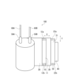
- FIG. 1 is a front view schematically showing an electrode foil for electrolytic capacitors according to an embodiment of the present disclosure
- FIG. 1 is a cross-sectional view schematically showing an electrode foil for electrolytic capacitors according to an embodiment of the present disclosure
- FIG. 1 is a cross-sectional view schematically showing an electrolytic capacitor according to an embodiment of the present disclosure
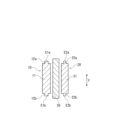
- FIG. It is a perspective view which shows a winding body typically.
- FIG. 3 is a cross-sectional view schematically showing anode foil, cathode foil, and separators that constitute a wound body.
- FIG. 4 is a cross-sectional view schematically showing an electrolytic capacitor according to another embodiment of the present disclosure; It is a top view which shows a laminated body typically.
- FIG. 8 is a cross-sectional view taken along line VIII-VIII of FIG. 7;
- FIG. 1 is a front view showing a metal base sheet prepared in a first step of a method for manufacturing an electrolytic capacitor according to an embodiment of the present disclosure;
- FIG. 4 is a front view showing a metal base sheet having a conductive polymer layer formed on the surface of the first region by a coating process; [ Fig. 4]
- Fig. 4 is a front view showing a metal base sheet having a cut region compressed by a second step of a method for manufacturing an electrolytic capacitor according to an embodiment of the present disclosure.
- An electrolytic capacitor electrode foil includes a metal foil having a first region and a second region other than the first region.
- the second area is an area linearly extending along the edge of the metal foil and is a narrow strip-like area.
- the thickness of the second region is smaller than the thickness of the first region, and a step is provided between the first region and the second region on both surfaces of the metal foil.
- the first region may be strip-shaped.
- Electrode foil (metal foil) is obtained by cutting a metal base sheet into a predetermined size. At this time, burrs are generated at the edges of the electrode foil where the electrode foil is cut.
- the edge of the electrode foil and a member adjacent to the electrode foil (a member that may cause a short circuit due to contact with the electrode foil) when the capacitor element is formed. A large distance can be secured between As a result, even if burrs are present at the edges of the electrode foil, the insulation between the electrode foil and the member can be ensured. As a result, it is possible to suppress an increase in leakage current and the occurrence of short circuits caused by burrs, thereby improving the reliability of the electrolytic capacitor.
- the electrode foil according to the present disclosure may be used for at least one of the anode foil and the cathode foil.
- a large distance can be secured between the edges of the anode foil and the cathode foil, damage to the separator due to burrs can be suppressed, and insulation between the anode foil and the cathode foil can be secured.
- a distance greater than the thickness of the separator can be secured between the edges of the anode foil and the cathode foil, suppressing an increase in leakage current and the occurrence of short circuits even when winding misalignment or winding tightening occurs. can.
- tight winding is a phenomenon in which the separator is compressed due to tensile stress generated during winding, and the distance between the two electrode foils becomes narrower.
- the width of the separator is made larger than the width of the electrode foil in order to prevent contact between the two electrode foils due to winding misalignment. It is also possible to ensure a wider width of , which is advantageous in terms of increasing the capacity.
- the ratio of the area S2 of the second region to the area S1 of the first region when the electrode foil is viewed from the normal direction of the main surface: S2/S1 is, for example, 0.01 or more (or 0.05 or more), or 3 .0 or less, 0.01 or more (or 0.05 or more), or less than 1.0, 0.01 or more (or 0.05 or more), 0.75 or less (or 0 .5 or less).
- the main surface of the electrode foil is the "surface of the first region".
- the width of the second region is, for example, 0.1 mm or more and 10 mm or less (or 7 mm or less).
- the second region is formed by pressing a metal foil and T2/T1 (to be described later) is small (the degree of compression is large), impregnability of the conductive polymer in the second region tends to decrease, which affects the performance of the electrolytic capacitor.
- the area S2 of the second region (the width of the second region) is small.
- the second region is formed, for example, by pressing the edge of the metal foil in the thickness direction of the metal foil. Pressing is performed, for example, by roll-pressing the edges of the metal foil. In this case, the portion that is not pressed becomes the first region.
- T2/T1 which will be described later, can be controlled by the press pressure.
- the ratio of the thickness T2 of the second region to the thickness T1 of the first region: T2/T1 is preferably 0.60 or more and 0.95 or less, more preferably 0.70 or more and 0.90 or less.
- T2/T1 is in the range of 0.60 to 0.95.
- the edge portion of the metal foil includes a first edge portion extending in the longitudinal direction and a second edge portion opposite to the first edge portion.
- the second region is preferably at least one of a second A region linearly extending along the first edge and a second B region linearly extending along the second edge.
- the strip-shaped electrode foil is formed by slitting, and burrs may exist on the first edge and the second edge. Therefore, by using at least one (preferably both) of the 2A region and the 2B region as the second region, it is possible to efficiently suppress the short-circuit failure of the electrolytic capacitor.
- the width and thickness dimensions of the second A region and the second B region may be the same or different.
- the metal foil includes, for example, valve action metals such as aluminum, tantalum, niobium, and titanium.
- the metal foil may contain the valve action metal as an alloy or compound containing the valve action metal.
- the metal foil may be plain foil.
- the metal foil may be a foil having a roughened surface (etching foil), and may have a porous portion on the surfaces of the first region and the second region.
- the metal foil having a roughened surface has a porous portion and a core portion that is continuous with the porous portion, and may be an integral product of the porous portion and the core portion.
- the porous portion is formed by subjecting the surface of the metal foil to etching treatment, and the unetched portion of the metal foil remains as the core portion.
- the thickness of the porous portion is, for example, 1/10 or more and 4/10 or less of the total thickness of the metal foil.
- the porous portion has numerous pits (or pores) surrounded by metal portions.
- the mode pore diameter of the porous portion is, for example, 0.10 ⁇ m or more and 1.0 ⁇ m or less.
- the term "modal pore diameter" as used herein means the most frequent pore diameter (mode diameter) in the volume-based pore diameter distribution measured with a mercury porosimeter.
- the porous portion in the second region preferably has a smaller mode pore size than the porous portion in the first region.
- the second region is less impregnable with the conductive polymer than the first region, which is advantageous in terms of suppressing the occurrence of short circuits due to burrs at the edges of the metal foil.
- the electrode foil having the second region with low impregnability of the conductive polymer is used for at least one of the anode foil and the cathode foil in the wound body, the anode foil and the It is possible to suppress the occurrence of short circuits between the edges of the cathode foil via the conductive polymer.
- the ratio of the mode pore diameter P2 of the porous portion of the second region to the mode pore diameter P1 of the porous portion of the first region: P2/P1 is, for example, 0.3 or more and 0.8 or less (or 0.4 or more and 0.7 or less).
- the most frequent pore diameters P1 and P2 can be obtained by dividing the electrode foil into the first region and the second region and measuring each of them with a mercury porosimeter.
- the porous portion in the second region may have a smaller pit circumference than the porous portion in the first region.
- the “pit circumference length” is the total length of the outline of the pit inner walls included per unit area of the cross section in the thickness direction of the electrode foil (porous portion).
- the ratio of the pit circumference length L2 of the porous portion of the second region to the pit circumference length L1 of the porous portion of the first region: L2/L1 is, for example, 0.70 or more and 0.97 or less (or 0.75 or more and 0.98 or less).
- the above pit circumference length is obtained by the following method.
- a cross-sectional image of the electrode foil (porous portion) in the thickness direction is obtained using a scanning electron microscope (SEM) or a transmission electron microscope (TEM).
- SEM scanning electron microscope
- TEM transmission electron microscope
- Using the cross-sectional image of the porous portion of the first region five regions (area S: 50 ⁇ m 2 to 100 ⁇ m 2 ) within a range from the outer surface of the porous portion to a depth of 1/3 of the thickness of the porous portion.
- the total length L of the contour of the pit inner wall in each region is obtained, and the value (L/S) obtained by dividing the length L by the area S of the region is the pit circumference length of the porous portion of the first region ( ⁇ m/ ⁇ m 2 ).
- An average value of the pit perimeter lengths of the five regions is obtained.
- the pit circumference length of the porous portion in the second region is also obtained in the same manner.
- the porous portion of the second region may have a smaller thickness than the porous portion of the first region.
- the thickness of the porous portion of the second region is set to be greater than the thickness of the porous portion of the first region. can be made smaller.
- the ratio of the thickness TP2 of the porous portion of the second region to the thickness TP1 of the porous portion of the first region: TP2/TP1 is, for example, 0.60 or more and 0.95 or less (or 0.70 or more and 0 .90 or less).
- the thickness TP1 (or thickness TP2) of the porous portion of the first region (or the second region) is determined by any 10 points in the cross section in the thickness direction of the electrode foil (porous portion) of the first region (or the second region). It is obtained by measuring the thickness of and calculating the average value of them.
- the electrode foil may comprise a metal foil having porous portions on the surfaces of the first region and the second region, and a dielectric layer covering the surfaces of the porous portions.
- first electrode foil can be used as an anode foil (or anode body).
- the dielectric layer is formed, for example, by subjecting an etched foil to chemical conversion treatment (anodization).
- the dielectric layer includes an oxide of a valve metal (eg, an oxide of aluminum).
- the dielectric layer is formed along the uneven surface of the porous portion and is formed so as to cover the inner wall surfaces of the pits (or pores) of the porous portion.
- the thickness of the dielectric layer is, for example, 5 nm or more and 300 nm or less.
- the porous portion in the second region preferably has a smaller mode pore size than the first region, and may have a smaller thickness.
- the second region is less impregnable with the conductive polymer than the first region, which is advantageous in terms of suppressing the occurrence of short circuits due to burrs at the edges of the metal foil.
- impregnability of the conductive polymer is low in the second region, and contact between the defective portion of the dielectric layer and the conductive polymer is suppressed, and an increase in leakage current due to the contact is suppressed.
- the dielectric layer thinly covers the surfaces of the porous portions of the first and second regions. Therefore, in the first electrode foil having a dielectric layer on the surface, the ratio of the mode pore diameter PD2 of the porous portion in the second region to the mode pore diameter PD1 of the porous portion in the first region: PD2/PD1 is , is almost equivalent to the above P2/P1.
- the first electrode foil is formed, for example, by forming a porous portion on the surface of a metal foil, forming a dielectric layer covering the surface of the porous portion, and then pressing the metal foil along the edge to form the second electrode foil. Created by forming a region.
- the mode pore size is smaller in the porous portion of the second region than in the porous portion of the first region, and the thickness of the porous portion can also be reduced.
- the electrode foil may comprise a metal foil (plain foil or etched foil) and a coating layer covering the surfaces of the first and second regions of the metal foil.
- the coating layer may include at least one selected from the group consisting of metal oxide layers, metal nitride layers, metal carbide layers, and conductive layers.
- such electrode foil is also referred to as "second electrode foil”.
- the second electrode foil can be used as a cathode foil.
- the coating layer is formed for the purpose of enhancing corrosion resistance, electrical conductivity, and the like. Examples of metals contained in the coating layer include titanium, nickel, tantalum, and niobium.
- the metal contained in the coating layer may be the same as or different from the metal contained in the metal foil.
- the thickness of the coating layer is, for example, 10 nm or more and 5000 nm or less.
- the conductive layer may be a metal layer and/or a carbon layer. Also, carbon may be dispersed in the metal oxide layer, the metal nitride layer, or the conductive layer.
- the covering layer may consist, for example, of a metal oxide layer, a metal nitride layer and/or a metal layer and a carbon layer.
- the second electrode foil is produced, for example, by forming a coating layer on the surface of a metal foil (plain foil or etching foil) and then pressing along the edges of the metal foil to form the second region. be.
- FIG. 1 is a front view schematically showing an electrode foil for an electrolytic capacitor according to one embodiment of the present disclosure.
- FIG. 2 is a cross-sectional view schematically showing an electrode foil for electrolytic capacitors according to an embodiment of the present disclosure.
- the X direction and Y direction indicate the length direction and width direction of the strip-shaped electrode foil, respectively.
- the strip-shaped electrode foil 3 has a first edge E1 and a second edge E2 opposite to the first edge E1.
- the first edge E1 and the second edge E2 are edges extending in the X direction.
- the electrode foil 3 includes a first region 1, a second A region 2a linearly extending along the first edge E1, and a second B region 2b linearly extending along the second edge E2. have.
- the first region 1 has a thickness T1.
- the second A region 2a has a thickness T2.
- the second B region 2b also has substantially the same thickness T2 as the second A region 2a. Thickness T2 of second A region 2a and second B region 2b is smaller than thickness T1 of first region 1 .
- steps are provided between the first region 1 and the second A region 2a and the second B region 2b.
- the electrode foil 3 may be the first electrode foil or the second electrode foil.
- the ratio of the Y-direction length LW2 of the second A region 2a (second B region 2b) to the Y-direction length LW1 of the first region 1: LW2/LW1 is, for example, 0.01 or more (or 0.05 or more). , 3.0 or less, 0.01 or more (or 0.05 or more), or less than 1.0.
- the Y-direction length LW2 of the second A region 2a (the second B region 2b) is, for example, 0.1 mm or more and 10 mm or less (or 7 mm or less).
- the second A region 2a and the second B region 2b have the same thickness and width dimensions, but may have different thickness and/or width dimensions.
- An electrolytic capacitor according to an embodiment of the present disclosure includes a wound capacitor element.
- the capacitor element includes a wound body formed by winding a strip-shaped anode foil, a strip-shaped cathode foil facing the anode foil, and a separator arranged between the anode foil and the cathode foil.
- At least one of the anode foil and the cathode foil includes strip-shaped metal foil having a first region and a second region other than the first region.
- the metal foil has a first edge extending along its length and a second edge opposite to the first edge, and the second region is linear along the first edge. and at least one of a second A region extending linearly along the second edge.
- the thickness of the second region is smaller than the thickness of the first region, and a step is provided between the first region and the second region on both surfaces of the metal foil.
- a wound capacitor element may further include an electrolyte adhering to the wound body.
- An electrolyte is distributed over the dielectric layer and interposed between the anode and cathode foils.
- a wound capacitor element may include a conductive polymer (solid electrolyte) covering a dielectric layer.
- a conductive polymer solid electrolyte covering a dielectric layer.
- the second region is formed by pressing a metal foil, and T2/T1 at that time is relatively large (for example, T2/T1 is greater than 0.70), the conductive polymer is formed in the second region by pressing.
- the influence on the impregnability is kept small, and even if the area S2 of the second region is made relatively large (for example, larger than that of the first region), the performance of the electrolytic capacitor such as capacity is hardly affected.
- T2/T1 is small (for example, T2/T1 is 0.70 or less)
- the impregnation of the conductive polymer in the second region by pressing is greatly affected.
- the ratio of the area S2 of the second region to the area S1 of the first region: S2/S1 is more preferably 0.75 or less (or 0.5 or less), for example. In this case, the influence on the performance of the electrolytic capacitor can be kept small.
- the wound body may be impregnated with a treatment liquid containing a conductive polymer (solution or dispersion of a conductive polymer).
- a treatment liquid containing a conductive polymer may be applied to the surfaces of the electrode foils (anode foil and/or cathode foil) prior to formation.
- the treatment liquid containing the conductive polymer may be applied only to the first region.
- a dispersion containing conductive polymer particles having a diameter larger than the pit diameter of the porous portion of the second region is used as the treatment liquid, and the conductive polymer adheres to the second region (porous portion). You can reduce the amount.
- the anode foil includes a metal foil containing a valve metal and having a porous portion and a core portion continuous with the porous portion, and a dielectric layer covering the surface of the porous portion.
- the thickness of the anode foil is, for example, 60 ⁇ m or more and 200 ⁇ m or less.
- the anode foil is a first electrode foil having a first region and a second region, and the porous portion of the second region preferably has a smaller mode pore diameter than the porous portion of the first region.
- the coverage of the conductive polymer on the inner walls of the pits of the porous portion can be made smaller in the second region than in the first region.
- the ratio of the coverage C2 by the conductive polymer of the porous portion of the second region to the coverage C1 of the conductive polymer of the porous portion of the first region: C2/C1 is, for example, 0.10 or more, 0 0.95 or less (or 0.20 or more and 0.90 or less).
- the coverage of the porous portion with the conductive polymer is obtained by the following method.
- a cross-sectional image in the thickness direction of the electrode foil (porous portion) is obtained using SEM or TEM.
- five regions (area S: 50 ⁇ m 2 to 100 ⁇ m 2 ) within a range from the outer surface of the porous portion to a depth of 1/3 of the thickness of the porous portion.
- the total length L0 of the contours of the pit inner walls in each region and the length L1 of the contours of the portions of the pit inner walls covered with the conductive polymer are obtained, and the ratio (percentage) of L1 to L0 is obtained as the coverage. Calculate the average value of the coverage of the five regions.
- the second area is obtained in the same manner.
- cathode foil A metal foil containing a valve action metal can be used for the cathode foil.
- a plain foil is used as the metal foil, but an etched foil may be used as necessary.
- the cathode foil is preferably the electrode foil described above, and may be the second electrode foil.
- the thickness of the cathode foil is, for example, 20 ⁇ m or more and 60 ⁇ m or less.
- the separator is not particularly limited, and for example, a nonwoven fabric containing fibers of cellulose, polyethylene terephthalate, vinylon, polyamide (eg, aromatic polyamide such as aliphatic polyamide and aramid) may be used.
- a nonwoven fabric containing fibers of cellulose, polyethylene terephthalate, vinylon, polyamide eg, aromatic polyamide such as aliphatic polyamide and aramid
- polyamide eg, aromatic polyamide such as aliphatic polyamide and aramid
- the electrolyte covers at least part of the anode foil (dielectric layer) and is interposed between the anode foil (dielectric layer) and the cathode foil.
- the electrolyte includes at least one of a solid electrolyte and an electrolytic solution.
- a solid electrolyte and an electrolytic solution or a non-aqueous solvent may be used in combination.
- the electrolytic solution and the non-aqueous solvent are collectively referred to as "liquid component".
- the solid electrolyte contains a conductive polymer and may contain a dopant together with the conductive polymer.
- conductive polymers include ⁇ -conjugated polymers.
- conductive polymers include polypyrrole, polythiophene, polyaniline, derivatives thereof, and the like. Derivatives of polythiophene include poly(3,4-ethylenedioxythiophene) and the like.
- Dopants include polystyrene sulfonic acid and the like. The conductive polymer and dopant may be used singly or in combination of two or more.
- the electrolyte contains a non-aqueous solvent and a solute (eg, organic salt) dissolved therein.
- the non-aqueous solvent may be an organic solvent or an ionic liquid.
- a solvent with a high boiling point is preferable as the non-aqueous solvent.
- examples include polyol compounds such as ethylene glycol, sulfone compounds such as sulfolane, lactone compounds such as ⁇ -butyrolactone, ester compounds such as methyl acetate, carbonate compounds such as propylene carbonate, ether compounds such as 1,4-dioxane, and methyl ethyl ketone.
- a ketone compound or the like can be used.
- An organic salt is a salt in which at least one of the anion and cation contains an organic substance.
- organic salts include trimethylamine maleate, triethylamine borodisalicylate, ethyldimethylamine phthalate, mono-1,2,3,4-tetramethylimidazolinium phthalate, mono-1,3-dimethyl-2-phthalate, Ethylimidazolinium and the like may also be used.
- the liquid component may contain an acid component (anion) and a base component (cation).
- a salt may be formed by the acid component and the base component.
- acid components include organic carboxylic acids and inorganic acids.
- inorganic acids include phosphoric acid, boric acid, and sulfuric acid.
- base component include primary to tertiary amine compounds.
- FIG. 3 is a cross-sectional view schematically showing an electrolytic capacitor according to one embodiment of the present disclosure.
- FIG. 4 is a perspective view schematically showing the configuration of the wound body of FIG. 3.
- FIG. 4 the X direction indicates the length direction of strip-shaped anode foil 10 and cathode foil 20
- the Y direction indicates the width direction of anode foil 10 and cathode foil 20 .
- FIG. 5 is a cross-sectional view schematically showing the configuration of anode foil 10, cathode foil 20, and separator 30. As shown in FIG.
- the electrolytic capacitor 200 includes a wound body 100.
- the wound body 100 is constructed by winding an anode foil 10 and a cathode foil 20 with a separator 30 interposed therebetween.
- the wound body 100 has a height Lc.
- the direction of height Lc can also be said to be the Y direction of anode foil 10 and cathode foil 20 .
- the strip-shaped anode foil 10 has a first edge E1a extending in its length direction (X direction) and a second edge E1b opposite to the first edge E1a.
- Anode foil 10 includes first region 11, second A region 12a linearly extending along first edge E1a, and second B region 12b linearly extending along second edge E1b. have.
- the thicknesses of second A region 12a and second B region 12b are each smaller than the thickness of first region 11, and on both surfaces of anode foil 10, between first region 11 and second A region 12a A step is provided, and a step is provided between the first region 11 and the second B region 12b.
- the strip-shaped cathode foil 20 has a first edge E2a extending in its length direction (X direction) and a second edge E2b opposite to the first edge E2a.
- the cathode foil 20 includes a first region 21, a second A region 22a linearly extending along the first edge E2a, and a second B region 22b linearly extending along the second edge E2b. have.
- the thicknesses of the second A region 22a and the second B region 22b are each smaller than the thickness of the first region 21, and on both surfaces of the cathode foil 20, between the first region 21 and the second A region 22a A step is provided, and a step is provided between the first region 21 and the second B region 22b.
- the first edge E1a and the second edge E1b of the anode foil 10 and the second A region 22a and the second B region 22b of the cathode foil 20 By the second A region 12a and the second B region 12b of the anode foil 10 and the second A region 22a and the second B region 22b of the cathode foil 20, the first edge E1a and the second edge E1b of the anode foil 10, and , a large distance between the anode foil 10 and the cathode foil 20 is ensured at the first end edge E2a and the second end edge E2b of the cathode foil 20 .
- the burrs present at the edges of the anode foil and the cathode foil are prevented from breaking through the separators, and the occurrence of short circuits caused by the burrs penetrating the separators is suppressed.
- 2nd A region 12a, 2nd B region 12b, 2nd A region 22a, and 2nd B region 22b provide edge portions E1a and E1b of anode foil 10 and edge portion E2a of cathode foil 20 when wound body 100 is formed.
- E2b a distance equal to or greater than the thickness of the separator 30 can be secured. As a result, it is possible to suppress an increase in leakage current and the occurrence of short-circuit defects even when winding misalignment or winding tightening occurs.
- Lead tabs 50A and 50B are connected to the anode foil 10 and the cathode foil 20, respectively, and the wound body 100 is formed by winding the lead tabs 50A and 50B.
- Lead wires 60A and 60B are connected to the other ends of lead tabs 50A and 50B, respectively.
- a winding stop tape 40 is arranged on the outer surface of the cathode foil 20 located in the outermost layer of the wound body 100 , and the ends of the cathode foil 20 are fixed by the winding stop tape 40 .
- the anode foil 10 is prepared by cutting from a large-sized foil, the rolled body 100 may be further subjected to a chemical conversion treatment in order to provide a dielectric layer on the cut surface.
- the electrolyte adheres to the wound body 100, and is interposed between the anode foil 10 (dielectric layer) and the cathode foil.
- the anode foil 10 dielectric layer
- the cathode foil For example, by impregnating wound body 100 with a treatment liquid containing a conductive polymer, the surface of anode foil 10 (dielectric layer) can be covered with the conductive polymer. Impregnation may be performed under reduced pressure, for example in an atmosphere of 10 kPa to 100 kPa.
- the wound body 100 is housed in the bottomed case 211 so that the lead wires 60A and 60B are located on the opening side of the bottomed case 211.
- metals such as aluminum, stainless steel, copper, iron, and brass, or alloys thereof can be used.
- a sealing member 212 is placed in the opening of the bottomed case 211 in which the wound body 100 is accommodated, and the opening end of the bottomed case 211 is crimped to the sealing member 212 for curling, and the seat plate 213 is attached to the curled portion. By arranging them, the wound body 100 is sealed in the bottomed case 211 .
- the sealing member 212 is formed so that the lead wires 60A and 60B pass therethrough.
- the sealing member 212 may be an insulating material, preferably an elastic material. Among them, highly heat-resistant silicone rubber, fluorine rubber, ethylene propylene rubber, hypalon rubber, butyl rubber, isoprene rubber and the like are preferable.
- An electrolytic capacitor includes a laminate obtained by laminating a plurality of laminated capacitor elements.
- the capacitor element includes a metal foil having a cathode forming portion and an anode lead-out portion extending from one edge portion of the cathode forming portion and having a porous portion on the surface thereof, a dielectric layer covering the cathode forming portion, and a dielectric layer. an overlying cathode portion.
- the cathode forming portion has a first region and a second region other than the first region, and the second region is a line extending along an edge portion other than the one edge portion of the cathode forming portion.
- the second region has a smaller thickness than the first region, and a step is provided between the first region and the second region on both surfaces of the metal foil.
- the cathode section includes, for example, a solid electrolyte layer covering the dielectric layer, and a cathode extraction layer covering the solid electrolyte layer.
- the cathode portions (cathode extraction layers) of adjacent capacitor elements may be in close contact with each other via an adhesive layer formed of a conductive adhesive.
- the laminated portion may be formed by overlapping the ends of the anode lead-out portions of the plurality of capacitor elements.
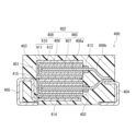
- FIG. 6 is a cross-sectional view schematically showing an electrolytic capacitor according to another embodiment of the present disclosure.
- FIG. 7 is a top view schematically showing a laminate.
- capacitor element 402 first region 461 and second A region 462a to second C region 462c of anode body 460 covered with cathode portion 408 are indicated by dashed lines.
- 8 is a cross-sectional view taken along line VIII-VIII of FIG. 7.
- the electrolytic capacitor 400 includes a laminate 401 , an anode lead terminal 404 and a cathode lead terminal 405 electrically connected to the laminate 401 , and a resin-made exterior body 403 that seals the laminate 401 . A part of the anode lead terminal 404 and the cathode lead terminal 405 is covered with the exterior body 403 .
- the exterior body 403 has a substantially rectangular parallelepiped outer shape, and the electrolytic capacitor 400 also has a substantially rectangular parallelepiped outer shape.
- the laminate 401 is configured by laminating a plurality of capacitor elements 402 .
- Capacitor elements 402 (cathode portions 408) adjacent to each other are electrically connected via an adhesive layer 415 formed of a conductive adhesive.
- an adhesive layer 415 formed of a conductive adhesive.
- two capacitor elements are stacked, but the number of capacitor elements forming the laminate is not limited to this.
- Capacitor element 402 includes metal foil 406 having cathode forming portion 406a and anode lead-out portion 406b extending from one edge (fourth edge E14) of cathode forming portion 406a, and dielectric layer 407 covering cathode forming portion 406a. and a cathode portion 408 covering the dielectric layer 407 .
- Metal foil 406 (cathode forming portion 406 a and anode leading portion 406 b ) has a porous portion on its surface, and dielectric layer 407 is formed to cover the surface of the porous portion of cathode forming portion 406 .
- Cathode formation portion 406 a and dielectric layer 407 constitute anode body 460 .
- the anode body 460 (cathode forming portion 406a) has a first end edge portion E11 to a third end edge portion E13.
- the edges E11-E13 can be formed by cutting.
- Anode body 460 includes first region 461, second A region 462a linearly extending along first edge E11, second B region 462b linearly extending along second edge E12, and second and a second C region 462c linearly extending along the third edge E13.
- Each of the second A region 462a to the second C region 462c has a smaller thickness than the first region 461.
- Steps are provided between the first region 461 and the second A region 462a to the second C region 462c on both surfaces of the anode body 460 (cathode forming portion 406a).
- a second region is formed by the second A region 462a to the second C region 462c.
- the cathode portion solid electrolyte layer, cathode extraction layer
- the cathode portion solid electrolyte layer, cathode extraction layer
- a conductive adhesive is used to bond adjacent capacitor elements together. The bonding is performed by applying a constant pressure to the laminate to bring the capacitor elements into close contact with each other. Therefore, when forming the laminate, pressure may be applied to the capacitor element having burrs.
- pressure may be applied to the capacitor element having burrs when forming an exterior body covering the laminate by injection molding of a resin material, or when heat or vibration is transmitted to the electrolytic capacitor due to reflow processing or the like.
- the burrs covered with the cathode portion press the adjacent capacitor element (dielectric layer), thereby causing defects in the dielectric layer and increasing leakage current. be.
- the burr covered with the cathode portion may break through the dielectric layer of the adjacent capacitor element, causing contact between the cathode portion and the metal substrate of the anode body, resulting in short-circuit failure.
- the edge portions (first edge portions E11 A large distance is ensured between the ⁇ third edge portions E13).
- pressure on the adjacent capacitor element (dielectric layer) due to the burr is suppressed, resulting in an increase in leakage current and occurrence of a short circuit. can be suppressed.
- An insulating separation layer 413 is formed in a portion adjacent to the cathode portion 408 in the anode lead-out portion 406 b to restrict contact between the cathode portion 408 and the anode body 460 .
- the end portions of the plurality of anode lead-out portions 406b are stacked and integrated into one to form a stacked portion.
- the stacked portion of the plurality of anode lead-out portions 406b and the anode lead terminal 404 are electrically connected by welding.
- the cathode portion 408 at the end of the laminate 401 and the cathode lead terminal 405 are electrically connected via an adhesive layer 414 formed of a conductive adhesive.
- the cathode section 408 includes a solid electrolyte layer 409 covering the dielectric layer 407 and a cathode extraction layer 410 covering the solid electrolyte layer 409 .
- Cathode extraction layer 410 has carbon layer 411 and silver paste layer 412 .
- the carbon layer 411 contains, for example, carbon particles and silver.
- Silver paste layer 412 includes, for example, silver particles and a binder.
- the binder is not particularly limited, a cured product of a curable resin is preferable.
- curable resins include thermosetting resins such as epoxy resins.
- the solid electrolyte layer 409 contains a conductive polymer, and may contain a dopant or the like as necessary.
- conductive polymers examples include polypyrrole, polythiophene, polyaniline, and derivatives thereof.
- Solid electrolyte layer 409 is formed by, for example, coating or impregnating the surface of anode body 460 having a first region and a second region with a treatment liquid containing a conductive polymer (solution or dispersion of a conductive polymer). can be formed.
- a treatment liquid containing a conductive polymer may be applied only to the first region 461 to form a solid electrolyte layer, thereby forming a cathode portion.
- the exterior body 403 preferably contains a cured product of a curable resin composition, and may contain a thermoplastic resin or a composition containing it.
- curable resins include thermosetting resins such as epoxy resins.
- a manufacturing method of an electrolytic capacitor includes a first step, a second step (pressing step), and a third step (cutting step).
- a metal substrate sheet having a plurality of first regions and a plurality of cutting regions alternately arranged in stripes is prepared.
- the cut area is compressed in the thickness direction of the metal base sheet.
- the widthwise central portion of the cut area is cut along the length direction of the cut area to obtain a plurality of electrode foils.
- the width of the cutting area is preferably smaller than the width of the first area.
- the metal base sheet may be a plain foil or an etched foil.
- the metal substrate sheet may be a sheet having a dielectric layer on its surface, or a sheet having a coating layer on its surface.
- the metal base sheet prepared in the first step contains a valve action metal.
- a metal base sheet having a dielectric layer on its surface may be prepared.
- the first step may include a step of roughening the surface of the metal substrate sheet to form a porous portion.
- the first step may include forming a dielectric layer covering the surface of the porous portion.
- the electrode foil obtained in the third step can be used as the anode foil.
- the cut area of the metal base sheet is roll-pressed.
- a strip-shaped metal substrate sheet with a width of 10 mm or more and 500 mm or less is slit into widths of 2 mm or more and 100 mm or less to obtain a plurality of strip-shaped electrode foils.
- a device equipped with rolls for conveying the metal base sheet, rolling rolls and slitting blades provided on the conveying path may be used.
- the mill rolls and blades are arranged respectively upstream and downstream of the conveying path.
- a plurality of rolling rolls and blades are arranged at regular intervals at positions corresponding to a plurality of cutting areas.
- the pressing and slitting of a plurality of cutting regions can be performed at once by a plurality of rolling rolls and blades, the positioning of the pressing and slitting is easy, and the second and third steps can be performed efficiently. can be done.
- the manufacturing method may include a step of applying a treatment liquid containing a conductive polymer to the first region of the metal base sheet (application step).
- a step of applying a treatment liquid containing a conductive polymer to a first region of a metal base sheet having a dielectric layer on its surface is performed to form a conductive polymer layer (solid electrolyte layer) covering the surface of the dielectric layer.
- the coating step is preferably performed after the second step and before the third step, and may be performed before the second step.
- a coating method such as gravure coating is used.
- the second region may not be coated with the treatment liquid containing the conductive polymer.
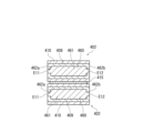
- FIG. 9 is a front view showing a metal substrate sheet prepared in the first step.
- FIG. 10 is a front view showing a metal substrate sheet having a conductive polymer layer formed on the surface of the first region.
- FIG. 11 is a front view showing a metal base sheet with a compressed cut area. 10 and 11, hatched areas indicate areas where the conductive polymer layer is formed.
- a sheet 300 (metal base sheet) shown in FIG. 9 has a plurality of first regions 301 and a plurality of cutting regions 302 alternately arranged in stripes.
- cut areas 302 of the same width are provided at regular intervals.
- the width of the cutting area 302 is narrower than the width of the first area 301 .
- the compressed area 312 shown in FIG. 11 is formed.
- the second region A plurality of strip-shaped electrode foils having
- a strip-shaped anode foil and a strip-shaped cathode foil are wound in the length direction of the anode foil and the cathode foil with a separator interposed between the anode foil and the cathode foil.
- a step of obtaining a body may be included.
- At least one of the anode foil and the cathode foil may be an electrode foil obtained by the above manufacturing method (including the first to third steps and, if necessary, a coating step).
- the manufacturing method may include a step of impregnating the wound body with a treatment liquid containing a conductive polymer.
- a treatment liquid containing a conductive polymer When the coating step is not performed, it is desirable to perform the step of impregnating the wound body.
- a metal substrate sheet (thickness 100 ⁇ m) having a plurality of first regions (5.0 mm wide) and a plurality of cut regions (0.3 mm wide) alternately arranged in stripes was prepared (first step).
- Etched foil with a dielectric layer on the surface was used for the metal base sheet.
- the etched foil was obtained by etching an Al foil having a thickness of 100 ⁇ m to form a porous portion (thickness per side: 35 ⁇ m, mode pore diameter: 0.15 ⁇ m) on the surface of the Al foil.
- the dielectric layer was obtained by chemically converting the etched foil to form an aluminum oxide layer (thickness 70 nm).
- a plurality of belt-shaped anode foils were obtained by cutting the central portion of the cut region in the width direction along the length direction of the cut region (third step).
- the anode foil has a first region (thickness T1: 100 ⁇ m), a second A region linearly extending along the first edge, and a second B region linearly extending along the second edge. had.
- the thickness T2 of the 2nd A region and the 2nd B region was the value shown in Table 1.
- the width dimension of the first region (the length in the Y direction of the first region 1 in FIG. 1) was 5.0 mm.
- the width dimension of the 2A region and the 2B region (length in the Y direction of the 2A region 2a and the 2B region 2b in FIG. 1) was 0.15 mm.
- an etching foil having a chemical conversion film on its surface and cut into a predetermined size was used as the cathode foil.
- the etching foil was obtained by etching an Al foil having a thickness of 50 ⁇ m to form a porous portion (thickness per side: 15 ⁇ m, mode pore diameter: 0.12 ⁇ m) on the surface of the Al foil.
- the chemical conversion coating was obtained by subjecting the etched foil to chemical conversion treatment to form an aluminum oxide layer (thickness: 5 nm).
- An anode lead tab and a cathode lead tab to which lead wires were connected were connected to the prepared anode foil and cathode foil, respectively. Then, the anode foil and the cathode foil were wound with a separator sandwiched therebetween, and the outer surfaces were fixed with a winding stop tape. Thus, a wound body was produced.
- the anode foil was chemically treated again to form a dielectric layer on the end surface of the anode foil.
- the capacitor element After housing the capacitor element in the bottomed case, the capacitor element was impregnated with the electrolytic solution at room temperature under atmospheric pressure.
- the electrolytic solution a solution containing triethylamine phthalate dissolved in ethylene glycol as a main component was used.
- a sealing member and a seat plate were placed in the opening of the bottomed case to seal the capacitor element.
- an electrolytic capacitor was completed.
- an aging treatment was performed at 105° C. for 2 hours while applying a rated voltage.
- A1 to A6 in Table 1 indicate the electrolytic capacitors of Examples 1 to 6, respectively.
- Table 1 shows the evaluation results.
- the distance between the edge portions of the anode foil and the cathode foil was increased, and damage to the separator due to burrs present at the edge portions of the electrode foils was suppressed.
- the initial LC defect rate was small, and the leakage current after vibration was also small.
- burrs existing at the edges of the electrode foil increased the initial LC defect rate and increased the leakage current after vibration.
- an etching foil having a dielectric layer on its surface and cut into a predetermined size was used as the anode foil.
- the etched foil was obtained by etching an Al foil having a thickness of 100 ⁇ m to form a porous portion (thickness per side: 35 ⁇ m, mode pore diameter: 0.15 ⁇ m) on the surface of the Al foil.
- the dielectric layer was obtained by chemically converting the etched foil to form an aluminum oxide layer (thickness 70 nm).
- a metal substrate sheet having a plurality of first regions (50 ⁇ m thick, 5.0 mm wide) and a plurality of cut regions (50 ⁇ m thick, 0.3 mm wide) alternately arranged in stripes was prepared (first step).
- the metal base sheet An etched foil with a chemical conversion film on the surface was used as the metal base sheet.
- the etching foil was obtained by etching an Al foil having a thickness of 50 ⁇ m to form a porous portion (thickness per side: 15 ⁇ m, mode pore diameter: 0.12 ⁇ m) on the surface of the Al foil.
- the chemical conversion coating was obtained by subjecting the etched foil to chemical conversion treatment to form an aluminum oxide layer (thickness: 5 nm).
- a plurality of band-shaped cathode foils were obtained by cutting the center portion of the cut region in the width direction along the length direction of the cut region (third step).
- the cathode foil has a first region (thickness T1: 50 ⁇ m), a second A region linearly extending along the first edge, and a second B region linearly extending along the second edge. had.
- the thickness T2 of the 2nd A region and the 2nd B region was the value shown in Table 1.
- the width dimension of the first region (the length in the Y direction of the first region 1 in FIG. 1) was 5.0 mm.
- the width dimension of the 2A region and the 2B region (length in the Y direction of the 2A region 2a and the 2B region 2b in FIG. 1) was 0.15 mm.
- Electrolytic capacitors A7 to A12 were produced in the same manner as in Example 1, except that the anode foil prepared above and the cathode foil obtained above were used.
- Evaluation 1 and Evaluation 2 above were performed for electrolytic capacitors A7 to A12.
- Table 2 shows the evaluation results.
- Table 2 also shows the evaluation results of the electrolytic capacitor B1.
- the distance between the edges of the anode foil and the cathode foil was increased, and damage to the separator due to burrs present at the edges of the electrode foils was suppressed.
- the electrolytic capacitors A7 to A12 had a smaller initial LC defect rate and a smaller leakage current after vibration than the electrolytic capacitor B1.
- the electrode foil according to the present disclosure is suitable for use in electrolytic capacitors that require high reliability.
Landscapes
- Engineering & Computer Science (AREA)
- Power Engineering (AREA)
- Microelectronics & Electronic Packaging (AREA)
- Chemical & Material Sciences (AREA)
- Chemical Kinetics & Catalysis (AREA)
- Electrochemistry (AREA)
- Fixed Capacitors And Capacitor Manufacturing Machines (AREA)
Abstract
This electrolytic capacitor-use electrode foil includes a metal foil having a first region and a second region other than the first region. The second region extends linearly along the end edges of the metal foil. The thickness of the second region is less than the thickness of the first region. On both surfaces of the metal foil, a step is provided between the first region and the second region.
Description
本開示は、電解コンデンサ用電極箔、電解コンデンサ、および電解コンデンサの製造方法に関する。
The present disclosure relates to electrode foils for electrolytic capacitors, electrolytic capacitors, and methods of manufacturing electrolytic capacitors.
電解コンデンサは、例えば、巻回体を備える。巻回体は、帯状の陽極箔、陽極箔に対向する帯状の陰極箔、および陽極箔と陰極箔との間に配されるセパレータを巻回して構成される(例えば、特許文献1)。
An electrolytic capacitor, for example, includes a wound body. The wound body is configured by winding a strip-shaped anode foil, a strip-shaped cathode foil facing the anode foil, and a separator arranged between the anode foil and the cathode foil (for example, Patent Document 1).
電極箔は、通常、所定のサイズに裁断して用いられ、裁断時にバリが生じやすい。当該バリを有する電極箔を用いると、電解コンデンサの信頼性が低下する。例えば、巻回体を備える電解コンデンサでは、バリがセパレータを突き破り、ショート不良の発生を招くことがある。
Electrode foil is usually cut to a predetermined size before use, and burrs are likely to occur during cutting. The use of electrode foils having such burrs reduces the reliability of electrolytic capacitors. For example, in an electrolytic capacitor with a wound body, a burr may break through the separator and cause a short circuit.
本開示の一側面は、第1領域および前記第1領域以外の第2領域を有する金属箔を含み、前記第2領域は、前記金属箔の端縁部に沿って線状に延びる領域であり、前記第2領域の厚みは、前記第1領域の厚みよりも小さくなっており、前記金属箔の両方の表面において、前記第1領域と前記第2領域との間に段差が設けられている、電解コンデンサ用電極箔に関する。
One aspect of the present disclosure includes a metal foil having a first region and a second region other than the first region, wherein the second region is a region linearly extending along an edge of the metal foil. , the thickness of the second region is smaller than the thickness of the first region, and a step is provided between the first region and the second region on both surfaces of the metal foil. , relating to electrode foils for electrolytic capacitors.
本開示の他の側面は、巻回型のコンデンサ素子を備え、前記コンデンサ素子は、帯状の陽極箔、帯状の陰極箔、および前記陽極箔と前記陰極箔との間に配されるセパレータを巻回して構成される巻回体を備え、前記陽極箔および前記陰極箔の少なくとも一方は、第1領域および前記第1領域以外の第2領域を有する帯状の金属箔を含み、前記金属箔は、その長さ方向に延びる第1端縁部および前記第1端縁部と反対側の第2端縁部を有し、前記第2領域は、前記第1端縁部に沿って線状に延びる第2A領域、および、前記第2端縁部に沿って線状に延びる第2B領域の少なくとも一方であり、前記第2領域の厚みは、前記第1領域の厚みよりも小さくなっており、前記金属箔の両方の表面において、前記第1領域と前記第2領域との間に段差が設けられている、電解コンデンサに関する。
Another aspect of the present disclosure includes a wound capacitor element, the capacitor element winding a strip-shaped anode foil, a strip-shaped cathode foil, and a separator disposed between the anode foil and the cathode foil. At least one of the anode foil and the cathode foil includes a strip-shaped metal foil having a first region and a second region other than the first region, the metal foil comprising: It has a first edge extending along its length and a second edge opposite said first edge, said second region extending linearly along said first edge. and at least one of a second A region and a second B region linearly extending along the second edge, wherein the thickness of the second region is smaller than the thickness of the first region, and The present invention relates to an electrolytic capacitor in which steps are provided between the first region and the second region on both surfaces of a metal foil.
本開示の更に他の側面は、積層型のコンデンサ素子を複数積層した積層体を備え、前記コンデンサ素子は、陰極形成部および前記陰極形成部の一端縁部より延びる陽極引出部を有するとともに、表面に多孔質部を有する金属箔と、前記陰極形成部を覆う誘電体層と、前記誘電体層を覆う陰極部と、を備え、前記陰極形成部は、第1領域と、前記第1領域以外の第2領域と、を有し、前記第2領域は、前記陰極形成部における前記一端縁部以外の他の端縁部に沿って線状に延びる領域であり、前記第2領域は、前記第1領域よりも厚みが小さくなっており、前記金属箔の両方の表面において、前記第1領域と前記第2領域との間に段差が設けられている、電解コンデンサに関する。
Still another aspect of the present disclosure includes a laminate in which a plurality of laminated capacitor elements are laminated, the capacitor element having a cathode formation portion and an anode lead-out portion extending from one edge portion of the cathode formation portion, and a surface a metal foil having a porous portion in it, a dielectric layer covering the cathode forming portion, and a cathode portion covering the dielectric layer, wherein the cathode forming portion includes a first region and a portion other than the first region and a second region, wherein the second region is a region linearly extending along an edge portion other than the one edge portion of the cathode forming portion, and the second region is the The present invention relates to an electrolytic capacitor having a thickness smaller than that of a first region and having a step between the first region and the second region on both surfaces of the metal foil.
本開示の更に他の側面は、複数の第1領域および複数の切断領域を交互にストライプ状に有する金属基材シートを準備する第1工程と、前記切断領域を前記金属基材シートの厚み方向に圧縮する第2工程と、前記切断領域の幅方向の中央部を前記切断領域の長さ方向に沿って切断し、複数の電極箔を得る第3工程と、を含む、電解コンデンサの製造方法に関する。
Still another aspect of the present disclosure includes a first step of preparing a metal base sheet having a plurality of first regions and a plurality of cut regions alternately arranged in stripes; and a third step of obtaining a plurality of electrode foils by cutting the center portion of the cut region in the width direction along the length direction of the cut region. Regarding.
本開示によれば、電解コンデンサの信頼性の低下を抑制することができる。
According to the present disclosure, deterioration in reliability of electrolytic capacitors can be suppressed.
本発明の新規な特徴を添付の請求の範囲に記述するが、本発明は、構成および内容の両方に関し、本発明の他の目的および特徴と併せ、図面を照合した以下の詳細な説明によりさらによく理解されるであろう。
While the novel features of the present invention are set forth in the appended claims, the present invention, both as to construction and content, together with other objects and features of the present invention, will be further developed by the following detailed description in conjunction with the drawings. will be well understood.
以下では、本開示の実施形態について例を挙げて説明するが、本開示は以下で説明する例に限定されない。以下の説明では、具体的な数値や材料を例示する場合があるが、本開示の効果が得られる限り、他の数値や材料を適用してもよい。この明細書において、「数値A~数値B」という記載は、数値Aおよび数値Bを含み、「数値A以上で数値B以下」と読み替えることが可能である。以下の説明において、特定の物性や条件などに関する数値の下限と上限とを例示した場合、下限が上限以上とならない限り、例示した下限のいずれかと例示した上限のいずれかを任意に組み合わせることができる。複数の材料が例示される場合、その中から1種を選択して単独で用いてもよく、2種以上を組み合わせて用いてもよい。
The embodiments of the present disclosure will be described below with examples, but the present disclosure is not limited to the examples described below. In the following description, specific numerical values and materials may be exemplified, but other numerical values and materials may be applied as long as the effects of the present disclosure can be obtained. In this specification, the description "numerical value A to numerical value B" includes numerical value A and numerical value B, and can be read as "numerical value A or more and numerical value B or less". In the following description, when lower and upper limits of numerical values relating to specific physical properties, conditions, etc. are exemplified, any of the illustrated lower limits and any of the illustrated upper limits can be arbitrarily combined as long as the lower limit is not greater than or equal to the upper limit. . When a plurality of materials are exemplified, one of them may be selected and used alone, or two or more may be used in combination.
[電解コンデンサ用電極箔]
本開示の実施形態に係る電解コンデンサ用電極箔は、第1領域および第1領域以外の第2領域を有する金属箔を含む。第2領域は、金属箔の端縁部に沿って線状に延びる領域であり、幅の狭いストリップ(strip)状の領域である。第2領域の厚みは第1領域の厚みよりも小さくなっており、金属箔の両方の表面において、第1領域と第2領域との間に段差が設けられている。第1領域は帯状であってもよい。 [Electrode foil for electrolytic capacitors]
An electrolytic capacitor electrode foil according to an embodiment of the present disclosure includes a metal foil having a first region and a second region other than the first region. The second area is an area linearly extending along the edge of the metal foil and is a narrow strip-like area. The thickness of the second region is smaller than the thickness of the first region, and a step is provided between the first region and the second region on both surfaces of the metal foil. The first region may be strip-shaped.
電極箔(金属箔)は、金属基材シートを所定のサイズに裁断して得られる。このとき、裁断箇所である電極箔の端縁部にバリが生じる。電極箔の端縁部に第2領域を設けることにより、コンデンサ素子の構成時に、電極箔の端縁部と、当該電極箔に隣接する部材(当該電極箔との接触によりショートを生じ得る部材)との間の距離を大きく確保できる。これにより、電極箔の端縁部にバリが存在する場合でも、当該電極箔と当該部材との間の絶縁性を確保できる。その結果、バリに起因する漏れ電流の増大やショート不良の発生を抑制でき、電解コンデンサの信頼性が向上する。
Electrode foil (metal foil) is obtained by cutting a metal base sheet into a predetermined size. At this time, burrs are generated at the edges of the electrode foil where the electrode foil is cut. By providing the second region at the edge of the electrode foil, the edge of the electrode foil and a member adjacent to the electrode foil (a member that may cause a short circuit due to contact with the electrode foil) when the capacitor element is formed. A large distance can be secured between As a result, even if burrs are present at the edges of the electrode foil, the insulation between the electrode foil and the member can be ensured. As a result, it is possible to suppress an increase in leakage current and the occurrence of short circuits caused by burrs, thereby improving the reliability of the electrolytic capacitor.
巻回体を備える電解コンデンサの場合、陽極箔および陰極箔の少なくとも一方に本開示に係る電極箔を用いればよい。これにより、陽極箔および陰極箔の端縁部間の距離を大きく確保でき、バリによるセパレータの損傷が抑制され、陽極箔と陰極箔との間の絶縁性を確保できる。また、巻回体の構成時に陽極箔および陰極箔の端縁部間でセパレータの厚み以上の距離を確保でき、巻ずれや巻締まりが生じる場合でも、漏れ電流の増大やショート不良の発生を抑制できる。なお、巻締まりとは、巻回時に生じる引張応力により、セパレータが圧縮され、両極箔間の距離が狭くなる現象である。また、巻ずれによる両極箔同士の接触を防ぐため、セパレータの幅は電極箔の幅よりも大きくしているが、本開示に係る電極箔を用いる場合、セパレータの幅をより小さくでき、電極箔の幅をより大きく確保することもでき、大容量化の面で有利である。
In the case of an electrolytic capacitor with a wound body, the electrode foil according to the present disclosure may be used for at least one of the anode foil and the cathode foil. As a result, a large distance can be secured between the edges of the anode foil and the cathode foil, damage to the separator due to burrs can be suppressed, and insulation between the anode foil and the cathode foil can be secured. In addition, when forming a wound body, a distance greater than the thickness of the separator can be secured between the edges of the anode foil and the cathode foil, suppressing an increase in leakage current and the occurrence of short circuits even when winding misalignment or winding tightening occurs. can. It should be noted that tight winding is a phenomenon in which the separator is compressed due to tensile stress generated during winding, and the distance between the two electrode foils becomes narrower. In addition, the width of the separator is made larger than the width of the electrode foil in order to prevent contact between the two electrode foils due to winding misalignment. It is also possible to ensure a wider width of , which is advantageous in terms of increasing the capacity.
電極箔をその主面の法線方向からみたとき、第1領域の面積S1に対する第2領域の面積S2の比:S2/S1は、例えば、0.01以上(もしくは0.05以上)、3.0以下であってもよく、0.01以上(もしくは0.05以上)、1.0未満であってもよく、0.01以上(もしくは0.05以上)、0.75以下(もしくは0.5以下)であってもよい。なお、電極箔の主面とは、「第1領域の表面」である。第2領域の幅は、例えば、0.1mm以上、10mm以下(もしくは7mm以下)である。第2領域が金属箔のプレスにより形成され、後述のT2/T1が小さい(圧縮度合いが大きい)場合、第2領域では導電性高分子の含浸性が低下しやすく、それによる電解コンデンサの性能への影響を小さく抑えるために、第2領域の面積S2(第2領域の幅)は小さいことが望ましい。
The ratio of the area S2 of the second region to the area S1 of the first region when the electrode foil is viewed from the normal direction of the main surface: S2/S1 is, for example, 0.01 or more (or 0.05 or more), or 3 .0 or less, 0.01 or more (or 0.05 or more), or less than 1.0, 0.01 or more (or 0.05 or more), 0.75 or less (or 0 .5 or less). The main surface of the electrode foil is the "surface of the first region". The width of the second region is, for example, 0.1 mm or more and 10 mm or less (or 7 mm or less). When the second region is formed by pressing a metal foil and T2/T1 (to be described later) is small (the degree of compression is large), impregnability of the conductive polymer in the second region tends to decrease, which affects the performance of the electrolytic capacitor. In order to suppress the influence of , it is desirable that the area S2 of the second region (the width of the second region) is small.
第2領域は、例えば、金属箔の端縁部を金属箔の厚み方向にプレスすることにより形成される。プレスは、例えば、金属箔の端縁部をロールプレスすることにより行われる。この場合、プレスしない部分が第1領域となる。後述のT2/T1は、プレス圧により制御できる。
The second region is formed, for example, by pressing the edge of the metal foil in the thickness direction of the metal foil. Pressing is performed, for example, by roll-pressing the edges of the metal foil. In this case, the portion that is not pressed becomes the first region. T2/T1, which will be described later, can be controlled by the press pressure.
第1領域の厚みT1に対する第2領域の厚みT2の比:T2/T1は、好ましくは0.60以上、0.95以下であり、より好ましくは0.70以上、0.90以下である。表面に誘電体層(もしくは被覆層)を有する金属箔の端縁部をプレスして第2領域を形成する際に、T2/T1が0.60以上、0.95以下の範囲内となるようにプレス圧を調節する場合、第1領域と第2領域の段差において金属箔の金属組織の露出が抑えられ、当該段差も誘電体層(もしくは被覆層)で覆われやすい。
The ratio of the thickness T2 of the second region to the thickness T1 of the first region: T2/T1 is preferably 0.60 or more and 0.95 or less, more preferably 0.70 or more and 0.90 or less. When the edge of the metal foil having a dielectric layer (or coating layer) on the surface is pressed to form the second region, T2/T1 is in the range of 0.60 to 0.95. When the pressing pressure is adjusted to , exposure of the metal structure of the metal foil is suppressed at the step between the first and second regions, and the step is easily covered with the dielectric layer (or coating layer).
金属箔が帯状である場合、金属箔の端縁部は、その長さ方向に延びる第1端縁部および第1端縁部と反対側の第2端縁部を含む。この場合、第2領域は、第1端縁部に沿って線状に延びる第2A領域、および、第2端縁部に沿って線状に延びる第2B領域の少なくとも一方であることが好ましい。帯状の電極箔はスリット加工により形成され、第1端縁部および第2端縁部にバリが存在し得る。よって、第2A領域および第2B領域の少なくとも一方(好ましくは両方)を第2領域とすることで、電解コンデンサのショート不良などを効率的に抑制できる。第2A領域および第2B領域により第2領域が形成される場合、第2A領域および第2B領域の幅および厚みの寸法は、互いに同じであってもよく、異なっていてもよい。
When the metal foil is strip-shaped, the edge portion of the metal foil includes a first edge portion extending in the longitudinal direction and a second edge portion opposite to the first edge portion. In this case, the second region is preferably at least one of a second A region linearly extending along the first edge and a second B region linearly extending along the second edge. The strip-shaped electrode foil is formed by slitting, and burrs may exist on the first edge and the second edge. Therefore, by using at least one (preferably both) of the 2A region and the 2B region as the second region, it is possible to efficiently suppress the short-circuit failure of the electrolytic capacitor. When the second region is formed by the second A region and the second B region, the width and thickness dimensions of the second A region and the second B region may be the same or different.
金属箔は、例えば、アルミニウム、タンタル、ニオブ、チタンなどの弁作用金属を含む。金属箔は、弁作用金属を、当該弁作用金属を含む合金または化合物として含んでもよい。
The metal foil includes, for example, valve action metals such as aluminum, tantalum, niobium, and titanium. The metal foil may contain the valve action metal as an alloy or compound containing the valve action metal.
金属箔は、プレーン箔であってもよい。また、金属箔は、表面が粗面化された箔(エッチング箔)であってもよく、第1領域および第2領域の表面に多孔質部を有してもよい。表面が粗面化された金属箔は、多孔質部と、多孔質部に連続している芯部とを有し、多孔質部と芯部との一体化物であってもよい。多孔質部は、金属箔の表面にエッチング処理を施すことにより形成され、金属箔のエッチングされない部分は芯部として残る。多孔質部の厚み(片面あたりの厚み)は、例えば、金属箔の総厚みの1/10以上、4/10以下である。多孔質部は金属部分で囲まれる多数のピット(もしくは細孔)を有する。多孔質部の最頻細孔径は、例えば、0.10μm以上、1.0μm以下である。なお、ここでいう最頻細孔径とは、水銀ポロシメータで測定される体積基準の細孔径分布の最頻細孔径(モード径)を意味する。
The metal foil may be plain foil. Moreover, the metal foil may be a foil having a roughened surface (etching foil), and may have a porous portion on the surfaces of the first region and the second region. The metal foil having a roughened surface has a porous portion and a core portion that is continuous with the porous portion, and may be an integral product of the porous portion and the core portion. The porous portion is formed by subjecting the surface of the metal foil to etching treatment, and the unetched portion of the metal foil remains as the core portion. The thickness of the porous portion (thickness per side) is, for example, 1/10 or more and 4/10 or less of the total thickness of the metal foil. The porous portion has numerous pits (or pores) surrounded by metal portions. The mode pore diameter of the porous portion is, for example, 0.10 μm or more and 1.0 μm or less. The term "modal pore diameter" as used herein means the most frequent pore diameter (mode diameter) in the volume-based pore diameter distribution measured with a mercury porosimeter.
第2領域の多孔質部は、第1領域の多孔質部よりも最頻細孔径が小さいことが好ましい。この場合、第2領域は第1領域よりも導電性高分子の含浸性が低く、金属箔の端縁部のバリに起因するショート不良の発生などの抑制の面で有利である。また、導電性高分子の含浸性が低い第2領域を有する電極箔を、巻回体における陽極箔および陰極箔の少なくとも一方に用いる場合、巻回体の構成時の巻きずれによる、陽極箔および陰極箔の端縁部間での導電性高分子を介したショート不良の発生を抑制できる。
The porous portion in the second region preferably has a smaller mode pore size than the porous portion in the first region. In this case, the second region is less impregnable with the conductive polymer than the first region, which is advantageous in terms of suppressing the occurrence of short circuits due to burrs at the edges of the metal foil. Further, when the electrode foil having the second region with low impregnability of the conductive polymer is used for at least one of the anode foil and the cathode foil in the wound body, the anode foil and the It is possible to suppress the occurrence of short circuits between the edges of the cathode foil via the conductive polymer.
第1領域の多孔質部の最頻細孔径P1に対する、第2領域の多孔質部の最頻細孔径P2の比:P2/P1は、例えば、0.3以上、0.8以下(もしくは、0.4以上、0.7以下)である。最頻細孔径P1およびP2は、電極箔を第1領域および第2領域に分割し、それぞれについて水銀ポロシメータによる測定を行えばよい。
The ratio of the mode pore diameter P2 of the porous portion of the second region to the mode pore diameter P1 of the porous portion of the first region: P2/P1 is, for example, 0.3 or more and 0.8 or less (or 0.4 or more and 0.7 or less). The most frequent pore diameters P1 and P2 can be obtained by dividing the electrode foil into the first region and the second region and measuring each of them with a mercury porosimeter.
第2領域の多孔質部は、第1領域の多孔質部よりもピット周囲長さが小さくなっていてもよい。「ピット周囲長さ」とは、電極箔(多孔質部)の厚み方向の断面の単位面積あたりに内包するピット内壁の輪郭の合計長さである。第2領域がプレスにより形成される場合、第2領域は第1領域よりもピット周囲長さが大きく、ピット径が小さい傾向がある。第1領域の多孔質部のピット周囲長さL1に対する、第2領域の多孔質部のピット周囲長さL2の比:L2/L1は、例えば、0.70以上、0.97以下(もしくは、0.75以上、0.98以下)である。
The porous portion in the second region may have a smaller pit circumference than the porous portion in the first region. The “pit circumference length” is the total length of the outline of the pit inner walls included per unit area of the cross section in the thickness direction of the electrode foil (porous portion). When the second region is formed by pressing, the second region tends to have a longer pit circumference and a smaller pit diameter than the first region. The ratio of the pit circumference length L2 of the porous portion of the second region to the pit circumference length L1 of the porous portion of the first region: L2/L1 is, for example, 0.70 or more and 0.97 or less (or 0.75 or more and 0.98 or less).
上記のピット周囲長さは、以下の方法により求められる。
走査型電子顕微鏡(SEM)または透過型電子顕微鏡(TEM)を用いて電極箔(多孔質部)の厚み方向の断面画像を得る。第1領域の多孔質部の断面画像を用い、多孔質部の外表面から多孔質部の厚みの1/3の深さまでの範囲内において5つの領域(面積S:50μm2~100μm2)を任意に選出する。各領域内のピット内壁の輪郭の合計長さLを求め、当該長さLを当該領域の面積Sで除した値(L/S)を、第1領域の多孔質部のピット周囲長さ(μm/μm2)として求める。5つの領域のピット周囲長さの平均値を求める。第2領域の多孔質部のピット周囲長さについても、同様にして求める。 The above pit circumference length is obtained by the following method.
A cross-sectional image of the electrode foil (porous portion) in the thickness direction is obtained using a scanning electron microscope (SEM) or a transmission electron microscope (TEM). Using the cross-sectional image of the porous portion of the first region, five regions (area S: 50 μm 2 to 100 μm 2 ) within a range from the outer surface of the porous portion to a depth of 1/3 of the thickness of the porous portion. Select arbitrarily. The total length L of the contour of the pit inner wall in each region is obtained, and the value (L/S) obtained by dividing the length L by the area S of the region is the pit circumference length of the porous portion of the first region ( μm/μm 2 ). An average value of the pit perimeter lengths of the five regions is obtained. The pit circumference length of the porous portion in the second region is also obtained in the same manner.
第2領域の多孔質部は、第1領域の多孔質部よりも厚みが小さくてもよい。表面に多孔質部を有する金属箔(エッチング箔)の端縁部をプレスして第2領域を形成する場合、第2領域の多孔質部の厚みを、第1領域の多孔質部の厚みよりも小さくできる。第1領域の多孔質部の厚みTP1に対する、第2領域の多孔質部の厚みTP2の比:TP2/TP1は、例えば、0.60以上、0.95以下(もしくは、0.70以上、0.90以下)である。
The porous portion of the second region may have a smaller thickness than the porous portion of the first region. When the edge of a metal foil (etching foil) having a porous portion on its surface is pressed to form the second region, the thickness of the porous portion of the second region is set to be greater than the thickness of the porous portion of the first region. can be made smaller. The ratio of the thickness TP2 of the porous portion of the second region to the thickness TP1 of the porous portion of the first region: TP2/TP1 is, for example, 0.60 or more and 0.95 or less (or 0.70 or more and 0 .90 or less).
第1領域(もしくは第2領域)の多孔質部の厚みTP1(もしくは厚みTP2)は、第1領域(もしくは第2領域)の電極箔(多孔質部)の厚み方向の断面における任意の10点の厚みを測定し、それらの平均値を算出することにより求められる。
The thickness TP1 (or thickness TP2) of the porous portion of the first region (or the second region) is determined by any 10 points in the cross section in the thickness direction of the electrode foil (porous portion) of the first region (or the second region). It is obtained by measuring the thickness of and calculating the average value of them.
電極箔は、第1領域および第2領域の表面に多孔質部を有する金属箔と、多孔質部の表面を覆う誘電体層と、を備えてもよい。以下、このような電極箔を、「第1電極箔」とも称する。第1電極箔は、陽極箔(もしくは陽極体)として用いることができる。誘電体層は、例えば、エッチング箔を化成処理(陽極酸化)することで形成される。誘電体層は、弁作用金属の酸化物(例えば、アルミニウムの酸化物)を含む。誘電体層は、多孔質部の凹凸の表面に沿って形成され、多孔質部のピット(もしくは細孔)の内壁面を覆うように形成される。誘電体層の厚みは、例えば、5nm以上、300nm以下である。
The electrode foil may comprise a metal foil having porous portions on the surfaces of the first region and the second region, and a dielectric layer covering the surfaces of the porous portions. Hereinafter, such electrode foil is also referred to as "first electrode foil". The first electrode foil can be used as an anode foil (or anode body). The dielectric layer is formed, for example, by subjecting an etched foil to chemical conversion treatment (anodization). The dielectric layer includes an oxide of a valve metal (eg, an oxide of aluminum). The dielectric layer is formed along the uneven surface of the porous portion and is formed so as to cover the inner wall surfaces of the pits (or pores) of the porous portion. The thickness of the dielectric layer is, for example, 5 nm or more and 300 nm or less.
第1電極箔において、第1領域よりも第2領域の多孔質部の方で、最頻細孔径が小さいことが好ましく、厚みが小さくてもよい。この場合、第2領域は第1領域よりも導電性高分子の含浸性が低く、金属箔の端縁部のバリに起因するショート不良の発生などの抑制の面で有利である。また、この場合、第2領域では導電性高分子の含浸性が低く、誘電体層の欠陥部と導電性高分子との接触が抑制され、当該接触による漏れ電流の増大が抑制される。
In the first electrode foil, the porous portion in the second region preferably has a smaller mode pore size than the first region, and may have a smaller thickness. In this case, the second region is less impregnable with the conductive polymer than the first region, which is advantageous in terms of suppressing the occurrence of short circuits due to burrs at the edges of the metal foil. In this case, impregnability of the conductive polymer is low in the second region, and contact between the defective portion of the dielectric layer and the conductive polymer is suppressed, and an increase in leakage current due to the contact is suppressed.
誘電体層は、第1領域および第2領域の多孔質部の表面を薄く覆っている。よって、表面に誘電体層を有する第1電極箔において、第1領域の多孔質部の最頻細孔径PD1に対する、第2領域の多孔質部の最頻細孔径PD2の比:PD2/PD1は、上記のP2/P1とほぼ同等であると言える。
The dielectric layer thinly covers the surfaces of the porous portions of the first and second regions. Therefore, in the first electrode foil having a dielectric layer on the surface, the ratio of the mode pore diameter PD2 of the porous portion in the second region to the mode pore diameter PD1 of the porous portion in the first region: PD2/PD1 is , is almost equivalent to the above P2/P1.
第1電極箔は、例えば、金属箔の表面に多孔質部を形成し、多孔質部の表面を覆う誘電体層を形成し、その後、金属箔を端縁部に沿ってプレスして第2領域を形成することで作製される。この場合、第1領域の多孔質部よりも第2領域の多孔質部の方で、最頻細孔径が小さくなっており、さらに多孔質部の厚みも小さくできる。
The first electrode foil is formed, for example, by forming a porous portion on the surface of a metal foil, forming a dielectric layer covering the surface of the porous portion, and then pressing the metal foil along the edge to form the second electrode foil. Created by forming a region. In this case, the mode pore size is smaller in the porous portion of the second region than in the porous portion of the first region, and the thickness of the porous portion can also be reduced.
電極箔は、金属箔(プレーン箔もしくはエッチング箔)と、金属箔の第1領域および第2領域の表面を覆う被覆層と、を備えてもよい。被覆層は、金属酸化物層、金属窒化物層、金属炭化物層、および導電層からなる群より選択される少なくとも1種を含んでもよい。以下、このような電極箔を、「第2電極箔」とも称する。第2電極箔は陰極箔として用いることができる。被覆層は、耐食性、導電性などを高める目的で形成される。被覆層に含まれる金属としては、例えば、チタン、ニッケル、タンタル、ニオブ等が挙げられる。被覆層に含まれる金属は、金属箔に含まれる金属と同じであってもよく、異なっていてもよい。被覆層の厚みは、例えば、10nm以上、5000nm以下である。導電層は、金属層および/またはカーボン層であってもよい。また、金属酸化物層、金属窒化物層、または導電層中に、カーボンが分散していてもよい。被覆層は、例えば、金属酸化物層、金属窒化物層、および/または金属層と、カーボン層とで構成されていてもよい。
The electrode foil may comprise a metal foil (plain foil or etched foil) and a coating layer covering the surfaces of the first and second regions of the metal foil. The coating layer may include at least one selected from the group consisting of metal oxide layers, metal nitride layers, metal carbide layers, and conductive layers. Hereinafter, such electrode foil is also referred to as "second electrode foil". The second electrode foil can be used as a cathode foil. The coating layer is formed for the purpose of enhancing corrosion resistance, electrical conductivity, and the like. Examples of metals contained in the coating layer include titanium, nickel, tantalum, and niobium. The metal contained in the coating layer may be the same as or different from the metal contained in the metal foil. The thickness of the coating layer is, for example, 10 nm or more and 5000 nm or less. The conductive layer may be a metal layer and/or a carbon layer. Also, carbon may be dispersed in the metal oxide layer, the metal nitride layer, or the conductive layer. The covering layer may consist, for example, of a metal oxide layer, a metal nitride layer and/or a metal layer and a carbon layer.
第2電極箔は、例えば、金属箔(プレーン箔もしくはエッチング箔)の表面に被覆層を形成し、その後、金属箔の端縁部に沿ってプレスして第2領域を形成することにより作製される。
The second electrode foil is produced, for example, by forming a coating layer on the surface of a metal foil (plain foil or etching foil) and then pressing along the edges of the metal foil to form the second region. be.
ここで、図1は、本開示の一実施形態に係る電解コンデンサ用電極箔を模式的に示す正面図である。図2は、本開示の一実施形態に係る電解コンデンサ用電極箔を模式的に示す断面図である。図1中、X方向およびY方向は、それぞれ、帯状の電極箔の長さ方向および幅方向を示す。
Here, FIG. 1 is a front view schematically showing an electrode foil for an electrolytic capacitor according to one embodiment of the present disclosure. FIG. 2 is a cross-sectional view schematically showing an electrode foil for electrolytic capacitors according to an embodiment of the present disclosure. In FIG. 1, the X direction and Y direction indicate the length direction and width direction of the strip-shaped electrode foil, respectively.
帯状の電極箔3は、第1端縁部E1と、第1端縁部E1と反対側の第2端縁部E2と、を有する。第1端縁部E1および第2端縁部E2は、それぞれX方向に延びる端縁部である。電極箔3は、第1領域1と、第1端縁部E1に沿って線状に延びる第2A領域2aと、第2端縁部E2に沿って線状に延びる第2B領域2bと、を有する。第1領域1は厚みT1を有する。第2A領域2aは厚みT2を有する。第2B領域2bも第2A領域2aとほぼ同じ厚みT2を有する。第2A領域2aおよび第2B領域2bの厚みT2は、第1領域1の厚みT1よりも小さい。電極箔3の両方の表面において、第1領域1と、第2A領域2aおよび第2B領域2bとの間に、段差が設けられている。電極箔3は、第1電極箔であってもよく、第2電極箔であってもよい。
The strip-shaped electrode foil 3 has a first edge E1 and a second edge E2 opposite to the first edge E1. The first edge E1 and the second edge E2 are edges extending in the X direction. The electrode foil 3 includes a first region 1, a second A region 2a linearly extending along the first edge E1, and a second B region 2b linearly extending along the second edge E2. have. The first region 1 has a thickness T1. The second A region 2a has a thickness T2. The second B region 2b also has substantially the same thickness T2 as the second A region 2a. Thickness T2 of second A region 2a and second B region 2b is smaller than thickness T1 of first region 1 . On both surfaces of the electrode foil 3, steps are provided between the first region 1 and the second A region 2a and the second B region 2b. The electrode foil 3 may be the first electrode foil or the second electrode foil.
第1領域1のY方向の長さLW1に対する第2A領域2a(第2B領域2b)のY方向の長さLW2の比:LW2/LW1は、例えば、0.01以上(もしくは0.05以上)、3.0以下であってもよく、0.01以上(もしくは0.05以上)、1.0未満であってもよい。第2A領域2a(第2B領域2b)のY方向の長さLW2は、例えば、0.1mm以上、10mm以下(もしくは7mm以下)である。
The ratio of the Y-direction length LW2 of the second A region 2a (second B region 2b) to the Y-direction length LW1 of the first region 1: LW2/LW1 is, for example, 0.01 or more (or 0.05 or more). , 3.0 or less, 0.01 or more (or 0.05 or more), or less than 1.0. The Y-direction length LW2 of the second A region 2a (the second B region 2b) is, for example, 0.1 mm or more and 10 mm or less (or 7 mm or less).
図1および図2では、第2A領域2aおよび第2B領域2bは、互いに同じ厚みおよび幅の寸法を有するが、互いに異なる厚みおよび/または幅の寸法を有していてもよい。
1 and 2, the second A region 2a and the second B region 2b have the same thickness and width dimensions, but may have different thickness and/or width dimensions.
[電解コンデンサ]
本開示の一実施形態に係る電解コンデンサは、巻回型のコンデンサ素子を備える。当該コンデンサ素子は、帯状の陽極箔、陽極箔に対向する帯状の陰極箔、および陽極箔と陰極箔との間に配されるセパレータを巻回して構成される巻回体を備える。陽極箔および陰極箔の少なくとも一方は、第1領域および第1領域以外の第2領域を有する帯状の金属箔を含む。当該金属箔は、その長さ方向に延びる第1端縁部および第1端縁部と反対側の第2端縁部を有し、第2領域は、第1端縁部に沿って線状に延びる第2A領域、および、第2端縁部に沿って線状に延びる第2B領域の少なくとも一方である。第2領域の厚みは、第1領域の厚みよりも小さくなっており、金属箔の両方の表面において、第1領域と第2領域との間に段差が設けられている。 [Electrolytic capacitor]
An electrolytic capacitor according to an embodiment of the present disclosure includes a wound capacitor element. The capacitor element includes a wound body formed by winding a strip-shaped anode foil, a strip-shaped cathode foil facing the anode foil, and a separator arranged between the anode foil and the cathode foil. At least one of the anode foil and the cathode foil includes strip-shaped metal foil having a first region and a second region other than the first region. The metal foil has a first edge extending along its length and a second edge opposite to the first edge, and the second region is linear along the first edge. and at least one of a second A region extending linearly along the second edge. The thickness of the second region is smaller than the thickness of the first region, and a step is provided between the first region and the second region on both surfaces of the metal foil.
巻回型のコンデンサ素子は、さらに、巻回体に付着している電解質を含み得る。電解質は、誘電体層を覆うように分布しており、陽極箔と陰極箔との間に介在している。巻回型のコンデンサ素子は、誘電体層を覆う導電性高分子(固体電解質)を含んでもよい。この場合、第1領域よりも第2領域の方で、多孔質部のピット内壁の導電性高分子による被覆率が小さい(導電性高分子の含浸性が低い)ことが好ましく、第2領域は、導電性高分子で覆われていなくてもよい。第2領域に導電性高分子を付着させない場合、第2領域の面積は小さいことが望ましい。
A wound capacitor element may further include an electrolyte adhering to the wound body. An electrolyte is distributed over the dielectric layer and interposed between the anode and cathode foils. A wound capacitor element may include a conductive polymer (solid electrolyte) covering a dielectric layer. In this case, it is preferable that the coverage of the inner wall of the pits of the porous portion with the conductive polymer is smaller in the second region than in the first region (the impregnability of the conductive polymer is low), and the second region is , may not be covered with a conductive polymer. When the conductive polymer is not attached to the second region, it is desirable that the area of the second region is small.
第2領域が金属箔のプレスにより形成され、そのときのT2/T1が比較的大きい(例えば、T2/T1が0.70よりも大きい)場合、プレスによる第2領域での導電性高分子の含浸性への影響は小さく抑えられ、第2領域の面積S2を比較的(例えば第1領域よりも)大きくしても、容量などの電解コンデンサの性能への影響は殆どない。ただし、T2/T1が小さい(例えば、T2/T1が0.70以下である)場合、プレスによる第2領域での導電性高分子の含浸性への影響が大きくなることから、第2領域の面積S2を第1領域の面積よりも小さくすることが好ましい。第1領域の面積S1に対する第2領域の面積S2の比:S2/S1は、例えば、0.75以下(もしくは0.5以下)とすることがより好ましい。この場合、電解コンデンサの性能への影響を小さく抑えることができる。
If the second region is formed by pressing a metal foil, and T2/T1 at that time is relatively large (for example, T2/T1 is greater than 0.70), the conductive polymer is formed in the second region by pressing. The influence on the impregnability is kept small, and even if the area S2 of the second region is made relatively large (for example, larger than that of the first region), the performance of the electrolytic capacitor such as capacity is hardly affected. However, when T2/T1 is small (for example, T2/T1 is 0.70 or less), the impregnation of the conductive polymer in the second region by pressing is greatly affected. It is preferable to make the area S2 smaller than the area of the first region. The ratio of the area S2 of the second region to the area S1 of the first region: S2/S1 is more preferably 0.75 or less (or 0.5 or less), for example. In this case, the influence on the performance of the electrolytic capacitor can be kept small.
誘電体層の表面を導電性高分子で覆う方法としては、導電性高分子を含む処理液(導電性高分子の溶液もしくは分散液)を巻回体に含浸させてもよく、巻回体を構成する前の電極箔(陽極箔および/または陰極箔)の表面に導電性高分子を含む処理液を塗布してもよい。電極箔が第1領域および第2領域を有する場合、第1領域のみに導電性高分子を含む処理液を塗布してもよい。また、第2領域の多孔質部のピット径よりも大きい径を有する導電性高分子の粒子を含む分散体を処理液として用い、第2領域(多孔質部)での導電性高分子の付着量を小さくしてもよい。
As a method of covering the surface of the dielectric layer with a conductive polymer, the wound body may be impregnated with a treatment liquid containing a conductive polymer (solution or dispersion of a conductive polymer). A treatment liquid containing a conductive polymer may be applied to the surfaces of the electrode foils (anode foil and/or cathode foil) prior to formation. When the electrode foil has the first region and the second region, the treatment liquid containing the conductive polymer may be applied only to the first region. In addition, a dispersion containing conductive polymer particles having a diameter larger than the pit diameter of the porous portion of the second region is used as the treatment liquid, and the conductive polymer adheres to the second region (porous portion). You can reduce the amount.
(陽極箔)
陽極箔は、弁作用金属を含み、多孔質部および多孔質部に連続する芯部を有する金属箔と、多孔質部の表面を覆う誘電体層と、を備える。陽極箔の厚みは、例えば、60μm以上、200μm以下である。 (anode foil)
The anode foil includes a metal foil containing a valve metal and having a porous portion and a core portion continuous with the porous portion, and a dielectric layer covering the surface of the porous portion. The thickness of the anode foil is, for example, 60 μm or more and 200 μm or less.
陽極箔は、第1領域および第2領域を有する第1電極箔であり、第2領域の多孔質部は、第1領域の多孔質部よりも最頻細孔径が小さいことが好ましい。この場合、第1領域よりも第2領域の方で、多孔質部のピット内壁の導電性高分子による被覆率を小さくできる。第1領域の多孔質部の導電性高分子による被覆率C1に対する、第2領域の多孔質部の導電性高分子による被覆率C2の比:C2/C1は、例えば、0.10以上、0.95以下(もしくは、0.20以上、0.90以下)である。
The anode foil is a first electrode foil having a first region and a second region, and the porous portion of the second region preferably has a smaller mode pore diameter than the porous portion of the first region. In this case, the coverage of the conductive polymer on the inner walls of the pits of the porous portion can be made smaller in the second region than in the first region. The ratio of the coverage C2 by the conductive polymer of the porous portion of the second region to the coverage C1 of the conductive polymer of the porous portion of the first region: C2/C1 is, for example, 0.10 or more, 0 0.95 or less (or 0.20 or more and 0.90 or less).
多孔質部の導電性高分子による被覆率は、以下の方法により求められる。
SEMまたはTEMを用いて電極箔(多孔質部)の厚み方向の断面画像を得る。第1領域の多孔質部の断面画像を用い、多孔質部の外表面から多孔質部の厚みの1/3の深さまでの範囲内において5つの領域(面積S:50μm2~100μm2)を任意に選出する。各領域内のピット内壁の輪郭の総長さL0と、ピット内壁のうち導電性高分子で覆われる部分の輪郭の長さL1とを求め、L0に対するL1の比率(百分率)を被覆率として求める。5つの領域の被覆率の平均値を求める。第2領域も同様にして求める。 The coverage of the porous portion with the conductive polymer is obtained by the following method.
A cross-sectional image in the thickness direction of the electrode foil (porous portion) is obtained using SEM or TEM. Using the cross-sectional image of the porous portion of the first region, five regions (area S: 50 μm 2 to 100 μm 2 ) within a range from the outer surface of the porous portion to a depth of 1/3 of the thickness of the porous portion. Select arbitrarily. The total length L0 of the contours of the pit inner walls in each region and the length L1 of the contours of the portions of the pit inner walls covered with the conductive polymer are obtained, and the ratio (percentage) of L1 to L0 is obtained as the coverage. Calculate the average value of the coverage of the five regions. The second area is obtained in the same manner.
(陰極箔)
陰極箔には、弁作用金属を含む金属箔を用いることができる。金属箔には、プレーン箔が用いられるが、必要に応じて、エッチング箔を用いてもよい。陰極箔は、上記の電極箔であることが好ましく、第2電極箔であってもよい。陰極箔の厚みは、例えば、20μm以上、60μm以下である。 (cathode foil)
A metal foil containing a valve action metal can be used for the cathode foil. A plain foil is used as the metal foil, but an etched foil may be used as necessary. The cathode foil is preferably the electrode foil described above, and may be the second electrode foil. The thickness of the cathode foil is, for example, 20 μm or more and 60 μm or less.
(セパレータ)
セパレータとしては、特に制限されず、例えば、セルロース、ポリエチレンテレフタレート、ビニロン、ポリアミド(例えば、脂肪族ポリアミド、アラミドなどの芳香族ポリアミド)の繊維を含む不織布などを用いてもよい。 (separator)
The separator is not particularly limited, and for example, a nonwoven fabric containing fibers of cellulose, polyethylene terephthalate, vinylon, polyamide (eg, aromatic polyamide such as aliphatic polyamide and aramid) may be used.
(電解質)
電解質は、陽極箔(誘電体層)の少なくとも一部を覆っており、陽極箔(誘電体層)と陰極箔との間に介在している。電解質は、固体電解質および電解液の少なくとも一方を含む。固体電解質と、電解液もしくは非水溶媒とを併用してもよい。以下、電解液および非水溶媒を合わせて「液状成分」とも称する。 (Electrolytes)
The electrolyte covers at least part of the anode foil (dielectric layer) and is interposed between the anode foil (dielectric layer) and the cathode foil. The electrolyte includes at least one of a solid electrolyte and an electrolytic solution. A solid electrolyte and an electrolytic solution or a non-aqueous solvent may be used in combination. Hereinafter, the electrolytic solution and the non-aqueous solvent are collectively referred to as "liquid component".
固体電解質は、導電性高分子を含み、導電性高分子とともにドーパントを含んでもよい。導電性高分子としては、例えば、π共役系高分子が挙げられる。導電性高分子としては、ポリピロール、ポリチオフェン、ポリアニリン、それらの誘導体などが挙げられる。ポリチオフェンの誘導体としては、ポリ(3,4-エチレンジオキシチオフェン)などが挙げられる。ドーパントとしては、ポリスチレンスルホン酸などが挙げられる。導電性高分子およびドーパントは、1種を単独で用いてもよく、2種以上を組み合わせて用いてもよい。
The solid electrolyte contains a conductive polymer and may contain a dopant together with the conductive polymer. Examples of conductive polymers include π-conjugated polymers. Examples of conductive polymers include polypyrrole, polythiophene, polyaniline, derivatives thereof, and the like. Derivatives of polythiophene include poly(3,4-ethylenedioxythiophene) and the like. Dopants include polystyrene sulfonic acid and the like. The conductive polymer and dopant may be used singly or in combination of two or more.
電解液は、非水溶媒と、それに溶解している溶質(例えば有機塩)とを含む。非水溶媒は、有機溶媒でもよく、イオン性液体でもよい。
The electrolyte contains a non-aqueous solvent and a solute (eg, organic salt) dissolved therein. The non-aqueous solvent may be an organic solvent or an ionic liquid.
非水溶媒としては、高沸点溶媒が好ましい。例えば、エチレングリコールなどのポリオール化合物、スルホランなどのスルホン化合物、γ-ブチロラクトンなどのラクトン化合物、酢酸メチルなどのエステル化合物、炭酸プロピレンなどのカーボネート化合物、1,4-ジオキサンなどのエーテル化合物、メチルエチルケトンなどのケトン化合物などを用いることができる。
A solvent with a high boiling point is preferable as the non-aqueous solvent. Examples include polyol compounds such as ethylene glycol, sulfone compounds such as sulfolane, lactone compounds such as γ-butyrolactone, ester compounds such as methyl acetate, carbonate compounds such as propylene carbonate, ether compounds such as 1,4-dioxane, and methyl ethyl ketone. A ketone compound or the like can be used.
有機塩とは、アニオンおよびカチオンの少なくとも一方が有機物を含む塩である。有機塩としては、例えば、マレイン酸トリメチルアミン、ボロジサリチル酸トリエチルアミン、フタル酸エチルジメチルアミン、フタル酸モノ1,2,3,4-テトラメチルイミダゾリニウム、フタル酸モノ1,3-ジメチル-2-エチルイミダゾリニウムなどを用いてもよい。
An organic salt is a salt in which at least one of the anion and cation contains an organic substance. Examples of organic salts include trimethylamine maleate, triethylamine borodisalicylate, ethyldimethylamine phthalate, mono-1,2,3,4-tetramethylimidazolinium phthalate, mono-1,3-dimethyl-2-phthalate, Ethylimidazolinium and the like may also be used.
液状成分は、酸成分(アニオン)と、塩基成分(カチオン)とを含んでもよい。酸成分と塩基成分により塩(溶質)が形成されていてもよい。酸成分としては、有機カルボン酸、無機酸などが挙げられる。無機酸としては、例えば、リン酸、ホウ酸、硫酸などが挙げられる。塩基成分としては、例えば、1級~3級のアミン化合物などが挙げられる。
The liquid component may contain an acid component (anion) and a base component (cation). A salt (solute) may be formed by the acid component and the base component. Examples of acid components include organic carboxylic acids and inorganic acids. Examples of inorganic acids include phosphoric acid, boric acid, and sulfuric acid. Examples of the base component include primary to tertiary amine compounds.
ここで、図3は、本開示の一実施形態に係る電解コンデンサを模式的に示す断面図である。図4は、図3の巻回体の構成を模式的に示す斜視図である。図4中、X方向は、帯状の陽極箔10および陰極箔20の長さ方向を示し、Y方向は、陽極箔10および陰極箔20の幅方向を示す。図5は、陽極箔10、陰極箔20、およびセパレータ30の構成を模式的に示す断面図である。
Here, FIG. 3 is a cross-sectional view schematically showing an electrolytic capacitor according to one embodiment of the present disclosure. FIG. 4 is a perspective view schematically showing the configuration of the wound body of FIG. 3. FIG. In FIG. 4 , the X direction indicates the length direction of strip-shaped anode foil 10 and cathode foil 20 , and the Y direction indicates the width direction of anode foil 10 and cathode foil 20 . FIG. 5 is a cross-sectional view schematically showing the configuration of anode foil 10, cathode foil 20, and separator 30. As shown in FIG.
電解コンデンサ200は、巻回体100を備える。巻回体100は、陽極箔10と陰極箔20とを、セパレータ30を介して巻回して構成されている。巻回体100は高さLcを有する。高さLcの方向は、陽極箔10および陰極箔20のY方向とも言える。
The electrolytic capacitor 200 includes a wound body 100. The wound body 100 is constructed by winding an anode foil 10 and a cathode foil 20 with a separator 30 interposed therebetween. The wound body 100 has a height Lc. The direction of height Lc can also be said to be the Y direction of anode foil 10 and cathode foil 20 .
帯状の陽極箔10は、その長さ方向(X方向)に延びる第1端縁部E1aと、第1端縁部E1aと反対側の第2端縁部E1bと、を有する。陽極箔10は、第1領域11と、第1端縁部E1aに沿って線状に延びる第2A領域12aと、第2端縁部E1bに沿って線状に延びる第2B領域12bと、を有する。第2A領域12aおよび第2B領域12bの厚みは、それぞれ、第1領域11の厚みよりも小さくなっており、陽極箔10の両方の表面において、第1領域11と第2A領域12aとの間に段差が設けられ、第1領域11と第2B領域12bとの間に段差が設けられている。
The strip-shaped anode foil 10 has a first edge E1a extending in its length direction (X direction) and a second edge E1b opposite to the first edge E1a. Anode foil 10 includes first region 11, second A region 12a linearly extending along first edge E1a, and second B region 12b linearly extending along second edge E1b. have. The thicknesses of second A region 12a and second B region 12b are each smaller than the thickness of first region 11, and on both surfaces of anode foil 10, between first region 11 and second A region 12a A step is provided, and a step is provided between the first region 11 and the second B region 12b.
帯状の陰極箔20は、その長さ方向(X方向)に延びる第1端縁部E2aと、第1端縁部E2aと反対側の第2端縁部E2bと、を有する。陰極箔20は、第1領域21と、第1端縁部E2aに沿って線状に延びる第2A領域22aと、第2端縁部E2bに沿って線状に延びる第2B領域22bと、を有する。第2A領域22aおよび第2B領域22bの厚みは、それぞれ、第1領域21の厚みよりも小さくなっており、陰極箔20の両方の表面において、第1領域21と第2A領域22aとの間に段差が設けられ、第1領域21と第2B領域22bとの間に段差が設けられている。
The strip-shaped cathode foil 20 has a first edge E2a extending in its length direction (X direction) and a second edge E2b opposite to the first edge E2a. The cathode foil 20 includes a first region 21, a second A region 22a linearly extending along the first edge E2a, and a second B region 22b linearly extending along the second edge E2b. have. The thicknesses of the second A region 22a and the second B region 22b are each smaller than the thickness of the first region 21, and on both surfaces of the cathode foil 20, between the first region 21 and the second A region 22a A step is provided, and a step is provided between the first region 21 and the second B region 22b.
陽極箔10の第2A領域12aおよび第2B領域12b、ならびに、陰極箔20の第2A領域22aおよび第2B領域22bにより、陽極箔10の第1端縁部E1aおよび第2端縁部E1b、ならびに、陰極箔20の第1端縁部E2aおよび第2端縁部E2bにおいて、陽極箔10と陰極箔20との間の距離が大きく確保される。これにより、陽極箔および陰極箔の端縁部に存在するバリがセパレータを突き破ることが抑制され、バリがセパレータを貫通することによるショート不良の発生が抑制される。
By the second A region 12a and the second B region 12b of the anode foil 10 and the second A region 22a and the second B region 22b of the cathode foil 20, the first edge E1a and the second edge E1b of the anode foil 10, and , a large distance between the anode foil 10 and the cathode foil 20 is ensured at the first end edge E2a and the second end edge E2b of the cathode foil 20 . As a result, the burrs present at the edges of the anode foil and the cathode foil are prevented from breaking through the separators, and the occurrence of short circuits caused by the burrs penetrating the separators is suppressed.
第2A領域12a、第2B領域12b、第2A領域22a、および第2B領域22bにより、巻回体100の構成時に、陽極箔10の端縁部E1a、E1bと、陰極箔20の端縁部E2a、E2bとの間において、セパレータ30の厚み以上の距離を確保することができる。これにより、巻ずれや巻締まりが生じる場合でも、漏れ電流の増大やショート不良の発生を抑制できる。
2nd A region 12a, 2nd B region 12b, 2nd A region 22a, and 2nd B region 22b provide edge portions E1a and E1b of anode foil 10 and edge portion E2a of cathode foil 20 when wound body 100 is formed. , E2b, a distance equal to or greater than the thickness of the separator 30 can be secured. As a result, it is possible to suppress an increase in leakage current and the occurrence of short-circuit defects even when winding misalignment or winding tightening occurs.
陽極箔10および陰極箔20には、それぞれリードタブ50Aおよび50Bの一方の端部が接続されており、リードタブ50Aおよび50Bを巻き込みながら巻回体100が構成される。リードタブ50Aおよび50Bの他方の端部には、リード線60Aおよび60Bがそれぞれ接続されている。
One ends of the lead tabs 50A and 50B are connected to the anode foil 10 and the cathode foil 20, respectively, and the wound body 100 is formed by winding the lead tabs 50A and 50B. Lead wires 60A and 60B are connected to the other ends of lead tabs 50A and 50B, respectively.
巻回体100の最外層に位置する陰極箔20の外側表面に巻止めテープ40が配置され、陰極箔20の端部は巻止めテープ40により固定されている。なお、陽極箔10を大判の箔から裁断して準備する場合、裁断面に誘電体層を設けるために、巻回体100に対して更に化成処理を行ってもよい。
A winding stop tape 40 is arranged on the outer surface of the cathode foil 20 located in the outermost layer of the wound body 100 , and the ends of the cathode foil 20 are fixed by the winding stop tape 40 . When the anode foil 10 is prepared by cutting from a large-sized foil, the rolled body 100 may be further subjected to a chemical conversion treatment in order to provide a dielectric layer on the cut surface.
電解質は巻回体100に付着しており、陽極箔10(誘電体層)と陰極箔との間に電解質が介在している。例えば、導電性高分子を含む処理液を巻回体100に含浸させることにより、陽極箔10(誘電体層)の表面を導電性高分子で覆うことができる。含浸は、減圧下、例えば10kPa~100kPaの雰囲気で行ってもよい。
The electrolyte adheres to the wound body 100, and is interposed between the anode foil 10 (dielectric layer) and the cathode foil. For example, by impregnating wound body 100 with a treatment liquid containing a conductive polymer, the surface of anode foil 10 (dielectric layer) can be covered with the conductive polymer. Impregnation may be performed under reduced pressure, for example in an atmosphere of 10 kPa to 100 kPa.
リード線60A、60Bが有底ケース211の開口側に位置するように、巻回体100が有底ケース211に収納されている。有底ケース211の材料としては、アルミニウム、ステンレス鋼、銅、鉄、真鍮などの金属あるいはこれらの合金を用いることができる。
The wound body 100 is housed in the bottomed case 211 so that the lead wires 60A and 60B are located on the opening side of the bottomed case 211. As the material of the bottomed case 211, metals such as aluminum, stainless steel, copper, iron, and brass, or alloys thereof can be used.
巻回体100が収納された有底ケース211の開口部に封止部材212を配置し、有底ケース211の開口端を封止部材212にかしめてカール加工し、カール部分に座板213を配置することにより、巻回体100が有底ケース211内に封止されている。
A sealing member 212 is placed in the opening of the bottomed case 211 in which the wound body 100 is accommodated, and the opening end of the bottomed case 211 is crimped to the sealing member 212 for curling, and the seat plate 213 is attached to the curled portion. By arranging them, the wound body 100 is sealed in the bottomed case 211 .
封止部材212は、リード線60A、60Bが貫通するようにが貫通するように形成されている。封止部材212は、絶縁性物質であればよく、弾性体が好ましい。中でも耐熱性の高いシリコーンゴム、フッ素ゴム、エチレンプロピレンゴム、ハイパロンゴム、ブチルゴム、イソプレンゴムなどが好ましい。
The sealing member 212 is formed so that the lead wires 60A and 60B pass therethrough. The sealing member 212 may be an insulating material, preferably an elastic material. Among them, highly heat-resistant silicone rubber, fluorine rubber, ethylene propylene rubber, hypalon rubber, butyl rubber, isoprene rubber and the like are preferable.
本開示の別の実施形態に係る電解コンデンサは、積層型のコンデンサ素子を複数積層した積層体を備える。当該コンデンサ素子は、陰極形成部および陰極形成部の一端縁部より延びる陽極引出部を有するとともに、表面に多孔質部を有する金属箔と、陰極形成部を覆う誘電体層と、誘電体層を覆う陰極部と、を備える。陰極形成部は、第1領域と、第1領域以外の第2領域と、を有し、第2領域は、陰極形成部における上記の一端縁部以外の他の端縁部に沿って延びる線状の領域であり、第2領域は第1領域よりも厚みが小さくなっており、金属箔の両方の表面において第1領域と第2領域との間に段差が設けられている。
An electrolytic capacitor according to another embodiment of the present disclosure includes a laminate obtained by laminating a plurality of laminated capacitor elements. The capacitor element includes a metal foil having a cathode forming portion and an anode lead-out portion extending from one edge portion of the cathode forming portion and having a porous portion on the surface thereof, a dielectric layer covering the cathode forming portion, and a dielectric layer. an overlying cathode portion. The cathode forming portion has a first region and a second region other than the first region, and the second region is a line extending along an edge portion other than the one edge portion of the cathode forming portion. The second region has a smaller thickness than the first region, and a step is provided between the first region and the second region on both surfaces of the metal foil.
陰極部は、例えば、誘電体層を覆う固体電解質層と、固体電解質層を覆う陰極引出層と、を備える。積層体において、互いに隣り合うコンデンサ素子の陰極部(陰極引出層)同士が、導電性接着剤により形成される接着層を介して密着していてもよい。積層体において、複数のコンデンサ素子の陽極引出部の端部を重ね合わせて積層部が形成されていてもよい。
The cathode section includes, for example, a solid electrolyte layer covering the dielectric layer, and a cathode extraction layer covering the solid electrolyte layer. In the laminate, the cathode portions (cathode extraction layers) of adjacent capacitor elements may be in close contact with each other via an adhesive layer formed of a conductive adhesive. In the laminated body, the laminated portion may be formed by overlapping the ends of the anode lead-out portions of the plurality of capacitor elements.
ここで、図6は、本開示の別の実施形態に係る電解コンデンサを模式的に示す断面図である。図7は、積層体を模式的に示す上面図である。図7では、便宜上、コンデンサ素子402において、陰極部408で覆われる陽極体460の第1領域461および第2A領域462a~第2C領域462cを破線で示す。図8は、図7のVIII-VIII断面図である。
Here, FIG. 6 is a cross-sectional view schematically showing an electrolytic capacitor according to another embodiment of the present disclosure. FIG. 7 is a top view schematically showing a laminate. In FIG. 7, for convenience, in capacitor element 402, first region 461 and second A region 462a to second C region 462c of anode body 460 covered with cathode portion 408 are indicated by dashed lines. 8 is a cross-sectional view taken along line VIII-VIII of FIG. 7. FIG.
電解コンデンサ400は、積層体401と、積層体401と電気的に接続される陽極リード端子404および陰極リード端子405と、積層体401を封止する樹脂製の外装体403と、を備える。陽極リード端子404および陰極リード端子405の一部は、外装体403で覆われている。外装体403は、ほぼ直方体の外形を有しており、電解コンデンサ400もほぼ直方体の外形を有する。
The electrolytic capacitor 400 includes a laminate 401 , an anode lead terminal 404 and a cathode lead terminal 405 electrically connected to the laminate 401 , and a resin-made exterior body 403 that seals the laminate 401 . A part of the anode lead terminal 404 and the cathode lead terminal 405 is covered with the exterior body 403 . The exterior body 403 has a substantially rectangular parallelepiped outer shape, and the electrolytic capacitor 400 also has a substantially rectangular parallelepiped outer shape.
積層体401は、複数のコンデンサ素子402を積層して構成されている。互いに隣り合うコンデンサ素子402(陰極部408)は、導電性接着剤により形成される接着層415を介して、電気的に接続されている。本実施形態では、コンデンサ素子を2個積層しているが、積層体を構成するコンデンサ素子の数は、これに限定されない。
The laminate 401 is configured by laminating a plurality of capacitor elements 402 . Capacitor elements 402 (cathode portions 408) adjacent to each other are electrically connected via an adhesive layer 415 formed of a conductive adhesive. In this embodiment, two capacitor elements are stacked, but the number of capacitor elements forming the laminate is not limited to this.
コンデンサ素子402は、陰極形成部406aおよび当該陰極形成部406aの一端縁部(第4端縁部E14)より延びる陽極引出部406bを有する金属箔406と、陰極形成部406aを覆う誘電体層407と、誘電体層407を覆う陰極部408と、を備える。金属箔406(陰極形成部406aおよび陽極引出部406b)は表面に多孔質部を有し、誘電体層407は陰極形成部406の多孔質部の表面を覆うように形成されている。陰極形成部406aおよび誘電体層407により陽極体460が構成されている。
Capacitor element 402 includes metal foil 406 having cathode forming portion 406a and anode lead-out portion 406b extending from one edge (fourth edge E14) of cathode forming portion 406a, and dielectric layer 407 covering cathode forming portion 406a. and a cathode portion 408 covering the dielectric layer 407 . Metal foil 406 (cathode forming portion 406 a and anode leading portion 406 b ) has a porous portion on its surface, and dielectric layer 407 is formed to cover the surface of the porous portion of cathode forming portion 406 . Cathode formation portion 406 a and dielectric layer 407 constitute anode body 460 .
陽極体460(陰極形成部406a)は、第1端縁部E11~第3端縁部E13を有する。端縁部E11~E13は、裁断により形成され得る。
The anode body 460 (cathode forming portion 406a) has a first end edge portion E11 to a third end edge portion E13. The edges E11-E13 can be formed by cutting.
陽極体460は、第1領域461と、第1端縁部E11に沿って線状に延びる第2A領域462aと、第2端縁部E12に沿って線状に延びる第2B領域462bと、第3端縁部E13に沿って線状に延びる第2C領域462cと、を有する。第2A領域462a~第2C領域462cは、それぞれ第1領域461よりも厚みが小さい。陽極体460(陰極形成部406a)の両方の表面において、第1領域461と、第2A領域462a~第2C領域462cとの間に段差が設けられている。第2A領域462a~第2C領域462cにより第2領域が形成されている。
Anode body 460 includes first region 461, second A region 462a linearly extending along first edge E11, second B region 462b linearly extending along second edge E12, and second and a second C region 462c linearly extending along the third edge E13. Each of the second A region 462a to the second C region 462c has a smaller thickness than the first region 461. As shown in FIG. Steps are provided between the first region 461 and the second A region 462a to the second C region 462c on both surfaces of the anode body 460 (cathode forming portion 406a). A second region is formed by the second A region 462a to the second C region 462c.
表面に誘電体層を有する陽極体の端縁部にバリ(凸部)が存在する場合、コンデンサ素子を形成する過程で、そのバリの部分にも陰極部(固体電解質層、陰極引出層)が形成される。複数のコンデンサ素子を積層して積層体を構成する際には、導電性接着剤を用いて、互いに隣り合うコンデンサ素子同士を接着する。当該接着は、積層体に一定の圧力を加えてコンデンサ素子の間を密着させて行われる。よって、積層体を構成する際、バリを有するコンデンサ素子に圧力が加わることがある。また、樹脂材料の射出成形により積層体を覆う外装体を形成する際や、電解コンデンサにリフロー処理等による熱もしくは振動が伝わる際に、バリを有するコンデンサ素子に圧力が加わることがある。バリを有するコンデンサ素子に圧力が加わることにより、陰極部で覆われるバリが、隣接するコンデンサ素子(誘電体層)を圧迫し、それにより誘電体層に欠損が生じ、漏れ電流が増大することがある。場合によっては、陰極部で覆われるバリが、隣接するコンデンサ素子の誘電体層を突き破り、陰極部と陽極体の金属素地とが接触し、ショート不良を生じることがある。
When burrs (convex portions) are present at the edges of an anode body having a dielectric layer on its surface, the cathode portion (solid electrolyte layer, cathode extraction layer) is also formed on the burrs during the process of forming the capacitor element. It is formed. When laminating a plurality of capacitor elements to form a laminate, a conductive adhesive is used to bond adjacent capacitor elements together. The bonding is performed by applying a constant pressure to the laminate to bring the capacitor elements into close contact with each other. Therefore, when forming the laminate, pressure may be applied to the capacitor element having burrs. In addition, pressure may be applied to the capacitor element having burrs when forming an exterior body covering the laminate by injection molding of a resin material, or when heat or vibration is transmitted to the electrolytic capacitor due to reflow processing or the like. When pressure is applied to the capacitor element having burrs, the burrs covered with the cathode portion press the adjacent capacitor element (dielectric layer), thereby causing defects in the dielectric layer and increasing leakage current. be. In some cases, the burr covered with the cathode portion may break through the dielectric layer of the adjacent capacitor element, causing contact between the cathode portion and the metal substrate of the anode body, resulting in short-circuit failure.
これに対して、本実施形態では、第2A領域462a~第2C領域462cを設けることにより、積層体401において、互いに隣り合うコンデンサ素子402の陽極体460の端縁部(第1端縁部E11~第3端縁部E13)同士の間の距離が大きく確保される。これにより、第1端縁部E11~第3端縁部E13にバリが存在する場合でも、バリによる隣接するコンデンサ素子(誘電体層)の圧迫が抑制され、漏れ電流の増大やショート不良の発生を抑制できる。
On the other hand, in the present embodiment, by providing the second A region 462a to the second C region 462c, in the laminate 401, the edge portions (first edge portions E11 A large distance is ensured between the ˜third edge portions E13). As a result, even when burrs are present in the first edge E11 to the third edge E13, pressure on the adjacent capacitor element (dielectric layer) due to the burr is suppressed, resulting in an increase in leakage current and occurrence of a short circuit. can be suppressed.
陽極引出部406bのうち、陰極部408に隣接する部分には、絶縁性の分離層413が形成され、陰極部408と陽極体460との接触が規制されている。複数の陽極引出部406bの端部は積層して一つにまとめられており、積層部を構成している。複数の陽極引出部406bの積層部と、陽極リード端子404とは、溶接により電気的に接続されている。積層体401の端部の陰極部408と、陰極リード端子405とは、導電性接着剤により形成される接着層414を介して、電気的に接続されている。
An insulating separation layer 413 is formed in a portion adjacent to the cathode portion 408 in the anode lead-out portion 406 b to restrict contact between the cathode portion 408 and the anode body 460 . The end portions of the plurality of anode lead-out portions 406b are stacked and integrated into one to form a stacked portion. The stacked portion of the plurality of anode lead-out portions 406b and the anode lead terminal 404 are electrically connected by welding. The cathode portion 408 at the end of the laminate 401 and the cathode lead terminal 405 are electrically connected via an adhesive layer 414 formed of a conductive adhesive.
陰極部408は、誘電体層407を覆う固体電解質層409と、固体電解質層409を覆う陰極引出層410とを備える。陰極引出層410は、カーボン層411および銀ペースト層412を有する。
The cathode section 408 includes a solid electrolyte layer 409 covering the dielectric layer 407 and a cathode extraction layer 410 covering the solid electrolyte layer 409 . Cathode extraction layer 410 has carbon layer 411 and silver paste layer 412 .
カーボン層411は、例えば、炭素粒子および銀を含む。銀ペースト層412は、例えば、銀粒子と、バインダとを含む。当該バインダとしては、特に制限されないが、硬化性樹脂の硬化物が好ましい。硬化性樹脂としては、例えば、エポキシ樹脂などの熱硬化性樹脂が挙げられる。
The carbon layer 411 contains, for example, carbon particles and silver. Silver paste layer 412 includes, for example, silver particles and a binder. Although the binder is not particularly limited, a cured product of a curable resin is preferable. Examples of curable resins include thermosetting resins such as epoxy resins.
固体電解質層409は、導電性高分子を含み、必要に応じて、ドーパントなどを含んでもよい。導電性高分子としては、例えば、ポリピロール、ポリチオフェン、ポリアニリンおよびこれらの誘導体などを用いることができる。固体電解質層409は、例えば、導電性高分子を含む処理液(導電性高分子の溶液もしくは分散液)を、第1領域および第2領域を有する陽極体460の表面に塗布または含浸させることにより形成できる。第1領域461のみに導電性高分子を含む処理液を塗布して固体電解質層を形成し、陰極部を形成してもよい。
The solid electrolyte layer 409 contains a conductive polymer, and may contain a dopant or the like as necessary. Examples of conductive polymers that can be used include polypyrrole, polythiophene, polyaniline, and derivatives thereof. Solid electrolyte layer 409 is formed by, for example, coating or impregnating the surface of anode body 460 having a first region and a second region with a treatment liquid containing a conductive polymer (solution or dispersion of a conductive polymer). can be formed. A treatment liquid containing a conductive polymer may be applied only to the first region 461 to form a solid electrolyte layer, thereby forming a cathode portion.
外装体403は、硬化性樹脂組成物の硬化物を含むことが好ましく、熱可塑性樹脂もしくはそれを含む組成物を含んでもよい。硬化性樹脂としては、例えば、エポキシ樹脂などの熱硬化性樹脂が挙げられる。
The exterior body 403 preferably contains a cured product of a curable resin composition, and may contain a thermoplastic resin or a composition containing it. Examples of curable resins include thermosetting resins such as epoxy resins.
[電解コンデンサの製造方法]
本開示の一実施形態に係る電解コンデンサの製造方法は、第1工程と、第2工程(プレス工程)と、第3工程(裁断工程)と、を含む。第1工程では、複数の第1領域および複数の切断領域を交互にストライプ状に有する金属基材シートを準備する。第2工程では、切断領域を金属基材シートの厚み方向に圧縮する。第3工程では、切断領域の幅方向の中央部を切断領域の長さ方向に沿って切断し、複数の電極箔を得る。切断領域の幅は、第1領域の幅よりも小さいことが望ましい。金属基材シートは、プレーン箔であってもよく、エッチング箔であってもよい。金属基材シートは、表面に誘電体層を有するシートであってもよく、表面に被覆層を有するシートであってもよい。 [Manufacturing method of electrolytic capacitor]
A manufacturing method of an electrolytic capacitor according to an embodiment of the present disclosure includes a first step, a second step (pressing step), and a third step (cutting step). In the first step, a metal substrate sheet having a plurality of first regions and a plurality of cutting regions alternately arranged in stripes is prepared. In the second step, the cut area is compressed in the thickness direction of the metal base sheet. In the third step, the widthwise central portion of the cut area is cut along the length direction of the cut area to obtain a plurality of electrode foils. The width of the cutting area is preferably smaller than the width of the first area. The metal base sheet may be a plain foil or an etched foil. The metal substrate sheet may be a sheet having a dielectric layer on its surface, or a sheet having a coating layer on its surface.
第1工程で準備する金属基材シートは、弁作用金属を含む。第1工程では、表面に誘電体層を有する金属基材シートを準備してもよい。この場合、第1工程は、金属基材シートの表面を粗面化し、多孔質部を形成する工程を含んでもよい。第1工程は、多孔質部の表面を覆う誘電体層を形成する工程を含んでもよい。この場合、第3工程で得られる電極箔を陽極箔として用いることができる。
The metal base sheet prepared in the first step contains a valve action metal. In the first step, a metal base sheet having a dielectric layer on its surface may be prepared. In this case, the first step may include a step of roughening the surface of the metal substrate sheet to form a porous portion. The first step may include forming a dielectric layer covering the surface of the porous portion. In this case, the electrode foil obtained in the third step can be used as the anode foil.
第2工程では、例えば、金属基材シートの切断領域をロールプレスする。第2工程では、複数の切断領域を同時にロールプレスすることが望ましい。第3工程では、複数の切断領域の切断を同時に行うことが望ましい。第3工程では、例えば、幅10mm以上、500mm以下の帯状の金属基材シートを、2mm以上、100mm以下の幅にスリット加工して、複数の帯状の電極箔を得る。
In the second step, for example, the cut area of the metal base sheet is roll-pressed. In the second step, it is desirable to roll-press a plurality of cut regions simultaneously. In the third step, it is desirable to simultaneously cut a plurality of cutting regions. In the third step, for example, a strip-shaped metal substrate sheet with a width of 10 mm or more and 500 mm or less is slit into widths of 2 mm or more and 100 mm or less to obtain a plurality of strip-shaped electrode foils.
第2工程および第3工程では、例えば、金属基材シートを搬送するロールと、搬送経路上に設けられた圧延ロールおよびスリット加工刃を備えた装置を用いてもよい。圧延ロールおよび刃は、それぞれ搬送経路の上流側および下流側に配置される。圧延ロールおよび刃は、複数の切断領域に対応する位置に一定の間隔で複数配置される。この場合、複数の圧延ロールおよび刃により複数の切断領域のプレス加工およびスリット加工を一度に行うことができ、プレス加工およびスリット加工の位置決めが容易であり、第2工程および第3工程を効率的に行うことができる。
In the second step and the third step, for example, a device equipped with rolls for conveying the metal base sheet, rolling rolls and slitting blades provided on the conveying path may be used. The mill rolls and blades are arranged respectively upstream and downstream of the conveying path. A plurality of rolling rolls and blades are arranged at regular intervals at positions corresponding to a plurality of cutting areas. In this case, the pressing and slitting of a plurality of cutting regions can be performed at once by a plurality of rolling rolls and blades, the positioning of the pressing and slitting is easy, and the second and third steps can be performed efficiently. can be done.
当該製造方法は、金属基材シートの第1領域に導電性高分子を含む処理液を塗布する工程(塗布工程)を含んでもよい。表面に誘電体層を有する金属基材シートの第1領域に導電性高分子を含む処理液を塗布する工程を行い、誘電体層の表面を覆う導電性高分子層(固体電解質層)を形成してもよい。塗布工程は、第2工程の後、かつ、第3工程の前に行うことが好ましく、第2工程の前に行ってもよい。塗布工程では、グラビアコートなどの塗布方法が用いられる。塗布工程では、複数の第1領域の塗布を同時に行うことが望ましい。塗布工程では、第2領域に導電性高分子を含む処理液を塗布しなくてもよい。
The manufacturing method may include a step of applying a treatment liquid containing a conductive polymer to the first region of the metal base sheet (application step). A step of applying a treatment liquid containing a conductive polymer to a first region of a metal base sheet having a dielectric layer on its surface is performed to form a conductive polymer layer (solid electrolyte layer) covering the surface of the dielectric layer. You may The coating step is preferably performed after the second step and before the third step, and may be performed before the second step. In the coating step, a coating method such as gravure coating is used. In the coating step, it is desirable to simultaneously coat a plurality of first regions. In the coating step, the second region may not be coated with the treatment liquid containing the conductive polymer.
以下、本開示の実施形態に係る電解コンデンサの製造方法の一例(金属基材シートを用いて帯状の電極箔を複数作製する例)を、図9~図11を参照しながら説明する。図9は、第1工程で準備する金属基材シートを示す正面図である。図10は、第1領域の表面に導電性高分子層が形成された金属基材シートを示す正面図である。図11は、切断領域が圧縮された金属基材シートを示す正面図である。なお、図10および図11中の斜線部分は、導電性高分子層が形成された領域を示す。
An example of a method for manufacturing an electrolytic capacitor according to an embodiment of the present disclosure (an example of manufacturing a plurality of strip-shaped electrode foils using a metal base sheet) will be described below with reference to FIGS. 9 to 11. FIG. 9 is a front view showing a metal substrate sheet prepared in the first step. FIG. 10 is a front view showing a metal substrate sheet having a conductive polymer layer formed on the surface of the first region. FIG. 11 is a front view showing a metal base sheet with a compressed cut area. 10 and 11, hatched areas indicate areas where the conductive polymer layer is formed.
図9に示すシート300(金属基材シート)は、複数の第1領域301および複数の切断領域302を交互にストライプ状に有する。シート300では、同じ幅の切断領域302が一定の間隔で設けられている。切断領域302の幅は、第1領域301の幅より狭い。
導電性高分子を含む処理液を第1領域301に塗布し、乾燥することにより、図10に示す導電性高分子層311が第1領域301の表面に形成される。 A sheet 300 (metal base sheet) shown in FIG. 9 has a plurality offirst regions 301 and a plurality of cutting regions 302 alternately arranged in stripes. In the sheet 300, cut areas 302 of the same width are provided at regular intervals. The width of the cutting area 302 is narrower than the width of the first area 301 .
By applying a treatment liquid containing a conductive polymer to thefirst region 301 and drying it, a conductive polymer layer 311 shown in FIG. 10 is formed on the surface of the first region 301 .
導電性高分子を含む処理液を第1領域301に塗布し、乾燥することにより、図10に示す導電性高分子層311が第1領域301の表面に形成される。 A sheet 300 (metal base sheet) shown in FIG. 9 has a plurality of
By applying a treatment liquid containing a conductive polymer to the
第1領域301の表面に導電性高分子層311が形成されたシート300における切断領域302をロールプレスすることにより、図11に示す圧縮領域312が形成される。圧縮領域312(圧縮された切断領域302)の幅方向の中央部が当該領域の長さ方向に沿って切断される(図11中の破線に沿って裁断される)ことにより、第2領域を有する帯状の電極箔が複数作製される。
By roll-pressing the cut area 302 of the sheet 300 having the conductive polymer layer 311 formed on the surface of the first area 301, the compressed area 312 shown in FIG. 11 is formed. By cutting the center of the width direction of the compressed region 312 (compressed cut region 302) along the length direction of the region (cutting along the broken line in FIG. 11), the second region A plurality of strip-shaped electrode foils having
さらに、当該製造方法は、帯状の陽極箔と、帯状の陰極箔とを、陽極箔と陰極箔との間にセパレータを介在させて、陽極箔および陰極箔の長さ方向に巻回し、巻回体を得る工程を含んでもよい。陽極箔および陰極箔の少なくとも一方には、上記の製造方法(第1工程~第3工程を含み、必要に応じて塗布工程を更に含む。)で得られる電極箔を用いればよい。
Further, in the manufacturing method, a strip-shaped anode foil and a strip-shaped cathode foil are wound in the length direction of the anode foil and the cathode foil with a separator interposed between the anode foil and the cathode foil. A step of obtaining a body may be included. At least one of the anode foil and the cathode foil may be an electrode foil obtained by the above manufacturing method (including the first to third steps and, if necessary, a coating step).
当該製造方法は、導電性高分子を含む処理液を巻回体に含浸させる工程を含んでもよい。上記の塗布工程を行わない場合、巻回体への含浸工程を行うことが望ましく、上記の塗布工程を行い、さらに巻回体への含浸工程を行ってもよい。
The manufacturing method may include a step of impregnating the wound body with a treatment liquid containing a conductive polymer. When the coating step is not performed, it is desirable to perform the step of impregnating the wound body.
[実施例]
以下、実施例に基づいて、本開示をより詳細に説明するが、本開示は実施例に限定されるものではない。 [Example]
Hereinafter, the present disclosure will be described in more detail based on examples, but the present disclosure is not limited to the examples.
以下、実施例に基づいて、本開示をより詳細に説明するが、本開示は実施例に限定されるものではない。 [Example]
Hereinafter, the present disclosure will be described in more detail based on examples, but the present disclosure is not limited to the examples.
《実施例1~6》
定格電圧25Vおよび定格静電容量330μFである巻回型の電解コンデンサ(直径10mm×高さ10mm)を、以下の手順で作製した。 <<Examples 1 to 6>>
A wound electrolytic capacitor (diameter 10 mm×height 10 mm) having a rated voltage of 25 V and a rated capacitance of 330 μF was produced by the following procedure.
定格電圧25Vおよび定格静電容量330μFである巻回型の電解コンデンサ(直径10mm×高さ10mm)を、以下の手順で作製した。 <<Examples 1 to 6>>
A wound electrolytic capacitor (
(陽極箔の作製)
複数の第1領域(幅5.0mm)および複数の切断領域(幅0.3mm)を交互にストライプ状に有する金属基材シート(厚み100μm)を準備した(第1工程)。 (Preparation of anode foil)
A metal substrate sheet (thickness 100 μm) having a plurality of first regions (5.0 mm wide) and a plurality of cut regions (0.3 mm wide) alternately arranged in stripes was prepared (first step).
複数の第1領域(幅5.0mm)および複数の切断領域(幅0.3mm)を交互にストライプ状に有する金属基材シート(厚み100μm)を準備した(第1工程)。 (Preparation of anode foil)
A metal substrate sheet (
金属基材シートには、表面に誘電体層を有するエッチング箔を用いた。エッチング箔は、厚み100μmのAl箔をエッチング処理して、Al箔の表面に多孔質部(片面あたりの厚み35μm、最頻細孔径0.15μm)を形成することにより得た。誘電体層は、エッチング箔を化成処理して、酸化アルミニウム層(厚み70nm)を形成することにより得た。
Etched foil with a dielectric layer on the surface was used for the metal base sheet. The etched foil was obtained by etching an Al foil having a thickness of 100 μm to form a porous portion (thickness per side: 35 μm, mode pore diameter: 0.15 μm) on the surface of the Al foil. The dielectric layer was obtained by chemically converting the etched foil to form an aluminum oxide layer (thickness 70 nm).
複数の切断領域をロールプレスした(第2工程)。このとき、後述の第2A領域および第2B領域の厚みT2が表1に示す値となるように、プレス圧(切断領域のプレス後の厚み)を調整した。
Roll-press multiple cut regions (second step). At this time, the press pressure (the thickness of the cut region after pressing) was adjusted so that the thickness T2 of the later-described 2A region and 2B region becomes the value shown in Table 1.
切断領域の幅方向の中央部を切断領域の長さ方向に沿って切断し、複数の帯状の陽極箔を得た(第3工程)。陽極箔は、第1領域(厚みT1:100μm)と、第1端縁部に沿って線状に延びる第2A領域と、第2端縁部に沿って線状に延びる第2B領域と、を有していた。第2A領域および第2B領域の厚みT2は、表1に示す値であった。第1領域の幅寸法(図1の第1領域1のY方向の長さ)は、5.0mmであった。第2A領域および第2B領域の幅寸法(図1の第2A領域2aおよび第2B領域2bのY方向の長さ)は、0.15mmであった。
A plurality of belt-shaped anode foils were obtained by cutting the central portion of the cut region in the width direction along the length direction of the cut region (third step). The anode foil has a first region (thickness T1: 100 μm), a second A region linearly extending along the first edge, and a second B region linearly extending along the second edge. had. The thickness T2 of the 2nd A region and the 2nd B region was the value shown in Table 1. The width dimension of the first region (the length in the Y direction of the first region 1 in FIG. 1) was 5.0 mm. The width dimension of the 2A region and the 2B region (length in the Y direction of the 2A region 2a and the 2B region 2b in FIG. 1) was 0.15 mm.
(陰極箔の準備)
陰極箔には、表面に化成皮膜を有するエッチング箔を所定のサイズに裁断したものを用いた。エッチング箔は、厚み50μmのAl箔をエッチング処理して、Al箔の表面に多孔質部(片面あたりの厚み15μm、最頻細孔径0.12μm)を形成することにより得た。化成皮膜は、エッチング箔を化成処理して、酸化アルミニウム層(厚み5nm)を形成することにより得た。 (Preparation of cathode foil)
As the cathode foil, an etching foil having a chemical conversion film on its surface and cut into a predetermined size was used. The etching foil was obtained by etching an Al foil having a thickness of 50 μm to form a porous portion (thickness per side: 15 μm, mode pore diameter: 0.12 μm) on the surface of the Al foil. The chemical conversion coating was obtained by subjecting the etched foil to chemical conversion treatment to form an aluminum oxide layer (thickness: 5 nm).
(巻回体の作製)
準備した陽極箔および陰極箔に、リード線が接続された陽極リードタブおよび陰極リードタブをそれぞれ接続した。そして、陽極箔と陰極箔とを、セパレータを間に挟んで巻回し、外側表面を巻止めテープで固定した。このようにして巻回体を作製した。陽極箔に再度化成処理を行い、陽極箔の端面に誘電体層を形成した。 (Production of wound body)
An anode lead tab and a cathode lead tab to which lead wires were connected were connected to the prepared anode foil and cathode foil, respectively. Then, the anode foil and the cathode foil were wound with a separator sandwiched therebetween, and the outer surfaces were fixed with a winding stop tape. Thus, a wound body was produced. The anode foil was chemically treated again to form a dielectric layer on the end surface of the anode foil.
(コンデンサ素子の作製)
ポリスチレンスルホン酸(PSS)がドープされたポリ(3,4-エチレンジオキシチオフェン)を含む水分散液(PEDOT:PSS分散液)を準備した。室温で減圧雰囲気(40kPa)において、容器内のPEDOT:PSS分散液に巻回体を浸漬し、その後、120℃の大気圧雰囲気下で乾燥させた。このようにして、巻回体に導電性高分子を付着させ、コンデンサ素子を得た。 (Production of capacitor element)
An aqueous dispersion containing poly(3,4-ethylenedioxythiophene) doped with polystyrene sulfonic acid (PSS) (PEDOT:PSS dispersion) was prepared. The wound body was immersed in a PEDOT:PSS dispersion in a container at room temperature in a reduced pressure atmosphere (40 kPa), and then dried at 120° C. in an atmospheric pressure atmosphere. In this manner, the conductive polymer was attached to the wound body to obtain a capacitor element.
(電解液の含浸)
有底ケース内にコンデンサ素子を収容した後、室温で大気圧雰囲気下においてコンデンサ素子に電解液を含浸させた。電解液には、エチレングリコールにフタル酸トリエチルアミンを溶解させたものを主成分とするものを用いた。 (Electrolyte impregnation)
After housing the capacitor element in the bottomed case, the capacitor element was impregnated with the electrolytic solution at room temperature under atmospheric pressure. As the electrolytic solution, a solution containing triethylamine phthalate dissolved in ethylene glycol as a main component was used.
(コンデンサ素子の封止)
有底ケースの開口に封止部材および座板を配置してコンデンサ素子を封止した。このようにして、電解コンデンサを完成させた。その後、定格電圧を印加しながら、105℃で2時間エージング処理を行った。なお、表1中のA1~A6は、それぞれ、実施例1~6の電解コンデンサを示す。 (sealing of capacitor element)
A sealing member and a seat plate were placed in the opening of the bottomed case to seal the capacitor element. Thus, an electrolytic capacitor was completed. After that, an aging treatment was performed at 105° C. for 2 hours while applying a rated voltage. A1 to A6 in Table 1 indicate the electrolytic capacitors of Examples 1 to 6, respectively.
《比較例1》
陽極箔の作製において、第2工程(プレス工程)を行わずに第3工程(切断工程)を行った以外、実施例1と同様にして、電解コンデンサB1を作製した。 <<Comparative example 1>>
An electrolytic capacitor B1 was produced in the same manner as in Example 1, except that in the production of the anode foil, the third step (cutting step) was performed without performing the second step (pressing step).
各電解コンデンサについて、以下の評価を行った。
The following evaluations were performed for each electrolytic capacitor.
[評価1:初期のLC不良率の測定]
電解コンデンサに定格電圧を印加し、120秒後の漏れ電流を測定した。このとき、漏れ電流の値が0.01CV(82.5μA)を超えるものを不良品と判断した。電解コンデンサの測定数に対する不良品の数の割合を、LC不良率として求めた。 [Evaluation 1: measurement of initial LC defect rate]
A rated voltage was applied to the electrolytic capacitor, and leakage current was measured after 120 seconds. At this time, a product with a leakage current exceeding 0.01 CV (82.5 μA) was determined to be defective. The ratio of the number of defective products to the number of measured electrolytic capacitors was obtained as the LC defect rate.
[評価2:振動試験後の漏れ電流の測定(耐振動性の評価)]
電解コンデンサの座板を振動板に固定し、振動試験を行った。振動試験では、正弦波振動(周波数5~2000Hz、最大振幅5mm、振幅加速度294m/s2)を振動板に付与した。電解コンデンサの軸方向(図3の巻回体100の高さLcの方向)と、これに垂直な2方向(任意の一方向と、当該一方向に垂直な方向)とにおいて、それぞれ振動を2時間付与した。振動試験後において、評価1と同様の方法により、漏れ電流を測定した。 [Evaluation 2: Measurement of leakage current after vibration test (evaluation of vibration resistance)]
A vibration test was performed by fixing the seat plate of the electrolytic capacitor to the diaphragm. In the vibration test, sinusoidal vibration (frequency 5 to 2000 Hz, maximum amplitude 5 mm, amplitude acceleration 294 m/s 2 ) was applied to the diaphragm. In the axial direction of the electrolytic capacitor (the direction of the height Lc of thewound body 100 in FIG. 3) and two directions perpendicular thereto (an arbitrary direction and a direction perpendicular to the one direction), the vibration is 2 given time. After the vibration test, the leakage current was measured in the same manner as in Evaluation 1.
電解コンデンサの座板を振動板に固定し、振動試験を行った。振動試験では、正弦波振動(周波数5~2000Hz、最大振幅5mm、振幅加速度294m/s2)を振動板に付与した。電解コンデンサの軸方向(図3の巻回体100の高さLcの方向)と、これに垂直な2方向(任意の一方向と、当該一方向に垂直な方向)とにおいて、それぞれ振動を2時間付与した。振動試験後において、評価1と同様の方法により、漏れ電流を測定した。 [Evaluation 2: Measurement of leakage current after vibration test (evaluation of vibration resistance)]
A vibration test was performed by fixing the seat plate of the electrolytic capacitor to the diaphragm. In the vibration test, sinusoidal vibration (frequency 5 to 2000 Hz, maximum amplitude 5 mm, amplitude acceleration 294 m/s 2 ) was applied to the diaphragm. In the axial direction of the electrolytic capacitor (the direction of the height Lc of the
評価結果を表1に示す。
Table 1 shows the evaluation results.

電解コンデンサA1~A6では、陽極箔および陰極箔の端縁部間の距離が大きくなり、電極箔の端縁部に存在するバリによるセパレータの損傷が抑制された。その結果、初期のLC不良率が小さく、振動後の漏れ電流も小さかった。電解コンデンサB1では、電極箔の端縁部に存在するバリにより、初期のLC不良率が増大し、振動後の漏れ電流が増大した。
In the electrolytic capacitors A1 to A6, the distance between the edge portions of the anode foil and the cathode foil was increased, and damage to the separator due to burrs present at the edge portions of the electrode foils was suppressed. As a result, the initial LC defect rate was small, and the leakage current after vibration was also small. In the electrolytic capacitor B1, burrs existing at the edges of the electrode foil increased the initial LC defect rate and increased the leakage current after vibration.
《実施例7~12》
(陽極箔の準備)
陽極箔には、表面に誘電体層を有するエッチング箔を所定のサイズに裁断したものを用いた。エッチング箔は、厚み100μmのAl箔をエッチング処理して、Al箔の表面に多孔質部(片面あたりの厚み35μm、最頻細孔径0.15μm)を形成することにより得た。誘電体層は、エッチング箔を化成処理して、酸化アルミニウム層(厚み70nm)を形成することにより得た。 <<Examples 7 to 12>>
(Preparation of anode foil)
As the anode foil, an etching foil having a dielectric layer on its surface and cut into a predetermined size was used. The etched foil was obtained by etching an Al foil having a thickness of 100 μm to form a porous portion (thickness per side: 35 μm, mode pore diameter: 0.15 μm) on the surface of the Al foil. The dielectric layer was obtained by chemically converting the etched foil to form an aluminum oxide layer (thickness 70 nm).
(陰極箔の作製)
複数の第1領域(厚み50μm、幅5.0mm)および複数の切断領域(厚み50μm、幅0.3mm)を交互にストライプ状に有する金属基材シートを準備した(第1工程)。 (Preparation of cathode foil)
A metal substrate sheet having a plurality of first regions (50 μm thick, 5.0 mm wide) and a plurality of cut regions (50 μm thick, 0.3 mm wide) alternately arranged in stripes was prepared (first step).
金属基材シートには、表面に化成皮膜を有するエッチング箔を用いた。エッチング箔は、厚み50μmのAl箔をエッチング処理して、Al箔の表面に多孔質部(片面あたりの厚み15μm、最頻細孔径0.12μm)を形成することにより得た。化成皮膜は、エッチング箔を化成処理して、酸化アルミニウム層(厚み5nm)を形成することにより得た。
An etched foil with a chemical conversion film on the surface was used as the metal base sheet. The etching foil was obtained by etching an Al foil having a thickness of 50 μm to form a porous portion (thickness per side: 15 μm, mode pore diameter: 0.12 μm) on the surface of the Al foil. The chemical conversion coating was obtained by subjecting the etched foil to chemical conversion treatment to form an aluminum oxide layer (thickness: 5 nm).
複数の切断領域をロールプレスした(第2工程)。このとき、後述の第2A領域および第2B領域の厚みT2が表2に示す値となるように、プレス圧(切断領域のプレス後の厚み)を調整した。
Roll-press multiple cut regions (second step). At this time, the press pressure (the thickness of the cut region after pressing) was adjusted so that the thickness T2 of the later-described 2A region and 2B region becomes the value shown in Table 2.
切断領域の幅方向の中央部を切断領域の長さ方向に沿って切断し、複数の帯状の陰極箔を得た(第3工程)。陰極箔は、第1領域(厚みT1:50μm)と、第1端縁部に沿って線状に延びる第2A領域と、第2端縁部に沿って線状に延びる第2B領域と、を有していた。第2A領域および第2B領域の厚みT2は、表1に示す値であった。第1領域の幅寸法(図1の第1領域1のY方向の長さ)は、5.0mmであった。第2A領域および第2B領域の幅寸法(図1の第2A領域2aおよび第2B領域2bのY方向の長さ)は、0.15mmであった。
A plurality of band-shaped cathode foils were obtained by cutting the center portion of the cut region in the width direction along the length direction of the cut region (third step). The cathode foil has a first region (thickness T1: 50 μm), a second A region linearly extending along the first edge, and a second B region linearly extending along the second edge. had. The thickness T2 of the 2nd A region and the 2nd B region was the value shown in Table 1. The width dimension of the first region (the length in the Y direction of the first region 1 in FIG. 1) was 5.0 mm. The width dimension of the 2A region and the 2B region (length in the Y direction of the 2A region 2a and the 2B region 2b in FIG. 1) was 0.15 mm.
上記で準備した陽極箔および上記で得られた陰極箔を用いた以外、実施例1と同様にして、電解コンデンサA7~A12を作製した。
Electrolytic capacitors A7 to A12 were produced in the same manner as in Example 1, except that the anode foil prepared above and the cathode foil obtained above were used.
電解コンデンサA7~A12について、上記の評価1および評価2を行った。評価結果を表2に示す。表2では、電解コンデンサB1の評価結果も示す。
Evaluation 1 and Evaluation 2 above were performed for electrolytic capacitors A7 to A12. Table 2 shows the evaluation results. Table 2 also shows the evaluation results of the electrolytic capacitor B1.

電解コンデンサA7~A12では、陽極箔および陰極箔の端縁部間の距離が大きくなり、電極箔の端縁部に存在するバリによるセパレータの損傷が抑制された。その結果、電解コンデンサA7~A12では、電解コンデンサB1よりも初期のLC不良率が小さく、振動後の漏れ電流も小さかった。
In the electrolytic capacitors A7 to A12, the distance between the edges of the anode foil and the cathode foil was increased, and damage to the separator due to burrs present at the edges of the electrode foils was suppressed. As a result, the electrolytic capacitors A7 to A12 had a smaller initial LC defect rate and a smaller leakage current after vibration than the electrolytic capacitor B1.
本開示に係る電極箔は、高い信頼性が求められる電解コンデンサに好適に用いられる。
The electrode foil according to the present disclosure is suitable for use in electrolytic capacitors that require high reliability.
本発明を現時点での好ましい実施態様に関して説明したが、そのような開示を限定的に解釈してはならない。種々の変形および改変は、上記開示を読むことによって本発明に属する技術分野における当業者には間違いなく明らかになるであろう。したがって、添付の請求の範囲は、本発明の真の精神および範囲から逸脱することなく、すべての変形および改変を包含する、と解釈されるべきものである。
Although the present invention has been described in terms of its presently preferred embodiments, such disclosure should not be construed as limiting. Various alterations and modifications will no doubt become apparent to those skilled in the art to which the invention pertains after reading the above disclosure. Therefore, the appended claims are to be interpreted as covering all variations and modifications without departing from the true spirit and scope of the invention.
1:第1領域、2a:第2A領域、2b:第2B領域、E1:第1端縁部、E2:第2端縁部、3:電極箔、10:陽極箔、11:陽極箔の第1領域、12a:陽極箔の第2A領域、12b:陽極箔の第2B領域、E1a:陽極箔の第1端縁部、E1b:陽極箔の第2端縁部、20:陰極箔、21:陰極箔の第1領域、22a:陰極箔の第2A領域、22b:陰極箔の第2B領域、E2a:陰極箔の第1端縁部、E2b:陰極箔の第2端縁部、30:セパレータ、40:巻止めテープ、50A,50B:リードタブ、60A,60B:リード線、100:巻回体、200:巻回型の電解コンデンサ、211:有底ケース、212:封止部材、213:座板、300:金属基材シート、301:第1領域、302:切断領域、311:導電性高分子層、312:圧縮領域、400:積層型の電解コンデンサ、401:積層体、402:コンデンサ素子、403:外装体、404:陽極リード端子、405:陰極リード端子、406:金属箔、406a:陰極形成部、406b:陽極引出部、407:誘電体層、408:陰極部、409:固体電解質層、410:陰極引出層、411:カーボン層、412:銀ペースト層 、413:分離層、414:接着層、460:陽極体、461:陽極体の第1領域、462a:陽極体の第2A領域、462b:陽極体の第2B領域、462c:陽極体の第2C領域、E11:陽極体の第1端縁部、E12:陽極体の第2端縁部、E13:陽極体の第3端縁部、E14:陽極体の第4端縁部
1: first region, 2a: second A region, 2b: second B region, E1: first edge, E2: second edge, 3: electrode foil, 10: anode foil, 11: second edge of anode foil 1 area 12a: 2nd A area of anode foil 12b: 2nd B area of anode foil E1a: first edge of anode foil E1b: second edge of anode foil 20: cathode foil 21: First region of cathode foil 22a: Second A region of cathode foil 22b: Second B region of cathode foil E2a: First edge of cathode foil E2b: Second edge of cathode foil 30: Separator , 40: winding stop tape, 50A, 50B: lead tab, 60A, 60B: lead wire, 100: winding body, 200: winding type electrolytic capacitor, 211: bottomed case, 212: sealing member, 213: seat Plate 300: Metal base sheet 301: First region 302: Cutting region 311: Conductive polymer layer 312: Compression region 400: Laminated electrolytic capacitor 401: Laminate 402: Capacitor element , 403: exterior body, 404: anode lead terminal, 405: cathode lead terminal, 406: metal foil, 406a: cathode formation portion, 406b: anode lead-out portion, 407: dielectric layer, 408: cathode portion, 409: solid electrolyte Layer 410: Cathode extraction layer 411: Carbon layer 412: Silver paste layer 413: Separation layer 414: Adhesive layer 460: Anode body 461: First region of anode body 462a: Second A of anode body Region 462b: Second B region of anode body 462c: Second C region of anode body E11: First edge of anode body E12: Second edge of anode body E13: Third end of anode body edge, E14: fourth edge of the anode body
1: first region, 2a: second A region, 2b: second B region, E1: first edge, E2: second edge, 3: electrode foil, 10: anode foil, 11: second edge of anode foil 1 area 12a: 2nd A area of anode foil 12b: 2nd B area of anode foil E1a: first edge of anode foil E1b: second edge of anode foil 20: cathode foil 21: First region of cathode foil 22a: Second A region of cathode foil 22b: Second B region of cathode foil E2a: First edge of cathode foil E2b: Second edge of cathode foil 30: Separator , 40: winding stop tape, 50A, 50B: lead tab, 60A, 60B: lead wire, 100: winding body, 200: winding type electrolytic capacitor, 211: bottomed case, 212: sealing member, 213: seat Plate 300: Metal base sheet 301: First region 302: Cutting region 311: Conductive polymer layer 312: Compression region 400: Laminated electrolytic capacitor 401: Laminate 402: Capacitor element , 403: exterior body, 404: anode lead terminal, 405: cathode lead terminal, 406: metal foil, 406a: cathode formation portion, 406b: anode lead-out portion, 407: dielectric layer, 408: cathode portion, 409: solid electrolyte Layer 410: Cathode extraction layer 411: Carbon layer 412: Silver paste layer 413: Separation layer 414: Adhesive layer 460: Anode body 461: First region of anode body 462a: Second A of anode body Region 462b: Second B region of anode body 462c: Second C region of anode body E11: First edge of anode body E12: Second edge of anode body E13: Third end of anode body edge, E14: fourth edge of the anode body
Claims (20)
- 第1領域および前記第1領域以外の第2領域を有する金属箔を含み、
前記第2領域は、前記金属箔の端縁部に沿って線状に延びる領域であり、
前記第2領域の厚みは、前記第1領域の厚みよりも小さくなっており、
前記金属箔の両方の表面において、前記第1領域と前記第2領域との間に段差が設けられている、電解コンデンサ用電極箔。 A metal foil having a first region and a second region other than the first region,
The second region is a region linearly extending along the edge of the metal foil,
The thickness of the second region is smaller than the thickness of the first region,
An electrode foil for an electrolytic capacitor, wherein a step is provided between the first region and the second region on both surfaces of the metal foil. - 前記金属箔は、帯状であり、
前記端縁部は、その長さ方向に延びる第1端縁部および前記第1端縁部と反対側の第2端縁部を含み、
前記第2領域は、前記第1端縁部に沿って線状に延びる第2A領域、および、前記第2端縁部に沿って線状に延びる第2B領域の少なくとも一方である、請求項1に記載の電解コンデンサ用電極箔。 The metal foil is strip-shaped,
the edge includes a first edge extending along its length and a second edge opposite the first edge;
2. The second region is at least one of a second A region linearly extending along the first edge and a second B region linearly extending along the second edge. Electrode foil for electrolytic capacitors according to . - 前記第1領域の厚みT1に対する前記第2領域の厚みT2の比:T2/T1は、0.60以上、0.95以下である、請求項1または2に記載の電解コンデンサ用電極箔。 The electrode foil for an electrolytic capacitor according to claim 1 or 2, wherein the ratio of the thickness T2 of the second region to the thickness T1 of the first region: T2/T1 is 0.60 or more and 0.95 or less.
- 前記金属箔が、前記第1領域および前記第2領域の表面に多孔質部を有する、請求項1~3のいずれか1項に記載の電解コンデンサ用電極箔。 The electrode foil for an electrolytic capacitor according to any one of claims 1 to 3, wherein said metal foil has porous portions on the surfaces of said first region and said second region.
- 前記多孔質部の表面を覆う誘電体層を備える、請求項4に記載の電解コンデンサ用電極箔。 The electrode foil for an electrolytic capacitor according to claim 4, comprising a dielectric layer covering the surface of said porous portion.
- 前記第2領域の前記多孔質部は、前記第1領域の前記多孔質部よりも最頻細孔径が小さい、請求項4または5に記載の電解コンデンサ用電極箔。 6. The electrode foil for an electrolytic capacitor according to claim 4, wherein said porous portion of said second region has a smaller mode pore diameter than said porous portion of said first region.
- 前記第1領域および前記第2領域の表面を覆う被覆層を備え、
前記被覆層は、金属酸化物層、金属窒化物層、金属炭化物層、および導電層からなる群より選択される少なくとも1種を含む、請求項1~4のいずれか1項に記載の電解コンデンサ用電極箔。 A coating layer covering the surfaces of the first region and the second region,
The electrolytic capacitor according to any one of claims 1 to 4, wherein said coating layer includes at least one selected from the group consisting of a metal oxide layer, a metal nitride layer, a metal carbide layer, and a conductive layer. electrode foil. - 巻回型のコンデンサ素子を備え、
前記コンデンサ素子は、帯状の陽極箔、帯状の陰極箔、および前記陽極箔と前記陰極箔との間に配されるセパレータを巻回して構成される巻回体を備え、
前記陽極箔および前記陰極箔の少なくとも一方は、第1領域および前記第1領域以外の第2領域を有する帯状の金属箔を含み、
前記金属箔は、その長さ方向に延びる第1端縁部および前記第1端縁部と反対側の第2端縁部を有し、
前記第2領域は、前記第1端縁部に沿って線状に延びる第2A領域、および、前記第2端縁部に沿って線状に延びる第2B領域の少なくとも一方であり、
前記第2領域の厚みは、前記第1領域の厚みよりも小さくなっており、
前記金属箔の両方の表面において、前記第1領域と前記第2領域との間に段差が設けられている、電解コンデンサ。 Equipped with a wound capacitor element,
The capacitor element includes a wound body formed by winding a strip-shaped anode foil, a strip-shaped cathode foil, and a separator arranged between the anode foil and the cathode foil,
At least one of the anode foil and the cathode foil includes a strip-shaped metal foil having a first region and a second region other than the first region,
the metal foil has a first edge extending along its length and a second edge opposite the first edge;
The second region is at least one of a second A region linearly extending along the first edge and a second B region linearly extending along the second edge,
The thickness of the second region is smaller than the thickness of the first region,
An electrolytic capacitor, wherein steps are provided between the first region and the second region on both surfaces of the metal foil. - 前記陽極箔は、前記第1領域および前記第2領域の表面に多孔質部を有する前記金属箔と、前記多孔質部の表面を覆う誘電体層と、を備える、請求項8に記載の電解コンデンサ。 9. The electrolysis according to claim 8, wherein said anode foil comprises said metal foil having porous portions on the surfaces of said first region and said second region, and a dielectric layer covering the surfaces of said porous portions. capacitor.
- 前記第2領域の前記多孔質部は、前記第1領域の前記多孔質部よりも最頻細孔径が小さい、請求項9に記載の電解コンデンサ。 The electrolytic capacitor according to claim 9, wherein the porous portion of the second region has a smaller mode pore size than the porous portion of the first region.
- 前記誘電体層を覆う導電性高分子を含む、請求項9または10に記載の電解コンデンサ。 The electrolytic capacitor according to claim 9 or 10, comprising a conductive polymer covering said dielectric layer.
- 前記第1領域よりも前記第2領域の方で、前記多孔質部のピット内壁の前記導電性高分子による被覆率が小さい、請求項11に記載の電解コンデンサ。 12. The electrolytic capacitor according to claim 11, wherein the second region has a smaller coverage of the pit inner wall of the porous portion with the conductive polymer than the first region.
- 積層型のコンデンサ素子を複数積層した積層体を備え、
前記コンデンサ素子は、
陰極形成部および前記陰極形成部の一端縁部より延びる陽極引出部を有するとともに、表面に多孔質部を有する金属箔と、
前記陰極形成部を覆う誘電体層と、
前記誘電体層を覆う陰極部と、
を備え、
前記陰極形成部は、第1領域と、前記第1領域以外の第2領域と、を有し、
前記第2領域は、前記陰極形成部における前記一端縁部以外の他の端縁部に沿って線状に延びる領域であり、
前記第2領域は、前記第1領域よりも厚みが小さくなっており、
前記金属箔の両方の表面において、前記第1領域と前記第2領域との間に段差が設けられている、電解コンデンサ。 Equipped with a laminate in which a plurality of laminated capacitor elements are laminated,
The capacitor element is
a metal foil having a cathode forming portion and an anode lead-out portion extending from one edge portion of the cathode forming portion and having a porous portion on the surface thereof;
a dielectric layer covering the cathode forming portion;
a cathode portion covering the dielectric layer;
with
The cathode forming portion has a first region and a second region other than the first region,
The second region is a region linearly extending along an edge portion other than the one edge portion of the cathode forming portion,
The second region has a thickness smaller than that of the first region,
An electrolytic capacitor, wherein steps are provided between the first region and the second region on both surfaces of the metal foil. - 前記陰極部は、前記誘電体層を覆う固体電解質層と、前記固体電解質層を覆う陰極引出層と、を備える、請求項13に記載の電解コンデンサ。 14. The electrolytic capacitor according to claim 13, wherein said cathode portion includes a solid electrolyte layer covering said dielectric layer, and a cathode extraction layer covering said solid electrolyte layer.
- 複数の第1領域および複数の切断領域を交互にストライプ状に有する金属基材シートを準備する第1工程と、
前記切断領域を前記金属基材シートの厚み方向に圧縮する第2工程と、
前記切断領域の幅方向の中央部を前記切断領域の長さ方向に沿って切断し、複数の電極箔を得る第3工程と、
を含む、電解コンデンサの製造方法。 a first step of preparing a metal base sheet having a plurality of first regions and a plurality of cutting regions alternately arranged in stripes;
a second step of compressing the cut region in the thickness direction of the metal base sheet;
a third step of obtaining a plurality of electrode foils by cutting the central portion of the cut region in the width direction along the length direction of the cut region;
A method of manufacturing an electrolytic capacitor, comprising: - 前記第1工程は、前記金属基材シートの表面を粗面化し、多孔質部を形成する工程を含む、請求項15に記載の電解コンデンサの製造方法。 16. The method for manufacturing an electrolytic capacitor according to claim 15, wherein said first step includes a step of roughening the surface of said metal base sheet to form a porous portion.
- 前記第1領域は、帯状であり、
前記第1工程は、前記多孔質部の表面を覆う誘電体層を形成する工程を含み、
前記第3工程では、前記電極箔として帯状の陽極箔を得る、請求項16に記載の電解コンデンサの製造方法。 The first region is strip-shaped,
The first step includes forming a dielectric layer covering the surface of the porous portion,
17. The method of manufacturing an electrolytic capacitor according to claim 16, wherein in said third step, a strip-shaped anode foil is obtained as said electrode foil. - 前記金属基材シートの第1領域に導電性高分子を含む処理液を塗布する工程を含む、請求項15~17に記載の電解コンデンサの製造方法。 The method for manufacturing an electrolytic capacitor according to claims 15 to 17, comprising the step of applying a treatment liquid containing a conductive polymer to the first region of the metal base sheet.
- 前記帯状の陽極箔と、帯状の陰極箔とを、前記陽極箔と前記陰極箔との間にセパレータを介在させて、前記陽極箔および前記陰極箔の長さ方向に巻回し、巻回体を得る工程を含む、請求項17または18に記載の電解コンデンサの製造方法。 The strip-shaped anode foil and the strip-shaped cathode foil are wound in the length direction of the anode foil and the cathode foil with a separator interposed between the anode foil and the cathode foil to form a wound body. 19. A method for manufacturing an electrolytic capacitor according to claim 17 or 18, comprising the step of obtaining.
- 前記導電性高分子を含む処理液を前記巻回体に含浸させる工程を含む、請求項19に記載の電解コンデンサの製造方法。
20. The method of manufacturing an electrolytic capacitor according to claim 19, comprising the step of impregnating said wound body with a treatment liquid containing said conductive polymer.
Applications Claiming Priority (2)
| Application Number | Priority Date | Filing Date | Title |
|---|---|---|---|
| JP2021-194887 | 2021-11-30 | ||
| JP2021194887 | 2021-11-30 |
Publications (1)
| Publication Number | Publication Date |
|---|---|
| WO2023100888A1 true WO2023100888A1 (en) | 2023-06-08 |
Family
ID=86612205
Family Applications (1)
| Application Number | Title | Priority Date | Filing Date |
|---|---|---|---|
| PCT/JP2022/044008 WO2023100888A1 (en) | 2021-11-30 | 2022-11-29 | Electrolytic capacitor-use electrode foil, electrolytic capacitor, and electrolytic capacitor manufacturing method |
Country Status (1)
| Country | Link |
|---|---|
| WO (1) | WO2023100888A1 (en) |
Citations (4)
| Publication number | Priority date | Publication date | Assignee | Title |
|---|---|---|---|---|
| JPH01251605A (en) * | 1988-03-30 | 1989-10-06 | Marcon Electron Co Ltd | Solid electrolytic capacitor |
| JP2008166315A (en) * | 2006-12-26 | 2008-07-17 | Nippon Chemicon Corp | Solid electrolytic capacitor and its manufacturing method |
| JP2014022707A (en) * | 2012-07-12 | 2014-02-03 | Japan Capacitor Industrial Co Ltd | Cathode foil for aluminum electrolytic capacitor |
| WO2015118901A1 (en) * | 2014-02-07 | 2015-08-13 | 株式会社村田製作所 | Capacitor |
-
2022
- 2022-11-29 WO PCT/JP2022/044008 patent/WO2023100888A1/en unknown
Patent Citations (4)
| Publication number | Priority date | Publication date | Assignee | Title |
|---|---|---|---|---|
| JPH01251605A (en) * | 1988-03-30 | 1989-10-06 | Marcon Electron Co Ltd | Solid electrolytic capacitor |
| JP2008166315A (en) * | 2006-12-26 | 2008-07-17 | Nippon Chemicon Corp | Solid electrolytic capacitor and its manufacturing method |
| JP2014022707A (en) * | 2012-07-12 | 2014-02-03 | Japan Capacitor Industrial Co Ltd | Cathode foil for aluminum electrolytic capacitor |
| WO2015118901A1 (en) * | 2014-02-07 | 2015-08-13 | 株式会社村田製作所 | Capacitor |
Similar Documents
| Publication | Publication Date | Title |
|---|---|---|
| JP7142277B2 (en) | Electricity storage device manufacturing method | |
| JP5934878B2 (en) | Electrolytic capacitor and manufacturing method thereof | |
| US9287051B2 (en) | Electrolytic capacitor and method for manufacturing same | |
| KR101029451B1 (en) | Electrolytic capacitor and method of manufacturing the same | |
| WO2016174807A1 (en) | Electrolytic capacitor | |
| US20200266005A1 (en) | Electrolytic capacitor and manufacturing method thereof | |
| US10755865B2 (en) | Electrolytic capacitor and method for manufacturing same | |
| US8218293B2 (en) | Winding-type electrolytic capacitor and method of manufacturing the same | |
| JP7142269B2 (en) | Manufacturing method of electrolytic capacitor | |
| WO2016189779A1 (en) | Electrolytic capacitor | |
| US20110122547A1 (en) | Electrolytic capacitor and manufacturing method thereof | |
| CN113725008A (en) | Non-polar capacitor and manufacturing method thereof | |
| WO2023100888A1 (en) | Electrolytic capacitor-use electrode foil, electrolytic capacitor, and electrolytic capacitor manufacturing method | |
| WO2022163587A1 (en) | Electrode foil for electrolytic capacitors, and electrolytic capacitor | |
| JP2010074083A (en) | Electrolytic capacitor, and method of manufacturing the same | |
| JP2010074089A (en) | Electrolytic capacitor, and method of manufacturing the same | |
| JP2017175091A (en) | Electrolytic capacitor and manufacturing method thereof | |
| WO2024071327A1 (en) | Electrode foil for electrolytic capacitor, electrolytic capacitor, and production method for electrode foil for electrolytic capacitor | |
| WO2023182509A1 (en) | Electrolytic capacitor separator manufacturing method, electrolytic capacitor manufacturing method, electrolytic capacitor separator, and electrolytic capacitor | |
| WO2023008558A1 (en) | Electrode foil for electrolytic capacitor, electrolytic capacitor, and method for manufacturing electrode foil for electrolytic capacitor | |
| WO2023120708A1 (en) | Electrolytic capacitor and method for manufacturing electrolytic capacitor | |
| WO2023127928A1 (en) | Electrolytic capacitor and production method for same | |
| WO2024116845A1 (en) | Method for manufacturing electrolytic capacitor, electrolytic capacitor, first processing solution, and second processing solution | |
| JPH03231414A (en) | Solid electrolytic capacitor | |
| WO2022210513A1 (en) | Method for manufacturing electrolytic capacitor |
Legal Events
| Date | Code | Title | Description |
|---|---|---|---|
| 121 | Ep: the epo has been informed by wipo that ep was designated in this application |
Ref document number: 22901320 Country of ref document: EP Kind code of ref document: A1 |