WO2023095573A1 - 発光ダイオード素子 - Google Patents
発光ダイオード素子 Download PDFInfo
- Publication number
- WO2023095573A1 WO2023095573A1 PCT/JP2022/040884 JP2022040884W WO2023095573A1 WO 2023095573 A1 WO2023095573 A1 WO 2023095573A1 JP 2022040884 W JP2022040884 W JP 2022040884W WO 2023095573 A1 WO2023095573 A1 WO 2023095573A1
- Authority
- WO
- WIPO (PCT)
- Prior art keywords
- layer
- light
- emitting diode
- photonic crystal
- refractive index
- Prior art date
- Legal status (The legal status is an assumption and is not a legal conclusion. Google has not performed a legal analysis and makes no representation as to the accuracy of the status listed.)
- Ceased
Links
Images





Classifications
-
- H—ELECTRICITY
- H10—SEMICONDUCTOR DEVICES; ELECTRIC SOLID-STATE DEVICES NOT OTHERWISE PROVIDED FOR
- H10H—INORGANIC LIGHT-EMITTING SEMICONDUCTOR DEVICES HAVING POTENTIAL BARRIERS
- H10H20/00—Individual inorganic light-emitting semiconductor devices having potential barriers, e.g. light-emitting diodes [LED]
- H10H20/80—Constructional details
- H10H20/81—Bodies
- H10H20/817—Bodies characterised by the crystal structures or orientations, e.g. polycrystalline, amorphous or porous
-
- H—ELECTRICITY
- H10—SEMICONDUCTOR DEVICES; ELECTRIC SOLID-STATE DEVICES NOT OTHERWISE PROVIDED FOR
- H10H—INORGANIC LIGHT-EMITTING SEMICONDUCTOR DEVICES HAVING POTENTIAL BARRIERS
- H10H20/00—Individual inorganic light-emitting semiconductor devices having potential barriers, e.g. light-emitting diodes [LED]
- H10H20/80—Constructional details
- H10H20/81—Bodies
- H10H20/814—Bodies having reflecting means, e.g. semiconductor Bragg reflectors
-
- H—ELECTRICITY
- H10—SEMICONDUCTOR DEVICES; ELECTRIC SOLID-STATE DEVICES NOT OTHERWISE PROVIDED FOR
- H10H—INORGANIC LIGHT-EMITTING SEMICONDUCTOR DEVICES HAVING POTENTIAL BARRIERS
- H10H20/00—Individual inorganic light-emitting semiconductor devices having potential barriers, e.g. light-emitting diodes [LED]
- H10H20/80—Constructional details
- H10H20/81—Bodies
- H10H20/819—Bodies characterised by their shape, e.g. curved or truncated substrates
-
- H—ELECTRICITY
- H10—SEMICONDUCTOR DEVICES; ELECTRIC SOLID-STATE DEVICES NOT OTHERWISE PROVIDED FOR
- H10H—INORGANIC LIGHT-EMITTING SEMICONDUCTOR DEVICES HAVING POTENTIAL BARRIERS
- H10H20/00—Individual inorganic light-emitting semiconductor devices having potential barriers, e.g. light-emitting diodes [LED]
- H10H20/80—Constructional details
- H10H20/81—Bodies
- H10H20/819—Bodies characterised by their shape, e.g. curved or truncated substrates
- H10H20/82—Roughened surfaces, e.g. at the interface between epitaxial layers
-
- H—ELECTRICITY
- H10—SEMICONDUCTOR DEVICES; ELECTRIC SOLID-STATE DEVICES NOT OTHERWISE PROVIDED FOR
- H10H—INORGANIC LIGHT-EMITTING SEMICONDUCTOR DEVICES HAVING POTENTIAL BARRIERS
- H10H20/00—Individual inorganic light-emitting semiconductor devices having potential barriers, e.g. light-emitting diodes [LED]
- H10H20/80—Constructional details
- H10H20/81—Bodies
- H10H20/822—Materials of the light-emitting regions
- H10H20/824—Materials of the light-emitting regions comprising only Group III-V materials, e.g. GaP
- H10H20/825—Materials of the light-emitting regions comprising only Group III-V materials, e.g. GaP containing nitrogen, e.g. GaN
-
- H—ELECTRICITY
- H10—SEMICONDUCTOR DEVICES; ELECTRIC SOLID-STATE DEVICES NOT OTHERWISE PROVIDED FOR
- H10H—INORGANIC LIGHT-EMITTING SEMICONDUCTOR DEVICES HAVING POTENTIAL BARRIERS
- H10H20/00—Individual inorganic light-emitting semiconductor devices having potential barriers, e.g. light-emitting diodes [LED]
- H10H20/80—Constructional details
- H10H20/84—Coatings, e.g. passivation layers or antireflective coatings
-
- H—ELECTRICITY
- H10—SEMICONDUCTOR DEVICES; ELECTRIC SOLID-STATE DEVICES NOT OTHERWISE PROVIDED FOR
- H10H—INORGANIC LIGHT-EMITTING SEMICONDUCTOR DEVICES HAVING POTENTIAL BARRIERS
- H10H20/00—Individual inorganic light-emitting semiconductor devices having potential barriers, e.g. light-emitting diodes [LED]
- H10H20/80—Constructional details
- H10H20/872—Periodic patterns for optical field-shaping, e.g. photonic bandgap structures
Definitions
- the present invention relates to a light-emitting diode element, particularly a light-emitting diode element having a photonic crystal.
- headlamps are required to have value as a lamp system that incorporates sensors and the like, rather than as a single lamp.
- LED Light Emitting Diode
- LED elements may be arranged in parallel to increase output, but there is a problem that it is difficult to secure a space for installing a sensor or the like.
- spontaneous emission LEDs have a lambertian light emission distribution, and the light distribution spreads, resulting in loss due to light straying from the lens in the headlamp.
- the size of the lens that is, increase the numerical aperture NA
- NA the numerical aperture
- Patent Document 1 discloses forming a structure called a moth-eye nanostructure (NPSS: Nano pattern with sapphire substrate) on a sapphire substrate or the like to increase the light extraction efficiency.
- NPSS moth-eye nanostructure
- An object of the present invention is to provide a highly efficient light emitting diode element having light distribution characteristics with a highly efficiently narrowed angle.
- a light-emitting diode device comprises: a substrate having a moth-eye nanostructure on the surface thereof, on which conical protrusions are periodically formed; a first semiconductor layer formed on the moth-eye nanostructure and having a photonic crystal layer; an active layer formed on the first semiconductor layer and having a light-emitting layer; a second semiconductor layer formed on the active layer; have.
- FIG. 1B is a cross-sectional view schematically showing a cross-sectional structure taken along line AA shown in FIG. 1A;
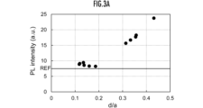
- FIG. 4 is a diagram showing experimental results of dependence of PL detection intensity (vertical axis) on d/a (horizontal axis).
- FIG. 4 is a diagram showing experimental results of the dependence of PL detection intensity on lattice constant a.
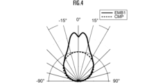
- 4 is a graph showing the light distribution (EMB1, solid line) of the light-emitting diode 10 of the first embodiment in comparison with the light distribution (CMP, broken line) of the LED of the comparative example.
- FIG. 4 is a diagram showing that, in the light-emitting diode 10 of the present embodiment, a laterally propagating low-order mode is narrowed in the photonic crystal layer 21P, and a narrowed-angle light distribution characteristic is obtained.
- FIG. 10 is a diagram showing that in the LED (CMP) of the comparative example, the extraction efficiency of low-order mode light emitted from the light-emitting layer and laterally propagating is low.
- FIG. 5 is a plan view schematically showing the upper surface of a light emitting diode 50 of a second embodiment
- FIG. 6B is a cross-sectional view schematically showing a cross-sectional structure taken along line AA shown in FIG. 6A
- 4 is a flow chart showing a procedure for determining the structure of a light emitting diode 50
- It is a figure which shows the result of a waveguide mode simulation.
- FIG. 4 is a diagram schematically showing a center position AC in the layer thickness direction of the light emitting layer 23A and a light intensity distribution FO when the direction perpendicular to the light emitting layer 23A is the x direction;
- FIG. 4 is a diagram schematically showing a center position AC in the layer thickness direction of the light emitting layer 23A and a light intensity distribution FO when the direction perpendicular to the light emitting layer 23A is the x direction;
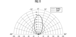
- FIG. 4 is a diagram showing an electric field distribution E y (x) with respect to position in the x direction; 4 is a graph showing difference ⁇ x with respect to layer thickness Ts of spacer layer 23B. 7 is a graph showing the light distribution (EMB2, solid line) of the light-emitting diode 50 of the second embodiment in comparison with the light distribution (CMP, broken line) of the LED of the comparative example.
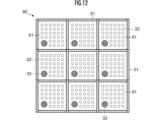
- FIG. 11 is a plan view schematically showing the upper surface (light emitting surface) of a light emitting diode device 60 of a third embodiment;
- FIG. 1A is a plan view schematically showing the top surface of the light emitting diode element 10 of the first embodiment of the present invention
- FIG. 1B schematically shows the cross-sectional structure along the line AA shown in FIG. 1A. It is a sectional view showing.
- a light-emitting diode element (hereinafter simply referred to as a light-emitting diode) 10 includes a moth-eye nanostructure (NPSS: Nano pattern with sapphire substrate) substrate (hereinafter, NPSS substrate) 11 and a semiconductor light-emitting structure provided on the NPSS substrate 11. and a layer (hereinafter referred to as LED structural layer) 20 .
- the LED structure layer 20 has a first semiconductor layer 21 with a photonic crystal layer 21P, an active layer 23 and a second semiconductor layer 25.
- the LED structure layer 20 is made of a nitride-based semiconductor layer (GaN-based semiconductor layer) will be described. good.
- composition, layer thickness, impurities, doping concentration, etc. of each layer of the semiconductor structure layer shown below are merely examples, and can be appropriately selected, modified, etc., according to desired characteristics.
- the photonic crystal layer 21P has fine air holes 22 periodically formed two-dimensionally in a plane parallel to the first semiconductor layer 21.
- the NPSS substrate 11 is a sapphire substrate having a light emitting surface 11S from which light from the LED structure layer 20 is emitted as emitted light LE.
- the NPSS substrate 11 has protrusions with a moth-eye structure on the surface opposite to the light exit surface 11S.
- the NPSS substrate 11 has, on its surface, a protrusion-like structure (moth-eye structure) in which conical protrusions having a period of 200 nm, a height of 150 nm, and a bottom diameter of 120 nm are periodically formed in a grid pattern. ) 11M.
- a protrusion of the moth-eye structure 11M protrudes toward the first semiconductor layer 21 .
- the NPSS substrate 11 has a thickness of 150 ⁇ m, for example.
- the protrusions of the moth-eye structure 11M are not limited to the examples described above. It suffices if the protrusions are periodically formed in a grid pattern. For example, protrusions having a period of 440 nm, a height of 400 nm, and a bottom diameter of 320 nm may be periodically formed in a grid pattern.
- the size and period of the projections of the moth-eye structure 11M can be appropriately set according to the emission wavelength of the LED structure layer 20, the light distribution pattern of the light emitting diode 10, and the like.
- the moth-eye structure 11M allows the light from the LED structure layer 20 to be extracted outside as narrow-angle light.
- An n-GaN layer having a thickness of 5700 nm is provided as the first semiconductor layer 21 on the moth-eye structure 11M of the NPSS substrate 11 .
- Each semiconductor layer on the first semiconductor layer 21 will be described below in the order of lamination.
- the distance between the photonic crystal layer 21P provided in the first semiconductor layer 21 and the top surface of the protrusion of the moth-eye structure 11M is 5740 nm.
- the holes 22 of the photonic crystal layer 21P are arranged with two-dimensional periodicity in a plane parallel to the first semiconductor layer 21 .
- the holes 22 are arranged at square lattice positions, have a columnar shape, and have a lattice constant (period) of 185 nm, a height of 240 nm, and a diameter of 95 nm.
- the embedded layer 21B is made of n-GaN, which is an n-type semiconductor layer, and has a layer thickness of 120 nm.
- the lattice constant of the photonic crystal a
- the emission wavelength ⁇ (in a vacuum)
- ⁇ at this time holds not only for the peak wavelength but also for any wavelength ⁇ w (in vacuum) within the full width at half maximum of the emission spectrum of the active layer.
- the present invention is preferably a light-emitting element that emits non-resonant LED light. By forming only the photonic crystal that satisfies such conditions, the angle of non-resonant light is narrowed.
- a power source (not shown) connected to the light-emitting diode 10 supplies a current value that does not generate resonant light, so that both the narrow-angle light component (with an output angle of 20°) and the wide-angle light component (with an output angle of 20°) It can be a light-emitting element that irradiates non-resonant LED light, as in the case of 100°.
- a light-emitting layer 23A is formed on the first semiconductor layer 21 .
- the light emitting layer 23A is a multiple quantum well structure layer (hereinafter referred to as an MQW layer) having a five-layer structure in which GaN barrier layers and InGaN well layers are alternately laminated.
- a spacer layer 23B is formed on the light emitting layer 23A.
- the spacer layer 23B is made of GaN and has a layer thickness of 6 nm.
- a second semiconductor layer 25 is formed on the spacer layer 23B. More specifically, the second semiconductor layer 25 includes an electron blocking layer 25A and a p-GaN layer 25B, which is a p-type semiconductor layer, formed on the electron blocking layer 25A.
- the electron block layer 25A is made of AlGaN and has a layer thickness of 10 nm, for example.
- the p-GaN layer 25B has a layer thickness of 116 nm, for example.
- a layer composed of the light emitting layer 23A and the spacer layer 23B is referred to as an active layer (core layer) 23.
- the first semiconductor layer 21 and the second semiconductor layer 25 sandwiching the active layer 23 from both sides function as a first clad layer and a second clad layer, respectively.
- the first semiconductor layer (first cladding layer) 21 contains the photonic crystal layer 21P, ie, the holes 22, it has a lower refractive index than the base semiconductor (GaN in this embodiment), and thus has an active
- the effective refractive index is smaller than that of the layer (core layer) 23 .
- the electron blocking layer 25A is made of a semiconductor (AlGaN in this embodiment) having a larger bandgap and a smaller refractive index than the active layer 23 (that is, the spacer layer 23B of the active layer 23).
- the effective refractive index of the layer (second clad layer) 25 is smaller than that of the active layer 23 .
- the first semiconductor layer 21 and the second semiconductor layer 25 have the same function as, for example, the clad of an optical fiber, that is, the function of confining light guided through the active layer (core layer) 23 .
- the first semiconductor layer 21 may be composed of a plurality of semiconductor layers with different compositions.
- the second semiconductor layer 25 may be composed of a plurality of semiconductor layers having different compositions.
- the first semiconductor layer 21 is an n-type semiconductor layer
- the second semiconductor layer 25 is a p-type (conductivity type opposite to that of the first semiconductor layer 21) semiconductor layer.
- Layer 21 and second semiconductor layer 25 may have an i-layer or an undoped layer.
- the electron block layer 25A in the second semiconductor layer 25 may be configured as an undoped layer.
- a p-electrode 31 is provided on the p-GaN layer 25B.
- the p-electrode 31 is formed as a Ni/Au structure (Au is the surface layer) composed of, for example, Ni (nickel) formed on the p-GaN layer 25B and Au (gold) formed on the Ni.
- the p-electrode 31 can use a metal layer that is in ohmic contact with the p-GaN layer 25B.
- a metal layer that is in ohmic contact with the p-GaN layer 25B.
- it is a configuration using an ITO electrode/Ag reflective film having a high reflectance.
- a semiconductor layer (for example, a highly doped layer) that easily makes ohmic contact with the metal layer may be provided on the p-GaN layer 25B.
- an n-electrode 35 is provided on the exposed surface of the first semiconductor layer 21 where the embedded layer 21B is partially exposed by etching.
- the n-electrode 35 is in ohmic contact with the first semiconductor layer 21 .
- the n-electrode 35 has, for example, an Al (aluminum)/Pt (platinum)/Au structure (Au is the surface layer).
- the light-emitting diode 10 is mounted on a substrate or block provided with a wiring circuit with the p-electrode 31 and the n-electrode 35 facing downward.
- the light-emitting diode 10 emits light by energizing between the p-electrode 31 and the n-electrode 35 .
- An example of the fabrication process of the light-emitting diode 10, which is a photonic crystal LED, will be described below.
- an NPSS substrate 11 was prepared by forming a moth-eye structure 11M with a period of 356 nm on a sapphire substrate. Then, an n-GaN layer was grown on the moth-eye structure 11M of the NPSS substrate 11 by MOCVD (metal organic chemical vapor deposition).
- MOCVD metal organic chemical vapor deposition
- a layer of SiO2, SiN, etc. was deposited on the n-GaN layer by a method such as sputtering or plasma CVD. Subsequently, a resist film was formed on the hard mask film, and a square lattice resist pattern with a lattice constant of 185 nm and a hole diameter of 92.5 nm was formed by electron beam lithography.
- the hard mask was dry-etched with CF (fluorocarbon) gas to form a hard mask.
- CF fluorocarbon
- the n-GaN layer was further etched with a chlorine (Cl)-based gas to a depth of 240 nm to form holes arranged in a square lattice.
- n-GaN layer 21P After etching, crystal growth of the n-GaN layer was performed again by the MOCVD apparatus. As a result of this crystal growth, a photonic crystal layer 21P having holes 22 arranged at square lattice positions and a buried layer 21B filling the photonic crystal layer 21P were formed. An n-GaN layer 21A is formed between the photonic crystal layer 21P and the NPSS substrate 11. As shown in FIG.
- a light-emitting layer 23A, a spacer layer 23B, an electron blocking layer (p-cladding layer) 25A, and a p-GaN layer 25B were sequentially grown on the buried layer 21B.
- the NPSS substrate 11 is a sapphire substrate. If it is, the same effect will be exhibited regardless of the material. For example, it may be a semiconductor substrate such as GaN or Si (silicon). In the present invention, materials other than sapphire are also referred to as NPSS for convenience.
- the photonic crystal layer 21P has a function of irradiating narrow-angle light, but the NPSS substrate 11 is required to have a pyramidal periodic structure that can extract narrow-angle light as it is.
- a pyramid-shaped periodic structure that does not diffract the light narrowed by the photonic crystal and suppresses reflection at the interface between the photonic crystal layer 21P and the NPSS substrate 11, or
- the photonic crystal A conical periodic structure that diffracts light whose angle is narrowed from the angle to a predetermined angle or less is obtained.
- wavelength ⁇ vacuum wavelength
- medium refractive index n s medium refractive index
- substrate refractive index n order m
- the wavelength ⁇ is set to 445 nm, and the non-diffracting period is obtained.
- the periodic pattern should have a cone shape to form a refractive index gradient.
- the period of the conical shape is P ⁇ / ns .
- Fresnel reflection is suppressed compared to a flat surface without an uneven structure by being treated as a surface with a refractive index gradient.
- the height of the pattern is at least ⁇ / 2ns (wavelength ⁇ ) or more, more preferably ⁇ / ns (wavelength ⁇ ) or more. In the case of the above example, by satisfying P ⁇ / ns , the expression (3) is also satisfied at the same time.
- m 1 and m 2 are orders.
- m 1 ⁇ 1
- m 2 1.
- equation (4) when ⁇ in ⁇ 20°, the relationship between ⁇ and the wavelength that satisfies -20° ⁇ ⁇ out ⁇ 20° is calculated under the condition that the absolute value of the light is emitted at an angle smaller than 20°. , we obtain the following equation (5).
- the narrow-angle light of 20° or less increased by the action of the photonic crystal can be emitted as narrow-angle light of ⁇ 10° to 20° without widening through the NPSS. can.
- the light incident on the NPSS structure also includes a reflected component, it is reflected by the electrodes and the like formed on the opposing surface, and is incident on the NPSS again. Since the NPSS reflects light at a different angle than the incident angle, part of the light re-entering the NPSS is also extracted as narrow-angle light at the same time, greatly increasing the output of narrow-angle light.
- the arrangement of the dot-like protrusions may be a hexagonal lattice arrangement or a square lattice arrangement.
- the comparative example has the same configuration as the present embodiment except that the sapphire substrate has a flat surface on which the NPSS structure is not formed.
- the light output was 150 mW in the comparative example and 220 mW in the present embodiment, and that the light output was improved by 1.5 times or more as compared with a flat substrate having no concave-convex structure.
- Photonic crystals have the ability to exclude light of a certain frequency from within the crystal, and the frequency range can be freely set, which is called the photonic bandgap.
- the dispersion relation is obtained from the photonic bandgap calculation.
- the dispersion relation of the TE mode (Transverse Electric mode) when the holes are arranged in a square lattice is calculated.
- the diffraction angle is ⁇
- the wavenumber k is 2 ⁇ / ⁇ .
- TE0 which is the lowest order among the plurality of TE modes.
- FIG. 2B is an enlarged view of the maximum value of TE0. As shown in FIG. 2B, matching the normalized frequency to the optical mode edge (white circle in the figure) corresponds to extracting narrow-angle light in the direction of 0°.
- a lattice constant design value of 185 nm is obtained from the normalized frequency of 0.415 at the point (black circle in the figure) that satisfies the intersection of the optical mode (TE0) and the diffraction line. Therefore, the holes 22 are arranged in a square lattice with a hole diameter d of 92.5 nm and a lattice constant a of 185 nm to constitute the photonic crystal layer 21P, and the holes 22 are arranged in a 1 mm square in-plane region. Note that the hole arrangement of the photonic crystal layer 21P is not limited to a square lattice, and can be obtained by appropriately selecting from a triangular lattice, a hexagonal lattice, or the like, and following the same procedure.
- the design value may be determined from the intersection point of the diffraction lines and the theoretical value, but it may also be determined after actually fabricating multiple photonic crystal structures with slightly shifted lattice constants and setting the conditions. .
- the lattice constant a and the diameter of the hole 22 are determined so that the peak value of the intensity is within a desired range.
- An optimal value for d can also be obtained.
- the angle of narrow-angle light by the photonic crystal (the angle at which the intensity peaks) is determined, and the above condition (ii) is satisfied.
- the period of the NPSS projections can also be determined by setting ⁇ in slightly wider than the angle of the peak value (peak value +10°).
- FIG. 3A shows experimental results of the dependence of PL detection intensity (vertical axis) on d/a (horizontal axis).
- FIG. 3B shows experimental results of the dependence of the PL detection intensity (vertical axis) on the lattice constant a (horizontal axis).
- 3A and 3B show the reference level (REF) of the PL intensity.
- the PL intensity increases as d/a increases, and that d/a is preferably 0.3 or more (0.3 ⁇ d/a). have understood.
- the PL intensity has a peak value depending on the lattice constant a. Based on experimental results, a lattice constant of 190 nm (dashed line in FIG. 3B) can be determined to maximize the PL intensity.
- the holes 22 are formed with a period a for extracting narrow-angle light of ⁇ 10°.
- a surrounding low refractive index region n ⁇ 2.4
- the light intensity of the cladding has an evanescent light distribution that decreases exponentially with distance.
- a TE (transverse electric) mode in which the electric field oscillates in the horizontal direction of the waveguide, let us consider the seepage length q of the evanescent light of the mode corresponding to the lowest-order TE0 mode.
- the intensity distribution I(x) of the evanescent light at the light intensity I o and the distance x is given by Equation (6).
- the seepage length q of the evanescent light was estimated to be 60 nm. From the above, it is preferable that the height of the photonic crystal layer 21P is h ⁇ 60 nm.
- the height of the holes 22 is preferably equal to or greater than the seepage length q of the evanescent light in the TE0 mode light from the light emitting layer 23A.
- FIG. 4 is a graph showing the light distribution (EMB1, solid line) of the light-emitting diode 10 of the first embodiment in comparison with the light distribution (CMP, broken line) of the LED of the comparative example.
- the LED (CMP) of the comparative example differs from the light-emitting diode 10 (EMB1) in that it does not have the photonic crystal layer 21P, and has the same configuration as the light-emitting diode 10 in other respects.
- the narrow-angle light component within ⁇ 15° is greatly increased compared to the conventional LED, and the light-emitting diode 10 has narrow-angle light distribution characteristics. It can be seen that a light emitting diode has been realized.
- the angle of the laterally propagating low-order mode (the arrow in the figure) is narrowed by the photonic crystal layer 21P, and the narrow-angle light is maintained by the NPSS substrate 11.
- a narrow-angle light distribution characteristic is obtained.
- the LED (CMP) of the comparative example has the NPSS substrate 11
- the n-GaN layer 91 between the light emitting layer 23A and the NPSS substrate 11 has a photonic crystal structure. This is not provided, and the extraction efficiency of low-order mode light (indicated by arrows in the figure) that is emitted from the light emitting layer and laterally propagates is low.
- FIG. 6A is a plan view schematically showing the top surface of a light-emitting diode 50 according to a second embodiment of the present invention
- FIG. 6B schematically shows a cross-sectional structure along line AA shown in FIG. 6A. It is a sectional view.
- FIG. 7 is a flow chart showing the procedure for determining the structure of the light emitting diode 50. As shown in FIG.
- the LED structure layer 20 has a rectangular parallelepiped shape, and a reflective film 51 is formed to cover all sides of the LED structure layer 20 of the light-emitting diode 50 . is formed.
- the reflective film 51 may be formed so as to cover at least the four side surfaces of the light emitting layer 23A in the LED structure layer 20.
- a surrounding low refractive index region including a photonic crystal portion for example, n ⁇ 2.4
- Equation (8) the electric field distribution E y (x) of light traveling in the z direction (horizontal direction) of the xyz directions is given by Equation (8).
- Equation (9) the eigen equation obtained by converting Maxwell's equation to H(z) and obtaining the continuity condition of H(z) is given by Equation (9).
- the number of modes is 6 (TE0 to TE5)
- the number of modes is 3 (TE0 to TE2)
- the number of modes is 2 (TE0, TE2).
- the lowest-order mode is TE0
- the core layer is formed under the conditions that the number of modes is within 6 (TE0 to TE5) and the optical confinement factor is 90% or more at TE0.
- the optical confinement factor f reaches 97% at TE0 and 90% at TE1.
- the loss increases and the light is attenuated with each iteration of propagation in the waveguide.
- FIG. 9A schematically shows the light intensity distribution FO when the center position (center line: AC) in the layer thickness direction of the light emitting layer 23A and the direction perpendicular to the light emitting layer 23A (the direction of the NPSS substrate 11) is the x direction. is a diagram shown in FIG.
- FIG. 9B is a diagram showing the electric field distribution E y (x) with respect to the position in the x direction.
- the difference ⁇ x between the peak positions of the electric field distribution E y (x) with respect to the central position AC of the light emitting layer 23A is schematically shown.
- the layer thickness is finally determined so as to minimize this difference ⁇ x (FIG. 7, step S13).
- the total thickness of the active layer (core layer) 23 (light-emitting layer 23A+spacer layer 23B) and the buried layer 21B on the photonic crystal 21P is 500 nm. was optimized as an example.
- FIG. 9B shows the light intensity distribution (electric field distribution E y (x)) of TE0 mode light when the layer thickness Ts of the spacer layer 23B is 100 nm, and shows the positional relationship with the center AC of the light emitting layer 23A. ing. It can be seen that the shift ⁇ x of the peak position FC of the electric field distribution E y (x) from the center AC of the light emitting layer 23A is about 40 nm.
- the waveguide mode simulation is performed to extract the conditions under which only a small number of low-order modes propagate in the waveguide (FIG. 7, step S11), and the light intensity distribution simulation (FIG. 7, step S12).
- the center of the light emitting layer 23A With aligning the center of the light emitting layer 23A with the center of the light intensity distribution for the guided light of the low-order mode, especially the TE0 mode light, a light distribution characteristic with high light emission efficiency and a narrow angle is obtained. It is possible to provide a light emitting diode having
- the narrow angle in the photonic crystal portion It is possible to efficiently create the propagating light to be transformed.
- the reflective film 51 provided on the side surface of the LED structure layer 20 will be described below.
- an LED having an emission wavelength ⁇ of 445 nm and an active layer (core layer) 23 including the light emitting layer 23A having a thickness of 1 ⁇ m is assumed.
- the case of the condition having six TE modes will be described as an example.
- the reflection angles when reaching the waveguide end face (side surface) are 84.9° for TE0, 79.9° for TE1, 74.8° for TE2, and 74.8° for TE3, respectively. 69.6°, TE4 at 64.2°, and TE5 at 58.8°.
- the light incident angle ⁇ with respect to the end face is 5.1° for TE0 and 10.1° for TE1.
- TE2 is 15.2°
- TE3 is 20.4°
- TE4 is 25.8°
- TE5 is 31.2°.
- the total reflection angle of light from the semiconductor layer to the air interface is 23.6°, and under the condition of the incident angle equal to or greater than the total reflection angle, the light is reflected even if there is no reflective periodic structure. Therefore, among the six modes, it is important that the reflective film 51 reflects low-order mode light up to TE3.
- the reflective film 51 can be realized by forming a dielectric multilayer film such as TiO 2 /SiO 2 (titanium oxide film/silicon oxide film).
- a dielectric multilayer film such as TiO 2 /SiO 2 (titanium oxide film/silicon oxide film).
- the film thickness condition of the low refractive material can be determined in a similar manner.
- FIG. 11 is a graph showing the light distribution (EMB2, solid line) of the light-emitting diode 50 of the second embodiment in comparison with the light distribution (CMP, broken line) of the LED of the comparative example.
- the LED (CMP) of the comparative example differs from the light-emitting diode 50 (EMB2) in that it does not have the photonic crystal layer 21P and the reflective film 51, and has the same configuration as the light-emitting diode 50 in other respects.
- FIG. 12 is a plan view schematically showing the upper surface (light emitting surface) of a light emitting diode device 60 according to the third embodiment of the invention.
- the light-emitting diode device 60 has the same structure as the light-emitting diode 50 of the second embodiment, but is configured by arranging a plurality of small-sized light-emitting diodes 61 adjacently in a matrix.
- each of the plurality of light emitting diodes 61 has a small size for sufficient current spreading.
- each of the light emitting diodes 61 has uniform and highly efficient light emission characteristics. Further, by making the overall size of the light-emitting diode device 60 approximately the same as that of the single light-emitting diode 50 of the second embodiment, for example, the light-emitting diode device has narrow-angle light distribution, uniform, and highly efficient light emission characteristics. can be realized.
- the present invention is not limited to this, and can also be applied to a light-emitting diode having a photonic crystal layer with a multi-lattice structure.
- photonic crystal light emitting diodes made of nitride semiconductors were described, but the present invention is not limited to this, and can be applied to photonic crystal light emitting diodes made of semiconductors of other crystal systems.
Landscapes
- Led Devices (AREA)
Priority Applications (4)
| Application Number | Priority Date | Filing Date | Title |
|---|---|---|---|
| KR1020247016456A KR20240101933A (ko) | 2021-11-24 | 2022-11-01 | 발광다이오드 소자 |
| EP22898358.1A EP4415061B1 (en) | 2021-11-24 | 2022-11-01 | Light-emitting diode element |
| CN202280076604.7A CN118266092A (zh) | 2021-11-24 | 2022-11-01 | 发光二极管元件 |
| US18/711,620 US20250031489A1 (en) | 2021-11-24 | 2022-11-01 | Light-emitting diode element |
Applications Claiming Priority (2)
| Application Number | Priority Date | Filing Date | Title |
|---|---|---|---|
| JP2021189929A JP7738851B2 (ja) | 2021-11-24 | 2021-11-24 | 発光ダイオード素子 |
| JP2021-189929 | 2021-11-24 |
Publications (1)
| Publication Number | Publication Date |
|---|---|
| WO2023095573A1 true WO2023095573A1 (ja) | 2023-06-01 |
Family
ID=86539405
Family Applications (1)
| Application Number | Title | Priority Date | Filing Date |
|---|---|---|---|
| PCT/JP2022/040884 Ceased WO2023095573A1 (ja) | 2021-11-24 | 2022-11-01 | 発光ダイオード素子 |
Country Status (6)
| Country | Link |
|---|---|
| US (1) | US20250031489A1 (https=) |
| EP (1) | EP4415061B1 (https=) |
| JP (1) | JP7738851B2 (https=) |
| KR (1) | KR20240101933A (https=) |
| CN (1) | CN118266092A (https=) |
| WO (1) | WO2023095573A1 (https=) |
Families Citing this family (1)
| Publication number | Priority date | Publication date | Assignee | Title |
|---|---|---|---|---|
| WO2025018206A1 (ja) * | 2023-07-20 | 2025-01-23 | スタンレー電気株式会社 | 半導体発光素子及び半導体発光素子用基板 |
Citations (5)
| Publication number | Priority date | Publication date | Assignee | Title |
|---|---|---|---|---|
| JP2007329468A (ja) * | 2006-05-10 | 2007-12-20 | Kumamoto Univ | 発光素子およびその製造方法 |
| JP5553292B1 (ja) * | 2013-12-03 | 2014-07-16 | エルシード株式会社 | Led素子 |
| JP2015109477A (ja) | 2015-02-27 | 2015-06-11 | エルシード株式会社 | Led素子 |
| CN108511572A (zh) * | 2017-02-23 | 2018-09-07 | 海迪科(南通)光电科技有限公司 | 一种具有光子晶体结构的发光二极管 |
| JP2020107778A (ja) * | 2018-12-28 | 2020-07-09 | 丸文株式会社 | 深紫外led装置及びその製造方法 |
Family Cites Families (9)
| Publication number | Priority date | Publication date | Assignee | Title |
|---|---|---|---|---|
| JP5597933B2 (ja) * | 2009-05-01 | 2014-10-01 | 住友電気工業株式会社 | Iii族窒化物半導体層貼り合わせ基板およびその製造方法 |
| ES2663320T3 (es) * | 2009-09-07 | 2018-04-12 | El-Seed Corporation | Elemento emisor de luz semiconductor |
| JP5435523B1 (ja) * | 2012-10-12 | 2014-03-05 | エルシード株式会社 | 半導体発光素子及びその製造方法 |
| JPWO2014115830A1 (ja) * | 2013-01-28 | 2017-01-26 | エルシード株式会社 | 半導体発光素子の製造方法 |
| JP5643920B1 (ja) * | 2013-04-16 | 2014-12-17 | エルシード株式会社 | Led素子及びその製造方法 |
| US10168450B2 (en) * | 2013-12-27 | 2019-01-01 | Sunasic Technologies, Inc. | Silicon wafer having colored top side |
| JP2015146302A (ja) * | 2014-02-04 | 2015-08-13 | 株式会社リコー | 直管形ledランプ及び照明装置 |
| WO2017038961A1 (ja) * | 2015-09-03 | 2017-03-09 | 丸文株式会社 | 深紫外led及びその製造方法 |
| US11296262B2 (en) * | 2017-12-21 | 2022-04-05 | Lumileds Llc | Monolithic segmented LED array architecture with reduced area phosphor emission surface |
-
2021
- 2021-11-24 JP JP2021189929A patent/JP7738851B2/ja active Active
-
2022
- 2022-11-01 EP EP22898358.1A patent/EP4415061B1/en active Active
- 2022-11-01 KR KR1020247016456A patent/KR20240101933A/ko active Pending
- 2022-11-01 US US18/711,620 patent/US20250031489A1/en active Pending
- 2022-11-01 CN CN202280076604.7A patent/CN118266092A/zh active Pending
- 2022-11-01 WO PCT/JP2022/040884 patent/WO2023095573A1/ja not_active Ceased
Patent Citations (5)
| Publication number | Priority date | Publication date | Assignee | Title |
|---|---|---|---|---|
| JP2007329468A (ja) * | 2006-05-10 | 2007-12-20 | Kumamoto Univ | 発光素子およびその製造方法 |
| JP5553292B1 (ja) * | 2013-12-03 | 2014-07-16 | エルシード株式会社 | Led素子 |
| JP2015109477A (ja) | 2015-02-27 | 2015-06-11 | エルシード株式会社 | Led素子 |
| CN108511572A (zh) * | 2017-02-23 | 2018-09-07 | 海迪科(南通)光电科技有限公司 | 一种具有光子晶体结构的发光二极管 |
| JP2020107778A (ja) * | 2018-12-28 | 2020-07-09 | 丸文株式会社 | 深紫外led装置及びその製造方法 |
Non-Patent Citations (2)
| Title |
|---|
| KAZUAKI SAKODA: "Introduction to Photonic Crystal", MORIKITA PUBLISHING CO., LTD. |
| See also references of EP4415061A4 |
Also Published As
| Publication number | Publication date |
|---|---|
| EP4415061B1 (en) | 2026-05-06 |
| CN118266092A (zh) | 2024-06-28 |
| JP2023076901A (ja) | 2023-06-05 |
| EP4415061A1 (en) | 2024-08-14 |
| EP4415061A4 (en) | 2025-03-12 |
| KR20240101933A (ko) | 2024-07-02 |
| US20250031489A1 (en) | 2025-01-23 |
| JP7738851B2 (ja) | 2025-09-16 |
Similar Documents
| Publication | Publication Date | Title |
|---|---|---|
| US8004003B2 (en) | Light emitting device having light extraction structure | |
| US8410503B2 (en) | Light emitting devices | |
| JP5553292B1 (ja) | Led素子 | |
| US20130126902A1 (en) | Semiconductor light emitting element | |
| US8378567B2 (en) | Light-polarizing structure | |
| US20120112218A1 (en) | Light Emitting Diode with Polarized Light Emission | |
| JP7316610B2 (ja) | 深紫外led及びその製造方法 | |
| JP2008283037A (ja) | 発光素子 | |
| JP7738851B2 (ja) | 発光ダイオード素子 | |
| Shin et al. | Effects of nanometer-scale photonic crystal structures on the light extraction from GaN light-emitting diodes | |
| JP5071087B2 (ja) | 半導体発光素子 | |
| JP7784084B2 (ja) | 発光装置 | |
| JP2008159894A (ja) | 発光素子及び照明装置 | |
| KR100987358B1 (ko) | 포토닉 크리스탈 구조가 형성된 발광 소자 및 그 제조 방법 | |
| JP5740031B2 (ja) | Led素子 | |
| JP2015109477A (ja) | Led素子 |
Legal Events
| Date | Code | Title | Description |
|---|---|---|---|
| 121 | Ep: the epo has been informed by wipo that ep was designated in this application |
Ref document number: 22898358 Country of ref document: EP Kind code of ref document: A1 |
|
| WWE | Wipo information: entry into national phase |
Ref document number: 22898358.1 Country of ref document: EP Ref document number: 2022898358 Country of ref document: EP |
|
| WWE | Wipo information: entry into national phase |
Ref document number: 202280076604.7 Country of ref document: CN |
|
| ENP | Entry into the national phase |
Ref document number: 2022898358 Country of ref document: EP Effective date: 20240510 |
|
| WWE | Wipo information: entry into national phase |
Ref document number: 18711620 Country of ref document: US |
|
| NENP | Non-entry into the national phase |
Ref country code: DE |