WO2023090165A1 - 半導体モジュール - Google Patents
半導体モジュール Download PDFInfo
- Publication number
- WO2023090165A1 WO2023090165A1 PCT/JP2022/041140 JP2022041140W WO2023090165A1 WO 2023090165 A1 WO2023090165 A1 WO 2023090165A1 JP 2022041140 W JP2022041140 W JP 2022041140W WO 2023090165 A1 WO2023090165 A1 WO 2023090165A1
- Authority
- WO
- WIPO (PCT)
- Prior art keywords
- wiring member
- signal
- wiring
- semiconductor
- metal layer
- Prior art date
- Legal status (The legal status is an assumption and is not a legal conclusion. Google has not performed a legal analysis and makes no representation as to the accuracy of the status listed.)
- Ceased
Links
Images


Classifications
-
- H—ELECTRICITY
- H10—SEMICONDUCTOR DEVICES; ELECTRIC SOLID-STATE DEVICES NOT OTHERWISE PROVIDED FOR
- H10W—GENERIC PACKAGES, INTERCONNECTIONS, CONNECTORS OR OTHER CONSTRUCTIONAL DETAILS OF DEVICES COVERED BY CLASS H10
- H10W70/00—Package substrates; Interposers; Redistribution layers [RDL]
- H10W70/40—Leadframes
- H10W70/464—Additional interconnections in combination with leadframes
- H10W70/467—Multilayered additional interconnections
-
- H—ELECTRICITY
- H02—GENERATION; CONVERSION OR DISTRIBUTION OF ELECTRIC POWER
- H02M—APPARATUS FOR CONVERSION BETWEEN AC AND AC, BETWEEN AC AND DC, OR BETWEEN DC AND DC, AND FOR USE WITH MAINS OR SIMILAR POWER SUPPLY SYSTEMS; CONVERSION OF DC OR AC INPUT POWER INTO SURGE OUTPUT POWER; CONTROL OR REGULATION THEREOF
- H02M7/00—Conversion of AC power input into DC power output; Conversion of DC power input into AC power output
- H02M7/42—Conversion of DC power input into AC power output without possibility of reversal
- H02M7/44—Conversion of DC power input into AC power output without possibility of reversal by static converters
- H02M7/48—Conversion of DC power input into AC power output without possibility of reversal by static converters using discharge tubes with control electrode or semiconductor devices with control electrode
-
- H—ELECTRICITY
- H10—SEMICONDUCTOR DEVICES; ELECTRIC SOLID-STATE DEVICES NOT OTHERWISE PROVIDED FOR
- H10W—GENERIC PACKAGES, INTERCONNECTIONS, CONNECTORS OR OTHER CONSTRUCTIONAL DETAILS OF DEVICES COVERED BY CLASS H10
- H10W40/00—Arrangements for thermal protection or thermal control
- H10W40/10—Arrangements for heating
-
- H—ELECTRICITY
- H10—SEMICONDUCTOR DEVICES; ELECTRIC SOLID-STATE DEVICES NOT OTHERWISE PROVIDED FOR
- H10W—GENERIC PACKAGES, INTERCONNECTIONS, CONNECTORS OR OTHER CONSTRUCTIONAL DETAILS OF DEVICES COVERED BY CLASS H10
- H10W40/00—Arrangements for thermal protection or thermal control
- H10W40/20—Arrangements for cooling
- H10W40/25—Arrangements for cooling characterised by their materials
- H10W40/255—Arrangements for cooling characterised by their materials having a laminate or multilayered structure, e.g. direct bond copper [DBC] ceramic substrates
-
- H—ELECTRICITY
- H10—SEMICONDUCTOR DEVICES; ELECTRIC SOLID-STATE DEVICES NOT OTHERWISE PROVIDED FOR
- H10W—GENERIC PACKAGES, INTERCONNECTIONS, CONNECTORS OR OTHER CONSTRUCTIONAL DETAILS OF DEVICES COVERED BY CLASS H10
- H10W40/00—Arrangements for thermal protection or thermal control
- H10W40/70—Fillings or auxiliary members in containers or in encapsulations for thermal protection or control
- H10W40/77—Auxiliary members characterised by their shape
- H10W40/778—Auxiliary members characterised by their shape in encapsulations
-
- H—ELECTRICITY
- H10—SEMICONDUCTOR DEVICES; ELECTRIC SOLID-STATE DEVICES NOT OTHERWISE PROVIDED FOR
- H10W—GENERIC PACKAGES, INTERCONNECTIONS, CONNECTORS OR OTHER CONSTRUCTIONAL DETAILS OF DEVICES COVERED BY CLASS H10
- H10W70/00—Package substrates; Interposers; Redistribution layers [RDL]
- H10W70/40—Leadframes
- H10W70/464—Additional interconnections in combination with leadframes
- H10W70/466—Tape carriers or flat leads
-
- H—ELECTRICITY
- H10—SEMICONDUCTOR DEVICES; ELECTRIC SOLID-STATE DEVICES NOT OTHERWISE PROVIDED FOR
- H10W—GENERIC PACKAGES, INTERCONNECTIONS, CONNECTORS OR OTHER CONSTRUCTIONAL DETAILS OF DEVICES COVERED BY CLASS H10
- H10W70/00—Package substrates; Interposers; Redistribution layers [RDL]
- H10W70/40—Leadframes
- H10W70/464—Additional interconnections in combination with leadframes
- H10W70/468—Circuit boards
-
- H—ELECTRICITY
- H10—SEMICONDUCTOR DEVICES; ELECTRIC SOLID-STATE DEVICES NOT OTHERWISE PROVIDED FOR
- H10W—GENERIC PACKAGES, INTERCONNECTIONS, CONNECTORS OR OTHER CONSTRUCTIONAL DETAILS OF DEVICES COVERED BY CLASS H10
- H10W70/00—Package substrates; Interposers; Redistribution layers [RDL]
- H10W70/40—Leadframes
- H10W70/481—Leadframes for devices being provided for in groups H10D8/00 - H10D48/00
-
- H—ELECTRICITY
- H10—SEMICONDUCTOR DEVICES; ELECTRIC SOLID-STATE DEVICES NOT OTHERWISE PROVIDED FOR
- H10W—GENERIC PACKAGES, INTERCONNECTIONS, CONNECTORS OR OTHER CONSTRUCTIONAL DETAILS OF DEVICES COVERED BY CLASS H10
- H10W72/00—Interconnections or connectors in packages
- H10W72/30—Die-attach connectors
-
- H—ELECTRICITY
- H10—SEMICONDUCTOR DEVICES; ELECTRIC SOLID-STATE DEVICES NOT OTHERWISE PROVIDED FOR
- H10W—GENERIC PACKAGES, INTERCONNECTIONS, CONNECTORS OR OTHER CONSTRUCTIONAL DETAILS OF DEVICES COVERED BY CLASS H10
- H10W74/00—Encapsulations, e.g. protective coatings
- H10W74/10—Encapsulations, e.g. protective coatings characterised by their shape or disposition
- H10W74/111—Encapsulations, e.g. protective coatings characterised by their shape or disposition the semiconductor body being completely enclosed
-
- H—ELECTRICITY
- H10—SEMICONDUCTOR DEVICES; ELECTRIC SOLID-STATE DEVICES NOT OTHERWISE PROVIDED FOR
- H10W—GENERIC PACKAGES, INTERCONNECTIONS, CONNECTORS OR OTHER CONSTRUCTIONAL DETAILS OF DEVICES COVERED BY CLASS H10
- H10W74/00—Encapsulations, e.g. protective coatings
- H10W74/40—Encapsulations, e.g. protective coatings characterised by their materials
-
- H—ELECTRICITY
- H10—SEMICONDUCTOR DEVICES; ELECTRIC SOLID-STATE DEVICES NOT OTHERWISE PROVIDED FOR
- H10W—GENERIC PACKAGES, INTERCONNECTIONS, CONNECTORS OR OTHER CONSTRUCTIONAL DETAILS OF DEVICES COVERED BY CLASS H10
- H10W90/00—Package configurations
-
- H—ELECTRICITY
- H10—SEMICONDUCTOR DEVICES; ELECTRIC SOLID-STATE DEVICES NOT OTHERWISE PROVIDED FOR
- H10W—GENERIC PACKAGES, INTERCONNECTIONS, CONNECTORS OR OTHER CONSTRUCTIONAL DETAILS OF DEVICES COVERED BY CLASS H10
- H10W90/00—Package configurations
- H10W90/701—Package configurations characterised by the relative positions of pads or connectors relative to package parts
- H10W90/731—Package configurations characterised by the relative positions of pads or connectors relative to package parts of die-attach connectors
- H10W90/736—Package configurations characterised by the relative positions of pads or connectors relative to package parts of die-attach connectors between a chip and a stacked lead frame, conducting package substrate or heat sink
Definitions
- the disclosure in this specification relates to a semiconductor module.
- Patent Document 1 discloses a semiconductor module containing semiconductor elements including switching elements.
- This semiconductor module includes a wiring sheet.
- the wiring sheet is formed of a flexible printed circuit board.
- the wiring sheet of Patent Literature 1 includes a land portion for soldering connection between an electrode and a terminal as a power path of a switching element. Furthermore, the wiring sheet of Patent Document 1 includes control wiring connected to control electrodes of switching elements.
- One disclosed object is to provide a semiconductor module that reliably provides electrical isolation between power paths and signal paths.
- the semiconductor module disclosed herein includes a semiconductor element having a signal pad for a signal path and a power pad for a power path for a power greater than the power of the signal pad, and a semiconductor element thermally bonded to the semiconductor element.
- a wiring member having a second joint portion.
- the disclosed semiconductor module accommodates a semiconductor element inside a resin member. Furthermore, the semiconductor module includes metal signal terminals arranged so as to be exposed from the resin member. A signal pad of the semiconductor element and a signal terminal are connected by a wiring member inside the resin member.
- the wiring member is housed in the resin member.
- the wiring member is a member that is more flexible than the signal terminal.
- the wiring member includes an electrically insulating resin layer and a metal layer supported by the resin layer.
- the wiring member has a first junction where the metal layer is connected to the signal pad and a second junction where the metal layer is connected to the signal terminal.
- a semiconductor module provides high connection workability by providing a signal terminal. Moreover, even among the resin members, the workability of connecting the signal paths can be improved by the wiring members.
- a wiring member having an electrically insulating resin layer contributes to electrical insulation between a power path and a signal path. As a result, a semiconductor module is provided that ensures electrical insulation between the power path and the signal path.
- FIG. 1 is a block diagram of an electric system according to a first embodiment;
- FIG. 1 is an external perspective view of a semiconductor module;
- FIG. 1 is a schematic cross-sectional view of a semiconductor module;
- FIG. 4 is a partial cross-sectional view taken along line IV-IV of FIG. 3;
- FIG. It is a perspective view of a semiconductor module of a second embodiment.
- FIG. 11 is a partial cross-sectional view of a semiconductor module according to a third embodiment; It is a perspective view of the semiconductor module of 4th Embodiment. It is a perspective view of the semiconductor module of 5th Embodiment.
- FIG. 11 is a cross-sectional view of a semiconductor module according to a sixth embodiment;
- FIG. 1 is an external perspective view of a semiconductor module
- FIG. 1 is a schematic cross-sectional view of a semiconductor module
- FIG. 4 is a partial cross-sectional view taken along line IV-IV of FIG. 3
- FIG. It is a
- FIG. 11 is a cross-sectional view of a semiconductor module according to a seventh embodiment
- FIG. 21 is a plan view of a wiring member according to an eighth embodiment
- FIG. 21 is a plan view of a wiring member according to a ninth embodiment
- FIG. 20 is a plan view of a wiring member according to a tenth embodiment
- FIG. 21 is a cross-sectional view of a semiconductor module according to an eleventh embodiment
- FIG. 21 is a cross-sectional view of a semiconductor module according to a twelfth embodiment
- 1 is an exploded perspective view showing a semiconductor module
- FIG. FIG. 21 is a cross-sectional view of a semiconductor module according to a thirteenth embodiment
- FIG. 21 is an enlarged cross-sectional view of a semiconductor module according to a fourteenth embodiment;
- FIG. 21 is a cross-sectional view of a semiconductor module according to a fifteenth embodiment;
- FIG. 20 is a cross-sectional view in a bonding step of the sixteenth embodiment; It is a top view which shows a wiring member.
- FIG. 22 is a cross-sectional view in a bonding step of the seventeenth embodiment;
- FIG. 20 is a cross-sectional view in a bonding step of the eighteenth embodiment;
- FIG. 20 is a cross-sectional view of a semiconductor module according to a nineteenth embodiment;
- FIG. 20 is a cross-sectional view of a semiconductor module according to a twentieth embodiment;
- FIG. 21 is a plan view of a semiconductor module according to a twenty-first embodiment
- FIG. 20 is a plan view of a wiring member according to a twenty-second embodiment
- FIG. 21 is a plan view of a wiring member according to a twenty-third embodiment
- FIG. 24 is a perspective view of a wiring member according to a twenty-fourth embodiment
- FIG. 20 is a cross-sectional view of a semiconductor module according to a twenty-fifth embodiment
- 1 is a partial cross-sectional view of a semiconductor module
- FIG. FIG. 26 is a cross-sectional view of a semiconductor module according to a twenty-sixth embodiment
- 1 is a cross-sectional view of a semiconductor module;
- FIG. 22 is a cross-sectional view of a semiconductor module according to a twenty-seventh embodiment
- FIG. 20 is a cross-sectional view of a semiconductor module according to a twenty-eighth embodiment
- FIG. 20 is a cross-sectional view of a semiconductor module according to a twenty-ninth embodiment
- FIG. 21 is a cross-sectional view of a semiconductor module according to a thirtieth embodiment
- FIG. 20 is a cross-sectional view of a semiconductor module according to a thirty-first embodiment
- an electric system 1 includes a power supply device 2 , a rotating electric machine (RM) 3 and a power conversion circuit 4 .
- the power supply device 2 is a chargeable/dischargeable DC power supply.
- Power supply 2 may be provided by a DC power supply including a lithium ion battery, a fuel cell system, or a solar cell system.
- the power supply device 2 is provided by a power generation system that generates power using a power source such as an internal combustion engine.
- the rotating electric machine 3 is provided by an electric motor or a motor-generator.
- the rotating electrical machine 3 is a multiphase AC rotating electrical machine. In the illustrated example, the rotating electrical machine 3 is a three-phase rotating electrical machine.
- the rotating electric machine 3 is used as a power source for a moving body or a power source for machines such as generators and water pumps.
- moving bodies include vehicles, aircraft, ships, amusement machines for riding, and simulation machines for vehicles.
- the power conversion circuit 4 is electrically connected to the power supply device 2 and the rotating electric machine 3 .
- the power conversion circuit 4 converts at least one element of electric power between the power supply device 2 and the rotating electric machine 3 .
- Elements of power include direction of current, cross current, voltage, current, phase, and the like.
- the power conversion circuit 4 can operate in a powering direction in which power is supplied from the power supply device 2 to the rotating electrical machine 3 and/or in a regeneration direction in which power is charged from the rotating electrical machine 3 to the power supply device 2 .
- power conversion circuit 4 provides at least bi-directional voltage conversion and bi-directional AC/DC conversion.
- the power conversion circuit 4 includes a converter circuit 5, a smoothing capacitor 6, an inverter circuit 7, and a control device 8. Power conversion circuit 4 may further comprise inductive and/or capacitive elements that provide a filter circuit.
- Converter circuit 5 is electrically arranged between power supply device 2 and rotating electric machine 3 .
- Converter circuit 5 provides bi-directional voltage conversion.
- the converter circuit 5 may step up or step down the voltage output by the power supply device 2 and output it to the outside.
- Converter circuit 5 steps up or steps down a voltage supplied from the outside and supplies it to power supply device 2 .
- the inverter circuit 7 is electrically arranged between the power supply device 2 and the rotating electric machine 3 .
- Inverter circuit 7 is electrically arranged between converter circuit 5 and rotating electric machine 3 .
- the inverter circuit 7 provides bi-directional DC/AC conversion.
- the inverter circuit 7 provides conversion from direct current to alternating current when power is supplied from the power supply device 2 to the rotating electric machine 3 .
- the inverter circuit 7 provides conversion from alternating current to direct current when power is supplied from the rotating electric machine to the power supply device 23 .
- Smoothing capacitor 6 is arranged between converter circuit 5 and inverter circuit 7 . Smoothing capacitor 6 provides part of a filter circuit that smoothes the DC power.
- the inverter circuit 7 includes a plurality of switching elements 10 (SW elements 10), a plurality of power lines 50, and a plurality of signal lines 60.
- the plurality of SW elements 10 includes, for example, SW element 11 and SW element 12 for U phase, SW element 13 and SW element 14 for V phase, and SW element 15 and SW element 16 for W phase.
- a plurality of SW elements 10 constitute a polyphase bridge circuit together with the power line 50 .
- the polyphase bridge circuit comprises a plurality of switching arms 18 corresponding in number to the phases.
- the U-phase switching arm includes SW element 11 that provides an upper arm and SW element 12 that provides a lower arm.
- the V-phase switching arm includes SW element 13 that provides an upper arm and SW element 14 that provides a lower arm.
- the W-phase switching arm includes SW element 15 that provides an upper arm and SW element 16 that provides a lower arm.
- the plurality of power lines 50 includes positive lines 52 and negative lines 54 .
- the positive line 52 and the negative line 54 are also called a pair of DC buses.
- power line 50 includes connection line 56 and phase line 58 .
- a connection line 56 connects the SW element that provides the upper arm and the SW element that provides the lower arm.
- the phase line 58 connects the connection line 56 and one phase winding of the rotating electric machine 3 . Therefore, the inverter circuit 7 has a plurality of switching arms 18 arranged between a pair of DC buses.
- the plurality of signal lines 60 are electrically connected to each of the plurality of SW elements 10 .
- the signal line 60 may include a drive signal line for switching the SW element 10 and a plurality of detection signal lines for current value, temperature, and the like.
- the converter circuit 5 may also have a switching arm.
- the converter circuit 5 is configured as a chopper circuit including an inductance element.
- the plurality of SW elements 10 have the same or similar configurations.
- One SW element 10 includes a semiconductor element 30 .
- the semiconductor element 30 is a semiconductor made of Si, SiC, or the like, available now or in the future.
- Semiconductor element 30 includes a transistor element 31 and a diode element 32 .
- the transistor element 31 is an IGBT element (Insulated-Gate Bipolar Transistor), a MOS-FET element (Metal-Oxide-Semiconductor Field-Effect Transistor), etc., which is available now or in the future and can be switched in response to a control signal.
- Diode element 32 is a reverse-connected diode.
- a single SW element 10 may comprise a single transistor element or multiple transistor elements connected in series and/or in parallel.
- a single SW element 10 is also called a single semiconductor module 10 or a semiconductor package.
- the semiconductor module 10 is provided by sealing at least one SW element 10 with a resin member 20 which will be described later.
- the semiconductor module 10 may be provided by sealing one switching arm 18 with a resin member 20 .
- the semiconductor module 10 has a plurality of signal terminals exposed to the outside, a pair of power terminals exposed to the outside, and one power terminal providing the phase line 58 .
- one semiconductor module 10 may accommodate multiple switching arms 18 .
- the control device 8 is configured by an electrical circuit. Control device 8 controls converter circuit 5 and inverter circuit 7 . Control device 8 is electrically connected to converter circuit 5 and inverter circuit 7 . The control device 8 and the inverter circuit 7 are connected by a plurality of signal lines 60 . The control device 8 generates and outputs a control signal for controlling at least the inverter circuit 7 .
- the control device 8 in this specification may also be called an electronic control unit (ECU: Electronic Control Unit).
- ECU Electronic Control Unit
- the control device 8 or control system is provided by (a) an algorithm as a plurality of logics called if-then-else format, or (b) a trained model tuned by machine learning, such as an algorithm as a neural network. .
- the control device 8 is provided by a control system including at least one computer.
- a control system may include multiple computers linked by data communication devices.
- a computer includes at least one processor that is hardware (hardware processor).
- a hardware processor may be provided by (i), (ii), or (iii) below.
- the hardware processor may be at least one processor core 8a (CPU) executing programs stored in at least one memory 8b (MMR).
- the computer is provided by at least one memory and at least one processor core.
- the processor core is called CPU: Central Processing Unit, GPU: Graphics Processing Unit, RISC-CPU, or the like.
- Memory is also called a storage medium.
- a memory is a non-transitory and tangible storage medium that non-temporarily stores "programs and/or data" readable by a processor.
- a storage medium is provided by a semiconductor memory, a magnetic disk, an optical disk, or the like.
- the program may be distributed alone or as a storage medium storing the program.
- the hardware processor may be a hardware logic circuit;
- the computer is provided by digital circuits containing a large number of programmed logic units (gate circuits).
- a digital circuit is a logic circuit array, for example, ASIC: Application-Specific Integrated Circuit, FPGA: Field Programmable Gate Array, SoC: System a Chip, PGA: Programmable Gate Array, CPLD: Complex Pro It is also called a grammable logic device.
- a digital circuit may include a memory that stores programs and/or data.
- Computers may be provided by analog circuits. Computers may be provided by a combination of digital and analog circuits.
- the hardware processor may be a combination of (i) above and (ii) above. (i) and (ii) are located on different chips or on a common chip. In these cases, part (ii) is also called an accelerator.
- control device signal source, and controlled object provide various elements. At least some of those elements may be referred to as blocks, modules, or sections. Moreover, the elements included in the control system are called functional means only if they are intentional.
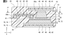
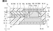
- the semiconductor module 10 will be described in detail with reference to several drawings.
- dimensions such as thickness, width, height, and length of multiple members help understanding of the relative arrangement of multiple members and their positional relationship with each other.
- the thickness in the X direction of the first joint member 71 which will be described later, can be set to about 0.2 millimeters.
- the dimensions of each part are to be understood as having numerical ranges that can be understood as obvious to those of ordinary skill in the present and future semiconductor arts.
- three axial directions are illustrated. The X direction is called the thickness direction, the Y direction is called the width direction, and the Z direction is called the height direction. These names do not reflect the attitude of the semiconductor module 10 in use. These designations should be understood as a matter of convenience.
- the semiconductor module 10 has a flat plate-like outer shape.
- the outer shape is mainly defined by the resin member 20 .
- the resin member 20 is a member obtained by molding a resin material in a molten state into a desired shape using a mold and then hardening it again.
- a non-limiting example of the resin member 20 is epoxy resin.
- the semiconductor module 10 seals the semiconductor element 30 with the resin member 20 .
- the semiconductor element 30 is a semiconductor chip.
- the semiconductor element 30 is a plate-like member.
- the semiconductor module 10 has at least a pair of power terminals 51 exposed to the outside of the resin member 20 .
- the pair of power terminals 51 includes a positive P terminal and a negative N terminal.
- the semiconductor module 10 has a plurality of signal terminals 61 exposed outside the resin member 20 .
- the semiconductor module 10 may have power terminals as input/output terminals of the switching arm.
- the power terminal 51 and the signal terminal 61 can be clearly distinguished by the difference in the power flowing through them.
- the electric power terminal 51 allows the electric power of the rotary electric machine 3 as a controlled object to flow.
- the signal terminal 61 is the control signal for the semiconductor element 30 and the transistor element 31 or the signal level power for the controller 8 .
- the power terminals 51 and the signal terminals 61 are partly embedded inside the resin member 20 and the rest are exposed outside the resin member 20 .
- the power terminal 51 is provided by, for example, a plate material made of metal such as copper or iron.
- the signal terminal 61 is provided by, for example, a plate material made of metal such as copper or iron.
- the power terminals 51 and the signal terminals 61 are provided by metal plates called lead frames.
- the power terminals 51 and the signal terminals 61 extend from any one of the four side surfaces of the outer periphery of the semiconductor module 10 when viewed as a plate.
- the power terminal 51 and the signal terminal 61 have hardness enough to maintain their shape in a room temperature environment.
- the semiconductor module 10 has a heat dissipation member 40 exposed to the outside of the resin member 20 .
- the heat dissipation member 40 is thermally coupled with the semiconductor element 30 .
- the semiconductor module 10 is air-cooled or liquid-cooled.
- the semiconductor module 10 has at least one heat radiating member 40 for radiating heat from the semiconductor element 30 .
- the semiconductor module 10 may be arranged with the exposed surface of the heat radiating member 40 in contact with the coolant pipe. In this case, the semiconductor module 10 indirectly radiates heat from the heat radiating member 40 to the coolant pipe.
- the semiconductor module 10 may be placed in a coolant passageway. In this case, the semiconductor module 10 directly radiates heat to the cooling liquid from the contact surface (including the heat dissipation member 40) with the cooling liquid.
- the heat dissipation member 40 has two heat dissipation members 41 and 42 exposed on both sides of the semiconductor module 10 .
- the heat dissipation member 41 may be called a first heat dissipation member.
- the heat dissipation member 42 may be called a second heat dissipation member.
- the semiconductor module 10 is called a double-sided heat dissipation package.
- the exposed surface of the first heat radiating member 41 is in contact with one cooling liquid pipe between the two cooling liquid pipes, and the exposed surface of the second heat radiating member 42 is in contact with another cooling liquid pipe. It may be placed with
- the semiconductor module 10 indirectly radiates heat from one plate-like surface of the semiconductor element 30 to the coolant pipe through the first heat radiation member 41 .
- the semiconductor module 10 indirectly dissipates heat from the other plate-like surface of the semiconductor element 30 to the coolant pipe through the second heat dissipating member 42 .
- the semiconductor module 10 may be placed in a coolant passageway. In this case, the semiconductor module 10 directly radiates heat to the cooling liquid from the contact surface (including the two heat dissipation members 41 and 42) with the cooling liquid.
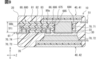
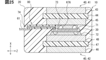
- the semiconductor module 10 includes wiring members 80 .
- Wiring member 80 provides at least one signal path.
- the wiring member 80 is also called a wiring sheet.
- the wiring member 80 is housed in the resin member 20 .
- the wiring member 80 is plate-shaped.
- the wiring member 80 includes an electrically insulating resin layer and a metal layer supported by the resin layer.
- the wiring member 80 includes one metal layer or multiple metal layers.
- the thickness of the wiring member 80 is equal to or less than the thickness of the first joint member 71 .
- the wiring member 80 extends substantially parallel along the YZ plane so as to intersect the thickness direction X. As shown in FIG.
- the wiring member 80 is a member that is more flexible than the signal terminal 61 . Due to its flexibility, the wiring member 80 may be arranged in a slightly bent shape.
- the wiring member 80 electrically connects the signal pad of the semiconductor element 30 and the signal terminal 61 .
- the wiring member 80 is positioned and fixed by bonding at the bonding portions 80 a and 80 b and contact with the resin member 20 .
- the wiring member 80 is completely embedded in the resin member 20 and is not exposed to the outside.
- the wiring member 80 may be provided by a flexible printed circuit board (FPC).
- the wiring member 80 may be provided by single-sided FPC, double-sided FPC, or multilayer FPC.
- the resin layer can be provided by polyimide resin, liquid crystal polymer resin (LPC), or the like, as non-limiting examples.
- the metal layer can be provided by copper foil, silver paste, or the like, as non-limiting examples.
- the wiring member 80 enables various arrangements such as approach, dispersion, and detour for one metal layer. Moreover, the wiring member 80 enables various variations also regarding the area of the metal layer. Furthermore, the wiring member 80 provides stable electrical insulation between the electrical connection provided by the wiring member 80 and other adjacent members by means of the resin layer. In a typical example, one wiring member 80 includes multiple metal layers. The metal layers provide electrical connections between signal pads and signal terminals 61 . In this case, the wiring member 80 enables reduction of process time in the manufacturing stage for providing multiple electrical connections. Additionally, in this case, the wiring member 80 provides stable electrical insulation between multiple electrical connections. The wiring member 80 allows the metal layers to be arranged through various paths inside the wiring member 80 .
- the wiring member 80 enables various arrangements such as crossing, connection, and branching with respect to a plurality of metal layers. Furthermore, the plurality of metal layers are fixedly held in positional relationship with each other by the resin layer. This results in less variation in mutual coupling inductance between signal paths than wire bonding. As a result, the wiring member 80 contributes to stable driving of the semiconductor element 30 .
- the resin member 20 accommodates the semiconductor element 30 .
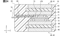
- the semiconductor element 30 is joined to the heat dissipation member 40 by joining members 70 on both surfaces thereof.
- the joint member 70 has a flat polygonal prism shape.
- the joining member 70 has a columnar shape with a slightly trapezoidal cross section. This junction provides an electrical connection and a thermal coupling.
- the semiconductor element 30 has power pads 33 on its first surface, which is the top surface in the drawing. Power pads 33 provide the main power path controlled by this semiconductor device 30 .
- the power pad 33 is joined to the first heat dissipation member 41 by the first joining member 71 .
- Semiconductor device 30 has power pads 34 on its second surface, which is the bottom surface in the figure. Power pads 34 provide the main power path controlled by this semiconductor device 30 .
- the power pad 34 is joined to the second heat dissipation member 42 by a second joining member 72 .
- the power pads 33 and 34 may be called by names indicating their uses, such as power electrodes, collector electrodes, and emitter electrodes.
- the joining member 70 can be provided by a material called so-called solder.
- the heat dissipation member 40 has a flat plate shape.
- the heat dissipation member 40 provides high thermal conductivity (more precisely, heat transfer coefficient) between its two surfaces.
- the heat dissipation member 40 is also called a terminal member that provides a power path.
- the heat dissipation member 40 provides high electrical insulation between its two surfaces.
- the heat dissipation member 40 is also called an electrically insulating substrate.
- the heat dissipation member 40 includes an electrically insulating resin plate arranged between a pair of metal plates.
- the first heat dissipation member 41 includes an external metal plate 43 that provides a heat dissipation surface and an internal metal plate 45 that provides a joint surface.
- An internal metal plate 45 provides a portion of the power path.
- the inner metal plate 45 is electrically joined to one terminal that provides the power line 50 .
- At least a partial surface of the external metal plate 43 is exposed outside from the resin member 20 .
- One surface of the external metal plate 43 provides a heat dissipation surface.
- the first heat radiating member 41 includes a resin plate 44 as an electrical insulating layer arranged between an external metal plate 43 and an internal metal plate 45 .
- the second heat dissipation member 42 includes an outer metal plate 46 that provides a heat dissipation surface and an inner metal plate 48 that provides a joint surface.
- An internal metal plate 48 provides a portion of the power path.
- the inner metal plate 48 is electrically joined to one terminal that provides a power line 50 .
- At least a partial surface of the external metal plate 46 is exposed outside from the resin member 20 .
- One surface of the outer metal plate 46 provides a heat dissipation surface.
- the second heat radiating member 42 includes a resin plate 47 as an electrical insulation layer arranged between an external metal plate 46 and an internal metal plate 48 .
- the semiconductor element 30 has signal pads 35 on the first surface.
- the signal pads 35 are located at the outer edge of the semiconductor device 30 so as to allow the formation of relatively large area power pads 33 on the first surface.
- the signal pad 35 has a significantly smaller conducting area than the power pads 33,34.
- semiconductor device 30 has a plurality of signal pads 35 .
- the signal pad 35 may be called by a name indicating its use, such as a signal electrode, a sensor electrode, or a gate electrode.
- the wiring member 80 is positioned apart from the heat dissipation member 40 .
- the wiring member 80 may be arranged in contact with the surface of the semiconductor element 30 .
- the signal pad 35 and signal terminal 61 are electrically connected by a wiring member 80 .
- the wiring member 80 is arranged inside the resin member 20 so as to bridge between the signal pad 35 and the signal terminal 61 .
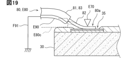
- the wiring member 80 has a resin layer 81 made of an electrically insulating resin material.
- the wiring member 80 has a resin layer 83 made of an electrically insulating resin material.
- the resin layer 81 and the resin layer 83 may be made of a continuous resin material.
- the wiring member 80 may be coated with an electrically insulating film on the outside of the resin layers 81 and 83 . The insulating coating contributes to enhancing electrical insulation between the wiring member 80 and other components.
- the wiring member 80 has a metal layer 82 arranged between the resin layer 81 and the resin layer 83 .
- the metal layer 82 is arranged on the wiring member 80 in a linear or ribbon-like form.
- Metal layer 82 is made of metal.
- the metal layer 82 may also be called a current-carrying member or signal line for signal transmission.
- the metal layer 82 is continuously arranged from one end to the other end.
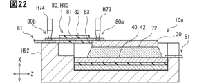
- the wiring member 80 has a first joint portion 80 a for enabling electrical connection between the metal layer 82 and the signal pad 35 .
- the second joint portion 80 b is provided at one end of the metal layer 82 .
- the wiring member 80 has a second joint portion 80 b for enabling electrical connection between the metal layer 82 and the signal terminal 61 .
- the second joint portion 80 b is provided at the other end of the metal layer 82 .
- the first joint portion 80 a and the second joint portion 80 b are separated by windows formed in the resin layers 81 and 83 . The window exposes a portion of the metal layer 82 from the resin layers 81 and 83 .
- the first joint portion 80 a and the second joint portion 80 b may be grasped as part of the metal layer 82 .
- the signal pad 35 of the semiconductor element 30 and one end of the metal layer 82 are electrically connected to each other by the third bonding member 73 at the first bonding portion 80a.
- the other end of the metal layer 82 and the signal terminal 61 are electrically connected by a fourth joint member 74 at the second joint portion 80b.
- FIG. 4 is a partial cross-sectional view taken along line IV-IV in FIG. 3 with the resin member 20 removed.
- the heat dissipation member 40, the semiconductor element 30, the wiring member 80, and the signal terminal 61 are arranged in layers in the X direction.
- the heat dissipation member 40, the semiconductor element 30, the wiring member 80, and the signal terminal 61 are in a parallel relationship.
- the heat dissipation member 40 and the semiconductor element 30 are arranged in parallel so as to overlap each other.
- the semiconductor element 30 and the wiring member 80 are arranged in parallel so as to overlap only at the first joint portion 80a.
- the wiring member 80 and the signal terminal 61 are arranged in parallel so as to overlap only at the second joint portion 80b.
- the heat dissipation member 40, the semiconductor element 30, the wiring member 80, and the signal terminal 61 are plate-shaped.
- the heat dissipation member 40, the semiconductor element 30, the wiring member 80, and the signal terminal 61 are arranged so that the surface as a plate is parallel to the YZ plane. Therefore, the signal terminal 61 extends from the side surface of the resin member 20 in parallel with the YZ plane.
- the semiconductor element 30 is placed on and bonded to the second heat dissipation member 42 .
- the power pad 33 of the semiconductor element 30 is joined to the first heat dissipation member 41 (not shown) by the first joining member 71 .
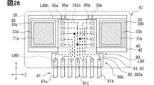
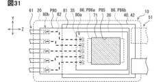
- Semiconductor device 30 has a plurality of signal pads 35 .
- power pads 33 and signal pads 35 are represented by rectangular shapes.
- the pads of the semiconductor device 30 can be provided in various shapes such as circles, ovals, rounded polygons, and polygons.
- the plurality of signal pads 35 are arranged apart from each other on the outer edge of the upper surface of the semiconductor element 30 .
- a plurality of signal pads 35 are arranged in rows along the outer edge.
- the plurality of signal pads 35 may be arranged at the corners of the top surface of the semiconductor element 30 .
- the plurality of signal pads 35 may be dispersedly arranged on the upper surface of the semiconductor element 30 so as to form a plurality of groups.
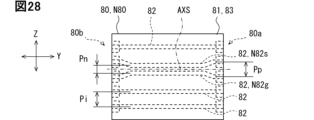
- a plurality of signal pads 35 are arranged with a pad pitch Pp.
- Pad pitch Pp is the minimum pad pitch among the plurality of signal pads 35 .
- a plurality of signal pads 35 are arranged within a range of width Wp.
- the plurality of signal terminals 61 have a shape that can be called an elongated rod shape or a ribbon shape.
- the plurality of signal terminals 61 are arranged parallel to each other. One ends of the plurality of signal terminals 61 are arranged in a straight line.
- the multiple signal terminals 61 may have different thicknesses.
- the multiple signal terminals 61 may have different lengths.
- a plurality of signal terminals 61 are arranged with a terminal pitch Pi.
- the terminal pitch Pi is the minimum terminal pitch among the plurality of signal terminals 61 .
- the plurality of signal terminals 61 are arranged within a width Wi.
- the terminal pitch Pi is greater than or equal to the pad pitch Pp (Pi ⁇ Pp).
- the terminal pitch Pi is larger than the pad pitch Pp (Pi>Pp).
- Terminal pitch Pi and pad pitch Pp are different.
- the wiring member 80 is arranged between the signal pad 35 and the signal terminal 61 .
- the wiring member 80 is arranged to bridge the plurality of signal pads 35 and the plurality of signal terminals 61 .
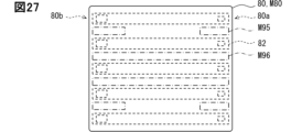
- the wiring member 80 has resin layers 81 and 83 and a metal layer 82 .
- the wiring member 80 has a plurality of metal layers 82 that are electrically independent of each other. Each of the plurality of metal layers 82 electrically connects each of the plurality of signal pads 35 and each of the plurality of signal terminals 61 .
- the plurality of metal layers 82 are insulated from other members by resin layers 81 and 83 at portions other than the joint portions 80a and 80b.
- the wiring member 80 has a first joint portion 80 a for connecting the metal layer 82 and the signal pad 35 .
- the first joint portion 80 a is formed by exposing the metal layer 82 from the resin layer 81 and/or the resin layer 83 .
- the first joint portion 80a is formed by a window portion defined by the resin layer 81 and/or the resin layer 83 and an exposed portion of the metal layer 82 exposed through the window portion.
- the window portion is an opening having a predetermined area in the resin layer 81 and/or the resin layer 83 .
- the exposed portion has an area and shape that can be bonded to the signal pad 35 .
- the wiring member 80 has a second joint portion 80 b for connecting the metal layer 82 and the signal terminal 61 .
- the second joint portion 80 b is formed by exposing the metal layer 82 from the resin layer 81 and/or the resin layer 83 .
- the second joint portion 80b is formed by a window portion defined by the resin layer 81 and/or the resin layer 83 and an exposed portion of the metal layer 82 exposed through the window portion.
- the window portion is an opening having a predetermined area in the resin layer 81 and/or the resin layer 83 .
- the exposed portion has an area and shape that can be joined to the signal terminal 61 .
- the laying paths of the plurality of metal layers 82 in the wiring member 80 are set to provide electrical connection while allowing the difference Dp and/or the difference Dw.
- the width Wi on the signal terminal 61 side is wider than the width Wp on the signal pad 35 side.
- the shape of the wiring member 80 is also set to provide electrical connection while allowing for the difference Dp and/or the difference Dw.
- the width of the wiring member 80 itself is wider at the end on the signal terminal 61 side than at the signal pad 35 side.
- the shapes of the plurality of metal layers 82 on the YZ plane are substantially parallel to each other. However, the shape of the multiple metal layers 82 in the YZ plane is formed so that the difference between the width Wi and the width Wp is absorbed by the change in the distance between the multiple metal layers 82 .
- the shapes of the metal layers 82 are set to vary the distance between them.
- the distance between multiple metal layers 82 may also be referred to as metal layer pitch.
- the metal layer pitch is equal to the terminal pitch Pi on the signal terminal 61 side.
- the metal layer pitch is equal to the pad pitch Pp on the signal pad side.
- the metal layer pitch decreases from terminal pitch Pi to pad pitch Pp. In the illustrated example, the metal layer pitch changes stepwise. Alternatively, the metal layer pitch may vary gradually.
- the manufacturing method of the semiconductor module 10 has a preparation step of preparing a plurality of parts.
- a preparation process is a process of preparing main components.
- the preparatory process includes the material of the resin member 20 before molding, the semiconductor element 30, the heat dissipation member 40, the lead frame that provides the power terminals 51, the lead frame that provides the signal terminals 61, the joining member 70, and the wiring. and providing a member 80 .
- the manufacturing method of the semiconductor module 10 has a bonding step of electrically and/or thermally and mechanically bonding a plurality of components.
- the bonding process includes a semiconductor bonding process of bonding the heat radiating member 40 and the semiconductor element 30 with the bonding members 71 and 72 .
- the semiconductor bonding step includes a first bonding member step of bonding the first heat dissipation member 41 and the semiconductor element 30 with the first bonding member 71 .
- the semiconductor bonding step includes a second bonding member step of bonding the second heat dissipation member 42 and the semiconductor element 30 with the second bonding member 72 .
- the first joining member step may be performed after the second joining member step.
- the second joining member step may be performed after the first joining member step.
- the first joining member step and the second joining member step may be performed simultaneously.
- the bonding process includes a power terminal bonding process for bonding the heat radiating member 40 and the power terminals 51 .
- the bonding process includes a signal path bonding process of connecting the signal pad 35 and the signal terminal 61 via the wiring member 80 .
- the signal path bonding step includes a third bonding member step of bonding the signal pad 35 and the wiring member 80 with the third bonding member 73 .
- the signal path joining step includes a fourth joining member step of joining the signal terminal 61 and the wiring member 80 with the fourth joining member 74 .
- the third joining member step and the fourth joining member step can be performed simultaneously.
- the third joining member step and the fourth joining member step may be performed in numerical order or in reverse numerical order.
- the semiconductor bonding process and the signal path bonding process can be performed simultaneously. Furthermore, simultaneously with these, a power terminal bonding step may be performed.
- the semiconductor bonding process, the power terminal bonding process, and the signal path bonding process for example, when solder is used as the bonding member 70, can be performed by a temporary heating process that melts and rehardens the solder.
- a temporary heating process that melts and rehardens the solder.
- at least the second bonding member step and the third bonding member step and/or at least the second bonding member step and the fourth bonding member step may be performed simultaneously by a temporary heating step.
- the second heat radiation member 42, the second bonding member 72, and the semiconductor element 30 are arranged in a layered manner in the arrangement step preceding the heating step.
- the signal pad 35, the third joint member 73, and the first joint portion 80a are arranged in layers.
- the signal terminal 61, the fourth joint member 74, and the second joint portion 80b are arranged in layers.
- the heating step by melting the bonding members 72 , 73 , 74 , bonding between the semiconductor element 30 and the second heat radiation member 42 and bonding of the wiring member 80 can be performed simultaneously.
- the semiconductor element 30, the first bonding member 71, and the first heat radiation member 41 may be arranged in a stacked manner. In this case, the joining members 71, 72, 73, and 74 are simultaneously melted in the heating process.
- a bonding process is performed to bond all joints.
- the bonding step includes a curing step of curing the bonding member. A plurality of members are joined by the joining step.
- the manufacturing method of the semiconductor module 10 has a resin molding step of wrapping the intermediate product joined by the joining step with the resin member 20 .
- the resin molding process is carried out in such a way that the interstices between the parts of the intermediate product are penetrated by the resin parts to provide the intended electrical insulation.
- the resin molding process is a process of exposing the heat dissipation member 40 , the power terminals 51 , and the signal terminals 61 and molding the resin member 20 so as to cover the semiconductor element 30 .
- the resin molding process includes an arrangement process of arranging the joined parts in a mold.
- the resin molding process includes an injection process of injecting the molten resin member 20 into a mold.
- the resin molding process includes a curing process for curing the molten resin member 20 .
- the resin molding step includes a removal step of removing the molded product from the mold.
- the resin molding process further includes a finishing process including a process of cutting the lead frame and a process of removing resin burrs.
- the wiring member 80 provides electrical connection between the signal pads 35 of the semiconductor element 30 and the signal terminals 61 .
- the wiring member 80 enables an easy joining process.
- the wiring member 80 itself has electrical insulation due to the resin layers 81 and 83 . Therefore, the wiring member 80 improves the reliability of electrical insulation between the metal layer 82 and other members.
- the wiring member 80 has a plurality of metal layers 82, reliability of electrical insulation between the plurality of metal layers 82 is improved.
- the wiring member 80 is wrapped, fixed, and supported by the resin member 20 . Therefore, foreign matter is prevented from entering the semiconductor module 10 from the outside. Foreign matter includes liquid such as water, corrosive gas, and the like. In other words, the wiring member 80 and the resin member 20 provide high sealing performance.
- This embodiment is a modification based on the preceding embodiment.
- the plurality of signal pads 35 are distributed along one short side of the semiconductor element 30 .
- this embodiment employs a plurality of signal pads 235 centrally located on a portion of the semiconductor device 30 . It is desirable that the semiconductor element 30 has a relatively large active region that exhibits activity as a switching element. A relatively large active area allows control of large currents.
- This embodiment provides a semiconductor device 30 that allows for a relatively large active area.
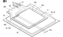
- FIG. 5 shows a perspective view of a plurality of parts with the resin member 20 and the first heat radiation member 41 removed.
- the semiconductor element 30 is plate-shaped with a rectangular surface.
- the semiconductor element 30 is approximately square.
- the semiconductor element 30 has a plurality of signal pads 235 in a rectangular area near the corners of the outer edge of the surface.
- a plurality of signal pads 235 are concentrated in a rectangular area.
- a plurality of signal pads 235 are arranged in a row along the outer edge of the surface.
- a plurality of signal pads 235 are arranged with a pad pitch Pp2 in the column direction.
- the pad pitch Pp2 is smaller than the pad pitch Pp of the previous embodiment.
- the pad pitch Pp2 is set to a numerical value that can be called minute compared to the size of the semiconductor element 30 .
- the wiring member 80 has a plurality of first joints 80a and a plurality of second joints 80b.
- Each of the plurality of first joints 80 a is joined to each of the plurality of signal pads 235 . Therefore, the plurality of signal pads 35 are arranged to form a pad pitch Pp2 in the column direction.
- the plurality of second joint portions 80b are arranged to form a terminal pitch Pi in the column direction.
- Each of the multiple second joint portions 80 b is joined to each of the multiple signal terminals 61 .
- the plurality of metal layers 82 are arranged so as to expand the fine pad pitch Pp2 to the terminal pitch Pi.
- a plurality of metal layers 82 are laid so as to meander between the first joint portion 80a and the second joint portion 80b.
- the wiring member 80 has an outer edge portion 284 arranged along the outer edge of the surface of the semiconductor element 30 where the plurality of signal pads 235 are not arranged.
- the outer edge 284 is arranged along the longitudinal direction of the outer edge.
- the outer edge portion 284 is arranged on three outer edge portions where the signal pads 235 are not arranged among the four outer edge portions of the surface of the semiconductor element 30 .
- the wiring members 80 are arranged on the surface of the semiconductor element 30 so as to surround the power pads 33 through which the main current flows. In other words, the wiring member 80 is arranged so as to surround the first joint member 71 .
- the wiring member 80 defines the opening 285 .
- the outer edge portion 284 is formed only with the resin layer 81 or the resin layer 83 .
- Outer edge 284 may include metal layer 82 .
- the outer edge portion 284 facilitates positioning of the wiring member 80 with respect to the semiconductor element 30 . As a result, even with a fine pad pitch Pp2, the plurality of signal pads 235 and the plurality of first joint portions 80a can be accurately and easily positioned.
- the outer edge portion 284 improves electrical insulation at the outer periphery of the semiconductor element 30 .
- the wiring member 80 improves electrical insulation between a member such as an electrode as a power path of the semiconductor element 30 and a portion such as an electrode as a signal path.
- the outer edge portion 284 may define the shape of the first joint member 71 .
- the fine pad pitch Pp2 makes it possible to relatively reduce the area occupied by the plurality of signal pads 235 .
- the area of the semiconductor element 30 occupied by the bonding member 70 and/or the area of the active region for current flow can be relatively increased.
- the active region extends substantially over the range where the first bonding member 71 is arranged.
- the active region extends adjacent to all four sides of semiconductor device 30 .
- One side of the semiconductor element 30 is shared by the area occupied by the plurality of signal pads 235 and the area occupied by the active region.
- the range occupied by the plurality of signal pads 235 is a range of two thirds or less of one side of the semiconductor element 30, or a range of one half or less.
- the fine pad pitch Pp2 makes it possible to suppress current density and/or improve heat conductivity by increasing the area of the bonding member 70 occupying the surface of the semiconductor element 30 .
- the fine pad pitch Pp2 makes it possible to suppress current density and/or improve heat conductivity by increasing the area of the bonding member 70 occupying the surface of the semiconductor element 30 .
- one semiconductor module 10 includes one semiconductor element 30 .
- one semiconductor module 10 can include two or more semiconductor elements. This embodiment is an example of a case where a plurality of semiconductor elements are provided. This embodiment provides a semiconductor module 10 containing multiple semiconductor devices 30 arranged in parallel or in series.
- two semiconductor elements 30a and 30b are arranged in a layered manner with respect to the second heat dissipation member 42.
- the two semiconductor elements 30a and 30b have the same shape or similar shapes.
- the two semiconductor elements 30 a and 30 b are arranged rotationally symmetrically on the second heat dissipation member 42 .
- two semiconductor devices 30a, 30b are arranged in parallel in the power path.
- the semiconductor device 30a has a power pad 33a and a plurality of signal pads 35a.
- the semiconductor element 30a and the bonding member 71a are arranged in layers.
- the semiconductor device 30b has a power pad 33b and a plurality of signal pads 35b.
- the semiconductor element 30b and the bonding member 71b are arranged in layers.
- the two semiconductor elements 30a, 30b may be arranged in series in the power path.
- one of the semiconductor elements 30a and 30b may be used as an upper arm, and the other of the semiconductor elements 30a and 30b may be used as a lower arm.
- one semiconductor module 10 provides one switching arm 18 .
- the wiring member 80 is provided by the wiring member 380.
- the wiring member 380 includes a plurality of first joints 80a for the semiconductor elements 30a.
- the wiring member 380 includes a plurality of first joints 80a for the semiconductor elements 30b.
- the wiring member 380 includes a common second joint portion 80b for the plurality of semiconductor elements 30a, 30b.
- the plurality of metal layers 82 has separate metal layers 382a and common metal layers 382c.
- a separate metal layer 382a is bonded to only one of the plurality of signal pads 35a, 35b.
- the common metal layer 382c is commonly bonded to one signal pad 35a of the semiconductor element 30a and one signal pad 35b of the semiconductor element 30b.
- the metal layers 382a and 382c are bonded to the signal terminal 61 at the second bonding portion 80b.
- the plurality of signal terminals 61 includes a dedicated signal terminal 61a for only the semiconductor element 30a, a dedicated signal terminal 61b for only the semiconductor element 30b, and a signal terminal 61c common to the semiconductor elements 30a and 30b.
- the dedicated signal terminals 61a and 61b are used as sensor terminals for the temperature and current of the semiconductor elements 30a and 30b.
- the common signal terminal 61c is used as a gate terminal or the like for driving the plurality of semiconductor elements 30a and 30b at the same timing.
- dedicated signal terminals 61 a and 61 b are arranged on both sides of the row of the plurality of signal terminals 61
- a common signal terminal 61 c is arranged in the central portion of the row of the plurality of signal terminals 61 .
- the wiring member 80 can provide a dedicated connection and a common connection inside the wiring member 80 by providing an independent metal layer 382a and a common metal layer 382c.
- the wiring member 80 can correspond to different arrangements of the plurality of signal pads 35a and 35b.
- the arrangement of the dedicated signal terminals 61a and 61b and the common signal terminal 61c can be changed.
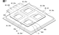
- This embodiment is a modification based on the preceding embodiment.
- This embodiment is an example of a case where a plurality of semiconductor elements are provided.
- One semiconductor module 10 includes a plurality of semiconductor elements 30a, 30b, 30c, and 30d.
- FIG. 7 four semiconductor elements 30a, 30b, 30c, and 30d are stacked in parallel with respect to the second heat dissipation member .
- a plurality of semiconductor elements 30 have the same shape or a similar shape.
- the plurality of semiconductor elements 30 are arranged such that the signal pads 35 are positioned on one side of the second heat dissipation member 42 .
- the plurality of semiconductor elements 30 are dispersedly arranged in a grid pattern.
- the wiring member 80 is provided by the wiring member 480 .
- the wiring member 480 has an area extending over the plurality of semiconductor elements 30a, 30b, 30c, and 30d.
- the wiring member 480 has an outer edge portion 484 and an opening portion 485 .
- the outer edge portion 484 extends like a lattice.
- the wiring member 480 has four openings 485 .
- Each of the four openings 485 opens at a position corresponding to each of the four semiconductor elements 30 .
- the opening 485 provides an opening for the first joint member 71 to pass through.
- the wiring member 480 has multiple metal layers 82 .
- the plurality of metal layers 82 includes dedicated metal layers 82a and common metal layers 82c.
- the metal layer 82 is laid around the semiconductor element 30 to continuously extend between the first joint portion 80a and the second joint portion 80b.
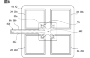
- This embodiment is a modification based on the preceding embodiment.
- This embodiment is an example of a case where a plurality of semiconductor elements are provided.
- One semiconductor module 10 includes a plurality of semiconductor elements 30a, 30b, 30c, and 30d.
- FIG. 8 four semiconductor elements 30a, 30b, 30c, and 30d are arranged in a square. Moreover, the four semiconductor elements 30a, 30b, 30c, and 30d are arranged rotationally symmetrically with respect to the central axis AXC. Each of the plurality of semiconductor elements 30 has a signal pad 35 positioned at a corner. The plurality of semiconductor elements 30 are arranged such that the signal pads 35 are positioned near the center axis AXC.
- the wiring member 80 is provided by a wiring member 580.
- the wiring member 580 has a metal layer 82c.
- the wiring member 580 includes four first joints 80a.
- the wiring member 580 includes a second joint portion 80b connected to a common terminal member.
- the metal layer 82c has a portion extending between the second joint portion 80b and the central axis AXC, and a plurality of branched portions extending radially from the central axis AXC and reaching the first joint portion 80a.
- a common metal layer 82c provides common electrical connections to the plurality of semiconductor devices 30a, 30b, 30c, 30d.
- a common metal layer 82c provides approximately equal length signal paths to the plurality of signal pads 35 from the second junction 80b.
- a substantially equal length means that the electrical characteristics are substantially equal, or that any difference is substantially negligible due to the nature of the signal.
- signal pad 35 may be a pad for drive signals such as gate signals. In this case, it is possible to suppress the difference in drive signals applied to the plurality of semiconductor elements 30 .
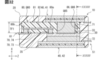
- the wiring member 80 is positioned away from the heat dissipation member 40 .
- the wiring member 680 is arranged in contact with both the semiconductor element 30 and the first heat radiation member 41 .
- the wiring member 680 has a recess 86 .
- the concave portion 86 functions as a volume adjustment portion for adjusting the volume of the first bonding member 71 to an appropriate amount for bonding the power pad 33 of the semiconductor chip 30 and the first heat radiation member 41 .
- Recess 86 is provided by recess 686 .
- This embodiment provides the semiconductor module 10 capable of stabilizing the physical size of the first joint member 71 .
- the semiconductor module 10 includes the semiconductor element 30 arranged between the first heat dissipation member 41 and the second heat dissipation member 42. As shown in FIG. The semiconductor module 10 includes wiring members 680 . Wiring member 80 is provided by wiring member 680 . The wiring member 680 is positioned between the semiconductor element 30 and the first heat radiation member 41 . The wiring member 680 is arranged in contact with both the semiconductor element 30 and the first heat radiation member 41 . The wiring member 680 electrically connects the signal pad 35 of the semiconductor element 30 and the signal terminal 61 .
- the wiring member 680 has resin layers 81 and 83 . Each of the resin layers 81 and 83 is formed by an assembly in which a plurality of resin layers are arranged in a laminated manner. In addition, the resin layers 81 and 83 may be formed of a single resin layer formed of a continuous resin material.
- the wiring member 680 has an outer edge portion 684 arranged along the edge of the first joint member 71 .
- the outer edge portion 684 surrounds the first joining member 71 in the YZ plane.
- the outer edge 684 defines an opening 685 that defines the position and maximum extent of the first joining member 71 in the YZ plane.
- the wall surface of the opening 685 may form a minute gap with the first joint member 71 and may come into contact with the first joint member 71 .
- the opening 685 defines the range of the first joint member 71 .
- the wiring member 680 has a concave portion 686 .
- the recess 686 is open to the wall surface that defines the opening 685 .
- the concave portion 686 is formed by a notch that penetrates at least one of the resin layers forming the resin layers 81 and 83 . Therefore, the recess 686 has a thickness in the X direction corresponding to at least one resin layer.
- the recess 686 is provided by the resin layer located at the endmost of the plurality of resin layers. Therefore, the recess 686 is also open to the end face of the wiring member 680 in the X direction (thickness direction).
- Recess 686 defines an expansion chamber communicating with opening 685 .
- a recess 686 provides the side wall of the expansion chamber.
- the walls of the expansion chamber in the X direction are provided by another resin layer.
- Recess 686 is positioned only on a portion of the wall of opening 685 .
- the recess 686 has a shape that can be called a notch of the wiring member 680 .
- Recess 686 expands the volume of opening 685 in only a portion of the YZ plane.
- Recess 686 expands the volume of opening 685 in only a portion of the XZ plane.
- a volume expansion chamber defined by recess 686 may accommodate an excess portion of first joining member 71 .
- An excess portion of the first joint member 71 flows out into the recess 686 by being extruded or by its own fluidity, hardens, and remains in the recess 686 .
- the figure shows the excess portion 675 remaining in the recess 686 .
- the volume expansion chamber functions as a relief capacity for absorbing the excessive amount of the first joint member 71 when there is an excessive amount of the first joint member 71 in the opening 685 .
- the recessed portion 686 is arranged so as to partition the extended volume chamber by part of the surface of the first heat radiation member 41 .
- the recess 686 is positioned adjacent to the first heat radiation member 41 .
- the recesses 686 are provided only in some of the many resin layers. In the illustrated example, the recess 686 is provided only in the resin layer closest to the first heat radiation member 41 . As a result, one surface of the expanded volume chamber provided by the recess 686 is defined by the first heat radiation member 41 .
- the recess 686 is provided so as not to reach the metal layer 82 .
- the concave portion 686 is formed so as to maintain good electrical insulation between the first bonding member 71 and the metal layer 82 . Recess 686 is provided to provide a predetermined electrical isolation distance from metal layer 82 .
- the wiring member 680 has a thickness TF1.
- the thickness TF1 is the thickness with which the wiring member 80 is in contact with the surface of the semiconductor element 30 and the first heat radiation member 41 .
- the thickness TF ⁇ b>1 is a thickness that defines the thickness of the first joint member 71 and is equal to the thickness of the first joint member 71 .
- the manufacturing method of the semiconductor module 10 has a first bonding step of bonding the first heat radiation member 41 and the semiconductor element 30 with the first bonding member 71 .
- the manufacturing method has an arrangement step before the first bonding step.
- the first heat dissipation member 41, the wiring member 680, and the semiconductor element 30 are arranged in a stacked manner.
- the first bonding member 71 before bonding (before melting and re-hardening) is placed in the opening 685 .
- the first joint member 71 in the placement step has a thickness equal to or greater than the thickness TF1.
- the first bonding process is performed.
- the first joining member 71 melts and flows.
- the first bonding member 71 bonds the first heat radiation member 41 and the semiconductor element 30 and is cured again.
- the thickness of the first bonding member 71 changes during the process of melting and hardening the first bonding member 71 again. In many cases, the thickness of the first bonding member 71 decreases from before the bonding process to after the bonding process.
- pressure may be applied in a direction to bring the first heat radiation member 41 and the semiconductor element 30 closer together. This pressure also reduces the thickness of the first joining member 71 .
- the wiring member 680 contacts the first heat radiation member 41 and the semiconductor element 30 .
- the opening 685 suppresses the flow of the first joint member 71 . If the first bonding member 71 is excessively present in the process of melting and hardening the first bonding member 71, the distance between the first heat radiation member 41 and the semiconductor element 30 may not be stable. At this time, the excess portion of the first joint member 71 is pushed out toward the recess 686 . The excess portion of the first joining member 71 may flow into the recess 686 without being pushed out. The excess portion of the first joining member 71 remains in the recess 686 as the excess portion 675 by hardening again. As a result, excess portion 675 is retained within recess 686 . It can be said that the recess 686 provides relief capacity for the first joint member 71 .
- the recess 686 is adjacent to the first heat radiation member 41 . Therefore, the excess portion 675 contacts the first heat radiating member 41 and contributes to providing a wide cross-sectional bonding area. Providing a wide joint cross-sectional area enhances the heat transfer in the first joint member 71 and makes it possible to suppress the current density.
- gas components may be mixed in the first joining member 71, or gas components may be generated when the first joining member 71 melts.
- Recesses 686 may receive these gaseous components.
- the gas component may create voids inside the first bonding member 71 that has hardened again.
- the flow of the gas component into the recess 686 may suppress the generation of voids in the first bonding member 71 . It can be said that the recess 686 provides an escape capacity for gaseous components during the bonding process.
- the volume provided by the recess 686 is provided as an additional volume to the standard volume for the first joining member 71 provided by the opening 685.
- the first joint member 71 attempts to overflow the standard volume, the first joint member 71 flows into the additional volume provided by the recess 686 .
- the first bonding member 71 may remain in the additional volume provided by the recess 686 .
- an appropriate volume of first joint member 71 remains in the standard volume provided by opening 685 .
- the first bonding member 71 remaining in the opening 685 provides a proper bonding state between the semiconductor chip 30 and the first heat radiation member 41 .
- the concave portion 686 suppresses inclination between the semiconductor element 30 and the first heat radiation member 41 , unstable bonding, and unintended leakage of the first bonding member 71 .
- the entire wiring member 680 has a thickness TF1.
- the wiring member 680 may be configured to have the thickness TF ⁇ b>1 only in the portion positioned between the semiconductor element 30 and the first heat radiation member 41 .
- the wiring member 680 may be configured to have a thickness smaller than the thickness TF1 at the portion arranged to bridge between the semiconductor element 30 and the signal terminal 61 . Such a configuration provides the flexibility required for the portion positioned to bridge between semiconductor device 30 and signal terminal 61 .
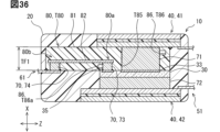
- this embodiment is a modification based on the preceding embodiment.
- the metal layer 82 of the wiring member 80 only connects the signal pad 35 and the signal terminal 61 .
- the wiring member 780 comprises a metal layer 787 bonded to the first bonding member 71 . From one point of view, this embodiment provides a semiconductor module 10 in which the thickness of the joint member can be stably adjusted to a predetermined value. From another point of view, this embodiment provides the semiconductor module 10 in which the position of the wiring member 780 can be stably set.
- wiring member 80 is provided by wiring member 780 .
- the wiring member 780 is arranged between the signal pad 35 and the signal terminal 61 .
- the wiring member 780 is arranged so as to overlap the signal pad 35 in the X direction.
- the wiring member 780 is arranged so as to overlap with the power pad 33 in the X direction.
- the wiring member 780 extends so as to overlap both the signal pad 35 and the power pad 33 . In other words, the wiring member 780 extends to the area where the first joint member 71 is arranged.
- the wiring member 780 has an outer edge portion 784 arranged along the first joint member 71 .
- the outer edge portion 784 surrounds the range where the first joint member 71 is to be installed.
- the outer edge portion 784 defines an opening 785 in the resin layers 81 and 83 corresponding to the range of the first joint member 71 .
- Wiring member 780 includes metal layer 787 exposed in opening 785 .
- the opening 785 is also called a notch for exposing the metal layer 787 from the resin layers 81 and 82 .
- the metal layer 787 is made of the same material as the metal layer 82 .
- the metal layer 787 that provides the power path is electrically isolated from the metal layer 82 that provides the signal path.
- the metal layer 787 is exposed from the wiring member 780 over at least the region of the first bonding member 71 on the YZ plane.
- the metal layer 787 is arranged in the first joint member 71 and joined. As a result, the metal layer 787 partitions the first joining member 71 into the first layer 71c and the second layer 71d.
- the first layer 71 c bonds the power pads 33 of the semiconductor device 30 and the metal layer 787 .
- the second layer 71 d joins the metal layer 787 and the first heat dissipation member 41 .
- the metal layer 787 is embedded inside the first bonding member 71 .
- the metal layer 787 or the opening 785 may have a communication opening for forming the first layer 71c and the second layer 71d as a continuous joining member.
- the openings 785 can form communicating openings between the resin layers 81 , 83 and the metal layer 787 .
- the metal layer 787 can have cutouts or holes as communicating openings communicating between both sides of the metal layer 787 .
- the metal layer 787 is positioned so as to be embedded in the first joining member 71 .
- the position of the wiring member 780 is stabilized by the first joint member 71 .
- the wiring member 780 receives resin flow and resin pressure in the molding process of molding the resin member 20 .
- the wiring member 780 in which the metal layer 787 is embedded in the first bonding member 71 is difficult to deform even in the molding process and maintains a predetermined shape.
- the wiring member 780 is less likely to warp and deform even if it receives pressure from the resin.
- a thickness adjustment member 776 is arranged between the metal layer 787 and the first heat radiation member 41 to adjust the thickness of the first layer 71c.
- the thickness adjustment member 776 may be provided by nickel balls (Ni balls), bonding pads, wire bonding, or the like.
- the thickness adjusting member 776 is provided by a conductive member that functions as the first joining member 71 together with the first layer 71c, or by a conductive metal member.
- the thickness adjusting member 776 is also arranged between the metal layer 787 and the semiconductor element 30 . The thickness adjusting member 776 contributes to adjusting the thickness of the first layer 71c and the second layer 71d to a predetermined thickness.
- the wiring member 80 is plate-like providing a continuous surface. From one point of view, the plate-shaped wiring member 80 may affect the flow of the resin, such as obstructing the flow of the resin in the process of molding the resin member 20 . In addition, from another point of view, the plate-like wiring member 80 may receive force from the flow of the resin, such as being deformed by the flow of the resin. Instead, in this embodiment, the wiring member 880 has a communicating portion 88 that allows the resin member 20 to flow during the molding process. As a result, the resin member 20 passes through the plate-like wiring member 880 through the communicating portion 88 and exists as a continuous resin material. In one aspect, this embodiment provides a semiconductor module 10 that can improve resin flow during the molding process. From another point of view, this embodiment provides the semiconductor module 10 that can suppress the force acting on the wiring member 880 in the molding process.
- the wiring member 80 is provided by a wiring member 880.
- FIG. Wiring member 880 may be utilized in one of the embodiments described herein.
- the wiring member 880 includes a communication portion 88 that communicates both surfaces of the wiring member 880 .
- the resin member 20 penetrates through the communicating portion 88 .
- Communicating portion 88 is formed by a hole located adjacent metal layer 82 .
- the holes penetrate the resin layers 81 and 83 in the front and back directions.
- the wiring member 880 has one or more communicating portions 88 .
- Wiring member 880 may have holes 888 a positioned between metal layers 82 .
- Wiring member 880 may have a hole 888 b positioned between metal layer 82 and the outer edge of wiring member 880 .
- the communicating portion 88 allows the resin member 20 to flow through the communicating portion 88 during the molding process. Even if the wiring member 880 is present, the resin member 20 can flow from the front to the back of the wiring member 880 and from the back to the front. As a result, the molding quality of the resin member 20 is improved. Moreover, the force acting on the wiring member 880 from the flow of the resin member 20 is suppressed. As a result, displacement of the wiring member 880 or deformation of the wiring member 880 is suppressed. In addition, the occurrence of joint failures including joint breakage at the first joint portion 80a and/or the second joint portion 80b is suppressed.
- This embodiment is a modification based on the preceding embodiment.
- This embodiment shows an example of the communication portion 88 .
- wiring member 80 is provided by wiring member 980 .
- the wiring member 980 includes the communicating portion 88 .
- Communication 88 is provided by a single hole 988 provided in wiring member 980 .
- multiple metal layers 82 are arranged around holes 988 .
- a hole 988 having a relatively large area can be provided at a predetermined position of the wiring member 980 .
- the positions of the holes 988 are set so as to obtain the necessary resin material flow.
- the position of the hole 988 is set in consideration of the gate position for injecting the resin member 20 into the mold during the molding process.
- this embodiment also provides the same effects as the preceding embodiment.
- Tenth Embodiment This embodiment is a modification based on the preceding embodiment. This embodiment shows an example of the communication portion 88 .
- the wiring member 80 is provided by a wiring member A80.
- the wiring member A80 has a communication portion 88 .
- the communicating portion 88 is provided by a notch portion A88 provided in the wiring member A80.
- the notch A88 is formed as an omega-shaped notch that continues from the outer edge of the wiring member A80.
- the notch A88 opens toward the outer edge.
- the notch A88 may divide the wiring member A80 into a plurality of partial members as indicated by broken lines. Communicating portions 88 are formed between the plurality of partial members to allow the flow of resin during the molding process. This embodiment also provides the same effects as the preceding embodiment.
- the thickness of the wiring member 80 is equal to or less than the thickness of the first joint member 71 .
- the thickness of the wiring member B80 exceeds the thickness of the first joint member 71 in this embodiment.
- the thickness of the wiring member B80 is equal to or less than the distance between the first heat dissipation member 41 and the second heat dissipation member 42 .
- a jig may be used to properly maintain the distance between the members during the joining process.
- the joining member 70 may adhere to an unintended position due to leaking or scattering of the joining member 70 .
- the wiring member B80 is in contact with both the first heat dissipation member 41 and the second heat dissipation member 42 . Furthermore, the wiring member B80 has an opening B85 for defining the positions and shapes of the first joint member 71 and the second joint member 72 . From one point of view, this embodiment provides the semiconductor module 10 in which the shapes of the first joint members 71 and the second joint members 72 can be accurately controlled. From another point of view, this embodiment provides the semiconductor module 10 in which the spacing between the first heat radiating member 41 and the second heat radiating member 42 can be accurately managed.
- the semiconductor module 10 has a first heat dissipation member 41 and a second heat dissipation member 42 .
- the wiring member 80 is provided by a wiring member D80.
- the wiring member B80 has a thickness TF2.
- the thickness TF2 is the thickness that allows the wiring member B80 and the first heat dissipation member 41 to contact each other and the wiring member B80 and the second heat dissipation member 42 to contact each other.
- a gap between the first heat radiation member 41 and the second heat radiation member 42 is defined by the thickness TF2 of the wiring member B80.
- the wiring member B80 has an outer edge portion B84.
- the wiring member B80 has an opening B85.
- the outer edge B84 extends to surround the opening B85.
- the opening B85 has a stepped inner wall surface.
- the inner wall surface is a stepped surface that alternates between a side surface facing the Y direction or the Z direction and a flat surface facing the X direction.
- the first heat radiation member 41, the first bonding member 71, the semiconductor element 30, the second bonding member 72, and the second heat radiation member 42 are laminated in this order inside the opening B85. It is possible to position
- the inner wall surface of the opening B85 is in contact with at least the side surface of the first heat radiation member 41 on the side of the first heat radiation member 41 . Specifically, the inner wall surface of the opening B85 is in contact with at least the side surface of the internal metal plate 45 on the first heat radiation member 41 side. Thereby, the wiring member B80 positions the first heat radiation member 41 in the Y direction and the Z direction. The inner wall surface of the opening B85 is in contact with the outer edge portion of the surface (lower surface in the drawing) of the internal metal plate 45 of the first heat radiating member 41 . Thereby, the wiring member B80 positions the first heat radiation member 41 in the X direction.
- the inner wall surface of the opening B85 is in contact with at least the side surface of the second heat radiation member 42 on the second heat radiation member 42 side. Specifically, the inner wall surface of the opening B85 is in contact with at least the side surface of the internal metal plate 48 on the second heat dissipation member 42 side. Thereby, the wiring member B80 positions the second heat radiating member 42 in the Y direction and the Z direction. The inner wall surface of the opening B85 is in contact with the outer edge portion of the surface (upper surface in the drawing) of the internal metal plate 48 of the second heat radiating member 42 . Thereby, the wiring member B80 positions the second heat radiation member 42 in the X direction.
- the inner wall surface of the opening B85 is in contact with the side surface of the semiconductor element 30 at approximately the center. Thereby, the wiring member B80 positions the semiconductor element 30 in the Y direction and the Z direction.
- the inner wall surface of the opening B85 is in contact with the outer edge portion of the surface (upper surface in the drawing) of the semiconductor element 30 at approximately the center. Thereby, the wiring member B80 positions the semiconductor element 30 in the X direction.
- the inner wall surface of the opening B85 is in contact with at least the side surface of the first joint member 71 at the position where the first joint member 71 is arranged. This contact is achieved by the inner wall surface blocking the flow of the first joint member 71 during the molding process. At the same time, the inner wall surface defines the shape of the first joint member 71 .
- the wiring member B80 positions the first joint member 71 in the Y direction and the Z direction.
- the inner wall surface of the opening B85 is in contact with at least the side surface of the second joint member 72 at the position where the second joint member 72 is arranged. This contact is achieved by the inner wall surface blocking the flow of the second joining member 72 during the molding process. At the same time, the inner wall surface defines the shape of the second joint member 72 .
- the wiring member B80 positions the second joint member 72 in the Y direction and the Z direction.
- the inner wall surface of the portion where the first joint member 71 is arranged defines a volumetric chamber having a size that defines the size of the first joint member 71 .
- the inner wall surface of the portion where the second joint member 72 is arranged defines a volume chamber having a size that defines the size of the second joint member 72 .
- the inner wall surface of the opening B85 suppresses leakage and scattering of the first bonding member 71 .
- the inner wall surface of the opening B85 defines the size and shape of the first joint member 71 during the melting process and the hardening process of the first joint member 71 .
- the inner wall surface of the opening B85 prevents the second bonding member 72 from leaking and scattering.
- the inner wall surface of the opening B85 defines the size and shape of the second joint member 72 during the melting process and the hardening process of the second joint member 72 .
- the gap between the first heat radiation member 41 and the second heat radiation member 42 is defined by the wiring member B80.
- the use of an additional jig can be suppressed, and the shape of the semiconductor module 10 can be defined by effectively using the wiring member B80.
- this embodiment does not eliminate the use of jigs.
- This embodiment may also be used in conjunction with the recess 686 described in the sixth embodiment.
- the wiring member B80 may be configured to have the thickness TF2 only in the portion positioned between the first heat radiation member 41 and the second heat radiation member 42 .
- the wiring member 680 may be configured to have a thickness smaller than the thickness TF2 at the portion arranged to bridge between the semiconductor element 30 and the signal terminal 61 . Such a configuration provides the flexibility required for the portion positioned to bridge between semiconductor device 30 and signal terminal 61 .
- Twelfth Embodiment is a modification based on the preceding embodiment.
- the wiring members 80 only reach the periphery of the semiconductor element 30 .
- the semiconductor module 10 is used as a device that handles a large current, arranging the positive current-flowing member and the negative current-flowing member close to each other contributes to suppressing the inductance component.
- the wiring member C80 is arranged as an insulating member between the pair of power terminals 51 .
- this embodiment provides a semiconductor module 10 with improved electrical isolation. From another point of view, this embodiment provides a semiconductor module 10 with a suppressed inductance component.
- FIG. 15 the vicinity of the pair of power terminals 51 of the semiconductor module 10 is illustrated.
- Each of the pair of power terminals 51 is electrically connected to each of the first heat radiation member 41 and the second heat radiation member 42 .
- One power terminal 51a is joined to the inner metal plate 45 by a joining member C77.
- the other power terminal 51b is joined to the inner metal plate 48 by a joining member C78.
- One power path is provided by the power terminal 51a, the joint member C77, and the internal metal plate 45.
- the other power path is provided by the power terminal 51b, the joint member C78, and the internal metal plate 48.
- power terminal 51 a is connected to positive line 52 and power terminal 51 b is connected to negative line 54 .
- the relationship between the power terminals 51a and 51b and the positive and negative electrodes may be reversed.
- the wiring member 80 is provided by the wiring member C80.
- the wiring member C80 connects the signal pad 35 of the semiconductor element 30 and the signal terminal 61 . Furthermore, the wiring member C80 also reaches between the pair of power terminals 51a and 51b. A portion of the wiring member C80 is arranged between the pair of power terminals 51a and 51b.
- the wiring member C80 has a pair of power terminals 51a and 51b stacked on both sides of the wiring member C80 so as to overlap each other.
- a resin layer C89 of the wiring member C80 is arranged between the pair of power terminals 51a and 51b.
- the resin layer C89 is formed as an extension portion extending from the main portion of the wiring member C80 arranged to bridge between the signal pad 35 and the signal terminal 61 .
- the resin layer C89 extends like a tongue from the main portion including the metal layer 82 .
- the power terminals 51 a and 51 b have embedded portions embedded in the resin member 20 and exposed portions exposed from the resin member 20 .
- the resin layer C89 is arranged between the power terminals 51a and 51b over the entire area where the power terminals 51a and 51b are embedded.
- the resin layer C89 slightly extends to the exposed portions of the power terminals 51a and 51b.
- the resin layer C89 In the embedded portion, electrical insulation between the power terminals 51a and 51b is provided by the resin layer C89.
- the resin member 20 does not enter between the power terminals 51a and 51b. Furthermore, even in the exposed portion, the resin member 20 does not enter between the power terminals 51a and 51b.
- the resin layer C89 In order to provide this state, the resin layer C89 is positioned so as to be exposed from the resin member 22 between the power terminals 51a and 51b.
- the resin member 20, which is molded by flowing and hardening in the molding process, contains many unstable factors regarding electrical insulation, such as thickness, density, and the amount of foreign matter mixed in, compared to the resin layer C89.
- the electrical insulation between the pair of power terminals 51a and 51b is exclusively provided by the resin layer C89 of the wiring member C80. As a result, even if the pair of power terminals 51a and 51b are arranged close to each other, stable electrical insulation is provided.
- the power terminals 51a and 51b are arranged so close to each other that they mutually exert an electromagnetic effect.
- the power terminal 51a and the power terminal 51b are arranged by laminating resin layers C89.
- the power terminals 51a and 51b are arranged close to each other with a distance of only the thickness of the resin layer C89. Since the current flows in the opposite directions through the power terminals 51a and 51b, the mutual electromagnetic action acts to suppress the inductance component.
- the inductance component causes a surge in high speed switching of the semiconductor module 10 . Therefore, the semiconductor module 10 needs to be used with its switching speed suppressed. Suppression of the inductance component suppresses surges and enables high-speed switching. As a result, this embodiment provides a semiconductor module 10 that can be driven at high frequencies.
- the configuration of this embodiment can be employed in a semiconductor module 10 having a single semiconductor element 30.
- the configuration of this embodiment can also be employed in a semiconductor module 10 that has a plurality of semiconductor elements 30 and accommodates one switching arm.
- the plurality of semiconductor elements 30 in the semiconductor module 10 can be arranged to provide various current paths.
- the plurality of semiconductor elements 30 can adopt an arrangement in which current flows in the semiconductor module 10 in an N-shape, or an arrangement in which current flows in the semiconductor module 10 in a U-shape.
- FIG. 16 is an exploded perspective view showing the semiconductor module 10 providing one switching arm.
- the illustrated example is an arrangement in which current flows in the semiconductor module 10 in an N-shape.
- the semiconductor module 10 includes four heat dissipating members C40a, C40b, C40c, and C40d in the resin member 20. As shown in FIG. These heat dissipating members may be given first through fourth names.
- the semiconductor module 10 includes, as the power terminals 51, a power terminal 51a on the positive electrode side, a power terminal 51b on the negative electrode side, and a power terminal 51c as an AC terminal. These power terminals are sometimes labeled first through third.
- the semiconductor module 10 includes two semiconductor elements 30a and 30b.
- the semiconductor module 10 includes a wiring member C80d for the semiconductor element 30a and a wiring member C80e for the semiconductor element 30b.
- the wiring member C80d and the wiring member C80e may be integrally formed of a continuous resin material.
- one signal terminal 61 is illustrated.
- the heat dissipation member C40a and the heat dissipation member C40b are joined via the semiconductor element 30a.
- the heat dissipation member C40c and the heat dissipation member C40d are joined via the semiconductor element 30b. These joints are provided by joint members 70 .
- the heat radiating member C40b and the heat radiating member C40c have an overlapped portion that overlaps with respect to the stacking direction (X direction).
- the overlapping portions are provided by protruding portions protruding from portions of the heat radiating members C40b and C40c.
- the heat radiating member C40b and the heat radiating member C40c are joined by a joining member 70 in the overlapping portion.
- the heat radiating member C40a and the power terminal 51a are joined by a joining member C77.
- the heat radiating member C40c and the power terminal 51b are joined by a joining member C78.
- the wiring member C80 for the semiconductor element 30a has a tongue-shaped resin layer C89.
- the resin layer C89 is interposed between the power terminals 51a and 51b.
- the resin layer C89 and the power terminal 51a face each other on the facing surface C89a.
- the resin layer C89 and the power terminal 51a are in close contact with each other on the facing surface C89a.
- the resin layer C89 and the power terminal 51b face each other on the facing surface C89b.
- the resin layer C89 and the power terminal 51b are in close contact with each other on the facing surface C89b.
- the close contact between the resin layer C89 and the power terminals 51a and 51b prevents the resin member 20 from entering during the molding process.
- the close contact between the resin layer C89 and the power terminals 51a and 51b prevents foreign matter from entering even after the semiconductor module 10 is completed.
- a current path when current flows from the power terminal 51a to the power terminal 51b is illustrated by a thick dashed arrow.
- the power terminal 51a and the power terminal 51b are electrically insulated by the resin layer C89. Since the current flowing through the power terminal 51a and the current flowing through the power terminal 51b are arranged close to each other by the resin layer C89, the mutual electromagnetic action suppresses the inductance component.
- the heat radiating member C40a and the heat radiating member C40d have an overlapped portion that overlaps with respect to the stacking direction (X direction). The overlapping portions are provided by protruding portions protruding from portions of the heat radiating members C40a and C40d.
- the resin layer C89 is arranged between the heat radiating member C40a and the heat radiating member C40d. As a result, the resin layer C89 improves the electrical insulation between the heat radiating member C40a and the heat radiating member C40d in the overlapping portion.
- this embodiment provides a semiconductor module 10 that can be driven at high frequencies.
- This embodiment is a modification based on the preceding embodiment.
- the semiconductor element 30 and the first heat dissipation member 41 are joined only by the joining member 70 .
- the thickness of the joining member 70 is small, the flow of the resin member 20 may be hindered during the molding process.
- the thickness of the bonding member 70 may allow the inclination of the semiconductor element 30, which may impair electrical insulation.
- a spacer member D77 having a predetermined thickness is arranged between the semiconductor element 30 and the first heat radiation member 41.
- this embodiment provides a semiconductor module 10 that is properly molded with a resin member 20 .
- this embodiment provides the semiconductor module 10 in which the thickness of the bonding member 70 is suppressed and the inclination of the semiconductor element 30 is suppressed.
- the semiconductor module 10 has a joint member 70 and a spacer member D77 between the semiconductor element 30 and the first heat radiation member 41.
- the spacer member D77 is provided by a material having high electrical conductivity and high thermal conductivity.
- the spacer member D77 is provided by a copper or aluminum metal plate.
- the spacer member D77 is provided inside the first joint member 71 between the semiconductor element 30 and the first heat radiation member 41 .
- Spacer member D77 may also be called a terminal member for semiconductor element 30 .
- the first bonding member 71 includes a first layer 71c located between the power pad 33 of the semiconductor element 30 and the spacer member D77, and a second layer 71d located between the spacer member D77 and the first heat radiation member 41. including.
- the spacer member D77 partitions the first joint member 71 into the first layer 71c and the second layer 71d. Note that the first layer 71c and the second layer 71d may be continuous on the side surface of the spacer member D77.
- the spacer member D77 adjusts the distance between the semiconductor element 30 and the first heat radiation member 41 to a predetermined value or more.
- the predetermined value is a clearance that maintains good fluidity of the resin member 20 in the molding process.
- the resin member 20 can flow into the gap between the semiconductor element 30 and the first heat radiation member 41 .
- the resin member 20 can flow into the vicinity of the first joint portion 80 a of the wiring member 80 .
- generation of voids in the resin member 20 is suppressed, and the resin member 20 is appropriately molded.
- the appropriately molded resin member 20 stably supports and fixes a plurality of parts at predetermined positions.
- a properly molded resin member 20 also provides the required electrical insulation.
- the spacer member D77 suppresses the thickness of the joint member 70 between the semiconductor element 30 and the first heat radiation member 41 .
- the thickness of the first joint member 71 is restricted to the thickness of the first layer 71c and the thickness of the second layer 71d. As a result, tilting of the semiconductor element 30 and tilting of the first heat radiation member 41 are suppressed.
- the wiring member 80 is formed of the resin layers 81 and 83 and the metal layer 82 .
- the wiring member 80 may be deformed during the molding process.
- the wiring member 80 may warp and deform, for example, causing residual stress in the joints 80a and 80b.
- the flexible wiring member 80 may unintentionally deteriorate in electrical insulation due to deformation during the molding process.
- a wiring member E80 is used that has an additional metal layer E90 so as to undergo plastic deformation to maintain a predetermined shape.
- the additional metal layer E90 provides the wiring member E80 with mechanical strength capable of maintaining a predetermined shape while having flexibility to be deformed by reversible plastic deformation.
- This embodiment provides a semiconductor module 10 in which unintended deformation of the wiring member 80 is suppressed.
- FIG. 18 shows an enlarged cross-sectional view of the first joint portion 80a.
- the wiring member 80 is provided by a wiring member E80.
- the semiconductor device 30 has signal pads 35 .
- the metal layer 82 is bonded to the signal pad 35 at the first bonding portion 80a.
- a joining means E70 for joining the metal layer 82 and the signal pad 35 is indicated by a triangular symbol.
- Bonding means E70 includes various bonding means available for electrical connection of metal layer 82.
- the joining means E70 includes the joining member 70 described in the preceding embodiments.
- the joining means E70 includes welding joining such as laser welding and electric welding.
- the wiring member E80 further includes an additional metal layer E90 in addition to the resin layers 81 and 82 and the metal layer 82 as a current-carrying member.
- the additional metal layer E90 is provided additionally to the wiring member E80.
- the additional metal layer E90 is made of stainless steel, for example.
- the additional metal layer E90 is adhered to the resin layer 83. As shown in FIG.
- the additional metal layer E90 is located only on the surface of the resin layer 83 and is not added to the exposed portion of the metal layer 82.
- the additional metal layer E90 is electrically insulated from the metal layer 82 as the signal path.
- a resin layer may additionally be provided to cover the additional metal layer E90.
- the additional metal layer E90 has a rigidity that allows reversible plastic deformation.
- the wiring member E80 can be deformed more flexibly than the signal terminal 61, but has enough rigidity to maintain its shape under the pressure of the resin member 20 in the molding process.
- the wiring member E80 suppresses deformation during the molding process. As a result, warping deformation in the first joint portion 80a or the second joint portion 80b is suppressed. Suppression of warpage deformation suppresses stress that may destabilize or destroy the joint at the first joint portion 80a or the second joint portion 80b. As a result, this embodiment provides a semiconductor module 10 with high reliability.
- the wiring member E80 is deformed so as to be curved in a direction away from the surface of the semiconductor element 30.
- the wiring member E80c of the comparative example is illustrated by a dashed line.
- the wiring member E80c of the comparative example has a flat plate shape.
- the wiring member E80c of the comparative example is arranged in contact with the surface of the semiconductor element 30.
- FIG. In this case, the wiring member E80c of the comparative example may cause dielectric breakdown.
- the wiring member E80 having a curved shape in the direction away from the surface of the semiconductor element 30 can suppress the possibility of dielectric breakdown.
- the curved shape of the wiring member E80 allows the resin member 20 to flow into the gap between the wiring member E80 and the surface of the semiconductor element 30 .
- the resin member 20 that has flowed into the gap suppresses the possibility of dielectric breakdown.
- the wiring member E80 comprises an additional metal layer E90 that undergoes plastic deformation.
- the end face of the wiring member E80 is arranged in the vicinity of the semiconductor element 30.
- noise may occur in the metal layer 82 due to the influence of the large current flowing through the semiconductor element 30 .
- This embodiment utilizes the additional metal layer E90 as a shielding layer against electromagnetic noise.
- the wiring member 80 is provided by a wiring member E80.
- the additional metal layer E90 is arranged to overlap the metal layer 82 for the signal path.
- the additional metal layer E90 extends over the entire plate-like range of the wiring member E80.
- the wiring member E80 includes a grounding member F91 that electrically grounds the additional metal layer E90.
- a non-limiting example of grounding member F91 grounds additional metal layer E90 to the reference potential of semiconductor element 30 . When the semiconductor element 30 has the signal pad 35 of the reference potential, the grounding member F91 grounds the additional metal layer E90 to the signal pad 35 of the reference potential.
- the reference potential is the Kelvin emitter potential (KE potential) when the SW element is an IGBT, and is given by the Kelvin source potential (KS potential) when the SW element is a MOSFET.
- the additional metal layer E ⁇ b>90 functions as an electromagnetic shield layer for the metal layer 82 .
- the additional metal layer E90 suppresses noise associated with the metal layer 82 included in the wiring member E80. As a result, according to this embodiment, a semiconductor module 10 with suppressed noise is provided.
- This embodiment is a modification based on the preceding embodiment.
- the bonding process is performed after the bonding member 70 is placed between the signal pad 35 and the metal layer 82 or between the signal terminal 61 and the metal layer 82 .
- it was difficult to accurately manage the volume of the joint member 70 If the volume of the joint member 70 is insufficient for the proper amount, joint failure occurs. If the volume of the joining member 70 is excessive for the proper amount, unintended joining may occur. Also, the placed joining member 70 may leak before the joining process.
- This embodiment makes it possible to reliably and easily manage the volume of the joint member 70 at the first joint portion 80a and/or the second joint portion 80b.
- the wiring member 80 is provided by a wiring member G80.
- the figure shows an intermediate state in the manufacturing method showing the third bonding step and/or the fourth bonding step relating to the wiring member G80.
- the intermediate product 10a is placed and held on a jig G92 used in the manufacturing method.
- the jig G92 is provided by a holder that can be positioned in a melting furnace that melts the joining member 70, or a carrier that carries the intermediate product 10a.
- the intermediate product 10 a includes a second heat dissipation member 42 and a semiconductor element 30 joined to the second heat dissipation member 42 by a second joint member 72 . Further, the intermediate product 10 a includes power terminals 51 and signal terminals 61 .
- the power terminal 51 and the signal terminal 61 are held by a jig G92.
- the intermediate product 10a further includes a wiring member G80.
- the wiring member G80 is arranged and held at a prescribed position using alignment marks provided on the wiring member G80 and the semiconductor element 30 . Alignment marks can be provided near the signal pads 35 of the semiconductor element 30 .
- the wiring member G80 has a first surface G80f facing the semiconductor element 30 and a second surface G80g opposite to the first surface G80f.
- the wiring member G80 has an opening G80h through which the third joint member G73 can be supplied from above in the direction of gravity in the first joint portion 80a.
- the wiring member G80 has an opening G80i that allows the fourth joint member G74 to be supplied from above in the direction of gravity in the second joint portion 80b.
- FIG. 21 is a plan view showing the wiring member G80 in this embodiment.
- the wiring member G80 has an opening G80h and a metal layer 82 exposed in the opening G80h at the first joint portion 80a.
- the metal layer 82 has a gap G93 as a communicating portion between it and the opening G80h. Part of the third bonding member G73 supplied from above passes through the gap G93 to bond the metal layer 82 and the signal pad 35 together.
- the metal layer 82 has a hole G94 as a communicating portion that communicates with the opening G80h and opens on both sides of the metal layer 82 . Part of the third bonding member G73 supplied from above passes through the hole G94 to bond the metal layer 82 and the signal pad 35 together. As illustrated, only one of the gap G93 and the hole G94 may be provided. In either configuration, a communicating portion that communicates the front and back of the metal layer 82 is provided at the opening G80h.
- the wiring member G80 has an opening G80i and a metal layer 82 exposed in the opening G80i at the second joint portion 80b.
- the metal layer 82 has a gap G93 as a communicating portion between itself and the opening G80i. Part of the fourth bonding member G74 supplied from above passes through the gap G93 to bond the metal layer 82 and the signal terminal 61 together.
- the metal layer 82 has a hole G94 as a communicating portion that communicates with the opening G80i and opens on both sides of the metal layer 82 . Part of the fourth bonding member G74 supplied from above passes through the hole G94 to bond the metal layer 82 and the signal terminal 61 together. As illustrated, only one of the gap G93 and the hole G94 may be provided. In either configuration, a communicating portion that communicates the front and back surfaces of the metal layer 82 is provided at the opening G80i.
- the supply of the third joining member G73 from above in the direction of gravity can be performed by a manufacturing method in which the fourth joining member G74 in a molten state is dripped. After being dropped, the third bonding member G73 flows through the communicating portion between the metal layer 82 and the signal pad 35, bonds them, and hardens.
- the supply of the fourth joining member G74 from above in the direction of gravity can be performed by a manufacturing method in which the fourth joining member G74 in a molten state is dropped. After being dropped, the fourth bonding member G74 flows through the communicating portion between the metal layer 82 and the signal terminal 61, bonds them, and hardens.
- the joining process may include a supply process and a heating process.
- the paste-like or solid third joint member G73 is supplied to the opening G80h from above in the direction of gravity.
- the heating step the third joint member G73 is melted.
- the third bonding member G73 flows between the metal layer 82 and the signal pad 35 through the communication portion, bonds them, and cures them.
- the paste-like or solid fourth joint member G74 is supplied to the opening G80i from above in the direction of gravity.
- the fourth joint member G74 is melted.
- the fourth joining member G74 flows between the metal layer 82 and the signal terminal 61 through the communicating portion, joins them, and hardens.
- the third joint member G73 or the fourth joint member G74 can be supplied to the opening G80h or the opening G80i from above in the gravitational direction. This makes volume management easy to implement.
- This embodiment is a modification based on the preceding embodiment.
- the wiring member 80 is joined by the joining member 70 that is hardened after being melted.
- this embodiment employs a contact welding method as the joining means.
- the wiring member 80 is provided by a wiring member H80.
- the intermediate product 10a is placed and held on a jig H92 used in the manufacturing method.
- the jig H92 is provided by a holder suitable for welding the metal layer 82 of the wiring member H80 to the signal pad 35 and the signal terminal 61, or a carrier that carries the intermediate product 10a.
- Welding of the metal layer 82 is performed by welding tools H73, H74.
- Welding tools H73, H74 are welding tools involving physical contact. If the welding is ultrasonic welding, the welding tools H73, H74 are provided by ultrasonic oscillators and horns. Ultrasonic welding welds metal layer 82 and signal pad 35 .
- Ultrasonic welding welds the metal layer 82 and the signal terminal 61 . If the welding is electric welding, the welding tools H73, H74 are provided by welding electrodes. The jig H92 provides a current path through which the welding current flows. Electric welding welds metal layer 82 and signal pad 35 . Electric welding welds the metal layer 82 and the signal terminal 61 together.
- This embodiment is a modification based on the preceding embodiment.
- the wiring member 80 is joined by the joining member 70 that is hardened after being melted.
- this embodiment employs a non-contact welding method as the joining means.
- the wiring member 80 is provided by a wiring member I80.
- the intermediate product 10a is placed and held on a jig I92 used in the manufacturing method.
- the jig I92 is provided by a holder suitable for welding the metal layer 82 of the wiring member I80 to the signal pads 35 and the signal terminals 61, or a carrier that carries the intermediate product 10a.
- Welding of the metal layer 82 is performed by a high energy supply supplied by welding tools I73, I74.
- Welding tools I73 and I74 are non-contact welding tools that do not involve physical contact. If the welding is laser welding, the welding tools I73, I74 are provided by laser oscillators and laser guides. Laser welding welds metal layer 82 and signal pad 35 . Laser welding welds the metal layer 82 and the signal terminal 61 together.
- the semiconductor element 30 may be bonded only with the bonding member 70 .
- the joining member 70 is a material that hardens after being melted. Therefore, the semiconductor element 30 may be fixed in an inclined state. The inclination of the semiconductor element 30 may cause deterioration of electrical insulation or heat transfer.
- This embodiment provides the semiconductor module 10 with desired electrical characteristics by suppressing the inclination of the semiconductor element 30 with respect to the heat dissipation member 40 .
- an inclination suppressing member J76 for suppressing inclination of the semiconductor element 30 is arranged in the bonding member 70 between the semiconductor element 30 and the heat dissipation member 40 .
- the tilt suppression member J76 can be provided by a metal ball or the like having high electrical conductivity and high thermal conductivity. Metal balls can be provided by copper, nickel, or the like. These metal balls do not interfere with melting and hardening of the joining member 70 .
- the tilt suppression member J76 is provided on the first joint member 71, the second joint member 72, the third joint member 73, and the fourth joint member 74. As shown in FIG.
- the tilt suppressing member J76 is preferably provided on the first bonding member 71 and/or the second bonding member 72 from the viewpoint of suppressing tilting of the semiconductor element 30 . Since the tilt suppressing member J76 adjusts the thickness of the joining member 70 within a predetermined range, it can also be called a thickness setting member.
- a non-limiting example of the tilt restraint member J76 is provided by the metal balls described in this embodiment.
- a non-limiting example of the tilt restraint member J76 can be provided by a wiring member 80 arranged outside the semiconductor element 30 .
- the wiring member 80 can have a frame-like portion surrounding the semiconductor element 30 .
- a non-limiting example of the tilt suppressing member J76 can be provided by a protrusion that partially protrudes from the heat dissipation member 40 toward the semiconductor element 30 .
- the heat dissipation member 40 may have a plurality of protrusions.
- the tilt suppressing member J76 is provided, for example, by stud bonding projecting from the heat dissipation member 40 toward the semiconductor element 30 .
- a non-limiting example of the tilt suppressing member J76 can be provided by a groove provided in the heat dissipation member 40 corresponding to the outer peripheral portion of the semiconductor element 30 .
- a non-limiting example of the tilt suppressing member J76 can be provided by an insulating film disposed on the surface of the heat dissipation member 40 facing the semiconductor element 30 .
- the wiring member 80 illustrated in FIG. 9 or 14 is also effective as the tilt suppressing member J76.
- the wiring member 80 defines the thickness of the bonding member 70 by being positioned so as to surround the semiconductor element 30 . Therefore, the wiring member 80 in these examples acts as the tilt suppressing member J76.
- This embodiment is a modification based on the preceding embodiment.
- This embodiment shows an example of the tilt suppressing member.
- the semiconductor element 30 has tilt suppressing members K76 on at least one surface.
- the tilt suppressing member K76 suppresses tilting of the semiconductor element 30 with respect to the heat dissipation member 40 .
- the tilt suppressing member K76 is provided by stud bonding formed on at least one surface of the semiconductor element 30. As shown in FIG. Stud bonding provides conductive protrusions on the surface of semiconductor device 30 . Stud bonding is sometimes called stud bump. Stud bonding is made of metals such as gold, copper, and aluminum.
- the semiconductor element 30 has a plurality of tilt suppressing members K76 on both surfaces thereof.
- the tilt suppressing member K76 is formed so as to be positioned inside the first joint member 71 on one surface.
- the tilt suppressing member K76 is formed, for example, within the range of the power pad 33 and provided by a plurality of stud bondings protruding from the semiconductor element 30 toward the first heat dissipation member 41.
- the tilt suppressing member K76 is formed so as to be positioned inside the second joint member 72 on the other surface.
- the tilt suppressing member K76 is formed, for example, within the range of the power pad 34 and provided by a plurality of stud bondings protruding from the semiconductor element 30 toward the second heat dissipation member 42. As shown in FIG.
- the inclination suppressing member K76 suppresses inclination of the semiconductor element 30 with respect to the heat dissipation member 40 when the joining member 70 is in the molten state.
- the tilt suppression member K76 is also called a thickness regulation member that regulates the thickness of the joint member 70 .
- the tilt suppression member K76 is positioned inside the joint member 70 .
- the inclination suppressing member K76 is made of a metal that is easily compatible with the joint member 70 in the molten state and is easily joined to the joint member 70 . Therefore, the tilt suppressing member K76 prevents the joining member 70 from flowing away from the surface of the semiconductor element 30 in the joining step of the manufacturing method.
- the tilt suppressing member K76 acts to keep the bonding member 70 above and/or below the surface of the semiconductor element 30 . From this point of view, the tilt suppressing member K76 is also called a flow suppressing member that suppresses the flow of the joining member 70 .
- the tilt suppressing member K76 prevents the thickness of the bonding member 70 in contact with the semiconductor element 30 from becoming smaller than a predetermined minimum thickness. As a result, tilting of the semiconductor element 30 is suppressed. In other words, the side surfaces of the semiconductor element 30 other than the power pads 33 and 34 are prevented from coming too close to the heat dissipation member 40 .
- the wiring member 80 electrically connects the signal pads 35 and the signal terminals 61 of the semiconductor element 30 .
- the wiring member 80 may be positioned with reference to the signal pad 35 .
- the signal terminal 61 and the wiring member 80 may not be positioned in the intended positional relationship due to positional deviation, dimensional error, etc. of the semiconductor element 30, the signal terminal 61, the wiring member 80, and the like.
- the reverse case is also assumed.
- the wiring member 80 may be positioned with reference to the signal terminal 61 .
- the signal pad 35 and the wiring member 80 may not be positioned in the intended positional relationship due to positional deviation, dimensional error, etc. of the semiconductor element 30, the signal terminal 61, the wiring member 80, and the like.
- the opening L80h in the first joint portion 80a is formed smaller than the opening L80i in the second joint portion 80b. This shape allows for relatively small pad pitches and allows for component positional deviations and dimensional errors.
- the semiconductor module 10 is provided that allows the formation of electrical connections by means of the wiring members 80 while allowing error components including misalignment of components and dimensional errors.
- FIG. 26 this embodiment is a modification of the embodiment of FIG. 6 as a basic form.
- the wiring member 80 is provided by a wiring member L80.
- the wiring member L80 has an opening L80h for joining the signal pads 35a, 35b and the metal layer 82 together.
- the wiring member L80 has an opening L80i for joining the signal terminal 61 and the metal layer 82 together.
- the openings L80h and L80i are windows provided in the resin layers 81 and 83 and partially expose the metal layer 82 .
- the openings L80h, L80i are provided as holes.
- the openings L80h, L80i may be provided as cutouts.
- the area Ah of the opening L80h is smaller than the area Ai of the opening L80i (Ah ⁇ Ai).
- the difference between the area Ah and the area Ai allows the error components of a plurality of components in the joining process, and enables joining at the second joining portion 80b.
- the shape of the opening L80i is set according to the error component. For example, if the error components include many error components in the Y direction, the shape of the opening L80i is set to have a longitudinal direction in the Y direction. Further, for example, when the error component contains many error components in the Z direction, the shape of the opening L80i is set to have a longitudinal direction in the Z direction.
- the error component it is possible to assume the positional deviation of the part in the placement process and/or the dimensional error of the part in the preparation process.
- the placement step of the manufacturing method is performed so as to align the first joint portion 80a with the plurality of signal pads 35a and 35b. That is, the placement process is performed so that the openings L80h of the wiring members L80 are accurately positioned to the signal pads 35a and 35b. As a result, when the bonding process is performed after the placement process, the plurality of signal pads 35a, 35b and the plurality of metal layers 82 can be bonded even when the pad pitch is small. Furthermore, in the placement step, the second joint portion 80b is placed in the vicinity of the plurality of signal terminals 61 .
- the second joint portion 80b having the opening L80i having a relatively large area is arranged so as to coincide with the plurality of signal terminals 61 even if there is an error component.
- the opening L80i having a large area allows the error component and positions the plurality of signal terminals 61 and the plurality of metal layers 82 in a positional relationship in which they can be joined to each other. For example, a single signal terminal 61 is positioned within the opening L80i.
- this embodiment even if there is an error component, it is possible to provide a plurality of electrical connections between the plurality of signal pads 35a, 35b and the plurality of signal terminals 61 by the wiring member L80.
- this embodiment can perform bonding at the plurality of signal pads 35a, 35b with high positional accuracy even when the plurality of signal pads 35a, 35b have a small pad pitch.
- This configuration is effective, for example, when the active region of the semiconductor element 30 as an element is made relatively large by a small pad pitch.
- wiring member 80 comprises metal layer 82 for electrical connection.
- the wiring member 80 may be flexibly deformed in each of the placement process, bonding process, and molding process.
- the wiring member 80 deforms excessively, an unintended reduction in electrical insulation may occur. From another point of view, even if the amount of deformation of the wiring member 80 is less than the intended amount of deformation, there is concern that desirable electrical characteristics cannot be obtained.
- This embodiment imparts moderate rigidity to the wiring member 80 . As a result, excessive deformation of the wiring member 80 is suppressed. From another point of view, this embodiment imparts different stiffness to each part of the wiring member 80 . This makes it possible to cause desirable deformation in one portion of the wiring member 80 and suppress deformation in other portions.
- the wiring member 80 is provided by a wiring member M80.
- the wiring member M80 includes a metal layer 82 for electrical connection. Further, the wiring member M80 includes additional metal layers M95, M96 on one side of the metal layer 82, on both sides of the metal layer 82, or between multiple metal layers 82. FIG. The additional metal layers M95 and M96 increase the rigidity of the wiring member M80 compared to the wiring member 80 without them.
- the wiring member M80 may be provided with an additional metal layer only on a part of the wiring member M80 and not provided on the remaining part.
- Additional metal layer M95 is shown as a non-limiting example.
- the additional metal layer M95 is arranged only on the first joint portion 80a and/or the second joint portion 80b.
- the additional metal layer M95 adjusts the rigidity of the wiring member M80 at the first joint portion 80a and/or the second joint portion 80b to be higher than the rigidity of the wiring member M80 at other portions.
- the high rigidity of the wiring member M80 only at the first joint portion 80a and/or the second joint portion 80b improves the positioning accuracy of the arrangement process at the first joint portion 80a and/or the second joint portion 80b. Improve.
- the high rigidity of the wiring member M80 only at the first joint portion 80a and/or the second joint portion 80b improves the reliability of the joining process.
- the high rigidity of the wiring member M80 only at the first joint portion 80a and/or the second joint portion 80b improves the reliability of the joint portion and the reliability of the semiconductor module 10.
- the wiring member M80 may have an additional metal layer parallel to the metal layer 82.
- an additional metal layer M96 is shown.
- the additional metal layer M96 adjusts the rigidity of the wiring member M80 to be high over the entire area between the first joint portion 80a and the second joint portion 80b.
- this embodiment provides the wiring member M80 with desirable rigidity. From another point of view, this embodiment provides a wiring member M80 having partially different rigidity. These configurations make it possible to systematically set the deformation of the wiring member M80. As a result, this embodiment provides a highly reliable semiconductor module 10 associated with the wiring member M80.
- the wiring member 80 comprises a plurality of metal layers 82 equally spaced from each other.
- the shape of the plurality of metal layers 82 in the wiring member 80 affects the inductance component in the signal path.
- the wiring member N80 of this embodiment includes signal lines N82g and N82s closely arranged to suppress the inductance component. This embodiment provides a semiconductor module 10 capable of increasing the switching speed.
- the wiring member 80 is provided by a wiring member N80.
- the wiring member N80 includes multiple metal layers 82 .
- the plurality of metal layers 82 includes a metal layer 82 providing a drive signal line N82g and a metal layer 82 providing a reference potential signal line N82s. If the semiconductor device 30 provides a MOSFET, the drive signal line N82g is a gate line. In this case, the reference potential signal line N82s is the source line.
- drive signal line N82g is a base line. In this case, the reference potential signal line N82s is the emitter line.
- the inductance of the loop circuit including the drive signal line and the reference potential signal line prevents speeding up.
- suppression of inductance in the signal path is an important issue.
- the plurality of metal layers 82 are arranged to provide a pad pitch Pp of the plurality of signal pads at the first joint portion 80a.
- the plurality of metal layers 82 are arranged to provide a terminal pitch Pi of the plurality of signal terminals 61 at the second joint portion 80b.
- the drive signal line N82g and the reference potential signal line N82s are arranged to form a line-to-line pitch Pn between the first joint portion 80a and the second joint portion 80b.
- the line-to-line pitch Pn is smaller than the terminal pitch Pi (Pi>Pn).
- the line-to-line pitch Pn is smaller than the pad pitch Pp (Pp>Pn).
- At least one of the drive signal line N82g and the reference potential signal line N82s is arranged in a roundabout manner on the YZ plane so as to move closer to the other and form a line-to-line pitch Pn.
- both the drive signal line N82g and the reference potential signal line N82s are arranged in a detour so as to approach each other.
- Both the drive signal line N82g and the reference potential signal line N82s are arranged line-symmetrically with respect to the intermediate line CTL located between the two signal lines.
- the detour arrangement includes an oblique portion extending obliquely in the vicinity of the first joint portion 80a, a straight portion extending linearly between the first joint portion 80a and the second joint portion 80b, and a second joint portion 80b. and a diagonal portion extending obliquely in the vicinity of the .
- the line-to-line pitch Pn increases the mutual inductance M between the drive signal line N82g and the reference potential signal line N82s.
- Mutual inductance M is greater than when the line-to-line pitch is equal to terminal pitch Pi or pad pitch Pp. This reduces the inductance component of the loop circuit formed by the drive signal line N82g and the reference potential signal line N82s.
- the drive signal line N82g and the reference potential signal line N82s are provided by the metal layer 82 fixed by the resin layers 81 and 83. Therefore, the distance between the drive signal line N82g and the reference potential signal line N82s is less likely to fluctuate than in wire bonding. Therefore, the inductance of the signal line is stabilized, and as a result, the SW element provided by the semiconductor element 30 can stably operate at high speed.
- This embodiment is a modification based on the preceding embodiment.
- the mutual inductance M of the drive signal line N82g and the reference potential signal line N82s is increased to suppress the inductance of the loop circuit.
- the drive signal line N82g and the reference potential signal line N82s are also provided by a stack of multiple metal layers electrically connected in parallel so as to reduce the inductance of the loop circuit.
- This embodiment also provides a semiconductor module 10 capable of increasing the switching speed.
- the wiring member 80 is provided by a wiring member o80.
- the drive signal line o82g and the reference potential signal line o82s are provided by a laminate of a plurality of metal layers electrically connected in parallel.
- Each of the drive signal line N82g and the reference potential signal line N82s includes a plurality of metal layers 82 that are stacked in the thickness direction X of the wiring member 80 .
- the plurality of metal layers 82 are connected in parallel at the first joint portion 80a and the second joint portion 80b.
- the illustration shows three metal layers 82 as a non-limiting example.
- the drive signal line o82g is provided by a laminate of a metal layer o82p, a metal layer o82q, and a metal layer o82r.
- a plurality of metal layers o82p, o82q, o82r are stacked with a distance Gp apart by an insulating layer provided by the resin layers 81,83.
- the reference potential signal line o82s is also provided by a laminate of three metal layers.
- the laminate of a plurality of metal layers that provide the drive signal line o82g and the laminate of a plurality of metal layers that provide the reference potential signal line o82s are arranged to form a pitch Pn between the lines. are placed in
- the inductance of the loop circuit can be suppressed.
- One configuration for suppressing the inductance is a configuration in which the drive signal line o82g and the reference potential signal line o82s are brought close to the line-to-line pitch Pn.
- Another configuration for suppressing inductance is a configuration in which each of the drive signal line o82g and the reference potential signal line o82s is provided by a laminate of a plurality of electrically parallel metal layers.
- the SW element provided by the semiconductor element 30 can be operated at high speed.
- the drive signal line o82g and the reference potential signal line o82s may be arranged without being close to each other. Also in this case, the stack of metal layers suppresses the inductance.
- recess 686 has a thickness of at least one resin layer.
- the wiring member P80 is formed of a single resin layer 81. As shown in FIG. The wiring member P ⁇ b>80 partitions the concave portion 86 by only a part of the resin layer 81 .
- the recessed portion 86 includes a recessed portion P86a and a recessed portion P86b. In this embodiment, too, the recesses P86a and P86b allow excessive penetration of the bonding member 70 during the bonding process. As a result, the semiconductor module 10 is provided in which deterioration in performance due to excessive bonding members 70 is suppressed.
- the semiconductor module 10 includes a wiring member P80.
- the wiring member 80 is provided by a wiring member P80.
- the wiring member P80 is arranged between the semiconductor element 30 and the first heat radiation member 41 .
- the wiring member P80 includes a metal layer 82 electrically connecting the signal pad 35 and the signal terminal 61 .
- the wiring member P80 is formed of a single resin layer 81. As shown in FIG.
- the resin layer 81 defines an opening P85 for the first joint member 71 . In the joining process, the opening P85 functions as a forming wall that defines the shape of the first joining member 71 in a fluid state and defines the shape of the first joining member 71 when it hardens again.
- the first joint member 71 has a polygonal prism shape.
- the resin layer 81 has a recess P86a that opens to the opening P85 and communicates with the opening P85.
- the resin layer 81 has a recess P86b that opens to the opening P85 and communicates with the opening P85.
- the recess P86a and the recess P86b open at different positions toward the opening P85.
- the recess P86a and the recess P86b are positioned so as to open to face each other.
- FIG. 31 is a partial cross-sectional view taken along line XXXI-XXXI of FIG. 30 with the resin member 20 removed.
- An opening P85 defined by the wiring member P80 has a polygonal prism shape.
- an opening P85 that can be called a quadrangular prism shape or a quadrangular prism shape is defined.
- the recessed portion P86a and the recessed portion P86b are arranged on different wall surfaces among the plurality of wall surfaces that partition the opening portion P85. At least one of the recesses P86a and 86b is open over substantially the entire width in the Y direction (width direction) of the wall surface defining the opening P85.
- At least one of the recesses P86a and 86b may open only part of the full width of the wall defining the opening P85.
- the concave portions P86a and 86b are elongated only in the Y direction, and thus formed in a groove shape having a longitudinal direction in the Y direction.
- the recess P86a and the recess P86b are arranged on wall surfaces that surround the opening P85 and face each other.
- the recessed portion P86a and the recessed portion P86b can be formed in at least one or more of the plurality of wall surfaces that partition the opening portion P85. Further, the recessed portion P86a and the recessed portion P86b may open in a continuous groove shape so as to surround the opening portion P85.
- the manufacturing method of the semiconductor module 10 has an arrangement step of arranging the semiconductor element 30, the wiring member P80, and the first heat radiation member 41 in layers.
- the first joint member 71 is placed in the opening P85.
- the manufacturing method of the semiconductor module 10 has a joining step of joining the semiconductor element 30 and the first heat radiation member 41 by melting the first joining member 71 and hardening it again after the placement step.
- the opening P85 forms the shape of the first joining member 71 .
- the first bonding member 71 bonds the semiconductor element 30 and the first heat radiation member 41 without flowing into the recesses P86a and P86b.
- the first bonding member 71 melted in the bonding process is extruded toward the recesses P86a and P86b and flows into the recesses P86a and P86b. .
- the wiring member P80 defines the distance and parallelism between the semiconductor element 30 and the first heat radiation member 41 . Therefore, unintended inclination of the semiconductor element 30 with respect to the first heat dissipation member 41 is suppressed.
- the wiring member P80 makes it possible to manage the distance and parallelism of the semiconductor element 30 with respect to the first heat radiation member 41 with high accuracy. As a result, good electrical connection can be provided at power pad 33 and signal pad 35 .
- the recesses P86a and P86b are groove-shaped elongated in the Y direction.
- Recess 86 can be provided by a variety of shapes.
- recess 86 is provided by recess Q86.
- the recess Q86 includes two grooves having longitudinal directions in both the Y direction (width direction) and the X direction (thickness direction). This embodiment shows a non-limiting example of the opening shape of the recess.
- the recesses can have a variety of opening shapes, such as circular, polygonal, and cross-shaped as shown.
- the wiring member 80 is provided by a wiring member Q80.
- the wiring member Q80 is arranged between the semiconductor element 30 and the first heat radiation member 41 so as to overlap them.
- the wiring member Q80 defines an opening Q85 for accommodating the first joint member 71 . Further, the wiring member Q80 has a recess Q86 on the wall surface of the opening Q85.
- FIG. 33 shows a cross section along line XXXIII-XXXIII in FIG.
- the recess Q86 has a lateral groove portion elongated in the Y direction and a longitudinal groove portion elongated in the X direction. Note that the vertical and horizontal designations are for convenience and do not indicate the installation state of the semiconductor module 10 .
- the lateral groove portion is a groove having a longitudinal direction in the Y direction and communicates with the opening Q85 through an elongated opening.
- the vertical groove portion is a groove having a longitudinal direction in the X direction and communicates with the opening Q85 through an elongated opening.
- the lateral groove portion and the longitudinal groove portion intersect. The lateral groove portion and the longitudinal groove portion communicate with each other at their groove portions.
- the recess Q86 extends straight in the main direction away from the opening, that is, in the depth direction.
- recess 86 is provided by recess R86.
- the recess R86 also extends in a secondary direction intersecting the primary direction away from the opening R85.
- This embodiment shows a non-limiting example of the internal shape of the recess.
- the recess can have an internal shape with various branches such as F-shape, T-shape, cross-shape, or an internal shape with various bends such as J-shape and L-shape.
- the wiring member 80 is provided by a wiring member R80.
- the wiring member R80 defines an opening R85 for the first joint member 71.
- the wiring member R80 has a recess R86.
- the recessed portion R86 is open to the inner wall surface of the opening portion R85.
- the recess R86 extends away from the opening R85.
- the direction away from the opening R85 can also be called the depth direction of the recess R86.
- the recessed portion R86 has a branch portion that branches in the depth direction at a position away from the opening portion R85.
- Recess R86 may comprise one or more branch portions.
- the branch portion may include an upward branch that extends upward in the direction of gravity with respect to orientation during the bonding process.
- the upward branches may be suitable for storing gaseous components.
- the gas component accumulated in the upward branch may adjust the pressure in the recess R86 and adjust the inflow of the bonding member 70 into the recess R86.
- the branch portion may include a downward branch extending downward in the direction of gravity with respect to orientation during the bonding process.
- the downward branch may be suitable for use in quickly accumulating the joining member 70 in a fluid state.
- the downward tines may pool bonding member 70 early in the bonding process and limit the amount of bonding member 70 flowing into recess R86 later in the bonding process.
- Twenty-Eighth Embodiment is a modification based on the preceding embodiment.
- the joint members placed in the openings in the placement step are less than the appropriate amount.
- the joined member after the joining process may contain voids. Voids may cause concentration of electric current, concentration of heat, decrease in heat transfer amount, decrease in mechanical strength of the bonding member, concentration of stress, and the like in the bonding member. Problems caused by these voids may also affect the performance of the semiconductor module 10 .
- This embodiment suppresses problems caused by insufficient bonding members.
- recess 86 is provided by recess S86.
- the wiring member S80 defines an opening S85 for the first joint member 71.
- the wiring member S80 has a recess S86.
- the recess S86 accommodates the pre-joining member S79.
- the preliminary bonding member S79 is used for bonding the semiconductor element 30 and the first heat radiation member 41 when the main first bonding member 71 is insufficient.
- the preliminary joint member S79 is a joint member provided in advance to supplement the shortage of the primary first joint member 71 .
- the preliminary joint member S79 may be mixed with the first joint member 71 to form a continuous joint member 70 in the joint step in the manufacturing method. In this case, the pre-bonding member S79 does not remain in the recess S86 when the semiconductor module 10 is in a finished state.
- the pre-bonding member S79 may remain in the recess S86 in the finished state of the semiconductor module 10 .
- the illustrated example shows a case where the pre-joining member S79 remains.
- the illustrated example may be interpreted as showing the pre-bonding member S79 prior to the bonding process and before melting.
- the preliminary joining member S79 is arranged in the recess S86 before the joining step in the manufacturing method. Typically, the pre-bonding member S79 is placed in the recess S86 in the preparation step. The pre-bonding member S79 is arranged so as not to fill the recess S86 before the bonding process. The pre-bonding member S79 is arranged so as to leave a cavity inside the recess S86 before the bonding step. The cavity is utilized to accommodate the excess portion of the first joining member 71, if any.
- the preliminary joining member S79 is also called a preform joining member. If the joining member 70 is solder, the preliminary joining member S79 is also called preformed solder.
- the preliminary joining member S79 is positioned in the recess S86.
- the pre-joining member S79 is arranged so as to face the first joining member 71 before melting through the recess S86 in the arrangement step. In this state, the pre-joining member S79 and the first joining member 71 are a mass of separate joining members 70 .
- the preliminary joining member S79 and the first joining member 71 are heated and transition to a molten state.
- the molten pre-bonding member S79 can flow in the recess S86.
- the first joining member 71 can flow into the recess S86 and flow through the recess S86.
- the pre-joining member S79 in the fluid state and the first joint member 71 in the fluid state meet, the pre-joining member S79 and the first joint member 71 are mixed and transition to a continuous state.
- the preliminary bonding member S79 and the first bonding member 71 are cooled in the second half of the bonding process, they harden again.
- the preliminary bonding member S79 compensates for the shortage of the first bonding member 71 .
- a good bonding state is formed between the semiconductor element 30 and the first heat radiation member 41 .
- the first joint member 71 is excessive, the excessive portion flows into the recess S86.
- a good bonding state is formed between the semiconductor element 30 and the first heat radiation member 41 .
- a good bonding state can be formed regardless of whether the first bonding member 71 is excessive or insufficient.
- the recess 86 is provided so as to open to the opening accommodating the first joint member 71 .
- Recesses 86 can be provided in a variety of locations to accommodate excess amounts of bonding member 70 .
- This embodiment shows a non-limiting example of where the recesses are provided.
- the recessed portion 86 includes a recessed portion T86a that opens to an opening that accommodates the third joint member 73 .
- the wiring member 80 is provided by a wiring member T80.
- the wiring member T80 has a recess T86.
- the recess T86 opens so as to communicate with the opening T85 that accommodates the first joint member 71 .
- the wiring member T80 includes a recess T86a.
- the recess T86a opens so as to communicate with the opening that accommodates the third joint member 73 .
- the opening for accommodating the third joint member 73 is provided by the first joint 80a or a window formed in the resin layer 81 to form the first joint 80a.
- the recess T ⁇ b>86 a can accommodate the surplus amount of the third joint member 73 .
- the resin member 20 completely envelops the wiring member 80 arranged between the signal pad 35 of the semiconductor element 30 and the signal terminal 61 .
- the signal terminal 61 is enclosed in the resin member 20 .
- a portion of the wiring member 80 may extend from the resin member 20 .
- the wiring member 80 is provided by a wiring member U80.
- the wiring member U80 extends from the resin member 20.
- the wiring member U80 is joined to the signal terminal U61 by the fourth joint member 74 at the second joint portion 80b.
- a signal terminal U61 is a terminal that provides a signal path.
- the signal terminals U61 can be provided, for example, by terminals provided on the printed circuit board, lands on the printed circuit board, or covered wires connected to the printed circuit board.
- This embodiment is a modification of the preceding embodiment as a basic form.
- the signal terminals 61 and the wiring members 80 are arranged in parallel so as to partially overlap the semiconductor element 30 . Therefore, the signal terminal 61 extends parallel to the YZ plane. Alternatively, the signal terminals 61 may be arranged parallel to the XY plane. In this case, the direction of the signal path can be bent inside the resin member 20 by utilizing the flexibility of the wiring member 80 .
- the wiring member 80 is provided by a wiring member V80.
- the wiring member V80 has a bent portion V98 at a substantially right angle within the resin member 20.
- the semiconductor module 10 has a plurality of signal terminals 61 .
- a plurality of signal terminals 61 extend from the resin member 20 in parallel with the XY plane.
- a plurality of signal terminals 61 extend parallel to the X direction.
- the plurality of signal terminals 61 are arranged in rows along the Y direction.
- the wiring member 80 is arranged between the plurality of signal pads 35 and the plurality of signal terminals 61 via the bent portion V98. In this embodiment, the extension direction of the signal terminal 61 inside the resin member 20 can be adjusted by utilizing the flexibility of the wiring member V80.
- the semiconductor module 10 is arranged so that the heat dissipation member 40 is exposed on both sides of the plate-like outer shape.
- the heat dissipation member 40 may be arranged only on one side of the semiconductor module 10 .
- the heat dissipation member 40 serves both as a member for heat dissipation and as a member for providing a power path.
- the heat radiating member 40 may be used as a member solely responsible for heat dissipation or as a member solely responsible for power paths.
- spacer member D77 can be utilized as a power terminal.
Landscapes
- Engineering & Computer Science (AREA)
- Power Engineering (AREA)
- Cooling Or The Like Of Semiconductors Or Solid State Devices (AREA)
- Inverter Devices (AREA)
- Structures Or Materials For Encapsulating Or Coating Semiconductor Devices Or Solid State Devices (AREA)
- Chemical & Material Sciences (AREA)
- Ceramic Engineering (AREA)
Priority Applications (2)
| Application Number | Priority Date | Filing Date | Title |
|---|---|---|---|
| CN202280076019.7A CN118302859A (zh) | 2021-11-17 | 2022-11-04 | 半导体模块 |
| US18/631,633 US20240274511A1 (en) | 2021-11-17 | 2024-04-10 | Semiconductor module |
Applications Claiming Priority (2)
| Application Number | Priority Date | Filing Date | Title |
|---|---|---|---|
| JP2021-187168 | 2021-11-17 | ||
| JP2021187168A JP7661868B2 (ja) | 2021-11-17 | 2021-11-17 | 半導体モジュール |
Related Child Applications (1)
| Application Number | Title | Priority Date | Filing Date |
|---|---|---|---|
| US18/631,633 Continuation US20240274511A1 (en) | 2021-11-17 | 2024-04-10 | Semiconductor module |
Publications (1)
| Publication Number | Publication Date |
|---|---|
| WO2023090165A1 true WO2023090165A1 (ja) | 2023-05-25 |
Family
ID=86396847
Family Applications (1)
| Application Number | Title | Priority Date | Filing Date |
|---|---|---|---|
| PCT/JP2022/041140 Ceased WO2023090165A1 (ja) | 2021-11-17 | 2022-11-04 | 半導体モジュール |
Country Status (4)
| Country | Link |
|---|---|
| US (1) | US20240274511A1 (https=) |
| JP (2) | JP7661868B2 (https=) |
| CN (1) | CN118302859A (https=) |
| WO (1) | WO2023090165A1 (https=) |
Families Citing this family (3)
| Publication number | Priority date | Publication date | Assignee | Title |
|---|---|---|---|---|
| US20240243031A1 (en) * | 2023-01-13 | 2024-07-18 | Wolfspeed, Inc. | Thermal Enhanced Power Semiconductor Package |
| WO2025052628A1 (ja) * | 2023-09-07 | 2025-03-13 | 三菱電機株式会社 | 半導体装置、半導体装置の製造方法および電力変換装置 |
| US20260040964A1 (en) * | 2024-07-31 | 2026-02-05 | Texas Instruments Incorporated | Semiconductor package including a molded interconnect |
Citations (6)
| Publication number | Priority date | Publication date | Assignee | Title |
|---|---|---|---|---|
| JPH0425144A (ja) * | 1990-05-21 | 1992-01-28 | Shinko Electric Ind Co Ltd | 3層tab用テープを用いた半導体装置及び3層tab用テープの製造方法 |
| JPH0730051A (ja) * | 1993-07-09 | 1995-01-31 | Fujitsu Ltd | 半導体装置 |
| JPH09129815A (ja) * | 1995-11-07 | 1997-05-16 | Hitachi Ltd | 半導体装置の製造方法およびその製造方法に用いるリードフレーム |
| JPH1116942A (ja) * | 1997-06-24 | 1999-01-22 | Hitachi Ltd | 半導体装置,その製造に用いられるチップ搭載テープキャリア,アウターリードボンディング方法ならびにアウターリードボンダ |
| JP2000294604A (ja) * | 1999-04-07 | 2000-10-20 | Nec Corp | テープキャリアパッケージ |
| WO2020079970A1 (ja) * | 2018-10-15 | 2020-04-23 | 株式会社デンソー | 半導体装置 |
Family Cites Families (5)
| Publication number | Priority date | Publication date | Assignee | Title |
|---|---|---|---|---|
| JPH0289852U (https=) * | 1988-12-27 | 1990-07-17 | ||
| JPH04214646A (ja) * | 1990-12-13 | 1992-08-05 | Matsushita Electric Ind Co Ltd | 放射線検出器の実装方法 |
| JP2007281378A (ja) * | 2006-04-11 | 2007-10-25 | Sharp Corp | フレキシブル配線基板および電子部品 |
| JP2021027241A (ja) * | 2019-08-07 | 2021-02-22 | 株式会社デンソー | 半導体装置 |
| JP2021034701A (ja) * | 2019-08-29 | 2021-03-01 | 株式会社デンソー | 半導体装置 |
-
2021
- 2021-11-17 JP JP2021187168A patent/JP7661868B2/ja active Active
-
2022
- 2022-11-04 WO PCT/JP2022/041140 patent/WO2023090165A1/ja not_active Ceased
- 2022-11-04 CN CN202280076019.7A patent/CN118302859A/zh active Pending
-
2024
- 2024-04-10 US US18/631,633 patent/US20240274511A1/en active Pending
-
2025
- 2025-04-02 JP JP2025061460A patent/JP2025102927A/ja active Pending
Patent Citations (6)
| Publication number | Priority date | Publication date | Assignee | Title |
|---|---|---|---|---|
| JPH0425144A (ja) * | 1990-05-21 | 1992-01-28 | Shinko Electric Ind Co Ltd | 3層tab用テープを用いた半導体装置及び3層tab用テープの製造方法 |
| JPH0730051A (ja) * | 1993-07-09 | 1995-01-31 | Fujitsu Ltd | 半導体装置 |
| JPH09129815A (ja) * | 1995-11-07 | 1997-05-16 | Hitachi Ltd | 半導体装置の製造方法およびその製造方法に用いるリードフレーム |
| JPH1116942A (ja) * | 1997-06-24 | 1999-01-22 | Hitachi Ltd | 半導体装置,その製造に用いられるチップ搭載テープキャリア,アウターリードボンディング方法ならびにアウターリードボンダ |
| JP2000294604A (ja) * | 1999-04-07 | 2000-10-20 | Nec Corp | テープキャリアパッケージ |
| WO2020079970A1 (ja) * | 2018-10-15 | 2020-04-23 | 株式会社デンソー | 半導体装置 |
Also Published As
| Publication number | Publication date |
|---|---|
| JP2025102927A (ja) | 2025-07-08 |
| US20240274511A1 (en) | 2024-08-15 |
| JP7661868B2 (ja) | 2025-04-15 |
| JP2023074294A (ja) | 2023-05-29 |
| CN118302859A (zh) | 2024-07-05 |
Similar Documents
| Publication | Publication Date | Title |
|---|---|---|
| WO2023090165A1 (ja) | 半導体モジュール | |
| WO2022249809A1 (ja) | 半導体装置 | |
| WO2022249804A1 (ja) | 半導体装置 | |
| US12581946B2 (en) | Semiconductor device and power converter | |
| WO2022249808A1 (ja) | 半導体装置 | |
| WO2022249814A1 (ja) | 半導体装置 | |
| WO2022249810A1 (ja) | 半導体装置 | |
| WO2022249806A1 (ja) | 半導体装置 | |
| JP2022181812A (ja) | 半導体装置 | |
| US20260130227A1 (en) | Semiconductor device | |
| US20260130213A1 (en) | Semiconductor module | |
| US20260130261A1 (en) | Semiconductor device | |
| US20260130226A1 (en) | Semiconductor device | |
| US20260130260A1 (en) | Semiconductor device | |
| US20260130219A1 (en) | Semiconductor module | |
| JP2025008531A (ja) | 半導体モジュール | |
| JP2025009832A (ja) | 半導体装置 | |
| JP2025008529A (ja) | 半導体装置 | |
| JP2025008532A (ja) | 半導体装置 | |
| JP2025008533A (ja) | 半導体モジュール | |
| JP2025008530A (ja) | 半導体装置 | |
| WO2025009321A1 (ja) | 半導体装置 | |
| WO2025009316A1 (ja) | 半導体装置 | |
| JP2025009835A (ja) | 半導体装置 | |
| WO2022249807A1 (ja) | 半導体装置 |
Legal Events
| Date | Code | Title | Description |
|---|---|---|---|
| 121 | Ep: the epo has been informed by wipo that ep was designated in this application |
Ref document number: 22895447 Country of ref document: EP Kind code of ref document: A1 |
|
| WWE | Wipo information: entry into national phase |
Ref document number: 202280076019.7 Country of ref document: CN |
|
| 122 | Ep: pct application non-entry in european phase |
Ref document number: 22895447 Country of ref document: EP Kind code of ref document: A1 |