WO2023089974A1 - 半導体装置 - Google Patents
半導体装置 Download PDFInfo
- Publication number
- WO2023089974A1 WO2023089974A1 PCT/JP2022/037107 JP2022037107W WO2023089974A1 WO 2023089974 A1 WO2023089974 A1 WO 2023089974A1 JP 2022037107 W JP2022037107 W JP 2022037107W WO 2023089974 A1 WO2023089974 A1 WO 2023089974A1
- Authority
- WO
- WIPO (PCT)
- Prior art keywords
- region
- electrostatic protection
- protection diode
- diode
- semiconductor device
- Prior art date
- Legal status (The legal status is an assumption and is not a legal conclusion. Google has not performed a legal analysis and makes no representation as to the accuracy of the status listed.)
- Ceased
Links
Images


Classifications
-
- H—ELECTRICITY
- H10—SEMICONDUCTOR DEVICES; ELECTRIC SOLID-STATE DEVICES NOT OTHERWISE PROVIDED FOR
- H10D—INORGANIC ELECTRIC SEMICONDUCTOR DEVICES
- H10D30/00—Field-effect transistors [FET]
- H10D30/01—Manufacture or treatment
- H10D30/021—Manufacture or treatment of FETs having insulated gates [IGFET]
-
- H—ELECTRICITY
- H10—SEMICONDUCTOR DEVICES; ELECTRIC SOLID-STATE DEVICES NOT OTHERWISE PROVIDED FOR
- H10D—INORGANIC ELECTRIC SEMICONDUCTOR DEVICES
- H10D30/00—Field-effect transistors [FET]
- H10D30/60—Insulated-gate field-effect transistors [IGFET]
-
- H—ELECTRICITY
- H10—SEMICONDUCTOR DEVICES; ELECTRIC SOLID-STATE DEVICES NOT OTHERWISE PROVIDED FOR
- H10D—INORGANIC ELECTRIC SEMICONDUCTOR DEVICES
- H10D84/00—Integrated devices formed in or on semiconductor substrates that comprise only semiconducting layers, e.g. on Si wafers or on GaAs-on-Si wafers
- H10D84/01—Manufacture or treatment
- H10D84/0123—Integrating together multiple components covered by H10D12/00 or H10D30/00, e.g. integrating multiple IGBTs
- H10D84/0126—Integrating together multiple components covered by H10D12/00 or H10D30/00, e.g. integrating multiple IGBTs the components including insulated gates, e.g. IGFETs
-
- H—ELECTRICITY
- H10—SEMICONDUCTOR DEVICES; ELECTRIC SOLID-STATE DEVICES NOT OTHERWISE PROVIDED FOR
- H10D—INORGANIC ELECTRIC SEMICONDUCTOR DEVICES
- H10D84/00—Integrated devices formed in or on semiconductor substrates that comprise only semiconducting layers, e.g. on Si wafers or on GaAs-on-Si wafers
- H10D84/01—Manufacture or treatment
- H10D84/02—Manufacture or treatment characterised by using material-based technologies
- H10D84/03—Manufacture or treatment characterised by using material-based technologies using Group IV technology, e.g. silicon technology or silicon-carbide [SiC] technology
- H10D84/038—Manufacture or treatment characterised by using material-based technologies using Group IV technology, e.g. silicon technology or silicon-carbide [SiC] technology using silicon technology, e.g. SiGe
-
- H—ELECTRICITY
- H10—SEMICONDUCTOR DEVICES; ELECTRIC SOLID-STATE DEVICES NOT OTHERWISE PROVIDED FOR
- H10D—INORGANIC ELECTRIC SEMICONDUCTOR DEVICES
- H10D84/00—Integrated devices formed in or on semiconductor substrates that comprise only semiconducting layers, e.g. on Si wafers or on GaAs-on-Si wafers
- H10D84/101—Integrated devices comprising main components and built-in components, e.g. IGBT having built-in freewheel diode
- H10D84/151—LDMOS having built-in components
-
- H—ELECTRICITY
- H10—SEMICONDUCTOR DEVICES; ELECTRIC SOLID-STATE DEVICES NOT OTHERWISE PROVIDED FOR
- H10D—INORGANIC ELECTRIC SEMICONDUCTOR DEVICES
- H10D84/00—Integrated devices formed in or on semiconductor substrates that comprise only semiconducting layers, e.g. on Si wafers or on GaAs-on-Si wafers
- H10D84/80—Integrated devices formed in or on semiconductor substrates that comprise only semiconducting layers, e.g. on Si wafers or on GaAs-on-Si wafers characterised by the integration of at least one component covered by groups H10D12/00 or H10D30/00, e.g. integration of IGFETs
- H10D84/811—Combinations of field-effect devices and one or more diodes, capacitors or resistors
-
- H—ELECTRICITY
- H10—SEMICONDUCTOR DEVICES; ELECTRIC SOLID-STATE DEVICES NOT OTHERWISE PROVIDED FOR
- H10D—INORGANIC ELECTRIC SEMICONDUCTOR DEVICES
- H10D89/00—Aspects of integrated devices not covered by groups H10D84/00 - H10D88/00
- H10D89/60—Integrated devices comprising arrangements for electrical or thermal protection, e.g. protection circuits against electrostatic discharge [ESD]
- H10D89/601—Integrated devices comprising arrangements for electrical or thermal protection, e.g. protection circuits against electrostatic discharge [ESD] for devices having insulated gate electrodes, e.g. for IGFETs or IGBTs
- H10D89/611—Integrated devices comprising arrangements for electrical or thermal protection, e.g. protection circuits against electrostatic discharge [ESD] for devices having insulated gate electrodes, e.g. for IGFETs or IGBTs using diodes as protective elements
-
- H—ELECTRICITY
- H10—SEMICONDUCTOR DEVICES; ELECTRIC SOLID-STATE DEVICES NOT OTHERWISE PROVIDED FOR
- H10D—INORGANIC ELECTRIC SEMICONDUCTOR DEVICES
- H10D89/00—Aspects of integrated devices not covered by groups H10D84/00 - H10D88/00
- H10D89/60—Integrated devices comprising arrangements for electrical or thermal protection, e.g. protection circuits against electrostatic discharge [ESD]
- H10D89/601—Integrated devices comprising arrangements for electrical or thermal protection, e.g. protection circuits against electrostatic discharge [ESD] for devices having insulated gate electrodes, e.g. for IGFETs or IGBTs
- H10D89/711—Integrated devices comprising arrangements for electrical or thermal protection, e.g. protection circuits against electrostatic discharge [ESD] for devices having insulated gate electrodes, e.g. for IGFETs or IGBTs using bipolar transistors as protective elements
- H10D89/713—Integrated devices comprising arrangements for electrical or thermal protection, e.g. protection circuits against electrostatic discharge [ESD] for devices having insulated gate electrodes, e.g. for IGFETs or IGBTs using bipolar transistors as protective elements including a PNP transistor and a NPN transistor, wherein each of said transistors has its base region coupled to the collector region of the other transistor, e.g. silicon controlled rectifier [SCR] devices
-
- H—ELECTRICITY
- H10—SEMICONDUCTOR DEVICES; ELECTRIC SOLID-STATE DEVICES NOT OTHERWISE PROVIDED FOR
- H10D—INORGANIC ELECTRIC SEMICONDUCTOR DEVICES
- H10D89/00—Aspects of integrated devices not covered by groups H10D84/00 - H10D88/00
- H10D89/60—Integrated devices comprising arrangements for electrical or thermal protection, e.g. protection circuits against electrostatic discharge [ESD]
- H10D89/601—Integrated devices comprising arrangements for electrical or thermal protection, e.g. protection circuits against electrostatic discharge [ESD] for devices having insulated gate electrodes, e.g. for IGFETs or IGBTs
- H10D89/931—Integrated devices comprising arrangements for electrical or thermal protection, e.g. protection circuits against electrostatic discharge [ESD] for devices having insulated gate electrodes, e.g. for IGFETs or IGBTs characterised by the dispositions of the protective arrangements
Definitions
- the invention disclosed in this specification relates to a semiconductor device having an EIS (Electrode-Insulator-Semiconductor) type diode structure having a laminated structure of electrodes, insulators and semiconductors.
- EIS Electrode-Insulator-Semiconductor
- Patent Document 1 discloses a semiconductor device having an EIS type diode structure. This semiconductor device includes an n-type semiconductor substrate, a p-type base region, an n-type source region, a p-type anode region, an n-type cathode region, a gate insulating film and a gate electrode.
- the base region is formed on the surface layer of the semiconductor substrate.
- the source region is formed in a surface portion of the base region spaced inwardly from the edge of the base region and defines a channel region with the semiconductor substrate.
- the anode region is formed in a region different from the source region in the surface layer of the base region.
- the cathode region is formed on the surface layer of the semiconductor substrate spaced apart from the base region, and defines a drift region with the base region.
- a gate insulating film covers the channel region on the semiconductor substrate.
- the gate electrode is formed on the gate insulating film and faces the channel region with the gate insulating film interposed therebetween.
- a gate electrode is electrically connected to the source region and the anode region.
- the EIS type diode structure has a structural feature of low electrostatic surge resistance.
- the electrostatic surge tolerance is also called ESD (electro static discharge) tolerance.
- An embodiment of the invention disclosed in this specification provides a semiconductor device having an EIS type diode structure and capable of improving electrostatic surge resistance.
- the semiconductor device disclosed in this specification includes a lateral NDMOS transistor, as an electrostatic protection diode, formed with a P-type impurity region in the drain and turned into a thyristor.
- the semiconductor device disclosed in this specification includes a first signal terminal, a second signal terminal, a ground terminal, a first electrostatic protection diode, a second electrostatic protection diode, and a third electrostatic protection diode. and an electrostatic protection diode, wherein each of the first electrostatic protection diode, the second electrostatic protection diode, and the third electrostatic protection diode is a lateral thyristor formed by forming a P-type impurity region in the drain.
- an NDMOS transistor wherein the anode of the first static protection diode is connected to the first signal terminal, the anode of the second static protection diode is connected to the second signal terminal, and the third static protection diode is connected to the ground terminal, and cathodes of the first, second, and third electrostatic protection diodes are commonly connected.
- the semiconductor device disclosed in this specification includes a first signal terminal, a second signal terminal, a ground terminal, and a signal connected between the first signal terminal and an internal node with a first polarity. and at least one second electrostatic protection diode configured to be connected in the first polarity between the second signal terminal and the internal node. an electrostatic protection diode; and at least one third electrostatic protection diode configured to be connected between the internal node and the ground terminal with a second polarity opposite to the first polarity.
- FIG. 1 is a circuit diagram showing the electrical structure of the main part of the semiconductor device according to the first embodiment of the invention.
- 2 is a perspective view showing the semiconductor device shown in FIG. 1.
- FIG. 3 is an enlarged view of region III shown in FIG. 4 is an enlarged view of a main part of the structure shown in FIG. 3.
- FIG. 5 is a diagram of the structure shown in FIG. 4 with the structure above the semiconductor layer removed.
- FIG. 6 is an enlarged view of area VI shown in FIG.
- FIG. 7 is a cross-sectional view taken along line VII-VII shown in FIG.
- FIG. 8 is a cross-sectional view along line VIII-VIII shown in FIG.
- FIG. 9 is a graph showing current-voltage characteristics of a reverse current blocking diode according to a comparative example.
- FIG. 10 is a graph showing current-voltage characteristics of the reverse current blocking diode according to the first embodiment.
- FIG. 11 is a circuit diagram showing the electrical structure of the main part of the semiconductor device according to the second embodiment of the invention.
- FIG. 12 is a diagram showing an example of an electrostatic protection circuit according to the second embodiment.
- FIG. 13 is a diagram showing an example of an element layout according to the second embodiment.
- FIG. 14 is a diagram showing current-voltage characteristics of the electrostatic protection circuit according to the second embodiment.
- FIG. 15 is a diagram showing an example of an electrostatic protection circuit according to the third embodiment.
- FIG. 16 is a diagram showing an example of an element layout according to the third embodiment.
- FIG. 17 is a diagram showing current-voltage characteristics of the electrostatic protection circuit according to the third embodiment.
- FIG. 18 is a diagram showing an example of an electrostatic protection circuit according to the fourth embodiment.
- FIG. 1 is a circuit diagram showing the electrical structure of the main part of a semiconductor device 1 according to the first embodiment of the invention.
- the semiconductor device 1 is a transceiver integrated circuit device used for CAN (Controller Area Network), which is one type of in-vehicle network.
- a semiconductor device 1 includes an input terminal IN, an output terminal OUT, a power supply terminal VCC, a ground terminal GND, a high side terminal CANH, a low side terminal CANL, a control circuit 2, a high side output circuit 3, a low side output circuit 4, and a gate driver circuit 5. include.
- FIG. 1 shows an example in which the input terminal IN includes a first input terminal IN1 and a second input terminal IN2.
- FIG. 1 shows an example in which a microcomputer 6 is connected to an input terminal IN and an output terminal OUT, and a resistor dividing circuit 7, a capacitor 8 and a terminating resistor 9 are connected between a high side terminal CANH and a low side terminal CANL.
- the control circuit 2 is electrically connected to a plurality of input terminals IN, output terminals OUT, and ground terminals GND.
- the control circuit 2 includes an electrical signal generation circuit 10 and a functional circuit 11.
- the electric signal generation circuit 10 generates a predetermined electric signal for driving various circuits based on the input signal from the input terminal IN, and outputs the electric signal to the various circuits.
- the functional circuit 11 generates electrical signals for monitoring various circuits based on an input signal from the input terminal IN and electrical signals from the various circuits, and outputs the electrical signals to the output terminal OUT.
- the functional circuit 11 includes, for example, one or more protection circuits that protect various circuits.
- Functional circuit 11 may include, as an example of a protection circuit, at least one of an overcurrent protection circuit, an overheat protection circuit, and a low voltage malfunction suppression circuit.
- Overcurrent protection circuits protect various circuits from overcurrent.
- Thermal protection circuitry protects various circuits from overheating.
- the low-voltage malfunction suppression circuit suppresses malfunction of various circuits in a low-voltage state.
- the high side output circuit 3 is electrically connected to the power supply terminal VCC, the high side terminal CANH and the gate driver circuit 5 .
- the high side output circuit 3 has a series circuit including a first drive transistor 12 , a first reverse blocking diode 13 and a first protection transistor 14 .
- the first drive transistor 12 and the first protection transistor 14 are each composed of a p-type (first polarity type or second polarity type) MISFET (Metal Insulator Field Effect Transistor).
- a gate of the first drive transistor 12 is electrically connected to the gate driver circuit 5 .
- the source of the first drive transistor 12 is connected to the power supply terminal VCC.
- the anode of the first reverse blocking diode 13 is connected to the drain of the first drive transistor 12 .
- a gate of the first protection transistor 14 is electrically connected to the ground terminal GND.
- a source of the first protection transistor 14 is connected to a cathode of the first reverse blocking diode 13 .
- the drain of the first protection transistor 14 is connected to the high side terminal CANH.
- the first protection transistor 14 suppresses the flow of current from the high side terminal CANH to the outside (toward the termination resistor 9) when the high side terminal CANH becomes negative voltage.
- the low side output circuit 4 is electrically connected to the ground terminal GND, the low side terminal CANL and the gate driver circuit 5 .
- the low-side output circuit 4 has a series circuit including a second drive transistor 15 , a second protection transistor 16 and a second reverse blocking diode 17 .
- the second drive transistor 15 and the second protection transistor 16 are each composed of an n-type MISFET having a polarity type opposite to that of the p-type.
- a gate of the second drive transistor 15 is electrically connected to the gate driver circuit 5 .
- the source of the second drive transistor 15 is connected to the ground terminal GND.
- a gate of the second protection transistor 16 is connected to the power supply terminal VCC.
- the source of the second protection transistor 16 is connected to the drain of the second drive transistor 15 .
- the cathode of the second reverse blocking diode 17 is connected to the drain of the second protection transistor 16 .
- the anode of the second reverse blocking diode 17 is connected to the low side terminal CANL.
- the second protection transistor 16 suppresses the inflow of current from the outside (terminating resistor 9 side) to the low side terminal CANL when the low side terminal CANL becomes a positive voltage.
- the gate driver circuit 5 is electrically connected to the control circuit 2, the high side output circuit 3, the low side output circuit 4 and the ground terminal GND.
- the gate driver circuit 5 generates a first control signal H/L having a predetermined pulse waveform and a second control signal L/H having a predetermined pulse waveform according to the electric signal from the control circuit 2 .
- the second control signal L/H is an inverted signal of the first control signal H/L.
- the first control signal H/L is input to the gate of the first drive transistor 12 and the second control signal L/H is input to the gate of the second drive transistor 15 .
- the resistor dividing circuit 7 includes a first resistor R1 and a second resistor R2.
- One end of the first resistor R1 is connected to the high side terminal CANH.
- One end of the second resistor R2 is connected to the other end of the first resistor R1.
- the other end of the second resistor R2 is connected to the low side terminal CANL.
- One end of the capacitor 8 is connected to the connecting portion of the first resistor R1 and the second resistor R2.
- the other end of capacitor 8 is grounded.
- One end of the terminating resistor 9 is connected to the high side terminal CANH via the first bus line L1.
- the other end of the terminating resistor 9 is connected to the low side terminal CANL via the second bus line L2.
- FIG. 2 is a perspective view showing the semiconductor device 1 shown in FIG. In FIG. 2, illustration of the aforementioned input terminal IN, power supply terminal VCC, ground terminal GND, high side terminal CANH and low side terminal CANL is omitted.
- semiconductor device 1 includes a semiconductor chip 20 made of silicon in this embodiment.
- the semiconductor chip 20 is formed in a rectangular parallelepiped shape.
- the semiconductor chip 20 has a first main surface 21 on one side, a second main surface 22 on the other side, and first to fourth side surfaces 23A to 23D connecting the first main surface 21 and the second main surface 22. are doing.
- the first main surface 21 and the second main surface 22 are formed in a quadrangular shape when viewed from above in the normal direction Z (hereinafter simply referred to as "plan view").
- the first side surface 23A and the second side surface 23B extend in the first direction X and face the second direction Y orthogonal to the first direction X.
- the third side surface 23C and the fourth side surface 23D extend in the second direction Y and face the first direction X.
- the semiconductor chip 20 includes a p-type (first conductivity type) semiconductor substrate 24 formed in this order from the second main surface 22 side to the first main surface 21 side, and a semiconductor substrate 24 opposite to the p-type. It has a laminated structure including an n-type (second conductivity type) semiconductor layer 25 having a conductivity type of .
- the semiconductor substrate 24 forms part of the second main surface 22 and the first to fourth side surfaces 23A to 23D.
- the semiconductor layer 25 forms part of the first main surface 21 and the first to fourth side surfaces 23A to 23D.
- the p-type impurity concentration of the semiconductor substrate 24 may be 1 ⁇ 10 13 cm ⁇ 3 or more and 1 ⁇ 10 16 cm ⁇ 3 or less.
- the thickness of the semiconductor substrate 24 may be 100 ⁇ m or more and 1000 ⁇ m or less.
- the thickness of the semiconductor substrate 24 is preferably 200 ⁇ m or more and 700 ⁇ m or less.
- the semiconductor layer 25 consists of an epitaxial layer formed on the semiconductor substrate 24 in this form.
- the n-type impurity concentration of the semiconductor layer 25 may be 1 ⁇ 10 14 cm ⁇ 3 or more and 1 ⁇ 10 16 cm ⁇ 3 or less.
- the thickness of semiconductor layer 25 is less than the thickness of semiconductor substrate 24 .
- the thickness of the semiconductor layer 25 may be 1 ⁇ m or more and 50 ⁇ m or less.
- the thickness of the semiconductor layer 25 is preferably 5 ⁇ m or more and 20 ⁇ m or less.
- the semiconductor chip 20 includes a plurality of device regions 26 partitioned on the first principal surface 21 .
- the multiple device regions 26 include one or more (in this embodiment, more than one) functional device regions 27 and one or more (in this embodiment, two) diode regions 28 .
- the number and arrangement of functional device regions 27 and diode regions 28 are arbitrary.
- the functional device region 27 includes various elements that constitute part or all of the aforementioned control circuit 2, gate driver circuit 5, first drive transistor 12, first protection transistor 14, second drive transistor 15, second protection transistor 16, and the like. is a region in which functional devices are formed.
- a functional device is formed using the first major surface 21 and/or the surface layer portion of the first major surface 21 .
- Functional devices may include at least one of semiconductor switching devices, semiconductor rectifying devices and passive devices.
- a functional device may include a network of combined semiconductor switching devices, semiconductor rectifying devices and passive devices.
- the semiconductor switching device may include at least one of MISFET, CMIS (Complementary-MISFET), BJT (Bipolar Junction Transistor), IGBT (Insulated Gate Bipolar Junction Transistor) and JFET (Junction Field Effect Transistor).
- the semiconductor switching device includes the first drive transistor 12, the first protection transistor 14, the second drive transistor 15 and the second protection transistor 16 mentioned above.
- the semiconductor rectifier device may include at least one of a pn junction diode, a pin junction diode, a Zener diode, a Schottky barrier diode and a fast recovery diode.
- Passive devices may include at least one of resistors, capacitors and inductors.
- a plurality of diode regions 28 are separated from the plurality of functional device regions 27 with a gap therebetween.
- a plurality of diode regions 28 are regions in which the above-described first reverse current blocking diodes 13 and second reverse current blocking diodes 17 are respectively formed.
- the structure within the plurality of diode regions 28 is similar.
- a specific structure of the diode region 28 will be described below by taking the diode region 28 (region III shown in FIG. 2) on the side of the first reverse current blocking diode 13 as an example.
- the description of the diode region 28 on the first reverse-blocking diode 13 side applies to the description of the diode region 28 on the second reverse-blocking diode 17 side.
- FIG. 3 is an enlarged view of region III shown in FIG. 4 is an enlarged view of a main part of the structure shown in FIG. 3.
- FIG. FIG. 5 is a diagram of the structure shown in FIG. 4 with the structure above the semiconductor layer 25 removed.
- FIG. 6 is an enlarged view of area VI shown in FIG.
- FIG. 7 is a cross-sectional view taken along line VII-VII shown in FIG.
- FIG. 8 is a cross-sectional view along line VIII-VIII shown in FIG.
- semiconductor device 1 includes a region isolation structure 30 that partitions a partial region of semiconductor layer 25 as diode region 28 on first main surface 21 .
- a region isolation structure 30 electrically isolates the diode region 28 from the plurality of functional device regions 27 .
- the region isolation structure 30 is formed in a ring shape (in this form, a square ring shape) surrounding the diode region 28 in plan view.
- a planar shape of the diode region 28 is adjusted by the inner edge of the region isolation structure 30 . In this form, the region isolation structure 30 divides the diode region 28 into a rectangular shape in plan view.
- the region isolation structure 30 in this embodiment consists of a p-type column region 31 formed like a wall in the semiconductor layer 25 so as to be electrically connected to the semiconductor substrate 24 .
- Column region 31 includes column buried region 32 , column well region 33 and column contact region 34 .
- the column buried region 32 is formed across the boundary between the semiconductor substrate 24 and the semiconductor layer 25 and electrically connected to the semiconductor substrate 24 . Although one column buried region 32 is formed in this embodiment, the number of column buried regions 32 is arbitrary as long as they are electrically connected to the semiconductor substrate 24 . A plurality of column embedded regions 32 may be stacked from the boundary toward the first main surface 21 side.
- the column buried region 32 may have a p-type impurity concentration of 1 ⁇ 10 16 cm ⁇ 3 or more and 1 ⁇ 10 20 cm ⁇ 3 or less.
- Column well region 33 is formed in the surface layer portion of first main surface 21 .
- Column well region 33 is specifically formed in a region between first main surface 21 and column embedded region 32 in semiconductor layer 25 and electrically connected to column embedded region 32 .
- the column well region 33 may have a p-type impurity concentration lower than that of the column buried region 32 .
- the column well region 33 may have a p-type impurity concentration of 1 ⁇ 10 15 cm ⁇ 3 or more and 1 ⁇ 10 17 cm ⁇ 3 or less.
- the column contact region 34 is formed in the surface layer portion of the column well region 33 with a gap from the bottom of the column well region 33 toward the first main surface 21 side.
- the column contact region 34 has a p-type impurity concentration exceeding the p-type impurity concentration of the column well region 33 .
- the column contact region 34 may have a p-type impurity concentration of 1 ⁇ 10 18 cm ⁇ 3 or more and 1 ⁇ 10 20 cm ⁇ 3 or less.
- the semiconductor device 1 includes an n-type buried region 35 formed across the boundary between the semiconductor substrate 24 and the semiconductor layer 25 in the diode region 28 .
- buried region 35 is indicated by dashed lines.
- the embedded region 35 has an n-type impurity concentration exceeding the n-type impurity concentration of the semiconductor layer 25 .
- the buried region 35 may have an n-type impurity concentration of 1 ⁇ 10 16 cm ⁇ 3 or more and 1 ⁇ 10 20 cm ⁇ 3 or less.
- the embedded region 35 is formed at a distance from the first main surface 21 toward the semiconductor substrate 24 and faces the first main surface 21 with a portion of the semiconductor layer 25 interposed therebetween. Buried region 35 is spaced inwardly from region isolation structure 30 . In this case, part of the n-type impurity in embedded region 35 may be diffused to the periphery of diode region 28 . That is, the embedded region 35 may have a concentration gradient in which the n-type impurity concentration on the peripheral side of the diode region 28 is lower than the n-type impurity concentration on the inner side of the diode region 28 .
- the semiconductor device 1 includes one or more (in this embodiment, more than one) p-type base regions 40 formed in the surface layer portion of the first main surface 21 in the diode region 28 .
- the plurality of base regions 40 are each formed as part of the anode region of the first reverse blocking diode 13 .
- Each base region 40 may have a p-type impurity concentration of 1 ⁇ 10 15 cm ⁇ 3 or more and 1 ⁇ 10 17 cm ⁇ 3 or less.
- the plurality of base regions 40 are each formed within a region surrounded by the edge of the embedded region 35 in plan view.
- the plurality of base regions 40 are formed spaced apart from the embedded region 35 on the first main surface 21 side and face the embedded region 35 with a portion of the semiconductor layer 25 interposed therebetween.
- the plurality of base regions 40 are formed in strips extending in the first direction X and spaced apart in the second direction Y. As shown in FIG. Thus, the plurality of base regions 40 are formed in stripes extending in the first direction X in plan view.
- the semiconductor device 1 includes one or more (in this embodiment, more than one) n-type source regions 41 formed in the surface layer of each base region 40 .
- Each source region 41 has an n-type impurity concentration that exceeds the n-type impurity concentration of the semiconductor layer 25 .
- the n-type impurity concentration of each source region 41 may be 1 ⁇ 10 18 cm ⁇ 3 or more and 1 ⁇ 10 20 cm ⁇ 3 or less.
- a plurality of source regions 41 are formed at intervals in the first direction X in the surface layer of each base region 40 .
- the plurality of source regions 41 are formed inwardly from the edge of each base region 40 at intervals, and define channel regions 42 formed of surface layers of the base regions 40 between themselves and the semiconductor layer 25 .
- the plurality of source regions 41 are spaced inwardly from both edges of each base region 40 with respect to the first direction X, exposing both edges of each base region 40 from the first main surface 21 .
- the planar shape of the plurality of source regions 41 is arbitrary.
- the plurality of source regions 41 may be formed in a square shape in plan view, or may be formed in a circular shape (including an elliptical shape).
- the plurality of source regions 41 are each formed in a strip shape extending in the second direction Y in this embodiment.
- the semiconductor device 1 includes one or more (in this embodiment, more than one) p-type base contact regions 43 formed in regions different from the source regions 41 in the surface layer of each base region 40 .
- a plurality of base contact regions 43 are each formed as part of the anode region of the first reverse current blocking diode 13 .
- Each base contact region 43 has a p-type impurity concentration that exceeds the p-type impurity concentration of each base region 40 .
- Each base contact region 43 may have a p-type impurity concentration of 1 ⁇ 10 18 cm ⁇ 3 or more and 1 ⁇ 10 20 cm ⁇ 3 or less.
- the plurality of base contact regions 43 are formed at intervals in the first direction X in the surface layer portion of each base region 40 in this embodiment. More specifically, the plurality of base contact regions 43 are alternately formed with the plurality of source regions 41 so as to sandwich one source region 41 therebetween. Thereby, a loop arrangement including a plurality of source regions 41 and a plurality of base contact regions 43 is formed on the surface layer of each base region 40 . In this form, both the start and end points of the loop array are formed by source regions 41 respectively. However, one or both of the start point and end point of the loop arrangement may be formed by the base contact region 43 .
- the planar shape of the plurality of base contact regions 43 is arbitrary.
- the plurality of base contact regions 43 may be formed in a square shape in plan view, or may be formed in a circular shape (including an elliptical shape).
- the plurality of base contact regions 43 are each formed in a strip shape extending in the second direction Y in this embodiment.
- the semiconductor device 1 includes one or more (in this embodiment, more than one) n-type well regions 50 formed in the surface layer portion of the first main surface 21 at intervals from the base region 40 in the diode region 28 .
- the number of well regions 50 is adjusted according to the number of base regions 40 .
- a plurality of well regions 50 are each formed as part of the cathode region of the first reverse current blocking diode 13 .
- Each well region 50 defines a drift region 51 with each base region 40 .
- Drift region 51 is adjacent to channel region 42 .
- Each well region 50 has an n-type impurity concentration that exceeds the n-type impurity concentration of the semiconductor layer 25 .
- the n-type impurity concentration of each well region 50 may be 1 ⁇ 10 15 cm ⁇ 3 or more and 1 ⁇ 10 17 cm ⁇ 3 or less.
- the plurality of well regions 50 are spaced apart from the embedded region 35 on the first main surface 21 side and face the embedded region 35 with the semiconductor layer 25 interposed therebetween.
- a plurality of well regions 50 are each formed in an annular shape (in this form, a square annular shape) surrounding one corresponding base region 40 in plan view.
- each drift region 51 is defined as an annular shape in plan view.
- the planar shape of the well region 50 is arbitrary, and may be formed in an oval ring shape.
- a plurality of well regions 50 each have a well width W.
- the well width W is the width in the direction perpendicular to the extending direction of the well region 50 .
- the well width W may be 0.5 ⁇ m or more and 5 ⁇ m or less.
- the well width W is preferably 1 ⁇ m or more and 4 ⁇ m or less.
- the multiple well regions 50 each include a first region 52 and a second region 53 extending in directions different from each other.
- the first region 52 extends along the long side (that is, the first direction X) of the base region 40 .
- the second region 53 extends along the short side of the base region 40 (that is, along the second direction Y).
- the well width W of the second region 53 may be different from the well width W of the first region 52 .
- the well width W of the second region 53 is less than the well width W of the first region 52 in this embodiment.
- the well width W of the second region 53 may be equal to the well width W of the first region 52 or may exceed the well width W of the first region 52 .
- the first regions 52 of the plurality of well regions 50 are integrally formed between the plurality of base regions 40 adjacent to each other in this embodiment.
- the plurality of well regions 50 form one ladder well region surrounding the plurality of base regions 40 in a ladder shape in plan view.
- the plurality of first regions 52 are alternately formed with the plurality of base regions 40 in the second direction Y so as to sandwich one drift region 51 therebetween.
- the semiconductor device 1 includes one or more (in this embodiment, more than one) n-type drain regions 54 formed in the surface layers of the plurality of well regions 50 .
- a plurality of drain regions 54 are each formed as part of the cathode region of the first reverse current blocking diode 13 .
- Each drain region 54 has an n-type impurity concentration that exceeds the n-type impurity concentration of each well region 50 .
- the n-type impurity concentration of each drain region 54 may be 1 ⁇ 10 18 cm ⁇ 3 or more and 1 ⁇ 10 20 cm ⁇ 3 or less.
- a plurality of drain regions 54 are formed in the surface layer portion of the first region 52 of each well region 50 at intervals from the second region 53 of each well region 50 . Specifically, the plurality of drain regions 54 are formed only in the surface layer portion of the first region 52 of each well region 50 and are not formed in the second region 53 . In this embodiment, the plurality of drain regions 54 are formed only in regions facing the base region 40 in the second direction Y in the surface layer portion of the first region 52 .
- a first region 52 of the well region 50 is formed as an effective region in which a main current path is formed by a plurality of drain regions 54 .
- a plurality of drain regions 54 are formed at intervals in the first direction X in the surface layer portion of the first region 52 of each well region 50 .
- the plurality of drain regions 54 face the plurality of source regions 41 in the second direction Y in a one-to-one correspondence relationship.
- the plurality of drain regions 54 form current paths connecting the plurality of source regions 41 in the drift region 51 at the shortest distance. Therefore, the resistance component in the current path can be reduced.
- the plurality of drain regions 54 do not necessarily have to face the plurality of source regions 41 in a one-to-one correspondence.
- the plurality of drain regions 54 may face the plurality of base contact regions 43 in the second direction Y in a one-to-one correspondence relationship.
- the plurality of drain regions 54 are spaced inwardly from the edge of the first region 52 of each well region 50 in the second direction Y.
- the planar shape of the plurality of drain regions 54 is arbitrary.
- the plurality of drain regions 54 may be formed in a square shape in plan view, or may be formed in a circular shape (including an elliptical shape).
- the plurality of drain regions 54 are each formed in a strip shape extending in the second direction Y in this embodiment.
- the plurality of drain regions 54 each have a first drain width WD1 in the first direction X and a second drain width WD2 in the second direction Y, respectively.
- the first drain width WD1 may be 0.1 ⁇ m or more and 3 ⁇ m or less.
- the first drain width WD1 is preferably 0.5 ⁇ m or more and 2.5 ⁇ m or less.
- the first drain width WD may be equal to the width in the first direction X of the source region 41 .
- Second drain width WD2 is preferably less than well width W of well region 50 .
- the second drain width WD2 may be 0.1 ⁇ m or more and 4 ⁇ m or less.
- the second drain width WD2 is preferably 0.5 ⁇ m or more and 3.5 ⁇ m or less.
- the semiconductor device 1 includes a plurality of n-type outer drain regions 55 formed outside the plurality of drain regions 54 in the surface layer portions of the plurality of well regions 50 .
- Each outer drain region 55 has an n-type impurity concentration that exceeds the n-type impurity concentration of each well region 50 .
- Each outer drain region 55 has an n-type impurity concentration equal to the n-type impurity concentration of drain region 54 .
- the plurality of outer drain regions 55 are formed in the surface layer portions of the second regions 53 of the plurality of well regions 50, respectively.
- the plurality of outer drain regions 55 are further pulled out from the second region 53 to the first region 52 in each well region 50 and formed integrally with the two drain regions 54 positioned at both ends of the plurality of drain regions 54. It is A plurality of outer drain regions 55 are spaced inwardly from the edge of each well region 50 .
- a plurality of outer drain regions 55 suppress unwanted channel inversion in well region 50 .
- the semiconductor device 1 includes one or a plurality (in this embodiment, a plurality) of p-type impurity regions 56 formed in surface layer portions of a plurality of well regions 50 .
- Each impurity region 56 has a p-type impurity concentration that exceeds the p-type impurity concentration of each base region 40 .
- the p-type impurity concentration of each impurity region 56 may be 1 ⁇ 10 18 cm ⁇ 3 or more and 1 ⁇ 10 20 cm ⁇ 3 or less.
- a plurality of impurity regions 56 are formed in the surface portion of the first region 52 of each well region 50 at intervals from the second region 53 of each well region 50 . Specifically, the plurality of impurity regions 56 are formed only in the surface layer portion of the first region 52 of each well region 50 and are not formed in the second region 53 . In this embodiment, the plurality of impurity regions 56 are formed only in the region facing the base region 40 in the second direction Y in the surface layer portion of the first region 52 of each well region 50 .
- a plurality of impurity regions 56 are formed at intervals in the first direction X in the surface layer portion of the first region 52 of each well region 50 . More specifically, the plurality of impurity regions 56 are formed alternately with the plurality of drain regions 54 in the surface layer portion of the first region 52 of each well region 50 so as to sandwich one drain region 54 therebetween. That is, the plurality of impurity regions 56 are electrically connected to the plurality of drain regions 54 in the first direction X, and are not electrically connected to the plurality of drain regions 54 in the second direction Y.
- a plurality of impurity regions 56 are formed at intervals inwardly from the edge of the first region 52 of each well region 50 . That is, the plurality of impurity regions 56 are electrically connected to the well region 50 in the second direction Y. As shown in FIG. Edges of the plurality of impurity regions 56 on the side of the base region 40 are preferably formed inside the well region 50 with respect to edges of the plurality of drain regions 54 on the side of the base region 40 . In this form, both edges of the plurality of impurity regions 56 are formed inside the well region 50 with respect to the second direction Y with respect to both edges of the drain region 54 .
- the plurality of impurity regions 56 face the plurality of base contact regions 43 in the second direction Y in a one-to-one correspondence.
- the plurality of impurity regions 56 do not necessarily have to face the plurality of base contact regions 43 in a one-to-one correspondence relationship.
- the plurality of impurity regions 56 may face the plurality of source regions 41 in a one-to-one correspondence in the second direction Y according to the arrangement of the plurality of drain regions 54 .
- the planar shape of the plurality of impurity regions 56 is arbitrary.
- the plurality of impurity regions 56 may be formed in a square shape in plan view, or may be formed in a circular shape (including an elliptical shape).
- the plurality of impurity regions 56 are each formed in a strip shape extending in the second direction Y in this embodiment.
- the plurality of impurity regions 56 each have a first width W1 in the first direction X and a second width W2 in the second direction Y, respectively.
- the first width W1 may be 0.1 ⁇ m or more and 3 ⁇ m or less.
- the first width W1 is preferably 0.5 ⁇ m or more and 2.5 ⁇ m or less.
- the first width W1 may be equal to the first drain width WD1 of the drain region 54 .
- the first width W1 may be equal to the width in the first direction X of the base contact region 43 .
- the second width W2 is less than the second drain width WD2 of the drain region 54 .
- the second width W2 may be 0.1 ⁇ m or more and 3.5 ⁇ m or less.
- the second width W2 is preferably 0.5 ⁇ m or more and 3 ⁇ m or less.
- the semiconductor device 1 includes a p-type guard region 60 formed in the surface layer portion of the first main surface 21 at intervals from the plurality of well regions 50 to the side opposite to the plurality of base regions 40 in the diode region 28 .
- guard region 60 is formed in a region between region isolation structure 30 and multiple well regions 50 in the surface layer portion of first main surface 21 .
- the guard region 60 is spaced from the embedded region 35 on the first main surface 21 side and faces the embedded region 35 with a portion of the semiconductor layer 25 interposed therebetween.
- the guard region 60 is formed in an annular shape (in this form, a square annular shape) that collectively surrounds the plurality of well regions 50 in plan view. Guard region 60 shields a leakage current path formed between region isolation structure 30 and base regions 40 .
- Guard region 60 includes guard well region 61 and guard contact region 62 .
- Guard well region 61 is formed in the surface layer portion of first main surface 21 . Specifically, guard well region 61 is formed at a depth position between first main surface 21 and column buried region 32 in semiconductor layer 25 .
- the p-type impurity concentration of guard well region 61 may be 1 ⁇ 10 15 cm ⁇ 3 or more and 1 ⁇ 10 17 cm ⁇ 3 or less.
- the guard well region 61 may be formed with the same depth as the column well region 33.
- Guard well region 61 may have a p-type impurity concentration equal to the p-type impurity concentration of column well region 33 . According to this structure, guard well region 61 and column well region 33 can be formed in the same step.
- the guard contact region 62 is formed in the surface layer portion of the guard well region 61 with a gap from the bottom of the guard well region 61 toward the first main surface 21 side.
- the guard contact region 62 has a p-type impurity concentration exceeding the p-type impurity concentration of the guard well region 61 .
- the p-type impurity concentration of the guard contact region 62 may be 1 ⁇ 10 18 cm ⁇ 3 or more and 1 ⁇ 10 20 cm ⁇ 3 or less.
- the guard contact region 62 may be formed with the same depth as the column contact region 34.
- Guard contact region 62 may have a p-type impurity concentration equal to the p-type impurity concentration of column contact region 34 . According to this structure, the guard contact regions 62 and the column contact regions 34 can be formed in the same step.
- the semiconductor device 1 includes an n-type channel stop region 65 formed in the semiconductor layer 25 at a distance from the guard region 60 on the side opposite to the plurality of well regions 50 in the diode region 28 .
- channel stop is abbreviated as “CS (channel stop)”.
- CS region 65 is formed in a region between region isolation structure 30 and guard region 60 in the surface layer portion of first main surface 21 .
- CS region 65 is formed along the periphery of diode region 28 .
- the CS region 65 is formed in an annular shape (in this form, a square annular shape) surrounding the guard region 60 in plan view.
- the CS region 65 is formed like a wall in the semiconductor layer 25 so as to be electrically connected to the buried region 35 .
- CS region 65 specifically includes CS buried region 66 , CS well region 67 and CS surface layer region 68 .
- the CS embedded region 66 is formed across the boundary between the embedded region 35 and the semiconductor layer 25 and electrically connected to the embedded region 35 . Although one CS embedded region 66 is formed in this embodiment, the number of CS embedded regions 66 is arbitrary as long as they are electrically connected to the embedded region 35 . A plurality of CS embedded regions 66 may be stacked from the embedded region 35 toward the first main surface 21 side.
- the n-type impurity concentration of the CS buried region 66 may be 1 ⁇ 10 16 cm ⁇ 3 or more and 1 ⁇ 10 20 cm ⁇ 3 or less.
- CS well region 67 is formed in the surface layer portion of first main surface 21 .
- CS well region 67 is formed in a region between first main surface 21 and CS embedded region 66 in semiconductor layer 25 and electrically connected to CS embedded region 66 .
- the CS embedded region 66 may have an n-type impurity concentration lower than the n-type impurity concentration of the CS embedded region 66 .
- the CS well region 67 may have an n-type impurity concentration of 1 ⁇ 10 16 cm ⁇ 3 or more and 1 ⁇ 10 20 cm ⁇ 3 or less.
- the CS surface layer region 68 is formed in the surface layer portion of the CS well region 67 with a gap from the bottom of the CS well region 67 toward the first main surface 21 side.
- the CS surface layer region 68 has an n-type impurity concentration exceeding the n-type impurity concentration of the CS well region 67 .
- the n-type impurity concentration of the CS surface layer region 68 may be 1 ⁇ 10 18 cm ⁇ 3 or more and 1 ⁇ 10 20 cm ⁇ 3 or less.
- the CS surface layer region 68 may have the same n-type impurity concentration as the source region 41 (drain region 54).
- the semiconductor device 1 includes an insulating film 70 selectively covering the first main surface 21 .
- the insulating film 70 consists of a field oxide film in this form.
- a field oxide film may be called a LOCOS (local oxidation of silicon) film.
- Insulating film 70 is formed on first main surface 21 so as to expose region isolation structure 30 , multiple base regions 40 , multiple well regions 50 , guard regions 60 and CS regions 65 and cover drift region 51 . It is Specifically, the insulating film 70 includes a plurality of first insulating films 70A, one second insulating film 70B, one third insulating film 70C, one fourth insulating film 70D and one fifth insulating film 70E. include.
- a plurality of first insulating films 70A are formed in regions between corresponding base regions 40 and well regions 50 so as to cover corresponding drift regions 51, respectively.
- Each first insulating film 70A is formed in a ring shape surrounding the corresponding base region 40 in plan view. The inner end of each first insulating film 70A covers the edge of the base region 40 and exposes the channel region 42, the source region 41 and the base contact region 43. As shown in FIG.
- each first insulating film 70A covers the inner edge of the well region 50, exposing the inner portion of the well region 50, the drain region 54, the outer drain region 55 and the impurity region 56. Specifically, the outer end of each first insulating film 70A covers the edges of the plurality of drain regions 54 (outer drain regions 55) and exposes the edges of the plurality of impurity regions 56. As shown in FIG. As a result, the outer end of each first insulating film 70A exposes the well region 50 from the region between the edges of the plurality of impurity regions 56 .
- the second insulating film 70B is formed in a region between the well region 50 and the guard region 60.
- the second insulating film 70B is formed in a ring shape surrounding the well region 50 in plan view.
- the inner end of the second insulating film 70B covers the outer edge of the well region 50 and exposes the outer drain region 55. As shown in FIG. Specifically, the inner end portion of the second insulating film 70B covers the edge portions of the plurality of outer drain regions 55 and exposes the inner portions of the plurality of outer drain regions 55 .
- the inner edge of the second insulating film 70B further covers the outer edge of the outermost well region 50 and covers the inner portion of the well region 50, the drain region 54, the outer drain region 55 and the impurity region 56. exposing. Specifically, the inner end portion of the second insulating film 70B covers the edge portions of the plurality of drain regions 54 (outer drain regions 55) and exposes the edge portions of the plurality of impurity regions 56. As shown in FIG. As a result, the inner end portion of the second insulating film 70B exposes the well region 50 from the region between the edge portions of the plurality of impurity regions 56 . The outer edge of the second insulating film 70B covers the edge of the guard region 60 and exposes the inner portion of the guard region 60. As shown in FIG.
- the third insulating film 70C is formed in a region between the guard region 60 and the CS region 65.
- the third insulating film 70C is formed in an annular shape surrounding the guard region 60 in plan view.
- the inner end portion of the third insulating film 70C covers the outer edge portion of the guard region 60 and exposes the inner portion of the guard region 60.
- the outer edge of the third insulating film 70C covers the inner edge of the CS region 65 and exposes the inner portion of the CS region 65. As shown in FIG.
- the fourth insulating film 70D is formed in a region between the CS region 65 and the region isolation structure 30 (column region 31).
- the fourth insulating film 70D is formed in a ring shape surrounding the CS region 65 in plan view.
- the inner end portion of the fourth insulating film 70D covers the outer edge portion of the CS region 65 and exposes the inner portion of the CS region 65.
- the outer edge of the fourth insulating film 70D covers the inner edge of the region isolation structure 30 (column region 31) and exposes the inner portion of the region isolation structure 30 (column region 31).
- the fifth insulating film 70E is formed in a region outside the region isolation structure 30 (column region 31).
- the fifth insulating film 70E covers the outer edge of the region isolation structure 30 (column region 31) and exposes the inner portion of the region isolation structure 30 (column region 31).
- the semiconductor device 1 includes a plurality of gate structures 71 formed on the first main surface 21 in the diode regions 28 .
- a plurality of gate structures 71 are respectively formed on a plurality of channel regions 42 exposed from the insulating film 70 . That is, the plurality of gate structures 71 are formed within regions surrounded by the inner ends of the plurality of first insulating films 70A.
- a plurality of gate structures 71 each have a laminated structure including a gate insulating film 72 and a gate electrode 73 laminated in this order from the first main surface 21 side.
- the gate insulating film 72 has a thickness less than that of the insulating film 70 .
- the gate insulating film 72 may contain silicon oxide.
- the gate insulating film 72 covers the edge of the channel region 42 , the source region 41 and the edge of the base contact region 43 .
- the gate insulating film 72 is formed in a ring shape including an inner end portion and an outer end portion in plan view.
- the inner end of the gate insulating film 72 defines a contact opening 74 .
- the contact openings 74 expose the inner portion of the base region 40 , the inner portions of the plurality of source regions 41 and the inner portions of the plurality of base contact regions 43 .
- the contact opening 74 is formed in a strip shape extending in the first direction X in this embodiment.
- the outer end of the gate insulating film 72 is connected to the insulating film 70 (the inner end of the first insulating film 70A).
- the gate electrode 73 includes conductive polysilicon in this form.
- the gate electrode 73 is formed on the gate insulating film 72 and faces the channel region 42 with the gate insulating film 72 interposed therebetween.
- the gate electrode 73 has a lead portion 75 that extends from above the gate insulating film 72 to above the insulating film 70 (first insulating film 70A).
- a lead-out portion 75 of the gate electrode 73 faces the drift region 51 with the insulating film 70 (the first insulating film 70A) interposed therebetween.
- the gate electrode 73 is formed in a ring shape that includes an inner end portion and an outer end portion and surrounds the base region 40 in plan view.
- the inner end of the gate electrode 73 defines a contact opening 74 together with the inner end of the gate insulating film 72 .
- the outer end of the gate electrode 73 is formed by the lead-out portion 75, and is formed on the insulating film 70 with a space inward from the inner end of the well region 50 in plan view.
- the outer end of gate electrode 73 is located in a region between base region 40 and well region 50 in plan view.
- the outer end portion of the gate electrode 73 is formed in a square shape (specifically, a rectangular shape extending in the first direction X) in plan view.
- the planar shape of the outer end portion of the gate electrode 73 is arbitrary, and may be formed in an oval shape.
- the plurality of source regions 41 and the plurality of base contact regions 43 may be formed in self-alignment with the gate electrode 73 respectively. That is, the plurality of source regions 41 and the plurality of base contact regions 43 are respectively formed by introducing n-type impurities and p-type impurities through an ion implantation mask that exposes at least the inner end portion of the gate electrode 73. good too. In this case, a loop arrangement of n-type regions and p-type regions corresponding to the loop arrangement of the plurality of source regions 41 and the plurality of base contact regions 43 is formed at least at the inner end of gate electrode 73 .
- the semiconductor device 1 includes an interlayer insulating film 80 formed on the first main surface 21 .
- the interlayer insulating film 80 is formed on the insulating film 70 and collectively covers the diode region 28 .
- the interlayer insulating film 80 includes the region isolation structure 30 (column region 31), the plurality of base regions 40, the plurality of source regions 41, the plurality of base contact regions 43, the plurality of well regions 50, the plurality of drain regions 54, and the plurality of outside regions. It covers the portions exposed from the insulating film 70 in the drain region 55 , the plurality of impurity regions 56 , the guard region 60 and the CS region 65 .
- the semiconductor device 1 includes one or a plurality of (one in this embodiment) area separation connection electrodes 81, a plurality of source connection electrodes 82, a plurality of drain connection electrodes 83, and one or more (one in this embodiment) guards.
- a connection electrode 84 and a plurality of gate connection electrodes 86 are included.
- the region separation connection electrode 81 penetrates the interlayer insulating film 80 and is electrically connected to the region separation structure 30 (column contact region 34).
- the area separation connection electrode 81 is fixed to a substrate potential (for example, ground potential).
- the area separation connection electrode 81 may be formed in a strip shape (specifically, ring shape) extending along the area separation structure 30 in a plan view. A plurality of area separation connection electrodes 81 may be formed at intervals along the area separation structure 30 in plan view.
- the plurality of source connection electrodes 82 penetrate the interlayer insulating film 80 and are electrically connected to the corresponding base region 40, the corresponding source regions 41, and the corresponding base contact regions 43, respectively.
- the multiple source connection electrodes 82 are fixed at the gate potential. That is, the plurality of source connection electrodes 82 are fixed at the same potential as the gate electrode 73 .
- the plurality of source connection electrodes 82 are each formed in a strip shape crossing the plurality of source regions 41 and the plurality of base contact regions 43 in the first direction X within the corresponding contact openings 74 . Both ends of the plurality of source connection electrodes 82 are electrically connected to corresponding both edges of the base region 40 . Thereby, the base region 40, the source region 41 and the base contact region 43 are fixed at the same potential (gate potential).
- the plurality of drain connection electrodes 83 penetrate the interlayer insulating film 80 and are electrically connected to the corresponding plurality of drain regions 54 and the corresponding plurality of impurity regions 56, respectively.
- the plurality of drain connection electrodes 83 are fixed at the drain potential.
- the plurality of drain connection electrodes 83 are each formed in a strip shape crossing the plurality of drain regions 54 and the plurality of impurity regions 56 in the first direction X. As shown in FIG.
- Both ends of the plurality of drain connection electrodes 83 are connected to the drain regions 54 at both ends. That is, the plurality of drain connection electrodes 83 are electrically connected to the plurality of outer drain regions 55 via the drain regions 54 at both ends. As a result, the well region 50, the drain region 54, the outer drain region 55 and the impurity region 56 are fixed at the same potential (drain potential).
- the guard connection electrode 84 penetrates the interlayer insulating film 80 and is electrically connected to the guard region 60 .
- the guard connection electrode 84 is fixed at the same potential (drain potential) as the plurality of drain connection electrodes 83 . That is, the guard region 60 is fixed at the same potential as the drain region 54 and the like.
- the guard connection electrode 84 may be formed in a strip shape (specifically, ring shape) extending along the guard region 60 in plan view.
- a plurality of guard connection electrodes 84 may be formed at intervals along the guard region 60 in plan view.
- a plurality of gate connection electrodes 86 penetrate through the interlayer insulating film 80 and are electrically connected to the corresponding gate electrodes 73 respectively. Specifically, the plurality of gate connection electrodes 86 are electrically connected to arbitrary positions of the lead portions 75 of the corresponding gate electrodes 73 . The plurality of gate connection electrodes 86 are electrically connected to both ends of the plurality of gate electrodes 73 in the first direction X in this embodiment. In FIGS. 7 and 8, the gate connection electrode 86 is shown for convenience in order to show the connection form.
- the multiple gate connection electrodes 86 are fixed at the gate potential. That is, the gate electrode 73 is fixed at the same potential as the base region 40, the source region 41, the base contact region 43, and the like.
- the first reverse-blocking diode 13 includes an EIS (Electrode-Insulator-Semiconductor) type diode structure 90 .
- Diode structure 90 specifically includes p-type base region 40 , n-type source region 41 , p-type base contact region 43 , n-type well region 50 , n-type drain region 54 and gate structure 71 . include.
- first reverse blocking diode 13 includes thyristor structure 91 electrically connected to diode structure 90 .
- the thyristor structure 91 includes a p-type impurity region 56, an n-type semiconductor layer 25, a p-type base region 40 and an n-type impurity region 56 formed in this order along the first main surface 21 of the semiconductor layer 25. includes a source region 41 of .
- the thyristor structure 91 includes a pnp-type (first polarity type) first transistor structure 92 on the well region 50 side and an npn-type (second polarity type) second transistor structure 92 on the base region 40 side.
- First transistor structure 92 includes p-type impurity region 56 , n-type semiconductor layer 25 and p-type base region 40 formed in this order along first main surface 21 of semiconductor layer 25 .
- the second transistor structure 93 includes an n-type source region 41 , a p-type base region 40 and an n-type semiconductor layer 25 formed in this order along the first major surface 21 of the semiconductor layer 25 .
- diode structure 90 When forward voltage VF of diode structure 90 is applied to source connection electrode 82 (gate electrode 73) and drain connection electrode 83, diode structure 90 is turned on, while thyristor structure 91 is turned off. The thyristor structure 91 is turned off because the drain region 54 and the impurity region 56 are fixed at the same potential. This causes the diode structure 90 to conduct and a forward current IF to flow through the diode structure 90 . This forward voltage VF also flows through the first transistor structure 92 electrically connected to the diode structure 90 .
- diode structure 90 when the reverse voltage VR of diode structure 90 is applied to source connection electrode 82 (gate electrode 73) and drain connection electrode 83, diode structure 90 is turned off, while thyristor structure 91 is turned on. . This causes the thyristor structure 91 to conduct and a reverse current IR to flow through the thyristor structure 91 .
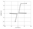
- FIG. 9 is a graph showing current-voltage characteristics of a reverse current blocking diode according to a comparative example.
- FIG. 10 is a graph showing current-voltage characteristics of the first reverse-blocking diode 13 according to this embodiment.
- the current-voltage characteristics shown in FIGS. 9 and 10 were examined by a known TLP (Transmission Line Pulse) measurement method.
- TLP Transmission Line Pulse
- the vertical axis is current [A] and the horizontal axis is voltage [V].
- a positive current means a forward current IF and a negative current means a reverse current IR.
- a positive voltage means a forward voltage VF and a negative voltage means a reverse voltage VR.
- the backflow blocking diode according to the comparative example does not include the impurity region 56 . That is, the reverse current blocking diode according to the comparative example has only the diode structure 90 and does not have the thyristor structure 91 .
- the forward current IF leading to electrostatic breakdown was about +5A, while the reverse current IR leading to electrostatic breakdown was about -0.5A.
- the forward current IF leading to electrostatic breakdown was about +25 A, while the reverse current IR leading to electrostatic breakdown was about -24 A.
- the electrostatic surge withstand capability was improved in both the forward direction and the reverse direction compared to the back-blocking diode according to the comparative example.
- the diode structure 90 and the first transistor structure 92 can handle forward overcurrent.
- the thyristor structure 91 can handle the reverse overcurrent.
- the first reverse-blocking diode 13 according to the present embodiment has improved electrostatic surge resistance as compared with the reverse-blocking diode according to the comparative example.
- the electrostatic surge resistance can be improved.
- the improvement in the electrostatic surge resistance on the forward voltage VF (forward current IF) side due to the action of the first transistor structure 92 can be attributed to the reverse voltage VR. This is a unique effect that cannot be achieved with a general thyristor device used as a protection device.
- the impurity region 56 is formed in the surface layer portion of the well region 50 with a space inward from the edge portion of the well region 50 .
- part of the well region 50 intervenes in the region between the impurity region 56 and the semiconductor layer 25 in the lateral direction parallel to the first main surface 21 , and part of the well region 50 allows the first A base resistor for transistor structure 92 is formed. This allows the thyristor structure 91 to operate properly.
- the base of the first transistor structure 92 is the relatively low-resistance drain region 54 . It is shorted to the emitter of transistor structure 92 . Therefore, the operation of the thyristor structure 91 becomes unstable.
- the edge of the impurity region 56 on the side of the base region 40 is formed inside the well region 50 with respect to the edge of the drain region 54 on the side of the base region 40 .
- short-circuiting of the base and emitter of the first transistor structure 92 by the drain region 54 can be appropriately suppressed. Therefore, the thyristor structure 91 can be operated more appropriately.
- punch-through between the drain region 54 and the source region 41 can be suppressed when an overvoltage is applied between the drain region 54 and the source region 41 . Therefore, a decrease in punch-through breakdown voltage can be suppressed.
- the impurity region 56 faces the drain region 54 in the direction perpendicular to the facing direction of the base region 40 and the well region 50 .
- a thyristor structure 91 can be formed on a line connecting base region 40 and impurity region 56 . Accordingly, it is possible to appropriately prevent the operation of the thyristor structure 91 from being hindered by the drain region 54 .
- the semiconductor device 1 also includes a p-type guard region 60 formed in the column region 31 and the well region 50 in the surface layer portion of the first main surface 21 .
- the guard region 60 is fixed at the same potential as the drain region 54 and the like.
- the semiconductor device 1 is electrically connected to the drain connection electrode 83 connected to the drain region 54 and the like on the first main surface 21 and to the guard region 60 on the first main surface 21, A guard connection electrode 84 fixed to the same potential as the drain connection electrode 83 is included.
- a pnp-type (first polarity type) first electrode layer including the p-type base region 40, the n-type semiconductor layer 25 and the p-type column region 31 is provided. 1 parasitic transistor is formed.
- the forward voltage VF of the diode structure 90 is applied to the source connection electrode 82 (gate electrode 73) and the drain connection electrode 83, leak current flows through the column region 31 via the first parasitic transistor.
- the guard region 60 is formed in the region between the column region 31 and the well region 50.
- the region between the column region 31 and the base region 40 is a pnp-type (first layer) including the p-type base region 40, the n-type semiconductor layer 25 and the p-type guard region 60.
- a second parasitic transistor of a polar type is formed.
- Embodiments of the present invention can be implemented in other forms.
- the insulating film 70 is made of a field oxide film.
- the insulating film 70 may be buried in the trench.
- the trench and the insulating film 70 may form an STI (shallow trench isolation) structure.
- first conductivity type is “p-type” and the “second conductivity type” is “n-type”
- second conductivity type may be "p-type”.
- a specific configuration in this case can be obtained by replacing "n-type region” with “p-type region” and "p-type region” with “n-type region” in the above description and accompanying drawings.
- p-type was expressed as “first conductivity type”
- n-type was expressed as “second conductivity type” in order to clarify the order of explanation.
- “p-type” may be expressed as “second conductivity type”
- n-type may be expressed as “first conductivity type”.
- the first reverse current blocking diode 13 (the second reverse current blocking diode 17) is incorporated in the CAN circuit section.
- the first reverse current blocking diode 13 (the second reverse current blocking diode 17) can also be incorporated in circuit sections for various applications other than CAN.
- the first reverse current blocking diode 13 (second reverse current blocking diode 17) is used in the circuit section of an in-vehicle network such as LIN (Local Interconnect Network) and FlexRay, the circuit section of an in-vehicle switch IC, the circuit section of a DC/DC converter, etc. can be incorporated.
- the first reverse current blocking diode 13 (the second reverse current blocking diode 17) may be incorporated in a circuit section for applications other than in-vehicle applications.
- the EIS type diode structure has a structural feature of low electrostatic surge resistance.
- the electrostatic surge tolerance is also called ESD (electro static discharge) tolerance.
- ESD electro static discharge
- a first conductivity type semiconductor layer having a main surface and including a device region, a second conductivity type base region formed in a surface layer portion of the main surface in the device region, and an edge of the base region a source region of a first conductivity type formed in a surface layer portion of the base region spaced inwardly from the base region and defining a channel region between itself and the semiconductor layer; and the source region in the surface layer portion of the base region.
- a base contact region of a second conductivity type formed in a region different from the base region and having an impurity concentration higher than that of the base region; a first conductivity type well region defining a drift region between itself and the base region; a first conductivity type drain region formed in a surface layer of the well region; and a first conductivity type drain region formed in a surface layer of the well region.
- an impurity region of a second conductivity type electrically connected to the drain region; a gate insulating film covering the channel region on the main surface; and a gate insulating film covering the channel region on the gate insulating film. and a gate structure having gate electrodes facing each other and electrically connected to the source region and the base contact region.
- This semiconductor device includes an EIS type diode structure in the device region.
- a diode structure specifically includes a base region, a source region, a base contact region, a well region, a drain region and a gate structure.
- the semiconductor device also includes a thyristor structure electrically connected to the diode structure in the device region.
- the thyristor structure includes an impurity region (second conductivity type), a semiconductor layer (first conductivity type), a base region (second conductivity type), and a source region formed in this order along the main surface of a semiconductor layer. It includes a region (first conductivity type).
- the thyristor structure includes a first polarity type first transistor structure on the well region side and a second polarity type second transistor structure on the base region side.
- the first transistor structure includes an impurity region (second conductivity type), a semiconductor layer (first conductivity type) and a base region (second conductivity type) formed in this order along the main surface of the semiconductor layer.
- the second transistor structure includes a source region (first conductivity type), a base region (second conductivity type) and a semiconductor layer (first conductivity type) formed in this order along the main surface of the semiconductor layer.
- the diode structure When a forward voltage is applied to the diode structure, the diode structure is turned on while the thyristor structure is turned off. The thyristor structure is turned off because the drain region and the impurity region are fixed at the same potential. This causes the diode structure to conduct and forward current to flow through the diode structure. This forward voltage also flows through the first transistor structure electrically connected to the diode structure. Therefore, when a forward overvoltage, such as due to static electricity, is applied to the diode structure, the forward overcurrent can be handled by the diode structure and the first transistor structure.
- the thyristor structure when a reverse voltage is applied to the diode structure, the thyristor structure is turned on while the diode structure is turned off. This causes the thyristor structure to conduct and reverse current to flow through the thyristor structure.
- a reverse overvoltage such as due to static electricity
- the thyristor structure can handle the reverse overcurrent. Therefore, according to this semiconductor device, the electrostatic surge resistance can be improved.
- A3 The semiconductor device according to A1 or A2, wherein the impurity region is connected to the drain region in a direction perpendicular to the facing direction of the base region and the well region.
- A4 The semiconductor device according to any one of A1 to A3, wherein a plurality of impurity regions are formed to sandwich one drain region.
- the base region is formed in a band shape extending along one direction in a plan view, and the impurity region is formed in a region of the well region facing the long side of the base region, A1 to A5
- the semiconductor device according to any one of .
- the well region is formed in a ring shape surrounding the base region in plan view
- the gate electrode is formed in a ring shape surrounding the base region in a region between the base region and the well region in plan view.
- A8 The semiconductor device according to any one of A1 to A7, further including a region isolation structure formed on the main surface and electrically isolating the device region from other regions.
- A10 further including a second conductivity type guard region formed in a region between the well region and the column region in the surface layer portion of the main surface and electrically connected to the drain region. semiconductor device.
- A11 Any one of A1 to A10, wherein the base contact region is formed in a surface layer portion of the base region spaced inwardly from an edge of the base region and electrically connected to the source region. 1.
- A12 Further including an insulating film covering the drift region on the main surface, wherein the gate insulating film has a thickness less than the thickness of the insulating film and is continuous with the insulating film, A1 The semiconductor device according to any one of A11.
- A14 The semiconductor device according to any one of A1 to A13, further including a semiconductor substrate of a second conductivity type, wherein the semiconductor layer is laminated on the semiconductor substrate.
- the device region further includes a buried region of the first conductivity type formed across a boundary between the semiconductor substrate and the semiconductor layer, wherein the base region and the well region are located on one side of the semiconductor layer.
- A16 The semiconductor device according to A15, further including a channel stop region of the first conductivity type formed in the semiconductor layer along the periphery of the device region in the device region.
- FIG. 11 is a circuit diagram showing the electrical structure of the main part of the semiconductor device 1 according to the second embodiment of the invention.
- the semiconductor device 1 of this embodiment is based on the above-described first embodiment (FIG. 1) and further includes a first electrostatic protection circuit 110 and a second electrostatic protection circuit 120 .
- the actual CAN transceiver IC has, as shown in this figure, the high-side terminal CANH, the low-side terminal CANL, and the ground terminal GND. are provided with a first electrostatic protection circuit 110 and a second electrostatic protection circuit 120, respectively.
- FIG. 12 is a diagram showing an example of the first electrostatic protection circuit 110 and the second electrostatic protection circuit 120 according to the second embodiment.
- the first electrostatic protection circuit 110 and the second electrostatic protection circuit 120 include three first electrostatic protection diodes M11, three second electrostatic protection diodes M12, and five and a third electrostatic protection diode M13.
- the first electrostatic protection circuit 110 is composed of three first electrostatic protection diodes M11 and five third electrostatic protection diodes M13.
- the second electrostatic protection circuit 120 is composed of three second electrostatic protection diodes M12 and five third electrostatic protection diodes M13. That is, the five third electrostatic protection diodes M13 are shared by both the first electrostatic protection circuit 110 and the second electrostatic protection circuit 120.
- the first electrostatic protection diode M11 and the second electrostatic protection diode M12 have long sides in the vertical direction of the paper and short sides in the horizontal direction of the paper when the semiconductor device 1 is viewed from above. It is formed in a rectangular shape.
- the first electrostatic protection diode M11 and the second electrostatic protection diode M12 are arranged in a row along the left-right direction of the paper surface. Referring to this figure, three first electrostatic protection diodes M11 and three second electrostatic protection diodes M12 are arranged adjacent to each other from left to right in the drawing.
- the third electrostatic protection diode M13 is formed in a rectangular shape with short sides extending in the vertical direction of the paper and long sides extending in the horizontal direction of the paper.
- the third electrostatic protection diodes M13 are arranged in a line along the vertical direction of the paper.
- the upper side of the third electrostatic protection diode M13 which is positioned on the uppermost side of the paper surface, is at least part of the first electrostatic protection diode M11 and the second electrostatic protection diode M12. is arranged so as to be adjacent to the lower side of the
- FIG. 14 is a diagram showing current-voltage characteristics of the first electrostatic protection circuit 110 and the second electrostatic protection circuit 120 according to the second embodiment.
- the vertical axis indicates current [A]
- the horizontal axis indicates voltage [V].
- the current-voltage characteristics in this figure are measurement results obtained by a known TLP measurement method.
- the electrostatic surge can be relieved by passing a current through the first electrostatic protection circuit 110 and the second electrostatic protection circuit 120 . Therefore, the safety of the semiconductor device 1 can be ensured.
- the rated voltage for example, -27 V to +40 V
- the third electrostatic protection diode M13 is shared by the first electrostatic protection circuit 110 and the second electrostatic protection circuit 120, as described above. Therefore, the number of the third electrostatic protection diodes M13 can be halved compared to the configuration in which the third electrostatic protection diodes M13 are individually provided for each of the first electrostatic protection circuit 110 and the second electrostatic protection circuit 120. . Therefore, the area of the semiconductor device 1 can be reduced.
- low-voltage NMOS transistors are used as the first electrostatic protection diode M11, the second electrostatic protection diode M12, and the third electrostatic protection diode M13.
- the reason is that the low-voltage NMOS transistor (with a DC voltage of several volts) is more resistant to the instantaneous application of static electricity than the high-voltage NMOS transistor (with a DC voltage of several tens of volts).
- a single low-voltage NMOS transistor cannot withstand the application of the rated DC voltage (eg, -27 V to +40 V) specified for the high-side terminal CANH and low-side terminal CANL. Therefore, in the semiconductor device 1 of the second embodiment, a plurality of low-voltage NMOS transistors must be vertically stacked in order to increase the DC voltage resistance, which may hinder further area saving. 13).
- the rated DC voltage eg, -27 V to +40 V
- FIG. 15 is a diagram showing an example of the first electrostatic protection circuit 110 and the second electrostatic protection circuit 120 according to the third embodiment.
- the first static protection circuit 110 and the second static protection circuit 120 are composed of a first static protection diode M21, a second static protection diode M22, and a third static protection diode M22. and M23.
- the first electrostatic protection diode M21 is connected between the high-side terminal CANH and the internal node n2 with a polarity (corresponding to a first polarity) with the high-side terminal CANH on the anode side and the internal node n2 on the cathode side. ing.
- the anode of the first electrostatic protection diode M21 is connected to the high side terminal CANH.
- the anode of the second electrostatic protection diode M22 is connected to the low side terminal CANL.
- the anode of the third electrostatic protection diode M23 is connected to the ground terminal GND.
- Cathodes of the first electrostatic protection diode M21, the second electrostatic protection diode M22, and the third electrostatic protection diode M23 are all commonly connected to the internal node n2.
- the first electrostatic protection circuit 110 is composed of a first electrostatic protection diode M21 and a third electrostatic protection diode M23.
- the second electrostatic protection circuit 120 is composed of a second electrostatic protection diode M22 and a third electrostatic protection diode M23. That is, the third electrostatic protection diode M23 is shared by both the first electrostatic protection circuit 110 and the second electrostatic protection circuit 120.
- the first electrostatic protection diode M21, the second electrostatic protection diode M22, and the third electrostatic protection diode M23 are not low voltage NMOS transistors, but P-type impurity regions in the drains. and a thyristorized lateral NDMOS transistor.
- the thyristorized lateral NDMOS transistor has the same element structure (see FIGS. 7 and 8) as the first reverse current blocking diode 13 and the second reverse current blocking diode 17 described above. Without repeating the description, briefly restating with reference to FIGS. 7 and 8 , the thyristorized lateral NDMOS transistor includes a thyristor structure 91 electrically connected to a diode structure 90 .
- the semiconductor device 1 (in particular, a thyristorized lateral NDMOS transistor) has a first main surface 21, an n-type semiconductor layer 25 including a device region 26, and a A channel region 42 is defined between a p-type base region 40 formed in the surface layer and a semiconductor layer 25 formed in the surface layer of the base region 40 with a gap inward from the edge of the base region 40 .
- a p-type base contact region 43 formed in a region different from the source region 41 in the surface layer portion of the base region 40 and having an impurity concentration exceeding that of the base region 40; and a device region.
- an n-type well region 50 formed on the surface layer of the first main surface 21 at 26 at a distance from the base region 40 and defining a drift region between the base region 40 and the well region 50; a p-type impurity region 56 formed in the surface layer of the well region 50 and electrically connected to the drain region 54; and the channel region 42 on the first main surface 21. and a gate structure 71 having a gate electrode 73 overlying the gate insulating film 72 and facing the channel region 42 and electrically connected to the source region 41 and the base contact region 43 . .
- a thyristorized lateral NDMOS transistor not only exhibits high electrostatic surge resistance, but also has a very high DC withstand voltage (eg, -40V to +40V). Therefore, even a single element can withstand the application of a rated DC voltage (for example, -27V to +40V) specified for each of the high side terminal CANH and the low side terminal CANL. Therefore, in the semiconductor device 1 of the third embodiment, unlike the second embodiment, it is not necessary to increase the DC withstand voltage by stacking a plurality of low-voltage NMOS transistors in tandem, so that the area can be further reduced. becomes possible.
- the first electrostatic protection diode M21, the second electrostatic protection diode M22, and the third electrostatic protection diode M23 each have a rectangular shape (substantially a square shape) in plan view of the semiconductor device 1. formed.
- the first electrostatic protection diode M21 and the second electrostatic protection diode M22 have a common side (in this figure, the right side of the first electrostatic protection diode and the left side of the second electrostatic protection diode correspond to this). They are arranged adjacent to each other in the left-right direction of the paper surface so as to hold.
- the third electrostatic protection diode M23 is arranged adjacent to the first electrostatic protection diode M21 and the second electrostatic protection diode M22 in the vertical direction of the paper surface.
- the third electrostatic protection diode M23 is arranged so that its upper side is evenly in contact with the lower sides of the first electrostatic protection diode M21 and the second electrostatic protection diode M22. That is, the common side of the first electrostatic protection diode M21 and the second electrostatic protection diode M22 corresponds to a perpendicular line that bisects the upper side of the third electrostatic protection diode M23.
- FIG. 17 is a diagram showing current-voltage characteristics of the first electrostatic protection circuit 110 and the second electrostatic protection circuit 120 according to the third embodiment.
- the vertical axis in this figure indicates the current [A]
- the horizontal axis indicates the voltage [V].
- the current-voltage characteristics in this figure are measurement results obtained by a known TLP measurement method.
- the semiconductor device 1 of the third embodiment can withstand application of a high DC voltage (eg, -40 V to +40 V) without cascading a plurality of transistor elements. Therefore, it is possible to achieve both high DC withstand voltage, high ESD withstand voltage, and area saving.
- a high DC voltage eg, -40 V to +40 V
- FIG. 18 is a diagram showing an example of the second electrostatic protection circuit 120 (and its peripheral circuits) according to the fourth embodiment.
- the low-side output circuit 4 may also use the second electrostatic protection diode M22 as the second reverse-blocking diode 17 that blocks reverse current from the ground terminal GND to the low-side terminal CANL.
- the third electrostatic protection diode M23 forming the second electrostatic protection circuit 120 is connected in parallel to the second drive transistor 15 and the second protection transistor 16 included in the low-side output circuit 4. Become.
- the semiconductor device disclosed in this specification has a configuration (first configuration) that includes a lateral NDMOS transistor that is formed into a thyristor by forming a P-type impurity region in the drain as an electrostatic protection diode.
- the semiconductor device disclosed in this specification includes a first signal terminal, a second signal terminal, a ground terminal, a first electrostatic protection diode, a second electrostatic protection diode, and a third electrostatic protection diode. and an electrostatic protection diode, wherein each of the first electrostatic protection diode, the second electrostatic protection diode, and the third electrostatic protection diode is a lateral thyristor formed by forming a P-type impurity region in the drain.
- an NDMOS transistor wherein the anode of the first static protection diode is connected to the first signal terminal, the anode of the second static protection diode is connected to the second signal terminal, and the third static protection diode is connected to the ground terminal, and the cathodes of the first electrostatic protection diode, the second electrostatic protection diode, and the third electrostatic protection diode are connected in common (second configuration) It is said that
- the first electrostatic protection diode, the second electrostatic protection diode, and the third electrostatic protection diode are formed in a rectangular shape in a plan view.
- the first electrostatic protection diode and the second electrostatic protection diode are arranged to have a common side, and the third electrostatic protection diode is the first electrostatic protection diode and the second electrostatic protection diode.
- a configuration (third configuration) in which the diodes are evenly in contact with both of the diodes may be employed.
- the semiconductor device is a CAN transceiver
- the first signal terminal is a high-side bus input/output terminal
- the second signal terminal is a low-side bus input/output terminal.
- bus input/output terminals (fourth configuration).
- the semiconductor device includes a high-side output circuit configured to conduct/disconnect between the first signal terminal and the power supply terminal, and a high-side output circuit configured to connect/disconnect the second signal terminal and the ground terminal. and a low-side output circuit configured to conduct/interrupt between them (fifth configuration).
- the high-side output circuit includes a first reverse-blocking diode configured to block reverse current from the first signal terminal to the power supply terminal (sixth configuration). configuration).
- the low-side output circuit includes a second reverse-blocking diode configured to block reverse current from the ground terminal to the second signal terminal (seventh configuration). configuration).
- the low-side output circuit also serves as the second electrostatic protection diode as a second reverse-blocking diode that blocks reverse current from the ground terminal to the second signal terminal. (Eighth configuration).
- the lateral NDMOS transistor has a main surface and includes a first conductivity type semiconductor layer including a device region, and a semiconductor layer of the first conductivity type in the device region.
- a second conductivity type base region formed in a surface layer portion and a channel region formed in a surface layer portion of the base region spaced inwardly from an edge portion of the base region to define a channel region between the semiconductor layer and the base region.
- a second conductivity type base contact region formed in a region different from the source region in a surface layer portion of the base region and having an impurity concentration exceeding the impurity concentration of the base region; a well region of a first conductivity type formed in a surface layer portion of the main surface spaced apart from the base region in the device region and defining a drift region between the base region and the well region; a drain region of a first conductivity type formed; an impurity region of a second conductivity type formed in a surface layer portion of the well region and electrically connected to the drain region; and the channel region on the main surface. and a gate structure having a gate electrode on the gate insulating film facing the channel region and electrically connected to the source region and the base contact region ( 9th configuration).
- the semiconductor device disclosed in this specification includes a first signal terminal, a second signal terminal, a ground terminal, and a signal connected between the first signal terminal and an internal node with a first polarity. and at least one second electrostatic protection diode configured to be connected in the first polarity between the second signal terminal and the internal node. an electrostatic protection diode; and at least one third electrostatic protection diode configured to be connected between the internal node and the ground terminal with a second polarity opposite to the first polarity. configuration (tenth configuration).
Landscapes
- Metal-Oxide And Bipolar Metal-Oxide Semiconductor Integrated Circuits (AREA)
- Semiconductor Integrated Circuits (AREA)
Priority Applications (4)
| Application Number | Priority Date | Filing Date | Title |
|---|---|---|---|
| DE112022005497.2T DE112022005497T5 (de) | 2021-11-18 | 2022-10-04 | Halbleiterbauteil |
| JP2023561442A JPWO2023089974A1 (https=) | 2021-11-18 | 2022-10-04 | |
| CN202280074679.1A CN118235247A (zh) | 2021-11-18 | 2022-10-04 | 半导体装置 |
| US18/656,653 US20240290778A1 (en) | 2021-11-18 | 2024-05-07 | Semiconductor device |
Applications Claiming Priority (2)
| Application Number | Priority Date | Filing Date | Title |
|---|---|---|---|
| JP2021-187649 | 2021-11-18 | ||
| JP2021187649 | 2021-11-18 |
Related Child Applications (1)
| Application Number | Title | Priority Date | Filing Date |
|---|---|---|---|
| US18/656,653 Continuation US20240290778A1 (en) | 2021-11-18 | 2024-05-07 | Semiconductor device |
Publications (1)
| Publication Number | Publication Date |
|---|---|
| WO2023089974A1 true WO2023089974A1 (ja) | 2023-05-25 |
Family
ID=86396706
Family Applications (1)
| Application Number | Title | Priority Date | Filing Date |
|---|---|---|---|
| PCT/JP2022/037107 Ceased WO2023089974A1 (ja) | 2021-11-18 | 2022-10-04 | 半導体装置 |
Country Status (5)
| Country | Link |
|---|---|
| US (1) | US20240290778A1 (https=) |
| JP (1) | JPWO2023089974A1 (https=) |
| CN (1) | CN118235247A (https=) |
| DE (1) | DE112022005497T5 (https=) |
| WO (1) | WO2023089974A1 (https=) |
Families Citing this family (1)
| Publication number | Priority date | Publication date | Assignee | Title |
|---|---|---|---|---|
| US20230378165A1 (en) * | 2022-05-23 | 2023-11-23 | CoolStar Technology, Inc. | Electrostatic Discharge Protection Device Having Multiple Pairs of PN Stripes and Methods of Fabrication Thereof |
Citations (2)
| Publication number | Priority date | Publication date | Assignee | Title |
|---|---|---|---|---|
| JP2017054864A (ja) * | 2015-09-07 | 2017-03-16 | アルプス電気株式会社 | Esd保護回路及び半導体集積回路装置 |
| WO2021106939A1 (ja) * | 2019-11-29 | 2021-06-03 | ローム株式会社 | 半導体装置 |
Family Cites Families (2)
| Publication number | Priority date | Publication date | Assignee | Title |
|---|---|---|---|---|
| JP4701886B2 (ja) | 2005-07-13 | 2011-06-15 | 富士電機システムズ株式会社 | 半導体装置 |
| JP6674113B2 (ja) | 2018-06-21 | 2020-04-01 | サミー株式会社 | 遊技機 |
-
2022
- 2022-10-04 WO PCT/JP2022/037107 patent/WO2023089974A1/ja not_active Ceased
- 2022-10-04 JP JP2023561442A patent/JPWO2023089974A1/ja active Pending
- 2022-10-04 CN CN202280074679.1A patent/CN118235247A/zh active Pending
- 2022-10-04 DE DE112022005497.2T patent/DE112022005497T5/de active Pending
-
2024
- 2024-05-07 US US18/656,653 patent/US20240290778A1/en active Pending
Patent Citations (2)
| Publication number | Priority date | Publication date | Assignee | Title |
|---|---|---|---|---|
| JP2017054864A (ja) * | 2015-09-07 | 2017-03-16 | アルプス電気株式会社 | Esd保護回路及び半導体集積回路装置 |
| WO2021106939A1 (ja) * | 2019-11-29 | 2021-06-03 | ローム株式会社 | 半導体装置 |
Also Published As
| Publication number | Publication date |
|---|---|
| CN118235247A (zh) | 2024-06-21 |
| US20240290778A1 (en) | 2024-08-29 |
| JPWO2023089974A1 (https=) | 2023-05-25 |
| DE112022005497T5 (de) | 2024-09-05 |
Similar Documents
| Publication | Publication Date | Title |
|---|---|---|
| JP6337634B2 (ja) | 半導体集積回路装置 | |
| CN116207095B (zh) | 瞬态电压抑制装置 | |
| JP5801609B2 (ja) | 保護回路素子 | |
| US20080013231A1 (en) | Esd protection circuit | |
| TW202017143A (zh) | 低電容瞬態電壓抑制器 | |
| US20250107116A1 (en) | Semiconductor device | |
| TWI625840B (zh) | 靜電放電保護裝置 | |
| KR100311578B1 (ko) | 반도체장치 | |
| US9711592B2 (en) | Diode and signal output circuit including the same | |
| US20120098046A1 (en) | Electrostatic discharge protection device | |
| CN104852572A (zh) | 高耐压集成电路装置 | |
| CN106960841B (zh) | 高压晶体管 | |
| JP2007335440A (ja) | 半導体装置の静電破壊保護方法及び静電破壊保護装置 | |
| US8878284B2 (en) | Programmable SCR for LDMOS ESD protection | |
| JP5243773B2 (ja) | 静電気保護用半導体装置 | |
| WO2023089974A1 (ja) | 半導体装置 | |
| JP2010129663A (ja) | 半導体装置 | |
| JP4423466B2 (ja) | 半導体装置 | |
| JP2025143689A (ja) | 半導体装置 | |
| KR101442252B1 (ko) | 반도체 장치 | |
| KR20190068400A (ko) | 다이오드를 내장한 mos 구조의 사이리스터 소자 | |
| JP2009038101A (ja) | 半導体装置 | |
| JP2025022576A (ja) | 半導体装置 | |
| JPH0917953A (ja) | 半導体装置の保護装置 |
Legal Events
| Date | Code | Title | Description |
|---|---|---|---|
| 121 | Ep: the epo has been informed by wipo that ep was designated in this application |
Ref document number: 22895260 Country of ref document: EP Kind code of ref document: A1 |
|
| ENP | Entry into the national phase |
Ref document number: 2023561442 Country of ref document: JP Kind code of ref document: A |
|
| WWE | Wipo information: entry into national phase |
Ref document number: 202280074679.1 Country of ref document: CN |
|
| WWE | Wipo information: entry into national phase |
Ref document number: 112022005497 Country of ref document: DE |
|
| 122 | Ep: pct application non-entry in european phase |
Ref document number: 22895260 Country of ref document: EP Kind code of ref document: A1 |