WO2023085210A1 - Dispositif à ondes élastiques, filtre, diviseur, et dispositif de communication - Google Patents
Dispositif à ondes élastiques, filtre, diviseur, et dispositif de communication Download PDFInfo
- Publication number
- WO2023085210A1 WO2023085210A1 PCT/JP2022/041167 JP2022041167W WO2023085210A1 WO 2023085210 A1 WO2023085210 A1 WO 2023085210A1 JP 2022041167 W JP2022041167 W JP 2022041167W WO 2023085210 A1 WO2023085210 A1 WO 2023085210A1
- Authority
- WO
- WIPO (PCT)
- Prior art keywords
- layer
- piezoelectric film
- values
- thickness
- elastic wave
- Prior art date
Links
- 238000004891 communication Methods 0.000 title claims description 12
- 239000000463 material Substances 0.000 claims abstract description 79
- 239000013078 crystal Substances 0.000 claims abstract description 33
- 235000019687 Lamb Nutrition 0.000 claims abstract description 26
- WSMQKESQZFQMFW-UHFFFAOYSA-N 5-methyl-pyrazole-3-carboxylic acid Chemical group CC1=CC(C(O)=O)=NN1 WSMQKESQZFQMFW-UHFFFAOYSA-N 0.000 claims description 11
- GQYHUHYESMUTHG-UHFFFAOYSA-N lithium niobate Chemical group [Li+].[O-][Nb](=O)=O GQYHUHYESMUTHG-UHFFFAOYSA-N 0.000 claims description 11
- 230000001902 propagating effect Effects 0.000 claims description 10
- VYPSYNLAJGMNEJ-UHFFFAOYSA-N Silicium dioxide Chemical group O=[Si]=O VYPSYNLAJGMNEJ-UHFFFAOYSA-N 0.000 claims description 8
- 238000010030 laminating Methods 0.000 claims description 8
- 235000012239 silicon dioxide Nutrition 0.000 claims description 4
- 239000000377 silicon dioxide Substances 0.000 claims description 4
- 229910000449 hafnium oxide Inorganic materials 0.000 claims 1
- WIHZLLGSGQNAGK-UHFFFAOYSA-N hafnium(4+);oxygen(2-) Chemical group [O-2].[O-2].[Hf+4] WIHZLLGSGQNAGK-UHFFFAOYSA-N 0.000 claims 1
- 238000010586 diagram Methods 0.000 description 26
- 239000011295 pitch Substances 0.000 description 25
- 238000004088 simulation Methods 0.000 description 25
- 230000000704 physical effect Effects 0.000 description 24
- 230000005540 biological transmission Effects 0.000 description 21
- 239000000758 substrate Substances 0.000 description 21
- 230000014509 gene expression Effects 0.000 description 9
- 230000000694 effects Effects 0.000 description 6
- 229910004298 SiO 2 Inorganic materials 0.000 description 4
- MCMNRKCIXSYSNV-UHFFFAOYSA-N ZrO2 Inorganic materials O=[Zr]=O MCMNRKCIXSYSNV-UHFFFAOYSA-N 0.000 description 4
- 238000004364 calculation method Methods 0.000 description 4
- 238000009795 derivation Methods 0.000 description 4
- 238000011156 evaluation Methods 0.000 description 4
- 239000000395 magnesium oxide Substances 0.000 description 4
- CPLXHLVBOLITMK-UHFFFAOYSA-N magnesium oxide Inorganic materials [Mg]=O CPLXHLVBOLITMK-UHFFFAOYSA-N 0.000 description 4
- AXZKOIWUVFPNLO-UHFFFAOYSA-N magnesium;oxygen(2-) Chemical compound [O-2].[Mg+2] AXZKOIWUVFPNLO-UHFFFAOYSA-N 0.000 description 4
- 229910052751 metal Inorganic materials 0.000 description 4
- 239000002184 metal Substances 0.000 description 4
- 229910000838 Al alloy Inorganic materials 0.000 description 3
- 230000001681 protective effect Effects 0.000 description 3
- PBCFLUZVCVVTBY-UHFFFAOYSA-N tantalum pentoxide Inorganic materials O=[Ta](=O)O[Ta](=O)=O PBCFLUZVCVVTBY-UHFFFAOYSA-N 0.000 description 3
- 239000010936 titanium Substances 0.000 description 3
- GWEVSGVZZGPLCZ-UHFFFAOYSA-N Titan oxide Chemical compound O=[Ti]=O GWEVSGVZZGPLCZ-UHFFFAOYSA-N 0.000 description 2
- 229910045601 alloy Inorganic materials 0.000 description 2
- 239000000956 alloy Substances 0.000 description 2
- 238000006243 chemical reaction Methods 0.000 description 2
- 238000006073 displacement reaction Methods 0.000 description 2
- CJNBYAVZURUTKZ-UHFFFAOYSA-N hafnium(iv) oxide Chemical compound O=[Hf]=O CJNBYAVZURUTKZ-UHFFFAOYSA-N 0.000 description 2
- 230000012447 hatching Effects 0.000 description 2
- 238000003475 lamination Methods 0.000 description 2
- BPUBBGLMJRNUCC-UHFFFAOYSA-N oxygen(2-);tantalum(5+) Chemical group [O-2].[O-2].[O-2].[O-2].[O-2].[Ta+5].[Ta+5] BPUBBGLMJRNUCC-UHFFFAOYSA-N 0.000 description 2
- RVTZCBVAJQQJTK-UHFFFAOYSA-N oxygen(2-);zirconium(4+) Chemical compound [O-2].[O-2].[Zr+4] RVTZCBVAJQQJTK-UHFFFAOYSA-N 0.000 description 2
- 230000005236 sound signal Effects 0.000 description 2
- 238000010897 surface acoustic wave method Methods 0.000 description 2
- 229910013641 LiNbO 3 Inorganic materials 0.000 description 1
- RTAQQCXQSZGOHL-UHFFFAOYSA-N Titanium Chemical compound [Ti] RTAQQCXQSZGOHL-UHFFFAOYSA-N 0.000 description 1
- 229910052782 aluminium Inorganic materials 0.000 description 1
- XAGFODPZIPBFFR-UHFFFAOYSA-N aluminium Chemical compound [Al] XAGFODPZIPBFFR-UHFFFAOYSA-N 0.000 description 1
- WPPDFTBPZNZZRP-UHFFFAOYSA-N aluminum copper Chemical compound [Al].[Cu] WPPDFTBPZNZZRP-UHFFFAOYSA-N 0.000 description 1
- 238000013459 approach Methods 0.000 description 1
- 239000000919 ceramic Substances 0.000 description 1
- 229910052681 coesite Inorganic materials 0.000 description 1
- 239000010949 copper Substances 0.000 description 1
- 230000002596 correlated effect Effects 0.000 description 1
- 230000000875 corresponding effect Effects 0.000 description 1
- 238000005260 corrosion Methods 0.000 description 1
- 230000007797 corrosion Effects 0.000 description 1
- 229910052906 cristobalite Inorganic materials 0.000 description 1
- 238000009792 diffusion process Methods 0.000 description 1
- 238000001914 filtration Methods 0.000 description 1
- 239000012212 insulator Substances 0.000 description 1
- 238000005259 measurement Methods 0.000 description 1
- 238000000034 method Methods 0.000 description 1
- TWNQGVIAIRXVLR-UHFFFAOYSA-N oxo(oxoalumanyloxy)alumane Chemical compound O=[Al]O[Al]=O TWNQGVIAIRXVLR-UHFFFAOYSA-N 0.000 description 1
- 230000003014 reinforcing effect Effects 0.000 description 1
- 239000011347 resin Substances 0.000 description 1
- 229920005989 resin Polymers 0.000 description 1
- 229910052594 sapphire Inorganic materials 0.000 description 1
- 239000010980 sapphire Substances 0.000 description 1
- 239000004065 semiconductor Substances 0.000 description 1
- 229910052710 silicon Inorganic materials 0.000 description 1
- 239000010703 silicon Substances 0.000 description 1
- 229910052682 stishovite Inorganic materials 0.000 description 1
- 229910052719 titanium Inorganic materials 0.000 description 1
- 229910052905 tridymite Inorganic materials 0.000 description 1
Images


Classifications
-
- H—ELECTRICITY
- H03—ELECTRONIC CIRCUITRY
- H03H—IMPEDANCE NETWORKS, e.g. RESONANT CIRCUITS; RESONATORS
- H03H9/00—Networks comprising electromechanical or electro-acoustic devices; Electromechanical resonators
- H03H9/25—Constructional features of resonators using surface acoustic waves
-
- H—ELECTRICITY
- H03—ELECTRONIC CIRCUITRY
- H03H—IMPEDANCE NETWORKS, e.g. RESONANT CIRCUITS; RESONATORS
- H03H9/00—Networks comprising electromechanical or electro-acoustic devices; Electromechanical resonators
- H03H9/46—Filters
- H03H9/64—Filters using surface acoustic waves
-
- H—ELECTRICITY
- H03—ELECTRONIC CIRCUITRY
- H03H—IMPEDANCE NETWORKS, e.g. RESONANT CIRCUITS; RESONATORS
- H03H9/00—Networks comprising electromechanical or electro-acoustic devices; Electromechanical resonators
- H03H9/70—Multiple-port networks for connecting several sources or loads, working on different frequencies or frequency bands, to a common load or source
- H03H9/72—Networks using surface acoustic waves
Definitions
- the present disclosure relates to an elastic wave device that uses elastic waves, and a filter, branching filter, and communication device that have the elastic wave device.
- An elastic wave device that applies a voltage to IDT (interdigital transducer) electrodes on a piezoelectric body to generate an elastic wave that propagates through the piezoelectric body.
- IDT interdigital transducer
- a device in which a piezoelectric body (piezoelectric film) is arranged on a multilayer film is known (for example, Patent Documents 1 and 2).
- the multilayer film is constructed, for example, by alternately laminating first layers and second layers having an acoustic impedance higher than that of the first layers.
- the piezoelectric material is, for example, a single crystal of lithium tantalate (LiTaO 3 , hereinafter sometimes referred to as “LT”) or lithium niobate (LiNbO 3 , hereinafter sometimes referred to as “LN”). Single crystal.
- LT lithium tantalate
- LN lithium niobate
- Patent Document 1 discloses silicon dioxide (SiO 2 ) as the material of the first layer. Further, Patent Document 1 discloses that the material of the second layer is tantalum pentoxide (Ta 2 O 5 ), hafnium oxide (HfO 2 ), zirconium dioxide (ZrO 2 ), titanium dioxide (TiO 2 ) or magnesium oxide (MgO). is disclosed. Patent Literature 1 discloses examples of thicknesses of the first layer and the second layer when the material of the first layer and the material of the second layer are any of the materials described above.
- An acoustic wave device includes a multilayer film, a piezoelectric film positioned on the multilayer film and propagating a Lamb wave in A1 mode, and a piezoelectric film positioned on the piezoelectric film, the Lamb wave and an IDT electrode for exciting waves.
- the multilayer film is configured by alternately laminating first layers and second layers having an acoustic impedance higher than that of the first layers.
- the normalized thickness of the first layer is x
- the normalized thickness of the second layer is y.
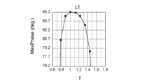
- the material of the piezoelectric film is lithium tantalate single crystal, and the values of x and y are located in the range where MaxPhase is 82.2° or more in FIG.
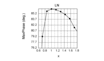
- the material of the piezoelectric film is lithium niobate single crystal, and the values of x and y are located in the range where MaxPhase is 83.4° or more in FIG.
- t L ′ thickness of the first layer ( ⁇ m)
- t H thickness of the second layer ( ⁇ m)
- tL and tH are obtained by the following equations.
- t L ⁇ ( ⁇ 6.88 ⁇ 10 ⁇ 7 E L 2 +6.02 ⁇ 10 ⁇ 5 E L ⁇ 3.7 ⁇ 10 ⁇ 3 )Z H + (2.71 ⁇ 10 ⁇ 5 E L 2 +3.76 ⁇ 10 ⁇ 4 E L +1.78 ⁇ 10 ⁇ 1 ) ⁇ ⁇ 5250/fr
- t H (5.12 ⁇ 10 ⁇ 7 V H ⁇ 4.03 ⁇ 10 ⁇ 2 ) ⁇ 5250/fr
- a filter according to one aspect of the present disclosure includes the above elastic wave device.
- a duplexer includes the filter, another filter, and an antenna terminal to which the filter and the another filter are connected together.
- a communication device includes the branching filter, the antenna connected to the antenna terminal, and the transmitting filter and the receiving filter connected on the opposite side of the antenna terminal with respect to a signal path. and an integrated circuit element comprising:
- FIG. 4 is a contour map showing the relationship between the thickness of the first layer and the thickness of the second layer and the characteristics of the elastic wave device when the material of the piezoelectric film is LT.
- FIG. 4 is a contour diagram showing the relationship between the thickness of the first layer and the thickness of the second layer and the characteristics of the elastic wave device when the material of the piezoelectric film is LN.
- FIG. 2 is a schematic plan view showing the configuration of an elastic wave device; Sectional drawing in the II-II line of FIG.
- FIG. 4 is a diagram showing an example of absolute values of impedance in a resonator;
- FIG. 4 is a diagram showing an example of impedance phases in a resonator;
- FIG. 4 is a diagram showing the dependence of the reference thickness of the first layer on the physical property values of the multilayer film when the material of the piezoelectric film is LT.
- FIG. 8 is a diagram showing the correlation between the slope of the approximate straight line shown in FIG. 7 and the Young's modulus of the first layer;
- FIG. 8 is a diagram showing the correlation between the intercept of the approximate straight line shown in FIG. 7 and the Young's modulus of the first layer;
- FIG. 4 is a diagram showing the dependence of the reference thickness of the second layer on the physical property values of the multilayer film when the material of the piezoelectric film is LT.
- FIG. 4 is a diagram showing the dependence of the reference thickness of the first layer on the physical property values of the multilayer film when the material of the piezoelectric film is LN.
- FIG. 15 is a diagram showing the correlation between the slope of the approximate straight line shown in FIG. 14 and the Young's modulus of the first layer;
- FIG. 15 is a diagram showing the correlation between the intercept of the approximate straight line shown in FIG. 14 and the Young's modulus of the first layer;
- FIG. 4 is a diagram showing the dependence of the reference thickness of the second layer on the physical property values of the multilayer film when the material of the piezoelectric film is LN. The figure which added various information to FIG.
- FIG. 2 is a circuit diagram schematically showing the configuration of a branching filter as an application example of the elastic wave device of FIG. 1;
- FIG. 2 is a circuit diagram schematically showing the configuration of a communication device as an application example of the elastic wave device of FIG. 1;
- x standardized thickness of the first layer 11 y: standardized thickness of the second layer 13 tL ': thickness of the first layer 11 ( ⁇ m) tH ': thickness of the second layer 13 ( ⁇ m) t L ′′: Reference thickness of the first layer 11 ( ⁇ m) t H ′′: Reference thickness of the second layer 13 ( ⁇ m) t L : reference thickness of the first layer 11 ( ⁇ m) t H : reference thickness of the second layer 13 ( ⁇ m) E L : Young's modulus (GPa) of the first layer 11 Z H : Acoustic impedance of the second layer 13 (MRayl) fr: resonance frequency of resonator 15 (MHz) V H : Velocity of sound in the second layer 13 (m/sec)
- the electrical impedance may be simply referred to as impedance for convenience.
- FIG. 3 is a plan view showing the configuration of the main part of the elastic wave device 1 according to this embodiment.
- FIG. 4 is a cross-sectional view taken along line IV--IV of FIG.
- the elastic wave device 1 may be oriented either upward or downward. Terms such as the upper surface or the lower surface may be used, with the positive side of .
- the term "planar view” or “planar see-through” refers to viewing in the D3 direction.
- the D1 axis is defined to be parallel to the propagation direction of an elastic wave propagating along the upper surface of the piezoelectric film 7, which will be described later, and the D2 axis is defined to be parallel to the upper surface of the piezoelectric film 7 and perpendicular to the D1 axis.
- the D3 axis is defined to be orthogonal to the upper surface of the piezoelectric film 7 .
- the acoustic wave device 1 includes, for example, a substrate 3 (FIG. 4), a multilayer film 5 (FIG. 4) positioned on the substrate 3, a piezoelectric film 7 positioned on the multilayer film 5, and a piezoelectric film 7 positioned on the piezoelectric film 7. and a conductive layer 9 .
- the acoustic impedance of the first layer 11 is lower than the acoustic impedance of the second layer 13 .
- the acoustic wave device 1 has a resonator 15 (reference numeral is shown in FIG. 3) made up of these layers.
- the multilayer film 5 is formed by alternately laminating first layers 11 and second layers 13 having different acoustic impedances.
- An electrical signal flowing through the conductive layer 9 is converted into an elastic wave propagating through the piezoelectric film 7 .
- the elastic wave propagating through the piezoelectric film 7 is converted into an electrical signal flowing through the conductive layer 9 .
- Resonance and/or filtering of electrical signals is then achieved, for example, using resonance of acoustic waves.
- the multilayer film 5 contributes to, for example, reflecting elastic waves and confining the energy of the elastic waves in the piezoelectric film 7 .
- the substrate 3 contributes to reinforcing the strength of the multilayer film 5 and the piezoelectric film 7, for example.
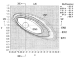
- FIG. 1 and 2 are contour diagrams showing the characteristics of the resonator 15.
- FIG. FIG. 1 shows the case where the material of the piezoelectric film 7 is LT single crystal.
- FIG. 2 shows the case where the material of the piezoelectric film 7 is LN single crystal.
- the horizontal axis x is the normalized thickness of the first layer 11.
- the vertical axis y is the normalized thickness of the second layer 13 .
- MaxPhase (deg.), whose magnitude is indicated by contour lines, indicates the characteristics of the resonator 15, as will be described later. The larger the MaxPhase, the better the characteristics.
- the values of the normalized thickness x and the normalized thickness y in FIG. 1 or 2 are set to fall within a predetermined range.
- the values of x and y are set so that MaxPhase is 82.2° or more in FIG.
- the values of x and y are set so that MaxPhase is 83.4° or more in FIG.
- MaxPhase need not be 82.2° or more. That is, "the range in which MaxPhase is 82.2° or more in FIG. 1" is merely an expression for indicating the range of x and y in FIG.
- Elastic wave device 1 1.1. Configuration of elastic wave device 1 (FIGS. 3 and 4) 1.2. MaxPhase ( Figures 5 and 6) 1.3. x and y for LT (FIGS. 1 and 7-13) 1.4. x and y for LN (FIGS. 2 and 14-20) 1.5. Summary of elastic wave device 1 2 .
- Duplexer including elastic wave device 1 Fig. 21
- Communication device including elastic wave device 1 FIG. 22
- Elastic wave device (1.1. Configuration of elastic wave device)
- the elastic wave device 1 shown in FIGS. 3 and 4 has a plurality of layers (3, 5, 7 (11 and 13) and 9) laminated one another as described above.
- the combination of the substrate 3, the multilayer film 5 and the piezoelectric film 7 is sometimes referred to as a fixed substrate 2 (reference numeral is shown in FIG. 4).
- Each layer (3, 5, 7, 9, 11 and 13) has a substantially constant thickness. Additional layers may be interposed between overlapping layers to improve bond strength between layers or to reduce diffusion between layers. The thickness of this additional layer is, for example, relatively thin (eg, 0.01 ⁇ or less, ⁇ being discussed below).
- the material and dimensions of the substrate 3 are arbitrary. Since the elastic wave propagating through the piezoelectric film 7 is basically reflected by the multilayer film 5, the direct influence of the material and dimensions of the substrate 3 on the elastic wave propagating through the piezoelectric film 7 is relatively small. None.
- the material of the substrate 3 may have a lower coefficient of thermal expansion than the piezoelectric film 7 or the like. In this case, for example, it is possible to reduce the possibility that the frequency characteristics of the acoustic wave device 1 change due to temperature changes. Examples of such materials include semiconductors such as silicon, single crystals such as sapphire, and ceramics such as aluminum oxide sintered bodies.
- the substrate 3 may be configured by laminating a plurality of layers made of different materials. The thickness of the substrate 3 is, for example, thicker than the piezoelectric film 7 .
- the multilayer film 5 is configured by alternately laminating the first layers 11 and the second layers 13 having different acoustic impedances. Due to the difference in acoustic impedance between the two, the elastic wave reflectance is relatively high at the interface between the two. As a result, for example, leakage of elastic waves propagating through the piezoelectric film 7 is reduced.
- the material of the first layer 11 and the material of the second layer 13 are arbitrary as long as the acoustic impedance of the first layer 11 is lower than the acoustic impedance of the second layer 13. Physical property values (density, Young's modulus, and sound velocity) that affect acoustic impedance may also be set arbitrarily.
- the acoustic impedance of the first layer 11 and the acoustic impedance of the second layer 13 may be larger or smaller than the acoustic impedance of the piezoelectric film 7 .
- the material of the first layer 11 may be silicon dioxide ( SiO2 ).
- the material of the second layer 13 may be tantalum pentoxide ( Ta2O5 ), hafnium oxide ( HfO2 ), zirconium dioxide ( ZrO2 ), titanium oxide ( TiO2 ) or magnesium oxide (MgO).
- the number of layers of the multilayer film 5 may be set appropriately.
- the total lamination number of the first layers 11 and the second layers 13 may be two or more, three or more, six or more, or eight or more. Even if the number of laminated layers is only two, the effect of reflecting elastic waves at the interface between the first layer 11 and the second layer 13 can be obtained. Also, the effect of confining the elastic wave in the piezoelectric film 7 increases as the number of layers increases.
- the upper limit of the number of layers to be laminated is not particularly limited, it may be, for example, 12 layers or less.
- the total lamination number of the multilayer film 5 may be an even number or an odd number.
- the layer in contact with the piezoelectric film 7 may be either the first layer 11 or the second layer 13 .
- the first layer 11 may be in contact with the piezoelectric film 7 .
- the difference between the acoustic impedance of SiO 2 and the acoustic impedance of LT or LN is greater than the difference between the acoustic impedance of the previously exemplified materials of the second layer 13 and the acoustic impedance of LT or LN. Therefore, the first layer 11 is in contact with the piezoelectric film 7, so that the effect of confining the elastic wave in the piezoelectric film 7 is improved.
- the layer in contact with the substrate 3 may be either the first layer 11 or the second layer 13 .
- the material of the piezoelectric film 7 is a single crystal of LT or LN, as described above.
- the cut angle and thickness of the piezoelectric film 7 may be set so that the A1 mode Lamb wave can be used.
- the Lamb wave is a wave whose main components are a displacement component in the propagation direction (D1 direction) and a displacement component in the thickness direction (D3 direction) of the piezoelectric film 7 .
- the A1 mode Lamb wave is a Lamb wave having one node in the thickness direction. Examples of cut angles and thicknesses are shown below.
- the cut angle is, for example, Euler angles ( ⁇ , ⁇ , ⁇ ) (0° ⁇ 20°, ⁇ 5° to 65°, 0° ⁇ 10°). may be assumed.
- LT is for rotational Y-cut X-propagation, and the Y-axis may be tilted at an angle of 85° or more and 155° with respect to the normal to the piezoelectric film 7 (D3 axis).
- the X axis may be substantially parallel to the upper surface (D1 axis) of the piezoelectric film 7 .
- the X-axis and the D1-axis may be inclined at -10° or more and 10° or less on the XZ plane or the D1D2 plane.
- the cut angle may be, for example, Euler angles (0° ⁇ 10°, 0 ⁇ 25°, 0° to 360°). Also, the cut angle may be a cut angle that is equivalent to the above cut angle.
- the thickness of the piezoelectric film 7 is relatively thin, and may be, for example, 0.75 ⁇ or less based on ⁇ , which will be described later. More specifically, for example, it may be 0.15 ⁇ or more and 0.3 ⁇ or less.
- the conductive layer 9 is made of metal, for example.
- the metal may be of any suitable type, such as aluminum (Al) or an alloy based on Al (Al alloy).
- Al alloys are, for example, aluminum-copper (Cu) alloys.
- the conductive layer 9 may be composed of a plurality of metal layers.
- a relatively thin layer of titanium (Ti) may be provided between Al or an Al alloy and the piezoelectric film 7 to strengthen their bondability.
- the thickness of the conductive layer 9 may be appropriately set according to the properties required for the elastic wave device 1 .
- the thickness of the conductive layer 9 may be 0.04p or more and 0.20p or less (p will be described later) and/or 50 nm or more and 600 nm or less.
- the conductive layer 9 includes, for example, an IDT electrode 19 and a pair of reflectors 21 located on both sides of the IDT electrode 19 .
- a resonator 15 is configured by regions of the multilayer film 5, the piezoelectric film 7, and the conductive layer 9 where the IDT electrode 19 and the pair of reflectors 21 are arranged.
- the resonator 15 is configured as a so-called one-port elastic wave resonator, and when an electric signal of a predetermined frequency is input from one of terminals 17A and 17B conceptually and schematically shown, resonance occurs, and the resonance occurs. The resulting signal can be output from the other of terminals 17A and 17B.
- the resonator 15 includes not only the IDT electrode 19 and the pair of reflectors 21 but also the multilayer film 5 and the piezoelectric film 7 as described above. It may be expressed as if it were the resonator 15 . Further, among the multilayer film 5, the piezoelectric film 7, and the conductive layer 9, the region where the IDT electrode 19 is arranged (the configuration of the resonator 15 excluding the pair of reflectors 21) is also a resonator. This resonator is sometimes referred to as resonator 16 .
- the IDT electrode 19 includes a pair of comb electrodes 23 .
- one comb-teeth electrode 23 is hatched.
- Each comb-teeth electrode 23 includes, for example, a busbar 25 , a plurality of electrode fingers 27 extending in parallel from the busbar 25 , and dummy electrodes 29 projecting from the busbar 25 between the plurality of electrode fingers 27 .
- a pair of comb-teeth electrodes 23 are arranged such that a plurality of electrode fingers 27 mesh with each other (intersect).
- the bus bar 25 has, for example, a shape that extends linearly in the elastic wave propagation direction (D1 direction) with a substantially constant width.
- the pair of busbars 25 are opposed to each other in a direction (D2 direction) orthogonal to the elastic wave propagation direction.
- the bus bar 25 may have a variable width or be inclined with respect to the acoustic wave propagation direction.
- Each electrode finger 27 has, for example, a shape extending linearly in a direction (D2 direction) perpendicular to the propagation direction of the elastic wave with a substantially constant width.
- a plurality of electrode fingers 27 are arranged in the acoustic wave propagation direction.
- the plurality of electrode fingers 27 of one comb-teeth electrode 23 and the plurality of electrode fingers 27 of the other comb-teeth electrode 23 are basically alternately arranged.
- the pitch p of the plurality of electrode fingers 27 (for example, the center-to-center distance between two electrode fingers 27 adjacent to each other) is basically constant within the IDT electrode 19 .
- a part of the IDT electrode 19 may be provided with a narrow pitch portion where the pitch p is narrower than the other majority, or a wide pitch portion where the pitch p is wider than the other majority.
- a part of the IDT electrode 19 where the electrode fingers 27 are substantially thinned out may be present as a thinned part.
- the portion (most of the plurality of electrode fingers 27) excluding the peculiar portions such as the narrow pitch portion, the wide pitch portion, or the thinned portion as described above shall refer to the pitch of
- the pitch of most of the electrode fingers 27 e.g., 80% or more of the electrode fingers 27
- the pitch of most of the electrode fingers 27 An average value of pitches may be used as the value of pitch p.
- the pitch p may be set according to the intended resonance frequency.
- the pitch p may be 0.1 ⁇ m or more, 0.3 ⁇ m or more, or 0.5 ⁇ m or more, and may be 10 ⁇ m or less, 5 ⁇ m or less, or 2 ⁇ m or less.
- the above lower limit and upper limit may be combined arbitrarily.
- the number of electrode fingers 27 may be appropriately set according to the electrical characteristics required for the resonator 15 and the like. Since FIG. 3 is a schematic diagram, the number of electrode fingers 27 is shown to be small. Actually, more electrode fingers 27 than shown may be arranged. The same applies to the strip electrodes 33 of the reflector 21, which will be described later.
- the lengths of the plurality of electrode fingers 27 are, for example, equal to each other. Unlike the illustrated example, the IDT electrode 19 may be so-called apodized, in which the lengths (intersection widths from another point of view) of the plurality of electrode fingers 27 change according to the position in the propagation direction. The length and width of the electrode fingers 27 may be appropriately set according to required electrical properties and the like.
- the dummy electrode 29 has, for example, a shape protruding in a direction orthogonal to the elastic wave propagation direction with a substantially constant width. Its width is, for example, equivalent to the width of the electrode fingers 27 .
- the plurality of dummy electrodes 29 are arranged at the same pitch as the plurality of electrode fingers 27, and the tips of the dummy electrodes 29 of one comb-teeth electrode 23 are separated from the tips of the electrode fingers 27 of the other comb-teeth electrode 23 by gaps. facing through. Note that the IDT electrodes 19 may not include the dummy electrodes 29 .
- a pair of reflectors 21 are located on both sides of the IDT electrode 19 in the acoustic wave propagation direction.
- Each reflector 21 may be, for example, electrically floating or given a reference potential.
- Each reflector 21 is formed, for example, in a lattice shape. That is, reflector 21 includes a pair of busbars 31 facing each other and a plurality of strip electrodes 33 extending between the pair of busbars 31 .
- the pitch of the plurality of strip electrodes 33 and the pitch of the adjacent electrode fingers 27 and the strip electrodes 33 are basically the same as the pitch of the plurality of electrode fingers 27 .
- the upper surface of the piezoelectric film 7 may be covered with a protective film made of SiO 2 and/or Si 3 N 4 from above the conductive layer 9 .
- the protective film may, for example, contribute to reducing corrosion of the conductive layer 9 and/or to temperature compensation.
- an additional film made of an insulator or metal may be provided on the upper or lower surface of the IDT electrode 19 and the reflector 21 .
- the additional film contributes, for example, to improving the reflection coefficient of elastic waves.
- the configurations shown in FIGS. 3 and 4 may be packaged appropriately.
- the configuration shown in the drawing may be mounted on a substrate (not shown) so that the upper surface of the piezoelectric film 7 faces the piezoelectric film 7 with a gap therebetween, and the package may be sealed with resin from above.
- a wafer level package type with a box-shaped cover on the top may also be used.
- a pair of reflectors 21 reflects the elastic waves and contributes to making the standing waves stronger. However, even if the pair of reflectors 21 is not provided (even in the resonator 16), the above effects occur.
- ⁇ is usually a symbol for wavelength, and the actual wavelength of elastic waves may deviate from 2p. However, when the symbol ⁇ is used below, ⁇ means 2p unless otherwise specified.
- the thickness of the piezoelectric film 7 is relatively thin, and the Euler angle of the piezoelectric film 7 is set to an appropriate cut angle, so that the A1 mode Lamb wave is excited as the elastic wave.
- the propagation velocity (sound velocity) of Lamb waves is faster than that of general SAW (Surface Acoustic Wave).
- the propagation velocity of general SAWs is 3000 to 4000 m/s, whereas the propagation velocity of Lamb waves is 10000 m/s or more. Therefore, it is possible to achieve resonance in a higher frequency region than in the conventional art with the same pitch p as in the conventional art.
- a resonance frequency of 5 GHz or more can be achieved with a pitch p of 1 ⁇ m or more.
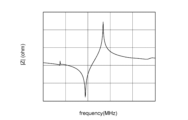
- (Max Phase) 5 and 6 are diagrams showing an example of the characteristics of the resonator 15.
- (ohm) in FIG. 5 indicates the absolute value of the impedance of the resonator 15 .
- the vertical axis Phase (deg) in FIG. 6 indicates the phase of the impedance of the resonator 15 .
- FIGS. 5 and 6 are for explaining general characteristics of elastic wave devices having configurations as shown in FIGS. 3 and 4. FIG. That is, it does not show the characteristics in the examples.
- the phase of the impedance of the resonator 15 approaches 90° in the range between the resonance frequency and the anti-resonance frequency, and -90° in the frequency range outside that range. Get closer. Generally, in the range between the resonance frequency and the anti-resonance frequency, the closer the impedance phase is to 90°, the better the characteristics of the resonator 15 are.
- the phase of the largest impedance is defined as MaxPhase.
- x and y are defined such that the normalized thickness x of the first layer 11 and the normalized thickness y of the second layer 13 are 1 when MaxPhase is maximum. Specifically, it is as follows.
- the inventor performed a simulation calculation to obtain the characteristics of the resonator 15 when the material of the piezoelectric film 7 is LT.
- the simulation was performed under various conditions in which the physical properties and thicknesses of the first layer 11 and the second layer 13 were varied.
- the inventor obtained the MaxPhase of the resonator 15 based on the simulation results for each condition. Using the results, the thickness of the first layer 11 and the thickness of the second layer 13 that maximize the MaxPhase were obtained for each specific value of a plurality of types of physical property values. Below, the said thickness may be called "reference thickness.”
- the inventor was able to clarify the dependence of the reference thickness on the multiple types of physical property values based on the reference thickness for the specific values of the multiple types of physical property values obtained as described above. Furthermore, when specific values were assumed as the physical property values of the first layer 11 and the second layer 13, an approximation formula for calculating the reference thickness corresponding to the specific values could be derived. The thickness calculated using this approximation formula is referred to as "reference thickness".
- the standardized thickness x of the first layer 11 shown in FIG. 1 is obtained by dividing the thickness of the first layer 11 by the reference thickness of the first layer 11 and standardizing it.
- the normalized thickness y of the second layer 13 shown in FIG. 1 is normalized by dividing the thickness of the second layer 13 by the normalized thickness of the second layer 13 .
- MaxPhase is theoretically maximized when each of x and y is 1. However, even if MaxPhase is not the maximum, it is possible to meet the required specifications. Also, when considering the specifications required for characteristics other than MaxPhase, it is not always the case that each of x and y is 1 optimal. Furthermore, since the reference thickness is based on simulation calculations and approximation formulas, there is a possibility that x and y that maximize MaxPhase actually deviate from one. Under these circumstances, the inventor investigated the relationship between changes in the values of x and y and changes in the value of MaxPhase, and defined the range of possible values for x and y. This range is shown in FIG. 1 (and FIG. 11 to be described later).
- ⁇ Second layer 13 Density: various values of 8000 kg/ m3 or more and 10000 kg/ m3 or less Young's modulus: various values of 140 GPa or more and 240 GPa or less Thickness: various values of 0.1 ⁇ m or more and 0.4 ⁇ m or less Number of layers: 4 layers/substrate 3 Material: Si ⁇ IDT electrode 19 Material: Al * There is a Ti layer with a thickness of 6 nm between Al and the piezoelectric film 7 . Thickness: 0.124 ⁇ m Pitch p: 1 ⁇ m Duty: 0.5 *Duty width of electrode finger 27/pitch p Number of electrode fingers 27: infinite (reflector 21 is not assumed.)
- a thickness of 4 ⁇ m of the piezoelectric film 7 corresponds to 0.2 ⁇ . With this thickness, almost no spurious occurs between the resonance frequency and the anti-resonance frequency. This reduces the probability that the value of MaxPhase increases due to spurious. That is, the reliability of analysis using MaxPhase as an evaluation index is high.
- the physical property values (density and Young's modulus) of the first layer 11 and the second layer 13 are set to various values, here, as the material of the first layer 11 and the second layer 13, each physical property A virtual material with values is assumed.
- SiO 2 can be mentioned as a material having a value within the above range of physical property values.
- HfO 2 can be mentioned as a material having values within the range of physical property values described above.
- FIG. 7 is a diagram showing the dependence of the reference thickness (thickness at which MaxPhase is maximized) of the first layer 11 on the physical property values of the multilayer film 5 .
- the horizontal axis Z H indicates the acoustic impedance of the second layer 13 .
- the vertical axis t L ′′ ( ⁇ m) indicates the reference thickness of the first layer 11.
- the plot shows that the Young's modulus E L of the first layer 11 is 55 GPa, They are those at 75 GPa or 95 GPa, and are represented by different shapes depending on the difference in Young's modulus EL .
- the reference thickness t L ′′ of the first layer 11 is correlated to the acoustic impedance Z H of the second layer 13 and to the Young's modulus E L of the first layer 11 .
- the density of the first layer 11 and the thickness of the second layer 13 and the reference thickness t L ′′ was confirmed.
- the correlation between the reference thickness t L ′′ and the acoustic impedance Z H can be represented by an approximate straight line for each value of Young's modulus EL . and the coefficient of determination R2 are shown for each value of Young's modulus E L.
- FIG. 8 is a diagram showing the correlation between the slope m in the above approximation formula and the Young's modulus EL .
- the horizontal axis is Young's modulus E L (GPa).
- the vertical axis is the slope m ( ⁇ m/MRayl). The slopes m of the above three approximation formulas are plotted.
- the correlation between the slope m and Young's modulus EL can be represented by a quadratic approximation curve.
- An approximation formula is shown below.
- FIG. 9 is a diagram showing the correlation between the intercept b in the approximation formula according to FIG. 7 and the Young's modulus EL .
- the horizontal axis is Young's modulus E L (GPa).
- the vertical axis is the intercept b ( ⁇ m).
- the intercepts b of the above three approximation formulas are plotted.
- the correlation between the intercept b and Young's modulus EL can be represented by a quadratic approximation curve.
- An approximation formula is shown below.
- FIG. 10 is a diagram showing the dependence of the reference thickness (thickness at which MaxPhase is maximized) of the second layer 13 on the physical property values of the multilayer film 5 .
- the horizontal axis V H (m/sec) indicates the speed of sound in the second layer 13 .
- the vertical axis t H ′′ ( ⁇ m) indicates the reference thickness of the second layer 13.
- the plot shows that the Young's modulus E L of the first layer 11 is 55 GPa, These are those at 75 GPa or 95 GPa, and are represented by plots of different marks depending on the difference in Young's modulus EL .
- the reference thickness t H ′′ of the second layer 13 correlates to the sound velocity V H of the second layer 13. Also, the reference thickness t H ′′ of the second layer 13 and the No correlation is found between the Young's modulus E L of the first layer 11 . Although not particularly shown, no correlation between the density of the first layer 11 and the thickness of the first layer 11 and the reference thickness t H ′′ was confirmed.
- the correlation between the reference thickness t H ′′ and the sound velocity V H can be represented by an approximate straight line.
- the approximate expression and the coefficient of determination R 2 are shown below.
- the following formula for calculating the reference thickness tL of the first layer 11 is derived from the above approximate formula for calculating the slope m and the intercept b from EL . Further, the following formula for calculating the reference thickness tH of the second layer 13 is derived from the above approximate formula for calculating tH '' from VH .
- the resonance frequency of the Lamb wave here may be affected by various factors such as the influence of the conductive layer 9 and the multilayer film 5.
- the Lamb wave frequency can be obtained by actual measurement or simulation.
- FIG. 1 It is shown by extracting those in which H ' (in other words, x and y) are different from each other.
- H ' in other words, x and y
- the vertical axis, horizontal axis and contour lines in FIG. 1 have already been described.
- the physical property values of the first layer 11 and the second layer 13 in the simulation results extracted in FIG. 1 are as follows. As will be understood from the following, the simulation results are extracted with respect to the central value of the range of physical property values under the current simulation conditions. ⁇ First layer 11 Density: 2400kg/ m3 Young's modulus: 75GPa ⁇ Second layer 13 Density: 9000kg/ m3 Young's modulus: 190GPa
- FIG. 11 is obtained by adding various information (described later) to FIG.
- FIG. 12 corresponds to a cross-sectional view along line XII-XII in FIG.
- FIG. 13 corresponds to a cross-sectional view along line XIII-XIII of FIG.
- the horizontal axis is x or y
- the vertical axis is MaxPhase (deg).
- the values of x and y are in the range in which the value of MaxPhase is 82.2° or more in FIG. ). In this range, PaxPhase is relatively large due to the rapid increase in MaxPhase with changes in x and y, as can be seen from FIGS.
- hatching indicating the range exceeding 82.2° and hatching indicating the range less than 82.2° are attached with the contour line indicating 82.2° between them. Therefore, when the values of x and y are said to be located in the range of 82.2° or more, the values of x and y are located not only on the hatched area indicating the range of more than 82.2°, but also on the range of 82.2°. It may lie on the 2° contour line.
- the range of x and y values using the value of MaxPhase the same applies to other ranges.
- the values of x and y may be located in a range in which the value of MaxPhase is 83.7° or more in FIG. . As can be seen from FIGS. 12 and 13, in this range, the value of MaxPhase is large, and changes in MaxPhase with respect to changes in x and y are gentle.
- the values of x and y may be values that fall within the ellipse ET1 shown in FIG.
- Ellipse ET1 is the smallest ellipse that covers the entire range of 82.2° or more.
- MaxPhase is 79.2° or more within the ellipse ET1.
- the values of x and y may be positioned on the line of the ellipse (the same applies to ellipses other than ellipse ET1).
- the values of x and y may be values that fall within the ellipse ET2 shown in FIG.
- the ellipse ET2 is the largest ellipse within the range of 82.2° or more. Therefore, when the values of x and y fall within the ellipse ET2, the values of x and y are essentially in the range of 82.2° or more.
- the values of x and y may be values that fall within the ellipse ET3 shown in FIG.
- the ellipse ET3 is the smallest ellipse that covers a range of 83.7° or more.
- MaxPhase is 82.2° or more within the ellipse ET3.
- the values of x and y may be values that fall within the ellipse ET4 shown in FIG.
- the ellipse ET4 is the largest ellipse within the range of 83.7° or more. Therefore, when the values of x and y fall within the ellipse ET4, the values of x and y are essentially in the range of 83.7° or more.
- the values of x and y may be values that fall within the circle ET5 shown in FIG.
- FIG. 14 is a diagram showing the dependence of the reference thickness (thickness at which MaxPhase is maximized) of the first layer 11 on the physical property values of the multilayer film 5, and corresponds to FIG.
- FIG. 15 is a diagram showing the correlation between the slope m in the above approximate expression and the Young's modulus EL , and corresponds to FIG.
- FIG. 16 is a diagram showing the correlation between the intercept b in the approximation formula according to FIG. 14 and the Young's modulus EL , and corresponds to FIG.
- FIG. 17 is a diagram showing the dependence of the reference thickness (thickness at which MaxPhase is maximized) of the second layer 13 on the physical property values of the multilayer film 5, and corresponds to FIG.
- t L ⁇ ( ⁇ 2.47 ⁇ 10 ⁇ 7 E L 2 +1.66 ⁇ 10 ⁇ 5 E L ⁇ 2.1 ⁇ 10 ⁇ 3 )Z H + (1.24 ⁇ 10 ⁇ 5 E L 2 +6.85 ⁇ 10 ⁇ 4 E L +1.37 ⁇ 10 ⁇ 1 ) ⁇ ⁇ 5500/fr
- t H (4.34 ⁇ 10 ⁇ 5 V H ⁇ 2.08 ⁇ 10 ⁇ 2 ) ⁇ 5500/fr
- the target resonance frequency fr was 5500 MHz, so 5500/fr is used for generalization.
- Ranges for normalized thicknesses x and y can also be derived in the same manner as for LT. Specifically, it is as follows.
- FIG. 2 shows that the conditions regarding the physical property values of the first layer 11 and the second layer 13 are the same, and the thickness t L ′ of the first layer 11 and the second layer 13, the thickness t H ' (in other words, x and y) is extracted and shown.
- the physical property values of the first layer 11 and the second layer 13 in the extracted simulation results are the same between FIG. 1 and FIG.
- FIG. 18 is obtained by adding various information (described later) to FIG. 2, and corresponds to FIG.
- FIG. 19 corresponds to a cross-sectional view along line XIX-XIX in FIG. 18, and corresponds to FIG.
- FIG. 20 corresponds to a cross-sectional view taken along line XX-XX of FIG. 18, and corresponds to FIG.
- MaxPhase (in other terms x and y) drop sharply when they reach a certain value. Specifically, when the value of MaxPhase falls below 83.4°, the value of MaxPhase drops sharply.
- the values of x and y are in the range in which the value of MaxPhase is 83.4° or more in FIG. ). This range is relatively large in PaxPhase due to the sharp increase in MaxPhase with changes in x and y, similar to the range above 82.2° for LT.
- the values of x and y may be located in a range in which the value of MaxPhase is 84.9° or more in FIG. . In this range, similarly to the range of 83.7° or more in the case of LT, the value of MaxPhase is large and the change of MaxPhase with respect to the change of x and y is moderate.
- the values of x and y may be values that fall within the ellipse EN1 shown in FIG.
- Ellipse EN1 is the smallest ellipse that covers the entire range above 83.4°.
- MaxPhase is 80.4° or more within the ellipse EN1.
- the values of x and y may be values that fall within the ellipse EN2 shown in FIG.
- the ellipse EN2 is the largest ellipse within the range of 83.4° or more. Therefore, when the values of x and y fall within the ellipse EN2, the values of x and y are essentially in the range of 83.4° or more.
- the values of x and y may be values that fall within the ellipse EN3 shown in FIG.
- Ellipse EN3 is the smallest ellipse that covers a range of 84.9° or more.
- MaxPhase is 83.4° or more within the ellipse EN3.
- the values of x and y may be values that fall within the ellipse EN4 shown in FIG. Ellipse EN4 is the largest ellipse that fits in the range of 84.9° or more. Therefore, when the values of x and y fall within ellipse EN4, the values of x and y are essentially in the range of 84.9° or greater.
- the values of x and y may be values that fall within the circle EN5 shown in FIG.
- the elastic wave device 1 has the multilayer film 5, the piezoelectric film 7, and the IDT electrodes 19.
- FIG. The multilayer film 5 is configured by alternately laminating first layers 11 and second layers 13 having an acoustic impedance higher than that of the first layers 11 .
- the piezoelectric film 7 is located on the multilayer film 5 and propagates the A1 mode Lamb wave.
- the IDT electrode 19 is positioned on the piezoelectric film 7 and excites the Lamb wave.
- the normalized thickness of the first layer 11 be x
- the normalized thickness of the second layer 13 be y.
- the values of x and y may be positioned in the range where MaxPhase is 82.2° or more in FIG.
- the values of x and y may be positioned in the range where MaxPhase is 83.4° or more in FIG.
- the values of x and y may be values within any of ellipses (circles) ET1 to ET5.
- the values of x and y may be values within any of ellipses (circles) EN1 to EN5.
- MaxPhase can be increased.
- the loss in the passband of the filter including the resonators 15 (16) can be reduced.
- the material of the multilayer film 5 is not particularly limited.
- the reference thicknesses t L and t H for normalizing x and y are derived from simulation results assuming various materials (virtual materials) having different physical property values (density and Young's modulus) affecting elastic waves. Because From another point of view, when a specific material is selected as the material of the multilayer film 5, x and y are set according to the physical properties of the material.
- the cut angle and thickness of the piezoelectric film 7 and the material and thickness of the IDT electrode 19 are not particularly limited as long as the A1 mode Lamb wave is used. As long as the type of elastic wave is the same (A1 mode Lamb wave), the effect of the interface between the first layer 11 and the second layer 13 on the elastic wave leaked inside the multilayer film 5 is This is because it is thought that it hardly depends on the structure above.
- the difference in the x and y ranges between LT and LN is due to the difference in acoustic impedance at the interface between the piezoelectric film 7 and the multilayer film 5 . Therefore, the difference in the x and y ranges between the LT and LN cases is consistent with the above explanation that the cut angle and thickness of the piezoelectric film 7 and the material and thickness of the IDT electrode 19 are arbitrary. .
- FIG. 21 is a circuit diagram schematically showing the configuration of a demultiplexer 101 as an application example of the elastic wave device 1 (and a filter including the elastic wave device 1).
- the comb-teeth electrode 23 is schematically shown in a bifurcated fork shape, and the reflector 21 is a line with both ends bent. is represented by
- the branching filter 101 includes, for example, a transmission filter 109 that filters a transmission signal from the transmission terminal 105 and outputs it to the antenna terminal 103, and a reception signal that is filtered from the antenna terminal 103 and outputs it to a pair of reception terminals 107. and a reception filter 111 .
- the transmission filter 109 is configured by, for example, a ladder filter configured by connecting a plurality of resonators 15 in a ladder configuration. That is, the transmission filter 109 includes a plurality of (or even one) resonators 15 (series resonators) connected in series between the transmission terminal 105 and the antenna terminal 103, and the series line (series arm). It has a plurality (or even one) of resonators 15 (parallel arms, parallel resonators) connected to the reference potential. Note that the plurality of resonators 15 constituting the transmission filter 109 are provided, for example, on the same fixed substrate 2 (3, 5 and 7).
- the reception filter 111 includes, for example, a resonator 15 and a multimode filter (including a double mode filter) 113 .
- the multimode filter 113 includes a plurality of (three in the illustrated example) IDT electrodes 19 (resonators 16 from another point of view; reference numerals are omitted here) arranged in the propagation direction of elastic waves, and arranged on both sides thereof. and a pair of reflectors 21 . Note that the resonator 15 and the multimode filter 113 that constitute the reception filter 111 are provided on the same fixed substrate 2, for example.
- the transmission filter 109 and the reception filter 111 may be provided on the same fixed substrate 2 or may be provided on different fixed substrates 2 .
- FIG. 21 is merely an example of the configuration of the branching filter 101.
- the reception filter 111 may be configured by a ladder-type filter like the transmission filter 109.
- the series resonators and parallel resonators that constitute one ladder-type filter may be provided on separate fixed substrates 2 .
- the branching filter 101 (multiplexer) is not limited to a duplexer including the transmission filter 109 and the reception filter 111 .
- the demultiplexer may be a diplexer, or may include three or more filters (eg, triplexer or quadplexer). Different from the above description, various filters or the demultiplexer 101 may be regarded as the elastic wave device 1 .
- FIG. 22 is a block diagram showing a main part of a communication device 151 as an example of use of the elastic wave device 1 (branching filter 101).
- the communication device 151 performs wireless communication using radio waves, and includes the branching filter 101 .
- a transmission information signal TIS including information to be transmitted is modulated and frequency-increased (conversion of the carrier frequency to a high-frequency signal) by an RF-IC (Radio Frequency Integrated Circuit) 153 to form a transmission signal TS.
- the transmission signal TS is filtered by the band-pass filter 155 to remove unnecessary components outside the transmission passband, amplified by the amplifier 157, and input to the demultiplexer 101 (transmission terminal 105).
- the demultiplexer 101 (transmission filter 109) removes unnecessary components outside the transmission passband from the input transmission signal TS, and outputs the removed transmission signal TS from the antenna terminal 103 to the antenna 159.
- Antenna 159 converts an input electrical signal (transmission signal TS) into a radio signal (radio waves) and transmits the radio signal.
- a radio signal (radio wave) received by the antenna 159 is converted by the antenna 159 into an electric signal (received signal RS) and input to the branching filter 101 (antenna terminal 103).
- the demultiplexer 101 (receiving filter 111 ) removes unnecessary components outside the pass band for reception from the input received signal RS, and outputs the signal from the receiving terminal 107 to the amplifier 161 .
- the output reception signal RS is amplified by an amplifier 161 and a bandpass filter 163 removes unnecessary components outside the passband for reception. Then, the reception signal RS is subjected to frequency reduction and demodulation by the RF-IC 153 to be a reception information signal RIS.
- the transmission information signal TIS and the reception information signal RIS may be low-frequency signals (baseband signals) containing appropriate information, such as analog audio signals or digitized audio signals.
- the passband of the radio signal may be set as appropriate, and in this embodiment, a relatively high frequency passband (eg, 5 GHz or higher) is also possible.
- the modulation method may be phase modulation, amplitude modulation, frequency modulation, or a combination of two or more of these.
- the direct conversion system is exemplified as the circuit system, but other appropriate systems may be used, such as a double superheterodyne system.
- FIG. 22 schematically shows only the main part, and low-pass filters, isolators, etc. may be added at appropriate positions, and the positions of amplifiers, etc. may be changed.
Landscapes
- Physics & Mathematics (AREA)
- Acoustics & Sound (AREA)
- Surface Acoustic Wave Elements And Circuit Networks Thereof (AREA)
Abstract
Ce dispositif à ondes élastiques comporte un film multicouche, un film piézoélectrique et une électrode IDT. Le film multicouche est configuré par stratification en alternance d'une première couche et d'une seconde couche qui a une impédance acoustique supérieure à celle de la première couche. Le film piézoélectrique est situé au-dessus du film multicouche et permet aux ondes de Lamb d'un mode A1 de se propager. L'électrode IDT est située sur le film piézoélectrique et excite les ondes de Lamb. Lorsque x est une épaisseur normalisée de la première couche et y est une épaisseur normalisée de la seconde couche, les valeurs de x et y peuvent être situées dans la plage où la phase maximale est supérieure ou égale à 82,2° sur la Figure 1 si le matériau du film piézoélectrique est un monocristal de LT. Si le matériau du film piézoélectrique est un monocristal de LN, les valeurs de x et de y peuvent être situées dans la plage où la phase maximale est supérieure ou égale à 83,4° sur la Figure 2.
Applications Claiming Priority (2)
| Application Number | Priority Date | Filing Date | Title |
|---|---|---|---|
| JP2021182309 | 2021-11-09 | ||
| JP2021-182309 | 2021-11-09 |
Publications (1)
| Publication Number | Publication Date |
|---|---|
| WO2023085210A1 true WO2023085210A1 (fr) | 2023-05-19 |
Family
ID=86336018
Family Applications (1)
| Application Number | Title | Priority Date | Filing Date |
|---|---|---|---|
| PCT/JP2022/041167 WO2023085210A1 (fr) | 2021-11-09 | 2022-11-04 | Dispositif à ondes élastiques, filtre, diviseur, et dispositif de communication |
Country Status (1)
| Country | Link |
|---|---|
| WO (1) | WO2023085210A1 (fr) |
Citations (8)
| Publication number | Priority date | Publication date | Assignee | Title |
|---|---|---|---|---|
| JP2006005313A (ja) * | 2004-06-21 | 2006-01-05 | Toshiba Corp | 半導体装置及びその製造方法 |
| WO2012090873A1 (fr) * | 2010-12-28 | 2012-07-05 | 京セラ株式会社 | Élément à ondes élastiques et dispositif à ondes élastiques utilisant celui-ci |
| JP2017149594A (ja) * | 2016-02-22 | 2017-08-31 | 東ソー株式会社 | 酸化物焼結体及び酸化物透明導電膜 |
| JP2017200106A (ja) * | 2016-04-28 | 2017-11-02 | セイコーエプソン株式会社 | 超音波デバイス、超音波モジュール、及び超音波測定装置 |
| JP2017228945A (ja) * | 2016-06-22 | 2017-12-28 | 太陽誘電株式会社 | 弾性波共振器、フィルタおよびマルチプレクサ |
| WO2020100744A1 (fr) * | 2018-11-16 | 2020-05-22 | 株式会社村田製作所 | Dispositif à ondes élastiques |
| WO2021079830A1 (fr) * | 2019-10-24 | 2021-04-29 | 京セラ株式会社 | Dispositif à ondes élastiques |
| JP2021150893A (ja) * | 2020-03-23 | 2021-09-27 | 京セラ株式会社 | フィルタ、分波器及び通信装置 |
-
2022
- 2022-11-04 WO PCT/JP2022/041167 patent/WO2023085210A1/fr unknown
Patent Citations (8)
| Publication number | Priority date | Publication date | Assignee | Title |
|---|---|---|---|---|
| JP2006005313A (ja) * | 2004-06-21 | 2006-01-05 | Toshiba Corp | 半導体装置及びその製造方法 |
| WO2012090873A1 (fr) * | 2010-12-28 | 2012-07-05 | 京セラ株式会社 | Élément à ondes élastiques et dispositif à ondes élastiques utilisant celui-ci |
| JP2017149594A (ja) * | 2016-02-22 | 2017-08-31 | 東ソー株式会社 | 酸化物焼結体及び酸化物透明導電膜 |
| JP2017200106A (ja) * | 2016-04-28 | 2017-11-02 | セイコーエプソン株式会社 | 超音波デバイス、超音波モジュール、及び超音波測定装置 |
| JP2017228945A (ja) * | 2016-06-22 | 2017-12-28 | 太陽誘電株式会社 | 弾性波共振器、フィルタおよびマルチプレクサ |
| WO2020100744A1 (fr) * | 2018-11-16 | 2020-05-22 | 株式会社村田製作所 | Dispositif à ondes élastiques |
| WO2021079830A1 (fr) * | 2019-10-24 | 2021-04-29 | 京セラ株式会社 | Dispositif à ondes élastiques |
| JP2021150893A (ja) * | 2020-03-23 | 2021-09-27 | 京セラ株式会社 | フィルタ、分波器及び通信装置 |
Similar Documents
| Publication | Publication Date | Title |
|---|---|---|
| JP7433268B2 (ja) | 弾性波装置、分波器および通信装置 | |
| JP6856825B2 (ja) | 弾性波装置、分波器および通信装置 | |
| US10879870B2 (en) | Elastic wave device, front-end circuit, and communication device | |
| JP6247377B2 (ja) | 弾性波素子、フィルタ素子および通信装置 | |
| JP6573668B2 (ja) | 弾性波装置および通信装置 | |
| WO2016104598A1 (fr) | Dispositif à onde acoustique | |
| KR102140089B1 (ko) | 탄성파 공진기, 필터 및 멀티플렉서 | |
| JP7278305B2 (ja) | 弾性波装置、分波器および通信装置 | |
| US20240030891A1 (en) | Elastic wave element and communication device | |
| JPWO2019022236A1 (ja) | 弾性波装置、分波器および通信装置 | |
| CN110710106B (zh) | 弹性波装置、分波器及通信装置 | |
| US11863155B2 (en) | Surface acoustic wave element | |
| JP7117880B2 (ja) | 弾性波フィルタ、分波器および通信装置 | |
| WO2023085210A1 (fr) | Dispositif à ondes élastiques, filtre, diviseur, et dispositif de communication | |
| US20220345112A1 (en) | Acoustic wave filter and communication apparatus | |
| JP7421557B2 (ja) | 弾性波装置及び通信装置 | |
| WO2023167221A1 (fr) | Substrat composite, élément à ondes acoustiques, module et dispositif de communication | |
| WO2023176814A1 (fr) | Filtre en échelle, module et dispositif de communication | |
| WO2023033032A1 (fr) | Élément à ondes élastiques, démultiplexeur et dispositif de communication | |
| WO2023210524A1 (fr) | Élément à ondes élastiques et dispositif de communication | |
| WO2023286704A1 (fr) | Dispositif à ondes élastiques, diviseur, et dispositif de communication | |
| JP7037439B2 (ja) | 弾性波素子、分波器および通信装置 | |
| CN115769492A (zh) | 弹性波装置以及通信装置 |
Legal Events
| Date | Code | Title | Description |
|---|---|---|---|
| 121 | Ep: the epo has been informed by wipo that ep was designated in this application |
Ref document number: 22892709 Country of ref document: EP Kind code of ref document: A1 |
|
| ENP | Entry into the national phase |
Ref document number: 2023559606 Country of ref document: JP Kind code of ref document: A |