WO2020100744A1 - Dispositif à ondes élastiques - Google Patents
Dispositif à ondes élastiques Download PDFInfo
- Publication number
- WO2020100744A1 WO2020100744A1 PCT/JP2019/043906 JP2019043906W WO2020100744A1 WO 2020100744 A1 WO2020100744 A1 WO 2020100744A1 JP 2019043906 W JP2019043906 W JP 2019043906W WO 2020100744 A1 WO2020100744 A1 WO 2020100744A1
- Authority
- WO
- WIPO (PCT)
- Prior art keywords
- dielectric film
- wave device
- electrode fingers
- gap
- electrode
- Prior art date
Links
- 239000000758 substrate Substances 0.000 claims abstract description 68
- VYPSYNLAJGMNEJ-UHFFFAOYSA-N Silicium dioxide Chemical compound O=[Si]=O VYPSYNLAJGMNEJ-UHFFFAOYSA-N 0.000 claims abstract description 17
- 229910052814 silicon oxide Inorganic materials 0.000 claims abstract description 14
- 230000001902 propagating effect Effects 0.000 claims description 10
- 239000010410 layer Substances 0.000 description 56
- 239000000463 material Substances 0.000 description 31
- 230000000052 comparative effect Effects 0.000 description 25
- 229910052751 metal Inorganic materials 0.000 description 18
- 239000002184 metal Substances 0.000 description 18
- XUIMIQQOPSSXEZ-UHFFFAOYSA-N Silicon Chemical compound [Si] XUIMIQQOPSSXEZ-UHFFFAOYSA-N 0.000 description 11
- 239000010703 silicon Substances 0.000 description 11
- 229910052710 silicon Inorganic materials 0.000 description 11
- 229910052581 Si3N4 Inorganic materials 0.000 description 9
- HQVNEWCFYHHQES-UHFFFAOYSA-N silicon nitride Chemical group N12[Si]34N5[Si]62N3[Si]51N64 HQVNEWCFYHHQES-UHFFFAOYSA-N 0.000 description 9
- CPLXHLVBOLITMK-UHFFFAOYSA-N Magnesium oxide Chemical compound [Mg]=O CPLXHLVBOLITMK-UHFFFAOYSA-N 0.000 description 8
- 238000010586 diagram Methods 0.000 description 8
- 230000004048 modification Effects 0.000 description 8
- 238000012986 modification Methods 0.000 description 8
- 229910004298 SiO 2 Inorganic materials 0.000 description 6
- MCMNRKCIXSYSNV-UHFFFAOYSA-N Zirconium dioxide Chemical compound O=[Zr]=O MCMNRKCIXSYSNV-UHFFFAOYSA-N 0.000 description 6
- 239000013078 crystal Substances 0.000 description 5
- WSMQKESQZFQMFW-UHFFFAOYSA-N 5-methyl-pyrazole-3-carboxylic acid Chemical compound CC1=CC(C(O)=O)=NN1 WSMQKESQZFQMFW-UHFFFAOYSA-N 0.000 description 4
- GQYHUHYESMUTHG-UHFFFAOYSA-N lithium niobate Chemical compound [Li+].[O-][Nb](=O)=O GQYHUHYESMUTHG-UHFFFAOYSA-N 0.000 description 4
- 239000000395 magnesium oxide Substances 0.000 description 4
- BPUBBGLMJRNUCC-UHFFFAOYSA-N oxygen(2-);tantalum(5+) Chemical compound [O-2].[O-2].[O-2].[O-2].[O-2].[Ta+5].[Ta+5] BPUBBGLMJRNUCC-UHFFFAOYSA-N 0.000 description 4
- HBMJWWWQQXIZIP-UHFFFAOYSA-N silicon carbide Chemical compound [Si+]#[C-] HBMJWWWQQXIZIP-UHFFFAOYSA-N 0.000 description 4
- 229910010271 silicon carbide Inorganic materials 0.000 description 4
- PNEYBMLMFCGWSK-UHFFFAOYSA-N aluminium oxide Inorganic materials [O-2].[O-2].[O-2].[Al+3].[Al+3] PNEYBMLMFCGWSK-UHFFFAOYSA-N 0.000 description 3
- PMHQVHHXPFUNSP-UHFFFAOYSA-M copper(1+);methylsulfanylmethane;bromide Chemical compound Br[Cu].CSC PMHQVHHXPFUNSP-UHFFFAOYSA-M 0.000 description 3
- 229910052878 cordierite Inorganic materials 0.000 description 3
- 239000010432 diamond Substances 0.000 description 3
- 229910003460 diamond Inorganic materials 0.000 description 3
- JSKIRARMQDRGJZ-UHFFFAOYSA-N dimagnesium dioxido-bis[(1-oxido-3-oxo-2,4,6,8,9-pentaoxa-1,3-disila-5,7-dialuminabicyclo[3.3.1]nonan-7-yl)oxy]silane Chemical compound [Mg++].[Mg++].[O-][Si]([O-])(O[Al]1O[Al]2O[Si](=O)O[Si]([O-])(O1)O2)O[Al]1O[Al]2O[Si](=O)O[Si]([O-])(O1)O2 JSKIRARMQDRGJZ-UHFFFAOYSA-N 0.000 description 3
- KZHJGOXRZJKJNY-UHFFFAOYSA-N dioxosilane;oxo(oxoalumanyloxy)alumane Chemical compound O=[Si]=O.O=[Si]=O.O=[Al]O[Al]=O.O=[Al]O[Al]=O.O=[Al]O[Al]=O KZHJGOXRZJKJNY-UHFFFAOYSA-N 0.000 description 3
- 229910052839 forsterite Inorganic materials 0.000 description 3
- HCWCAKKEBCNQJP-UHFFFAOYSA-N magnesium orthosilicate Chemical compound [Mg+2].[Mg+2].[O-][Si]([O-])([O-])[O-] HCWCAKKEBCNQJP-UHFFFAOYSA-N 0.000 description 3
- 229910052863 mullite Inorganic materials 0.000 description 3
- TWNQGVIAIRXVLR-UHFFFAOYSA-N oxo(oxoalumanyloxy)alumane Chemical compound O=[Al]O[Al]=O TWNQGVIAIRXVLR-UHFFFAOYSA-N 0.000 description 3
- 239000010453 quartz Substances 0.000 description 3
- 239000010980 sapphire Substances 0.000 description 3
- 229910052594 sapphire Inorganic materials 0.000 description 3
- -1 steatite Chemical compound 0.000 description 3
- PBCFLUZVCVVTBY-UHFFFAOYSA-N tantalum pentoxide Inorganic materials O=[Ta](=O)O[Ta](=O)=O PBCFLUZVCVVTBY-UHFFFAOYSA-N 0.000 description 3
- OKTJSMMVPCPJKN-UHFFFAOYSA-N Carbon Chemical compound [C] OKTJSMMVPCPJKN-UHFFFAOYSA-N 0.000 description 2
- 229910052799 carbon Inorganic materials 0.000 description 2
- 239000000919 ceramic Substances 0.000 description 2
- 239000010408 film Substances 0.000 description 2
- 239000011521 glass Substances 0.000 description 2
- 238000004519 manufacturing process Methods 0.000 description 2
- 239000000203 mixture Substances 0.000 description 2
- ZOXJGFHDIHLPTG-UHFFFAOYSA-N Boron Chemical compound [B] ZOXJGFHDIHLPTG-UHFFFAOYSA-N 0.000 description 1
- PXGOKWXKJXAPGV-UHFFFAOYSA-N Fluorine Chemical compound FF PXGOKWXKJXAPGV-UHFFFAOYSA-N 0.000 description 1
- CFJRGWXELQQLSA-UHFFFAOYSA-N azanylidyneniobium Chemical compound [Nb]#N CFJRGWXELQQLSA-UHFFFAOYSA-N 0.000 description 1
- 229910052796 boron Inorganic materials 0.000 description 1
- 150000001875 compounds Chemical class 0.000 description 1
- 239000003989 dielectric material Substances 0.000 description 1
- 229910052731 fluorine Inorganic materials 0.000 description 1
- 239000011737 fluorine Substances 0.000 description 1
- 229910000449 hafnium oxide Inorganic materials 0.000 description 1
- WIHZLLGSGQNAGK-UHFFFAOYSA-N hafnium(4+);oxygen(2-) Chemical compound [O-2].[O-2].[Hf+4] WIHZLLGSGQNAGK-UHFFFAOYSA-N 0.000 description 1
- 230000001681 protective effect Effects 0.000 description 1
- LIVNPJMFVYWSIS-UHFFFAOYSA-N silicon monoxide Chemical compound [Si-]#[O+] LIVNPJMFVYWSIS-UHFFFAOYSA-N 0.000 description 1
- 239000002356 single layer Substances 0.000 description 1
- 229910052596 spinel Inorganic materials 0.000 description 1
- 239000011029 spinel Substances 0.000 description 1
- 229910001936 tantalum oxide Inorganic materials 0.000 description 1
- ZCUFMDLYAMJYST-UHFFFAOYSA-N thorium dioxide Chemical compound O=[Th]=O ZCUFMDLYAMJYST-UHFFFAOYSA-N 0.000 description 1
- 229910003452 thorium oxide Inorganic materials 0.000 description 1
Images


Classifications
-
- H—ELECTRICITY
- H03—ELECTRONIC CIRCUITRY
- H03H—IMPEDANCE NETWORKS, e.g. RESONANT CIRCUITS; RESONATORS
- H03H9/00—Networks comprising electromechanical or electro-acoustic devices; Electromechanical resonators
- H03H9/02—Details
- H03H9/02535—Details of surface acoustic wave devices
- H03H9/02543—Characteristics of substrate, e.g. cutting angles
- H03H9/02574—Characteristics of substrate, e.g. cutting angles of combined substrates, multilayered substrates, piezoelectrical layers on not-piezoelectrical substrate
-
- H—ELECTRICITY
- H03—ELECTRONIC CIRCUITRY
- H03H—IMPEDANCE NETWORKS, e.g. RESONANT CIRCUITS; RESONATORS
- H03H9/00—Networks comprising electromechanical or electro-acoustic devices; Electromechanical resonators
- H03H9/02—Details
- H03H9/02535—Details of surface acoustic wave devices
- H03H9/02637—Details concerning reflective or coupling arrays
-
- H—ELECTRICITY
- H03—ELECTRONIC CIRCUITRY
- H03H—IMPEDANCE NETWORKS, e.g. RESONANT CIRCUITS; RESONATORS
- H03H9/00—Networks comprising electromechanical or electro-acoustic devices; Electromechanical resonators
- H03H9/02—Details
- H03H9/02535—Details of surface acoustic wave devices
- H03H9/02818—Means for compensation or elimination of undesirable effects
- H03H9/02866—Means for compensation or elimination of undesirable effects of bulk wave excitation and reflections
-
- H—ELECTRICITY
- H03—ELECTRONIC CIRCUITRY
- H03H—IMPEDANCE NETWORKS, e.g. RESONANT CIRCUITS; RESONATORS
- H03H9/00—Networks comprising electromechanical or electro-acoustic devices; Electromechanical resonators
- H03H9/02—Details
- H03H9/02535—Details of surface acoustic wave devices
- H03H9/02992—Details of bus bars, contact pads or other electrical connections for finger electrodes
-
- H—ELECTRICITY
- H03—ELECTRONIC CIRCUITRY
- H03H—IMPEDANCE NETWORKS, e.g. RESONANT CIRCUITS; RESONATORS
- H03H9/00—Networks comprising electromechanical or electro-acoustic devices; Electromechanical resonators
- H03H9/02—Details
- H03H9/125—Driving means, e.g. electrodes, coils
- H03H9/145—Driving means, e.g. electrodes, coils for networks using surface acoustic waves
- H03H9/14538—Formation
- H03H9/14541—Multilayer finger or busbar electrode
-
- H—ELECTRICITY
- H03—ELECTRONIC CIRCUITRY
- H03H—IMPEDANCE NETWORKS, e.g. RESONANT CIRCUITS; RESONATORS
- H03H9/00—Networks comprising electromechanical or electro-acoustic devices; Electromechanical resonators
- H03H9/02—Details
- H03H9/125—Driving means, e.g. electrodes, coils
- H03H9/145—Driving means, e.g. electrodes, coils for networks using surface acoustic waves
- H03H9/14544—Transducers of particular shape or position
- H03H9/14558—Slanted, tapered or fan shaped transducers
-
- H—ELECTRICITY
- H03—ELECTRONIC CIRCUITRY
- H03H—IMPEDANCE NETWORKS, e.g. RESONANT CIRCUITS; RESONATORS
- H03H9/00—Networks comprising electromechanical or electro-acoustic devices; Electromechanical resonators
- H03H9/25—Constructional features of resonators using surface acoustic waves
Definitions
- the present invention relates to an acoustic wave device.
- Patent Document 1 discloses an example of an acoustic wave device.
- This acoustic wave device has a laminated body in which a low acoustic velocity film and a piezoelectric film are laminated in this order on a high acoustic velocity support substrate, and an IDT electrode provided on the piezoelectric film.
- the acoustic wave device having the above-mentioned laminated body can increase the Q value, but has a problem that transverse mode ripples occur.
- the IDT electrode is a tilted IDT electrode in order to suppress the transverse mode ripple.
- the tilted IDT electrode refers to an envelope line that is a virtual line formed by connecting the tips of a plurality of electrode fingers connected to one bus bar and the tips of a plurality of electrode fingers connected to the other bus bar.
- An envelope, which is a virtual line formed by connecting the IDT electrodes, extends obliquely with respect to the elastic wave propagation direction.
- An object of the present invention is to provide an elastic wave device capable of suppressing ripples near the resonance frequency.
- An acoustic wave device includes a piezoelectric substrate and an IDT electrode provided on the piezoelectric substrate, the piezoelectric substrate being a high sonic layer and directly or indirectly on the high sonic layer.
- the piezoelectric substrate being a high sonic layer and directly or indirectly on the high sonic layer.
- the IDT electrodes face each other.
- a second envelope, which is an imaginary line formed by connecting the tips of the plurality of second electrode fingers, is inclined with respect to the elastic wave propagation direction.
- the first dielectric film is provided in at least one of the plurality of second gaps located between the first dielectric film and the first bus bar, and the density of the first dielectric film is higher than that of silicon oxide. ..
- an elastic wave device capable of suppressing ripples near the resonance frequency.
- FIG. 1 is a front sectional view of an acoustic wave device according to a first embodiment of the present invention.
- FIG. 2 is a plan view of the elastic wave device according to the first embodiment of the present invention.
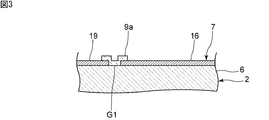
- FIG. 3 is a cross-sectional view showing the vicinity of the first gap of the IDT electrode according to the first embodiment of the present invention and showing a cross section taken along the line II in FIG.
- FIG. 4 is a plan view for explaining a modified example of the IDT electrode of the acoustic wave device of the first embodiment.
- FIG. 5 is a plan view of an elastic wave device according to a first comparative example.
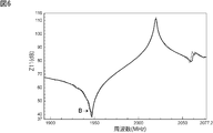
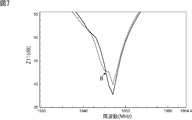
- FIG. 6 is a diagram showing impedance characteristics in the first embodiment of the present invention and the first comparative example.
- FIG. 1 is a front sectional view of an acoustic wave device according to a first embodiment of the present invention.
- FIG. 2 is a plan view of the elastic wave device according to the first embodiment of the present invention.
- FIG. 3 is
- FIG. 7 is a diagram showing impedance characteristics near the resonance frequency in the first embodiment and the first comparative example of the present invention.
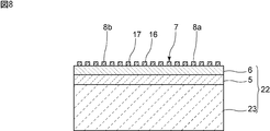
- FIG. 8 is a front sectional view of an elastic wave device according to a first modification of the first embodiment of the present invention.
- FIG. 9 is a front sectional view of an elastic wave device according to a second modification of the first embodiment of the present invention.
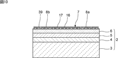
- FIG. 10 is a front sectional view of an acoustic wave device according to a second embodiment of the present invention.
- FIG. 11 is a sectional view showing the vicinity of the first gap of the IDT electrode according to the second embodiment of the present invention.
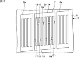
- FIG. 12 is a plan view of an elastic wave device according to a third embodiment of the present invention.
- FIG. 13 is a sectional view showing the vicinity of the first gap of the IDT electrode according to the third embodiment of the present invention.
- FIG. 14 is a diagram showing impedance characteristics in the third embodiment of the present invention and the second comparative example.
- FIG. 15 is a diagram showing impedance characteristics near the resonance frequency in the third embodiment and the second comparative example of the present invention.
- FIG. 1 is a front sectional view of an acoustic wave device according to a first embodiment of the present invention.
- the acoustic wave device 1 has a piezoelectric substrate 2.
- the piezoelectric substrate 2 is provided on the support substrate 3, the high sonic film 4 provided on the support substrate 3, the low sonic film 5 provided on the high sonic film 4, and the low sonic film 5.
- the piezoelectric layer 6 is a lithium tantalate film in this embodiment. More specifically, the piezoelectric layer 6 is made of 50 ° YX-LiTaO 3 .
- the cut angle of the piezoelectric layer 6 is not limited to the above, and the material of the piezoelectric layer 6 is not limited to the above.
- the piezoelectric layer 6 may include, for example, a piezoelectric single crystal such as lithium niobate or an appropriate piezoelectric ceramic as a main component.
- the IDT electrode 7 is provided on the piezoelectric layer 6 of the piezoelectric substrate 2. By applying an AC voltage to the IDT electrode 7, elastic waves are excited. A pair of reflectors 8a and 8b are provided on both sides of the IDT electrode 7 in the elastic wave propagation direction on the piezoelectric layer 6.
- the elastic wave device 1 of the present embodiment is an elastic wave resonator.
- the elastic wave device according to the present invention may be a filter device such as a ladder filter including an elastic wave resonator.
- the low acoustic velocity film 5 is a relatively low acoustic velocity film. More specifically, the sound velocity of the bulk wave propagating through the low acoustic velocity film 5 is lower than the sound velocity of the bulk wave propagating through the piezoelectric layer 6.
- the low acoustic velocity film 5 contains silicon oxide represented by SiO x as a main component. x is an arbitrary positive value. In this embodiment, the low acoustic velocity film 5 is a SiO 2 film.
- the material of the low acoustic velocity film 5 is not limited to the above, and for example, silicon oxide, glass, silicon oxynitride, tantalum oxide, or a material containing a compound of fluorine, carbon, or boron added to silicon oxide as a main component is used. It can also be used.
- the high sound velocity layer in the present invention is the high sound velocity film 4.
- the high sound velocity layer is a layer having a relatively high sound velocity. More specifically, the acoustic velocity of the bulk wave propagating in the high acoustic velocity layer is higher than the acoustic velocity of the elastic wave propagating in the piezoelectric layer 6.
- the high sound velocity film 4 as the high sound velocity layer is a silicon nitride film.
- the material of the high sonic velocity film 4 is not limited to the above, and examples thereof include lithium tantalate, lithium niobate, piezoelectric materials such as quartz, alumina, zirconia, cordierite, mullite, steatite, and forsterite.
- a material containing the main component can also be used.
- the support substrate 3 is a silicon substrate in this embodiment. More specifically, the crystal orientation of the support substrate 3 is Si (100).
- the Euler angles ( ⁇ , ⁇ , ⁇ ) of the support substrate 3 are Euler angles (0 °, 0 °, 45 °).
- the crystal orientation and Euler angles ( ⁇ , ⁇ , ⁇ ) of the support substrate 3 are not limited to the above, and the material of the support substrate 3 is not limited to the above. Examples of the material of the support substrate 3 include lithium tantalate, lithium niobate, piezoelectric materials such as quartz, alumina, magnesia, silicon nitride, aluminum nitride, silicon carbide, zirconia, cordierite, mullite, steatite, and forsterite.
- the acoustic wave device 1 has the piezoelectric substrate 2 including a laminated body in which the high acoustic velocity film 4, the low acoustic velocity film 5 and the piezoelectric layer 6 are laminated in this order. Thereby, the energy of the elastic wave can be effectively trapped on the piezoelectric layer 6 side.
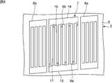
- FIG. 2 is a plan view of the acoustic wave device according to the first embodiment.
- the IDT electrode 7 has a first bus bar 14 and a second bus bar 15 facing each other.
- the IDT electrode 7 has a plurality of first electrode fingers 16 whose one end is connected to the first bus bar 14 and a plurality of second electrode fingers 17 whose one end is connected to the second bus bar 15.
- the plurality of first electrode fingers 16 and the plurality of second electrode fingers 17 are interleaved with each other.
- the IDT electrode 7 has a plurality of first dummy electrode fingers 18 whose one end is connected to the first bus bar 14.
- the plurality of first dummy electrode fingers 18 face the plurality of second electrode fingers 17 via the second gap G2.
- the IDT electrode 7 has a plurality of second dummy electrode fingers 19 whose one end is connected to the second bus bar 15.
- the plurality of second dummy electrode fingers 19 face the plurality of first electrode fingers 16 via the first gap G1.
- the first envelope A1 that is a virtual line formed by connecting the tips of the plurality of first electrode fingers 16 extends obliquely with respect to the elastic wave propagation direction.
- the second envelope A2 which is a virtual line formed by connecting the tips of the plurality of second electrode fingers 17, extends obliquely with respect to the elastic wave propagation direction.
- the IDT electrode 7 is a tilted IDT electrode.
- the inclination angle in which the direction in which the first envelope A1 and the second envelope A2 extend is inclined with respect to the elastic wave propagation direction is not particularly limited, but in the present embodiment, the inclination angle is 7.5 °. ..
- the plurality of first gaps G1 are located between the plurality of first electrode fingers 16 and the plurality of second dummy electrode fingers 19.
- the plurality of second gaps G2 are located between the plurality of second electrode fingers 17 and the plurality of first dummy electrode fingers 18.
- the plurality of first gaps G1 may be located between the plurality of first electrode fingers 16 and the second bus bar 15, and the plurality of second gaps G2 may be arranged between the plurality of second electrode fingers. It may be located between 17 and the first bus bar 14.
- the IDT electrode 7 is composed of a laminated metal film in which a Ti layer, an Al layer and a Ti layer are laminated in this order from the piezoelectric substrate 2 side.
- the reflector 8a and the reflector 8b are also made of the same laminated metal film as the IDT electrode 7.
- the materials of the IDT electrode 7, the reflector 8a, and the reflector 8b and the number of metal layers are not limited to the above.
- the IDT electrode 7, the reflector 8a and the reflector 8b may be made of a single layer metal film.
- FIG. 3 is a cross-sectional view showing the vicinity of the first gap of the IDT electrode in the first embodiment, showing a cross section taken along the line II in FIG.
- First dielectric films 9a are provided in the plurality of first gaps G1 on the piezoelectric substrate 2. More specifically, the plurality of first dielectric films 9a are provided so as to reach the entire plurality of first gaps G1. The plurality of first dielectric films 9 a reach the first electrode fingers 16 and the second dummy electrode fingers 19. The first dielectric film 9a is continuously provided near the tip on the first electrode finger 16 and near the tip on the first gap G1 and the second dummy electrode finger 19. The first dielectric film 9a may be provided on at least a part of the first gap G1.
- the plurality of first dielectric films 9b are provided so as to reach the entire plurality of second gaps G2.
- the plurality of first dielectric films 9b reach the second electrode fingers 17 and the first dummy electrode fingers 18. More specifically, the first dielectric film 9b is continuously provided near the tip on the second electrode finger 17, near the tip on the second gap G2, and the first dummy electrode finger 18. There is.
- the first dielectric film 9b may be provided on at least a part of the second gap G2.
- the first dummy electrode finger 18 and the second dummy electrode finger 19 may not be provided. That is, unlike the modification of the IDT electrode 7 shown in FIG. 4, the first dummy electrode finger 18 and the second dummy electrode finger 19 may not be provided.
- the plurality of first dielectric films 9 a are provided on the second bus bar 15 from above the first electrode finger 16 through the gap between the first electrode finger 16 and the second bus bar 15. It is provided to reach.
- the second dielectric film 9b extends from above the second electrode finger 17 to above the first bus bar 14 through the gap between the second electrode finger 17 and the first bus bar 14. It is provided in.
- the first dielectric film 9a is provided in all the first gaps G1 and the first dielectric film 9b is provided in all the second gaps G2.
- the first dielectric film 9a and the first dielectric film 9b do not necessarily have to be provided in all the first gaps G1 and the second gaps G2.
- the first dielectric film 9a or the first dielectric film 9b may be provided in at least one of the plurality of first gaps G1 and the plurality of second gaps G2.
- the first dielectric film 9a and the first dielectric film 9b are tantalum pentoxide films in this embodiment.
- the density of the first dielectric film 9a and the first dielectric film 9b is not limited to this, and may be higher than the density of silicon oxide.
- the silicon oxide that is the object of density comparison in this specification is SiO 2 .
- the density of silicon oxide in this specification is 2.21 ⁇ 10 3 [kg / m 3 ].
- the dielectric material forming the first dielectric film 9a and the first dielectric film 9b for example, hafnium oxide, thorium oxide, or niobium nitride can be used.
- the feature of this embodiment is that it has the following configuration. 1) A piezoelectric substrate 2 including a laminated body in which a high sonic velocity film 4, a low sonic velocity film 5 and a piezoelectric layer 6 are laminated in this order, and an inclined IDT electrode 7 provided on the piezoelectric substrate 2. Have. 2) A plurality of first dielectric films 9a and a plurality of first dielectric films 9b having a density higher than that of silicon oxide are provided in the plurality of first gaps G1 and the plurality of second gaps G2 of the IDT electrode 7. It is provided. Thereby, the ripple near the resonance frequency can be suppressed. This will be described below by comparing the present embodiment with a comparative example.
- the acoustic wave device 101 of the first comparative example is different from the acoustic wave device 101 of the first embodiment except that it does not have the first dielectric film 9a and the first dielectric film 9b. It has the same configuration as the acoustic wave device 1 of the first embodiment.
- the elastic wave device having the configuration of the first embodiment and the elastic wave device of the first comparative example were manufactured.
- the conditions of the elastic wave device having the configuration of the first embodiment and the elastic wave device of the first comparative example are as follows.
- the wavelength described below is a wavelength defined by the electrode finger pitch of the IDT electrodes.
- a region where adjacent electrode fingers overlap is defined as an intersecting region of the IDT electrodes
- a length of the intersecting region along the extending direction of the electrode fingers is defined as a intersecting width.
- the length of the first gap along the direction in which the electrode fingers extend is the first gap width
- the length of the second gap along the direction in which the electrode fingers extend is the second gap width.
- Piezoelectric layer material 50 ° YX-LiTaO 3 , film thickness 600 nm Low sonic film: Silicon oxide (SiO 2 ) material, film thickness 673 nm High sonic film: Material silicon nitride (SiN), film thickness 900nm Support substrate: Material silicon (Si), crystal orientation Si (100), Euler angle (0 °, 0 °, 45 °) Thickness of each metal layer of the IDT electrode: thickness of the Ti layer on the piezoelectric layer side is 12 nm, thickness of the Al layer is 100 nm, thickness of the Ti layer is 4 nm. Wavelength: 2 ⁇ m Cross width: 30 ⁇ m Number of pairs of electrode fingers of the IDT electrode: 100 pairs Inclination angle: 7.5 ° First gap width and second gap width: 0.27 ⁇ m
- the conditions of the first dielectric film of the acoustic wave device having the configuration of the first embodiment are as follows.
- First dielectric film material; tantalum pentoxide (Ta 2 O 5 ), density 8.47 ⁇ 10 3 [kg / m 3 ], film thickness 30 nm
- each acoustic wave device The impedance characteristics of each acoustic wave device are shown in FIGS. 6 and 7 below.
- FIG. 6 is a diagram showing impedance characteristics in the first embodiment and the first comparative example.
- FIG. 7 is a diagram showing impedance characteristics near the resonance frequency in the first embodiment and the first comparative example. 6 and 7, the solid line shows the result of the first embodiment, and the broken line shows the result of the first comparative example.
- ripples between the resonance frequency and the anti-resonance frequency are suppressed as shown in FIG.
- ripples occur near the resonance frequency in the first comparative example.
- ripples near the resonance frequency do not occur.
- the ripple near the resonance frequency in addition to suppressing the ripple between the resonance frequency and the anti-resonance frequency, the ripple near the resonance frequency can be suppressed.
- the first comparative example by having the same piezoelectric substrate 2 as in the first embodiment, not only the acoustic wave used as the main mode by the acoustic wave device but also the unnecessary wave that causes ripples is located on the piezoelectric layer side. It becomes easy to be trapped in. Further, the first electrode finger 16 and the second dummy electrode finger 19 are discontinuous with the first gap G1 therebetween. Therefore, the sound velocity in the region where the IDT electrode 7 is provided has discontinuity in the vicinity of the first gap G1. Similarly, the sound velocity in the area where the IDT electrode 7 is provided has discontinuity even in the vicinity of the second gap G2. It is considered that the ripple of the first comparative example is caused by the mode confined in the vicinity of the first gap G1 and the second gap G2 of the tilted IDT electrode 7.
- the first dielectric film 9a is provided in the first gap G1.
- the density of the first dielectric film 9a is higher than that of silicon oxide.
- the density of the first dielectric film 9a can be effectively made close to the density of the IDT electrode 7, or can be made higher than the density of the IDT electrode 7.
- the state of mass addition in the first gap G1 can be effectively brought close to the state of mass addition in the portion where the first electrode finger 16 and the second dummy electrode finger 19 are provided.
- the sound velocity in the area in which the first gap G1 is arranged is effectively brought close to the sound velocity in the area in which the first electrode finger 16 is provided and the area in which the second dummy electrode finger 19 is provided. be able to. Therefore, the discontinuity between the first electrode finger 16 and the second dummy electrode finger 19 in the first gap G1 can be reduced.
- the discontinuity between the second electrode finger 17 and the first dummy electrode finger 18 in the second gap G2. can be made smaller. Therefore, mode confinement in the first gap G1 and the second gap G2 can be suppressed. Therefore, the ripple near the resonance frequency can be suppressed.
- the densities of the first dielectric film 9a and the first dielectric film 9b are preferably equal to or higher than the density of the material of the IDT electrode 7.
- the state of mass addition in the first gap G1 can be more surely brought closer to the state of mass addition in the portion where the first electrode finger 16 and the second dummy electrode finger 19 are provided. it can.
- the density of the first dielectric film 9a and the first dielectric film 9b is higher than that of the IDT electrode 7, the thickness of the first dielectric film 9a is smaller than that of the IDT electrode 7.
- the mass addition state in the first gap G1 can be effectively brought close to the mass addition state in the portion where the first electrode finger 16 and the second dummy electrode finger 19 are provided.
- the state of mass addition in the second gap G2 can be more reliably approximated to the state of mass addition in the portion where the second electrode finger 17 and the first dummy electrode finger 18 are provided. Therefore, mode confinement in the first gap G1 and the second gap G2 can be more reliably suppressed, and ripples near the resonance frequency can be more reliably suppressed.
- the average density of the laminated metal film and the densities of the first dielectric film 9a and the first dielectric film 9b may be compared.
- the average density of the laminated metal film may be calculated as follows. In each metal layer of the laminated metal film, the film thickness ratio of the metal layer, which is a value obtained by dividing the film thickness of the metal layer by the film thickness of the entire laminated metal film, is calculated. Next, the product of the film thickness ratio and the density is calculated for each metal layer. Then, the products in all metal layers are added together.
- the densities of the first dielectric film 9a and the first dielectric film 9b are preferably equal to or higher than the densities of the first electrode finger 16 and the second electrode finger 17. Accordingly, even when the metal layers forming the first electrode fingers 16 and the second electrode fingers 17 are different from the metal layers forming the first bus bars 14 and the second bus bars 15, the first gap The discontinuity in G1 and the second gap G2 can be reduced more reliably.
- the first dielectric film 9a is preferably provided so as to reach the entire first gap G1. Thereby, the discontinuity between the first electrode finger 16 and the second dummy electrode finger 19 can be further reduced. Similarly, it is preferable that the first dielectric film 9b is provided so as to reach the entire second gap G2. Thereby, the discontinuity between the second electrode finger 17 and the first dummy electrode finger 18 can be further reduced. Therefore, the ripple near the resonance frequency can be further suppressed.
- the first dielectric film 9a reaches the entire first gap G1, and also reaches the first electrode finger 16 and the second dummy electrode finger 19.
- the first dielectric film 9b reaches the entire second gap G2, and also reaches the second electrode finger 17 and the first dummy electrode finger 18.
- the piezoelectric substrate 2 of the first embodiment is a laminated body in which the support substrate 3, the high sonic velocity film 4, the low sonic velocity film 5 and the piezoelectric layer 6 are laminated in this order, but the invention is not limited to this.
- the 1st modification and 2nd modification of 1st Embodiment which have the structure similar to 1st Embodiment except a piezoelectric substrate are shown.
- the ripple near the resonance frequency can be suppressed.
- the piezoelectric substrate 22 in the first modified example shown in FIG. 8 is provided on the high sonic velocity support substrate 23, the low sonic velocity film 5 provided on the high sonic velocity support substrate 23, and the low sonic velocity film 5.
- a piezoelectric layer 6 In the present modification, the high sound velocity layer in the present invention is the high sound velocity support substrate 23.
- the piezoelectric layer 6 is indirectly provided on the high acoustic velocity support substrate 23 via the low acoustic velocity film 5.
- the high sonic support substrate 23 is a silicon substrate.
- the material of the high sonic support substrate 23 is not limited to the above, and aluminum oxide, silicon carbide, silicon nitride, silicon oxynitride, silicon, sapphire, lithium tantalate, lithium niobate, quartz, alumina, zirconia, cordierite, It is also possible to use a medium containing the above materials as a main component, such as mullite, steatite, forsterite, magnesia, DLC or diamond.
- the acoustic wave device of the present modification has the piezoelectric substrate 22 which is a laminated body in which the high sonic velocity supporting substrate 23, the low sonic velocity film 5 and the piezoelectric layer 6 are laminated in this order, and therefore is the same as the first embodiment.
- the energy of the elastic wave can be confined on the piezoelectric layer 6 side.
- the piezoelectric substrate 24 in the second modified example shown in FIG. 9 has a high acoustic velocity supporting substrate 23 and a piezoelectric layer 6 directly provided on the high acoustic velocity supporting substrate 23. Also in this modification, the energy of the elastic wave can be confined on the piezoelectric layer 6 side as in the first embodiment.
- FIG. 10 is a front sectional view of an acoustic wave device according to a second embodiment.
- FIG. 11 is a cross-sectional view showing the vicinity of the first gap of the IDT electrode according to the second embodiment. Note that FIG. 11 shows a cross section corresponding to a portion along line II in FIG.
- the second dielectric layer is formed on the piezoelectric substrate 2 so as to cover the IDT electrode 7, the first dielectric film 9a, and the first dielectric film 9b. It differs from the first embodiment in that a film 39 is provided. Except for the above points, the acoustic wave device of the present embodiment has the same configuration as the acoustic wave device 1 of the first embodiment.
- the second dielectric film 39 is a silicon oxide film in this embodiment. More specifically, the second dielectric film 39 is a SiO 2 film.
- the second dielectric film 39 can be used as a protective film, for example. As a result, the IDT electrode 7 is less likely to be damaged.
- the first dielectric film 9a is provided in the first gap G1
- the first dielectric film 9b is provided in the second gap G2. ing. Thereby, the ripple near the resonance frequency can be suppressed.
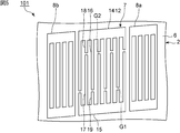
- FIG. 12 is a plan view of the elastic wave device according to the third embodiment.
- FIG. 13 is a sectional view showing the vicinity of the first gap of the IDT electrode according to the third embodiment. Note that the second dielectric film is omitted in FIG.
- FIG. 13 shows a cross section corresponding to a portion along line II in FIG.
- the first dielectric film 9a extends between the first electrode finger 16 and the second dummy electrode finger 19 and the piezoelectric substrate 2.
- the second embodiment is different from the first embodiment. More specifically, the first dielectric film 9a extends between the first electrode finger 16 and the piezoelectric substrate 2, and between the second dummy electrode finger 19 and the piezoelectric substrate 2. It has arrived. Further, the present embodiment is also different from the first embodiment in that the first dielectric film 9b extends between the second electrode finger 17 and the first dummy electrode finger 18 and the piezoelectric substrate 2. Different from Except for the above points, the elastic wave device of the present embodiment has the same configuration as the elastic wave device of the second embodiment.
- the second dielectric film 39 is formed on the piezoelectric substrate 2 so as to cover the IDT electrode 7, the first dielectric film 9a, and the first dielectric film 9b. Is provided.
- the elastic wave device having the configuration of the third embodiment and the elastic wave device of the second comparative example were manufactured.
- the acoustic wave device of the second comparative example has the same configuration as that of the third embodiment except that the first dielectric film 9a and the first dielectric film 9b are not provided.
- the conditions of the elastic wave device having the configuration of the third embodiment and the elastic wave device of the second comparative example are as follows.
- Piezoelectric layer material 50 ° YX-LiTaO 3 , film thickness 600 nm Low sonic film: Silicon oxide (SiO 2 ) material, film thickness 673 nm High sonic film: Material silicon nitride (SiN), film thickness 900nm Support substrate: Material silicon (Si), crystal orientation Si (100), Euler angle (0 °, 0 °, 45 °) Thickness of each metal layer of the IDT electrode: thickness of the Ti layer on the piezoelectric layer side is 12 nm, thickness of the Al layer is 100 nm, thickness of the Ti layer is 4 nm.
- the conditions of the first dielectric film of the acoustic wave device having the configuration of the third embodiment are as follows.
- First dielectric film Material tantalum pentoxide (Ta 2 O 5 ), film thickness 30 nm
- each acoustic wave device The impedance characteristics of each acoustic wave device are shown in FIGS. 14 and 15 below.
- FIG. 14 is a diagram showing impedance characteristics in the third embodiment and the second comparative example.
- FIG. 15 is a diagram showing impedance characteristics near the resonance frequency in the third embodiment and the second comparative example. 14 and 15, the solid line shows the result of the third embodiment, and the broken line shows the result of the second comparative example.
- ripples occur near the resonance frequency in the second comparative example.
- ripples near the resonance frequency do not occur.
- ripples near the resonance frequency can be suppressed.
- the first dielectric film 9a can be more surely covered with the first gap G1. It can be arranged to reach the whole.
- the first dielectric film 9b can be more surely arranged so as to reach the entire second gap G2. Therefore, the ripple near the resonance frequency can be suppressed more reliably and effectively.
- the resonance frequencies are similar in the third embodiment and the second comparative example.
- the anti-resonance frequency of the third embodiment is located higher than the anti-resonance frequency of the second comparative example.
- the first dielectric film 9a shown in FIG. 12 extends between the first electrode finger 16 and the second dummy electrode finger 19 and the piezoelectric substrate 2,
- the dielectric film 9b reaches between the second electrode finger 17 and the first dummy electrode finger 18 and the piezoelectric substrate 2. Thereby, the specific band can be widened.
Landscapes
- Physics & Mathematics (AREA)
- Acoustics & Sound (AREA)
- Surface Acoustic Wave Elements And Circuit Networks Thereof (AREA)
Abstract
L'invention concerne un dispositif à ondes élastiques avec lequel il est possible de réduire au minimum les ondulations au voisinage de la fréquence de résonance. L'invention concerne un dispositif à ondes élastiques 1 qui comporte un substrat piézoélectrique 2 et une électrode IDT 7 disposée sur le substrat piézoélectrique 2. Le substrat piézoélectrique 2 a une couche à vitesse acoustique élevée et une couche piézoélectrique 6. L'électrode IDT 7 comprend : une première et une seconde barre omnibus 14, 15 ; et une pluralité de premiers et seconds doigts d'électrode 16, 17 qui s'imbriquent l'un l'autre. Des première et seconde enveloppes A1, A2, qui sont des lignes imaginaires formées en reliant les extrémités respectives de la pluralité des premiers et seconds doigts d'électrode 16, 17, s'étendent de manière à être inclinées par rapport à la direction de propagation d'onde élastique. Des premiers films diélectriques 9a, 9b sont disposés sur au moins l'un d'une pluralité de premiers espaces G1 situés entre la pluralité de premiers doigts d'électrode 16 et la seconde barre omnibus 15, et une pluralité de seconds espaces G2 situés entre la pluralité de seconds doigts d'électrode 17 et la première barre omnibus 14. La densité des premiers films diélectriques 9a, 9b est supérieure à la densité d'oxyde de silicium.
Priority Applications (3)
| Application Number | Priority Date | Filing Date | Title |
|---|---|---|---|
| CN201980073441.5A CN112997403A (zh) | 2018-11-16 | 2019-11-08 | 弹性波装置 |
| JP2020555635A JPWO2020100744A1 (ja) | 2018-11-16 | 2019-11-08 | 弾性波装置 |
| US17/318,120 US20210265972A1 (en) | 2018-11-16 | 2021-05-12 | Acoustic wave device |
Applications Claiming Priority (2)
| Application Number | Priority Date | Filing Date | Title |
|---|---|---|---|
| JP2018-215573 | 2018-11-16 | ||
| JP2018215573 | 2018-11-16 |
Related Child Applications (1)
| Application Number | Title | Priority Date | Filing Date |
|---|---|---|---|
| US17/318,120 Continuation US20210265972A1 (en) | 2018-11-16 | 2021-05-12 | Acoustic wave device |
Publications (1)
| Publication Number | Publication Date |
|---|---|
| WO2020100744A1 true WO2020100744A1 (fr) | 2020-05-22 |
Family
ID=70731067
Family Applications (1)
| Application Number | Title | Priority Date | Filing Date |
|---|---|---|---|
| PCT/JP2019/043906 WO2020100744A1 (fr) | 2018-11-16 | 2019-11-08 | Dispositif à ondes élastiques |
Country Status (4)
| Country | Link |
|---|---|
| US (1) | US20210265972A1 (fr) |
| JP (1) | JPWO2020100744A1 (fr) |
| CN (1) | CN112997403A (fr) |
| WO (1) | WO2020100744A1 (fr) |
Cited By (28)
| Publication number | Priority date | Publication date | Assignee | Title |
|---|---|---|---|---|
| WO2021241364A1 (fr) * | 2020-05-27 | 2021-12-02 | 株式会社村田製作所 | Dispositif à ondes élastiques |
| JP2022540515A (ja) * | 2019-09-23 | 2022-09-15 | レゾナント インコーポレイテッド | 高出力用途のための横方向励起フィルムバルク音響共振器 |
| WO2023013741A1 (fr) * | 2021-08-04 | 2023-02-09 | 株式会社村田製作所 | Dispositif à ondes élastiques |
| WO2023085210A1 (fr) * | 2021-11-09 | 2023-05-19 | 京セラ株式会社 | Dispositif à ondes élastiques, filtre, diviseur, et dispositif de communication |
| WO2023085362A1 (fr) * | 2021-11-11 | 2023-05-19 | 株式会社村田製作所 | Dispositif à ondes élastiques |
| US11677376B2 (en) | 2018-06-15 | 2023-06-13 | Murata Manufacturing Co, Ltd. | Solidly-mounted transversely-excited film bulk acoustic resonator with recessed interdigital transducer fingers |
| US11689185B2 (en) | 2018-06-15 | 2023-06-27 | Murata Manufacturing Co., Ltd. | Solidly-mounted transversely-excited film bulk acoustic resonator with recessed interdigital transducer fingers using rotated y-x cut lithium niobate |
| US11736086B2 (en) | 2018-06-15 | 2023-08-22 | Murata Manufacturing Co., Ltd. | Filter using transversely-excited film bulk acoustic resonators with divided frequency-setting dielectric layers |
| US11817840B2 (en) | 2018-06-15 | 2023-11-14 | Murata Manufacturing Co., Ltd. | XBAR resonators with non-rectangular diaphragms |
| US11824520B2 (en) | 2018-06-15 | 2023-11-21 | Murata Manufacturing Co., Ltd. | Transversely-excited film bulk acoustic resonator with optimized electrode thickness, mark, and pitch |
| US11831289B2 (en) | 2018-06-15 | 2023-11-28 | Murata Manufacturing Co., Ltd. | Transversely-excited film bulk acoustic resonator with reduced spurious modes |
| US11870423B2 (en) | 2018-06-15 | 2024-01-09 | Murata Manufacturing Co., Ltd. | Wide bandwidth temperature-compensated transversely-excited film bulk acoustic resonator |
| US11870424B2 (en) | 2018-06-15 | 2024-01-09 | Murata Manufacturing Co., Ltd. | Filters using transversly-excited film bulk acoustic resonators with frequency-setting dielectric layers |
| US11876498B2 (en) | 2018-06-15 | 2024-01-16 | Murata Manufacturing Co., Ltd. | Transversely-excited film bulk acoustic resonator with multiple diaphragm thicknesses and fabrication method |
| US11881835B2 (en) | 2020-11-11 | 2024-01-23 | Murata Manufacturing Co., Ltd. | Transversely-excited film bulk acoustic resonator with low thermal impedance |
| US11888463B2 (en) | 2018-06-15 | 2024-01-30 | Murata Manufacturing Co., Ltd. | Multi-port filter using transversely-excited film bulk acoustic resonators |
| US11901878B2 (en) | 2018-06-15 | 2024-02-13 | Murata Manufacturing Co., Ltd. | Transversely-excited film bulk acoustic resonators with two-layer electrodes with a wider top layer |
| US11901874B2 (en) | 2018-06-15 | 2024-02-13 | Murata Manufacturing Co., Ltd. | Transversely-excited film bulk acoustic resonator with half-lambda dielectric layer |
| US11909381B2 (en) | 2018-06-15 | 2024-02-20 | Murata Manufacturing Co., Ltd. | Transversely-excited film bulk acoustic resonators with two-layer electrodes having a narrower top layer |
| US11929731B2 (en) | 2018-02-18 | 2024-03-12 | Murata Manufacturing Co., Ltd. | Transversely-excited film bulk acoustic resonator with optimized electrode mark, and pitch |
| US11936361B2 (en) | 2018-06-15 | 2024-03-19 | Murata Manufacturing Co., Ltd. | Transversely-excited film bulk acoustic resonators |
| US11949403B2 (en) | 2019-08-28 | 2024-04-02 | Murata Manufacturing Co., Ltd. | Transversely-excited film bulk acoustic resonator with interdigital transducer with varied mark and pitch |
| US11949399B2 (en) | 2018-06-15 | 2024-04-02 | Murata Manufacturing Co., Ltd. | Solidly-mounted transversely-excited film bulk acoustic resonator with diamond layers in Bragg reflector stack |
| US11967946B2 (en) | 2020-02-18 | 2024-04-23 | Murata Manufacturing Co., Ltd. | Transversely-excited film bulk acoustic resonator with a bonding layer and an etch-stop layer |
| US11984868B2 (en) | 2018-06-15 | 2024-05-14 | Murata Manufacturing Co., Ltd. | Filter using piezoelectric film bonded to high resistivity silicon substrate with trap-rich layer |
| US11984872B2 (en) | 2018-06-15 | 2024-05-14 | Murata Manufacturing Co., Ltd. | Film bulk acoustic resonator fabrication method |
| US11990888B2 (en) | 2018-06-15 | 2024-05-21 | Murata Manufacturing Co., Ltd. | Resonator using YX-cut lithium niobate for high power applications |
| US11996822B2 (en) | 2020-12-01 | 2024-05-28 | Murata Manufacturing Co., Ltd. | Wide bandwidth time division duplex transceiver |
Families Citing this family (2)
| Publication number | Priority date | Publication date | Assignee | Title |
|---|---|---|---|---|
| DE102018131952A1 (de) * | 2018-12-12 | 2020-06-18 | RF360 Europe GmbH | Elektroakustischer Resonator mit unterdrückter Anregungtransversaler Spaltmoden und verringerten transversalen Moden |
| WO2024027920A1 (fr) * | 2022-08-05 | 2024-02-08 | Huawei Technologies Co., Ltd. | Procédé de fabrication d'un résonateur à ondes acoustiques de surface |
Citations (8)
| Publication number | Priority date | Publication date | Assignee | Title |
|---|---|---|---|---|
| WO2008126614A1 (fr) * | 2007-03-27 | 2008-10-23 | Murata Manufacturing Co., Ltd. | Dispositif à onde élastique |
| JP2009290472A (ja) * | 2008-05-28 | 2009-12-10 | Fujitsu Ltd | 弾性波デバイス、フィルタ、通信モジュール、および通信装置 |
| WO2011142183A1 (fr) * | 2010-05-10 | 2011-11-17 | 株式会社村田製作所 | Dispositif à ondes acoustiques de surface |
| WO2012090873A1 (fr) * | 2010-12-28 | 2012-07-05 | 京セラ株式会社 | Élément à ondes élastiques et dispositif à ondes élastiques utilisant celui-ci |
| WO2012127793A1 (fr) * | 2011-03-22 | 2012-09-27 | パナソニック株式会社 | Élément à onde élastique |
| JP2015109574A (ja) * | 2013-12-05 | 2015-06-11 | 株式会社村田製作所 | 縦結合共振子型弾性表面波フィルタおよび通信機 |
| WO2016208446A1 (fr) * | 2015-06-24 | 2016-12-29 | 株式会社村田製作所 | Dispositif de filtre |
| WO2018117060A1 (fr) * | 2016-12-19 | 2018-06-28 | 株式会社村田製作所 | Résonateur à ondes acoustiques, dispositif de filtre et multiplexeur |
Family Cites Families (5)
| Publication number | Priority date | Publication date | Assignee | Title |
|---|---|---|---|---|
| DE102010005596B4 (de) * | 2010-01-25 | 2015-11-05 | Epcos Ag | Elektroakustischer Wandler mit verringerten Verlusten durch transversale Emission und verbesserter Performance durch Unterdrückung transversaler Moden |
| JP2011182220A (ja) * | 2010-03-02 | 2011-09-15 | Panasonic Corp | 弾性波共振器及びこれを用いた縦結合二重モードフィルタ、ラダー型フィルタ |
| WO2013172251A1 (fr) * | 2012-05-17 | 2013-11-21 | 株式会社村田製作所 | Appareil à ondes acoustiques de surface |
| WO2018003273A1 (fr) * | 2016-06-28 | 2018-01-04 | 株式会社村田製作所 | Multiplexeur, circuit frontal à haute fréquence et dispositif de communication |
| DE102016118124B4 (de) * | 2016-09-26 | 2023-11-30 | Snaptrack, Inc. | Elektroakustischer Wandler mit verbesserter ESD Festigkeit |
-
2019
- 2019-11-08 CN CN201980073441.5A patent/CN112997403A/zh active Pending
- 2019-11-08 JP JP2020555635A patent/JPWO2020100744A1/ja active Pending
- 2019-11-08 WO PCT/JP2019/043906 patent/WO2020100744A1/fr active Application Filing
-
2021
- 2021-05-12 US US17/318,120 patent/US20210265972A1/en active Pending
Patent Citations (8)
| Publication number | Priority date | Publication date | Assignee | Title |
|---|---|---|---|---|
| WO2008126614A1 (fr) * | 2007-03-27 | 2008-10-23 | Murata Manufacturing Co., Ltd. | Dispositif à onde élastique |
| JP2009290472A (ja) * | 2008-05-28 | 2009-12-10 | Fujitsu Ltd | 弾性波デバイス、フィルタ、通信モジュール、および通信装置 |
| WO2011142183A1 (fr) * | 2010-05-10 | 2011-11-17 | 株式会社村田製作所 | Dispositif à ondes acoustiques de surface |
| WO2012090873A1 (fr) * | 2010-12-28 | 2012-07-05 | 京セラ株式会社 | Élément à ondes élastiques et dispositif à ondes élastiques utilisant celui-ci |
| WO2012127793A1 (fr) * | 2011-03-22 | 2012-09-27 | パナソニック株式会社 | Élément à onde élastique |
| JP2015109574A (ja) * | 2013-12-05 | 2015-06-11 | 株式会社村田製作所 | 縦結合共振子型弾性表面波フィルタおよび通信機 |
| WO2016208446A1 (fr) * | 2015-06-24 | 2016-12-29 | 株式会社村田製作所 | Dispositif de filtre |
| WO2018117060A1 (fr) * | 2016-12-19 | 2018-06-28 | 株式会社村田製作所 | Résonateur à ondes acoustiques, dispositif de filtre et multiplexeur |
Cited By (39)
| Publication number | Priority date | Publication date | Assignee | Title |
|---|---|---|---|---|
| US11929731B2 (en) | 2018-02-18 | 2024-03-12 | Murata Manufacturing Co., Ltd. | Transversely-excited film bulk acoustic resonator with optimized electrode mark, and pitch |
| US11901878B2 (en) | 2018-06-15 | 2024-02-13 | Murata Manufacturing Co., Ltd. | Transversely-excited film bulk acoustic resonators with two-layer electrodes with a wider top layer |
| US11949399B2 (en) | 2018-06-15 | 2024-04-02 | Murata Manufacturing Co., Ltd. | Solidly-mounted transversely-excited film bulk acoustic resonator with diamond layers in Bragg reflector stack |
| US11909381B2 (en) | 2018-06-15 | 2024-02-20 | Murata Manufacturing Co., Ltd. | Transversely-excited film bulk acoustic resonators with two-layer electrodes having a narrower top layer |
| US11990888B2 (en) | 2018-06-15 | 2024-05-21 | Murata Manufacturing Co., Ltd. | Resonator using YX-cut lithium niobate for high power applications |
| US11677376B2 (en) | 2018-06-15 | 2023-06-13 | Murata Manufacturing Co, Ltd. | Solidly-mounted transversely-excited film bulk acoustic resonator with recessed interdigital transducer fingers |
| US11689185B2 (en) | 2018-06-15 | 2023-06-27 | Murata Manufacturing Co., Ltd. | Solidly-mounted transversely-excited film bulk acoustic resonator with recessed interdigital transducer fingers using rotated y-x cut lithium niobate |
| US11736086B2 (en) | 2018-06-15 | 2023-08-22 | Murata Manufacturing Co., Ltd. | Filter using transversely-excited film bulk acoustic resonators with divided frequency-setting dielectric layers |
| US11817840B2 (en) | 2018-06-15 | 2023-11-14 | Murata Manufacturing Co., Ltd. | XBAR resonators with non-rectangular diaphragms |
| US11901874B2 (en) | 2018-06-15 | 2024-02-13 | Murata Manufacturing Co., Ltd. | Transversely-excited film bulk acoustic resonator with half-lambda dielectric layer |
| US11831289B2 (en) | 2018-06-15 | 2023-11-28 | Murata Manufacturing Co., Ltd. | Transversely-excited film bulk acoustic resonator with reduced spurious modes |
| US11870423B2 (en) | 2018-06-15 | 2024-01-09 | Murata Manufacturing Co., Ltd. | Wide bandwidth temperature-compensated transversely-excited film bulk acoustic resonator |
| US11870424B2 (en) | 2018-06-15 | 2024-01-09 | Murata Manufacturing Co., Ltd. | Filters using transversly-excited film bulk acoustic resonators with frequency-setting dielectric layers |
| US11876498B2 (en) | 2018-06-15 | 2024-01-16 | Murata Manufacturing Co., Ltd. | Transversely-excited film bulk acoustic resonator with multiple diaphragm thicknesses and fabrication method |
| US11984872B2 (en) | 2018-06-15 | 2024-05-14 | Murata Manufacturing Co., Ltd. | Film bulk acoustic resonator fabrication method |
| US11881834B2 (en) | 2018-06-15 | 2024-01-23 | Murata Manufacturing Co., Ltd. | Transversely-excited film bulk acoustic resonator with reduced spurious modes |
| US11888465B2 (en) | 2018-06-15 | 2024-01-30 | Murata Manufacturing Co., Ltd. | Bandpass filter with frequency separation between shunt and series resonators set by dielectric layer thickness |
| US11888463B2 (en) | 2018-06-15 | 2024-01-30 | Murata Manufacturing Co., Ltd. | Multi-port filter using transversely-excited film bulk acoustic resonators |
| US11984868B2 (en) | 2018-06-15 | 2024-05-14 | Murata Manufacturing Co., Ltd. | Filter using piezoelectric film bonded to high resistivity silicon substrate with trap-rich layer |
| US11824520B2 (en) | 2018-06-15 | 2023-11-21 | Murata Manufacturing Co., Ltd. | Transversely-excited film bulk acoustic resonator with optimized electrode thickness, mark, and pitch |
| US11967945B2 (en) | 2018-06-15 | 2024-04-23 | Murata Manufacturing Co., Ltd. | Transversly-excited film bulk acoustic resonators and filters |
| US11942922B2 (en) | 2018-06-15 | 2024-03-26 | Murata Manufacturing Co., Ltd. | Transversely-excited film bulk acoustic resonator with optimized electrode thickness, mark, and pitch |
| US11929735B2 (en) | 2018-06-15 | 2024-03-12 | Murata Manufacturing Co., Ltd. | XBAR resonators with non-rectangular diaphragms |
| US11929727B2 (en) | 2018-06-15 | 2024-03-12 | Murata Manufacturing Co., Ltd. | Transversely-excited film bulk acoustic resonator with reduced spurious modes |
| US11923821B2 (en) | 2018-06-15 | 2024-03-05 | Murata Manufacturing Co., Ltd. | Transversely-excited film bulk acoustic resonator with reduced spurious modes |
| US11936361B2 (en) | 2018-06-15 | 2024-03-19 | Murata Manufacturing Co., Ltd. | Transversely-excited film bulk acoustic resonators |
| US11949403B2 (en) | 2019-08-28 | 2024-04-02 | Murata Manufacturing Co., Ltd. | Transversely-excited film bulk acoustic resonator with interdigital transducer with varied mark and pitch |
| JP2022540515A (ja) * | 2019-09-23 | 2022-09-15 | レゾナント インコーポレイテッド | 高出力用途のための横方向励起フィルムバルク音響共振器 |
| US11967946B2 (en) | 2020-02-18 | 2024-04-23 | Murata Manufacturing Co., Ltd. | Transversely-excited film bulk acoustic resonator with a bonding layer and an etch-stop layer |
| WO2021241364A1 (fr) * | 2020-05-27 | 2021-12-02 | 株式会社村田製作所 | Dispositif à ondes élastiques |
| JP7464116B2 (ja) | 2020-05-27 | 2024-04-09 | 株式会社村田製作所 | 弾性波装置 |
| US11936358B2 (en) | 2020-11-11 | 2024-03-19 | Murata Manufacturing Co., Ltd. | Transversely-excited film bulk acoustic resonator with low thermal impedance |
| US11881835B2 (en) | 2020-11-11 | 2024-01-23 | Murata Manufacturing Co., Ltd. | Transversely-excited film bulk acoustic resonator with low thermal impedance |
| US11996822B2 (en) | 2020-12-01 | 2024-05-28 | Murata Manufacturing Co., Ltd. | Wide bandwidth time division duplex transceiver |
| US11996826B2 (en) | 2020-12-08 | 2024-05-28 | Murata Manufacturing Co., Ltd. | Transversely-excited film bulk acoustic resonator with thermally conductive etch-stop layer |
| US11996827B2 (en) | 2021-02-05 | 2024-05-28 | Murata Manufacturing Co., Ltd. | Transversely-excited film bulk acoustic resonator with periodic etched holes |
| WO2023013741A1 (fr) * | 2021-08-04 | 2023-02-09 | 株式会社村田製作所 | Dispositif à ondes élastiques |
| WO2023085210A1 (fr) * | 2021-11-09 | 2023-05-19 | 京セラ株式会社 | Dispositif à ondes élastiques, filtre, diviseur, et dispositif de communication |
| WO2023085362A1 (fr) * | 2021-11-11 | 2023-05-19 | 株式会社村田製作所 | Dispositif à ondes élastiques |
Also Published As
| Publication number | Publication date |
|---|---|
| CN112997403A (zh) | 2021-06-18 |
| JPWO2020100744A1 (ja) | 2021-09-27 |
| US20210265972A1 (en) | 2021-08-26 |
Similar Documents
| Publication | Publication Date | Title |
|---|---|---|
| WO2020100744A1 (fr) | Dispositif à ondes élastiques | |
| US11444601B2 (en) | Acoustic wave device | |
| WO2020171050A1 (fr) | Dispositif à ondes élastiques | |
| US20220224311A1 (en) | Acoustic wave device | |
| JP7268747B2 (ja) | 弾性波装置 | |
| US11456719B2 (en) | Acoustic wave device | |
| US11146237B2 (en) | Acoustic wave device | |
| US20240154595A1 (en) | Acoustic wave device | |
| CN213783263U (zh) | 弹性波装置 | |
| US20230327634A1 (en) | Acoustic wave device | |
| US20230155569A1 (en) | Acoustic wave device | |
| US20230037955A1 (en) | Acoustic wave device | |
| CN113454912A (zh) | 弹性波装置 | |
| WO2021220936A1 (fr) | Dispositif à ondes élastiques | |
| WO2022019169A1 (fr) | Filtre de type échelle | |
| CN212463171U (zh) | 弹性波装置 | |
| WO2024029361A1 (fr) | Dispositif à ondes élastiques et dispositif de filtre | |
| WO2023234321A1 (fr) | Dispositif à ondes élastiques | |
| US20230107416A1 (en) | Acoustic wave device | |
| WO2020241776A1 (fr) | Dispositif à ondes élastiques | |
| WO2020080463A1 (fr) | Dispositif à ondes élastiques, filtre passe-bande, duplexeur et multiplexeur | |
| WO2022158363A1 (fr) | Dispositif à ondes élastiques | |
| WO2022025040A1 (fr) | Dispositif à ondes élastiques | |
| WO2024009660A1 (fr) | Dispositif à ondes élastiques et dispositif de filtre | |
| CN116458062A (zh) | 弹性波装置 |
Legal Events
| Date | Code | Title | Description |
|---|---|---|---|
| 121 | Ep: the epo has been informed by wipo that ep was designated in this application |
Ref document number: 19884341 Country of ref document: EP Kind code of ref document: A1 |
|
| ENP | Entry into the national phase |
Ref document number: 2020555635 Country of ref document: JP Kind code of ref document: A |
|
| NENP | Non-entry into the national phase |
Ref country code: DE |
|
| 122 | Ep: pct application non-entry in european phase |
Ref document number: 19884341 Country of ref document: EP Kind code of ref document: A1 |