WO2023085033A1 - 半導体装置 - Google Patents
半導体装置 Download PDFInfo
- Publication number
- WO2023085033A1 WO2023085033A1 PCT/JP2022/039095 JP2022039095W WO2023085033A1 WO 2023085033 A1 WO2023085033 A1 WO 2023085033A1 JP 2022039095 W JP2022039095 W JP 2022039095W WO 2023085033 A1 WO2023085033 A1 WO 2023085033A1
- Authority
- WO
- WIPO (PCT)
- Prior art keywords
- terminals
- semiconductor device
- terminal
- dimension
- sealing resin
- Prior art date
- Legal status (The legal status is an assumption and is not a legal conclusion. Google has not performed a legal analysis and makes no representation as to the accuracy of the status listed.)
- Ceased
Links
Images


Classifications
-
- H—ELECTRICITY
- H10—SEMICONDUCTOR DEVICES; ELECTRIC SOLID-STATE DEVICES NOT OTHERWISE PROVIDED FOR
- H10W—GENERIC PACKAGES, INTERCONNECTIONS, CONNECTORS OR OTHER CONSTRUCTIONAL DETAILS OF DEVICES COVERED BY CLASS H10
- H10W70/00—Package substrates; Interposers; Redistribution layers [RDL]
- H10W70/01—Manufacture or treatment
- H10W70/04—Manufacture or treatment of leadframes
- H10W70/048—Mechanical treatments, e.g. punching, cutting, deforming or cold welding
-
- H—ELECTRICITY
- H10—SEMICONDUCTOR DEVICES; ELECTRIC SOLID-STATE DEVICES NOT OTHERWISE PROVIDED FOR
- H10W—GENERIC PACKAGES, INTERCONNECTIONS, CONNECTORS OR OTHER CONSTRUCTIONAL DETAILS OF DEVICES COVERED BY CLASS H10
- H10W70/00—Package substrates; Interposers; Redistribution layers [RDL]
- H10W70/40—Leadframes
- H10W70/411—Chip-supporting parts, e.g. die pads
- H10W70/417—Bonding materials between chips and die pads
-
- H—ELECTRICITY
- H10—SEMICONDUCTOR DEVICES; ELECTRIC SOLID-STATE DEVICES NOT OTHERWISE PROVIDED FOR
- H10W—GENERIC PACKAGES, INTERCONNECTIONS, CONNECTORS OR OTHER CONSTRUCTIONAL DETAILS OF DEVICES COVERED BY CLASS H10
- H10W70/00—Package substrates; Interposers; Redistribution layers [RDL]
- H10W70/40—Leadframes
- H10W70/421—Shapes or dispositions
- H10W70/424—Cross-sectional shapes
-
- H—ELECTRICITY
- H10—SEMICONDUCTOR DEVICES; ELECTRIC SOLID-STATE DEVICES NOT OTHERWISE PROVIDED FOR
- H10W—GENERIC PACKAGES, INTERCONNECTIONS, CONNECTORS OR OTHER CONSTRUCTIONAL DETAILS OF DEVICES COVERED BY CLASS H10
- H10W70/00—Package substrates; Interposers; Redistribution layers [RDL]
- H10W70/40—Leadframes
- H10W70/456—Materials
- H10W70/457—Materials of metallic layers on leadframes
-
- H—ELECTRICITY
- H10—SEMICONDUCTOR DEVICES; ELECTRIC SOLID-STATE DEVICES NOT OTHERWISE PROVIDED FOR
- H10W—GENERIC PACKAGES, INTERCONNECTIONS, CONNECTORS OR OTHER CONSTRUCTIONAL DETAILS OF DEVICES COVERED BY CLASS H10
- H10W72/00—Interconnections or connectors in packages
-
- H—ELECTRICITY
- H10—SEMICONDUCTOR DEVICES; ELECTRIC SOLID-STATE DEVICES NOT OTHERWISE PROVIDED FOR
- H10W—GENERIC PACKAGES, INTERCONNECTIONS, CONNECTORS OR OTHER CONSTRUCTIONAL DETAILS OF DEVICES COVERED BY CLASS H10
- H10W72/00—Interconnections or connectors in packages
- H10W72/071—Connecting or disconnecting
- H10W72/075—Connecting or disconnecting of bond wires
-
- H—ELECTRICITY
- H10—SEMICONDUCTOR DEVICES; ELECTRIC SOLID-STATE DEVICES NOT OTHERWISE PROVIDED FOR
- H10W—GENERIC PACKAGES, INTERCONNECTIONS, CONNECTORS OR OTHER CONSTRUCTIONAL DETAILS OF DEVICES COVERED BY CLASS H10
- H10W72/00—Interconnections or connectors in packages
- H10W72/50—Bond wires
-
- H—ELECTRICITY
- H10—SEMICONDUCTOR DEVICES; ELECTRIC SOLID-STATE DEVICES NOT OTHERWISE PROVIDED FOR
- H10W—GENERIC PACKAGES, INTERCONNECTIONS, CONNECTORS OR OTHER CONSTRUCTIONAL DETAILS OF DEVICES COVERED BY CLASS H10
- H10W74/00—Encapsulations, e.g. protective coatings
- H10W74/01—Manufacture or treatment
- H10W74/014—Manufacture or treatment using batch processing
-
- H—ELECTRICITY
- H10—SEMICONDUCTOR DEVICES; ELECTRIC SOLID-STATE DEVICES NOT OTHERWISE PROVIDED FOR
- H10W—GENERIC PACKAGES, INTERCONNECTIONS, CONNECTORS OR OTHER CONSTRUCTIONAL DETAILS OF DEVICES COVERED BY CLASS H10
- H10W74/00—Encapsulations, e.g. protective coatings
- H10W74/10—Encapsulations, e.g. protective coatings characterised by their shape or disposition
- H10W74/111—Encapsulations, e.g. protective coatings characterised by their shape or disposition the semiconductor body being completely enclosed
-
- H—ELECTRICITY
- H10—SEMICONDUCTOR DEVICES; ELECTRIC SOLID-STATE DEVICES NOT OTHERWISE PROVIDED FOR
- H10W—GENERIC PACKAGES, INTERCONNECTIONS, CONNECTORS OR OTHER CONSTRUCTIONAL DETAILS OF DEVICES COVERED BY CLASS H10
- H10W70/00—Package substrates; Interposers; Redistribution layers [RDL]
- H10W70/40—Leadframes
- H10W70/421—Shapes or dispositions
-
- H—ELECTRICITY
- H10—SEMICONDUCTOR DEVICES; ELECTRIC SOLID-STATE DEVICES NOT OTHERWISE PROVIDED FOR
- H10W—GENERIC PACKAGES, INTERCONNECTIONS, CONNECTORS OR OTHER CONSTRUCTIONAL DETAILS OF DEVICES COVERED BY CLASS H10
- H10W70/00—Package substrates; Interposers; Redistribution layers [RDL]
- H10W70/40—Leadframes
- H10W70/456—Materials
-
- H—ELECTRICITY
- H10—SEMICONDUCTOR DEVICES; ELECTRIC SOLID-STATE DEVICES NOT OTHERWISE PROVIDED FOR
- H10W—GENERIC PACKAGES, INTERCONNECTIONS, CONNECTORS OR OTHER CONSTRUCTIONAL DETAILS OF DEVICES COVERED BY CLASS H10
- H10W90/00—Package configurations
- H10W90/701—Package configurations characterised by the relative positions of pads or connectors relative to package parts
- H10W90/751—Package configurations characterised by the relative positions of pads or connectors relative to package parts of bond wires
- H10W90/756—Package configurations characterised by the relative positions of pads or connectors relative to package parts of bond wires between a chip and a stacked lead frame, conducting package substrate or heat sink
Definitions
- the present disclosure relates to semiconductor devices.
- Patent Document 1 describes a plurality of terminals arranged along a predetermined direction, a semiconductor element electrically connected to at least one of the plurality of terminals, and a sealing device covering a part of each of the plurality of terminals and the semiconductor element.
- An example of a semiconductor device comprising a resin is disclosed.
- Each terminal has a terminal rear surface and a terminal outer surface exposed from the sealing resin.
- a similar solder fillet is formed on the terminal outer surface of each of the plurality of terminals.
- solder fillet contributes to improving the bonding strength of the semiconductor device to the wiring board.
- thermal stress of different magnitudes may act on each of the plurality of terminals.
- solder fillets formed on certain terminals may crack.
- An object of the present disclosure is to provide an improved semiconductor device.
- an object of the present disclosure is to provide a semiconductor device capable of having different heights of solder fillets formed on each of a plurality of terminals when mounted on a wiring board.
- a semiconductor device provided by the present disclosure includes: a plurality of terminals arranged along a first direction orthogonal to a thickness direction; a semiconductor element electrically connected to at least one of the plurality of terminals; A sealing resin covering a portion of each of the terminals and the semiconductor element is provided.
- Each of the plurality of terminals has a mounting surface and a side surface connected to the mounting surface.
- the mounting surface faces the thickness direction and is exposed from the sealing resin
- the side surface faces the thickness direction and a second direction orthogonal to the first direction and faces the sealing resin. It is exposed from the stopping resin.
- the plurality of terminals includes a first terminal located closest to one end of the sealing resin in the first direction, and a second terminal located away from the first terminal.
- the side surfaces of the plurality of terminals include a first side surface of the first terminal and a second side surface of the second terminal. A second dimension in the thickness direction of the second side surface is different from a first dimension in the thickness direction of the first side surface.
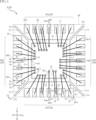
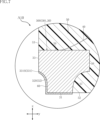
- FIG. 1 is a plan view of a semiconductor device according to a first embodiment of the present disclosure, which is transparent through a sealing resin.
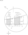
- 2 is a bottom view of the semiconductor device shown in FIG. 1.
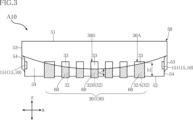
- FIG. 3 is a front view of the semiconductor device shown in FIG. 1.
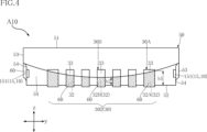
- FIG. 4 is a left side view of the semiconductor device shown in FIG. 1.
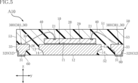
- FIG. 5 is a cross-sectional view along line VV of FIG.
- FIG. 6 is a cross-sectional view along line VI-VI of FIG. 7 is a partially enlarged view of FIG. 5.
- FIG. FIG. 8 is a partially enlarged view of the first terminal shown in FIG. 3 and its vicinity.
- FIG. 9 is a partially enlarged view of the second terminal shown in FIG. 3 and its vicinity.
- FIG. 10A to 10D are cross-sectional views for explaining the manufacturing process of the semiconductor device shown in FIG. 11A and 11B are cross-sectional views for explaining the manufacturing process of the semiconductor device shown in FIG. 12A and 12B are cross-sectional views for explaining the manufacturing process of the semiconductor device shown in FIG. 13A to 13C are cross-sectional views for explaining the manufacturing process of the semiconductor device shown in FIG.
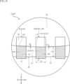
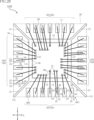
- FIG. 14 is a plan view of the semiconductor device according to the second embodiment of the present disclosure, which is transparent through the sealing resin.
- 15 is a front view of the semiconductor device shown in FIG. 14.
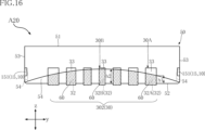
- FIG. 16 is a left side view of the semiconductor device shown in FIG. 14.
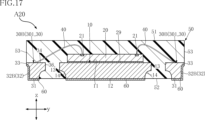
- FIG. 17 is a cross-sectional view along line XVII-XVII of FIG. 14.
- FIG. 15 is a front view of the semiconductor device shown in FIG. 14.
- FIG. 16 is a left side view of the semiconductor device shown in FIG. 14.
- FIG. 17 is a cross-sectional view along line XVII-X
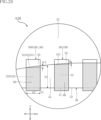
- FIG. 18 is a partially enlarged view of the first terminal and its vicinity shown in FIG. 15.
- FIG. 19 is a partially enlarged view of the second terminal and its vicinity shown in FIG. 15.
- FIG. FIG. 20 is a plan view of the semiconductor device according to the third embodiment of the present disclosure, which is transparent through the sealing resin.
- 21 is a front view of the semiconductor device shown in FIG. 20.
- FIG. 22 is a left side view of the semiconductor device shown in FIG. 20.
- FIG. FIG. 23 is a partially enlarged view of the first terminal shown in FIG. 21 and its vicinity.
- FIG. 24 is a partially enlarged view of the second terminal shown in FIG. 21 and its vicinity.
- a semiconductor device A10 according to the first embodiment of the present disclosure will be described based on FIGS. 1 to 9.
- FIG. The semiconductor device A10 is surface-mounted on circuit boards of various electronic devices.
- the package format of the semiconductor device A10 is a QFN (Quad Flat Non-leaded package).
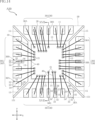
- a semiconductor device A10 includes a die pad 10, a semiconductor element 20, a plurality of terminals 30, a plurality of wires 40, and a sealing resin 50.
- FIG. 1 is transparent through the sealing resin 50 for convenience of understanding.
- the permeated sealing resin 50 is indicated by an imaginary line (chain double-dashed line).
- the covering layer 60 is indicated by a plurality of points.
- the thickness direction of each terminal 30 (or the die pad 10, the semiconductor element 20, etc.) will be referred to as the "thickness direction z".
- a direction perpendicular to the thickness direction z is called a “first direction x”.
- a direction orthogonal to both the thickness direction z and the first direction x is called a “second direction y”.
- the sealing resin 50 covers the semiconductor element 20 and part of each of the die pad 10 and the plurality of terminals 30, as shown in FIG.
- the sealing resin 50 has electrical insulation.
- Sealing resin 50 includes, for example, black epoxy resin.
- the sealing resin 50 has a top surface 51, a bottom surface 52, a first side surface 53 and a second side surface .
- the top surface 51 faces one side in the thickness direction z.
- the bottom surface 52 faces away from the top surface 51 in the thickness direction z.
- the first side surface 53 faces a direction perpendicular to the thickness direction z and is connected to the top surface 51.
- the first side surface 53 includes two regions facing the first direction x (more precisely, two regions facing opposite sides in the first direction x; the same applies hereinafter) and a second direction y and two regions facing the
- the second side surface 54 is oriented perpendicular to the thickness direction z and connected to the bottom surface 52 and the first side surface 53 .
- the second side surface 54 includes two regions facing the first direction x and two regions facing the second direction y.
- the second side surface 54 When viewed in the thickness direction z, the second side surface 54 is located inside the sealing resin 50 (closer to the semiconductor element 20 ) than the first side surface 53 . As shown in FIGS. 3 and 4, when viewed in the second direction y and the first direction x, the boundary line between the first side surface 53 and the second side surface 54 of the sealing resin 50 extends toward the bottom surface 52. Overlap arcs that are convex.
- the die pad 10 is located away from the plurality of terminals 30, as shown in FIGS.
- Die pad 10 contains a metal element.
- the metal element is, for example, copper (Cu).
- the die pad 10 and the plurality of terminals 30 are obtained from the same leadframe.
- the die pad 10 has a mounting surface 11 , a back surface 12 , a peripheral surface 13 , a peripheral groove 14 and a plurality of hangers 15 .
- the mounting surface 11 faces the same side as the top surface 51 of the sealing resin 50 in the thickness direction z.
- the mounting surface 11 faces the semiconductor element 20 .
- the rear surface 12 faces the side opposite to the mounting surface 11 in the thickness direction z.
- Back surface 12 is exposed from bottom surface 52 of sealing resin 50 .
- the area of the back surface 12 is smaller than the area of the mounting surface 11 .
- the peripheral surface 13 is oriented in a direction perpendicular to the thickness direction z and connected to the mounting surface 11. As shown in FIGS. The peripheral surface 13 surrounds the back surface 12 when viewed in the thickness direction z. As shown in FIGS. 1 and 5 , circumferential groove 14 is recessed inwardly of die pad 10 from rear surface 12 and circumferential surface 13 . The circumferential groove 14 surrounds the back surface 12 when viewed in the thickness direction z. The circumferential groove 14 is in contact with the sealing resin 50 .
- each hanger 15 radially extend from the four corners of the mounting surface 11 when viewed in the thickness direction z.
- each hanger 15 is flush with the mounting surface 11 .
- a plurality of hangers 15 are used to connect the die pad 10 to the lead frame.
- the dimension of each hanging portion 15 in the thickness direction z is smaller than the distance in the thickness direction z from the mounting surface 11 to the back surface 12 .
- each hanger 15 has an end face 151 facing in a first direction x and a second direction y. More precisely, each end face 151 has a region facing the first direction x and a region facing the second direction y.
- Each end surface 151 is exposed from the second side surface 54 of the sealing resin 50 (see FIGS. 3 and 4).
- the semiconductor element 20 is mounted on the mounting surface 11 of the die pad 10, as shown in FIGS.
- the semiconductor element 20 is an integrated circuit (IC) including a driving circuit for lighting a light source such as an LED.
- IC integrated circuit
- a semiconductor element 20 has a plurality of electrodes 21 .
- the plurality of electrodes 21 are provided on one side of the semiconductor element 20 in the thickness direction z.
- the plurality of electrodes 21 are electrically connected to a circuit configured inside the semiconductor element 20 .
- a composition of the plurality of electrodes 21 includes, for example, aluminum (Al).
- each electrode 21 is electrically connected to at least one of the terminals 30 .
- the bonding layer 29 is interposed between the mounting surface 11 of the die pad 10 and the semiconductor element 20, as shown in FIG.
- the bonding layer 29 is made of, for example, a paste containing silver-containing epoxy resin as a main component (so-called Ag paste).
- the semiconductor element 20 is bonded to the mounting surface 11 via the bonding layer 29 .
- the plurality of terminals 30 includes two first terminal groups 301 and two second terminal groups 302, as shown in FIGS.
- the two first terminal groups 301 are positioned apart from each other in the second direction y, and the plurality of terminals 30 belonging to each terminal group are arranged along the first direction x.
- the two second terminal groups 302 are separated from each other in the first direction x, and the terminals 30 belonging to each terminal group are arranged along the second direction y.
- Each of the two first terminal groups 301 and the two second terminal groups 302 includes one first terminal 30A and one second terminal 30B.
- the configuration of the plurality of terminals 30 is the same in each of these groups. Therefore, the configuration of the plurality of terminals 30 will be described using one of the two first terminal groups 301 as a representative.
- each of the plurality of terminals 30 has a mounting surface 31, a side surface 32, an end surface 33, a connecting surface 34, an inner surface 35, an inner end surface 36 and a curved surface 37.
- the mounting surface 31 faces the same side as the back surface 12 of the die pad 10 in the thickness direction z.
- the mounting surface 31 is exposed from the bottom surface 52 of the sealing resin 50 .
- the mounting surface 31 faces the wiring board.
- the side surface 32 faces the second direction y and is connected to the mounting surface 31. As shown in FIGS. The side surface 32 is exposed from the second side surface 54 of the sealing resin 50 .
- the side surfaces 32 of the terminals 30 include a first side surface 32A and a second side surface 32B.
- the first side surface 32A corresponds to the side surface 32 of the first terminal 30A.
- the second side surface 32B corresponds to the side surface 32 of the second terminal 30B.
- a second dimension h2 in the thickness direction z of the second side surface 32B is different from a first dimension h1 in the thickness direction z of the first side surface 32A.
- the first dimension h1 is the maximum value of the dimension in the thickness direction z of the first side surface 32A.
- the second dimension h2 is the maximum dimension of the second side surface 32B in the thickness direction z.
- the second dimension h2 is smaller than the first dimension h1.
- the first dimension h1 is the largest.
- the dimension in the thickness direction z of each of the side surfaces 32 of the plurality of terminals 30 positioned between the first terminal 30A and the second terminal 30B is is smaller than the first dimension h1 and larger than the second dimension h2.
- the dimension of the side surface 32 in the thickness direction z gradually decreases from the first terminal 30A to the second terminal 30B.
- the dimension b1 of the first side surface 32A in the first direction x is greater than the dimension b2 of the second side surface 32B in the first direction x.
- the end surface 33 faces the second direction y and is connected to the side surface 32.
- the end surface 33 is located on the opposite side of the mounting surface 31 with respect to the side surface 32 in each of the thickness direction z and the second direction y.
- the end surface 33 is exposed from the first side surface 53 of the sealing resin 50 .
- each of the terminals 30 has a boundary line 331 between the side surface 32 and the end surface 33 .
- Boundary lines 331 of the terminals 30 include a first boundary line 331A and a second boundary line 331B.
- the first boundary line 331A is the boundary line 331 of the first terminal 30A.
- a second boundary line 331B is the boundary line 331 of the second terminal 30B.
- the first boundary line 331A is inclined with respect to the first direction x.
- the second boundary line 331B is inclined with respect to the first direction x.
- the inclination angle ⁇ 2 (FIG. 9) of the second boundary line 331B with respect to the first direction x is smaller than the inclination angle ⁇ 1 (FIG.
- the tilt angle ⁇ (including the tilt angle ⁇ 1 and the tilt angle ⁇ 2) is given, for example, as the maximum acute angle among the intersection angles between the straight line extending along the first direction x and the tangent to the boundary line 331.
- the inclination angle ⁇ for each terminal may be the minimum acute angle (or intermediate value) of the crossing angles between the straight line extending along the first direction x and the tangent to the boundary line 331 .
- connection surface 34 faces the side opposite to the mounting surface 31 in the thickness direction z.
- the connecting surface 34 is connected to the end surface 33 .
- the area of the connection surface 34 is larger than the area of the mounting surface 31 .
- the inner side surface 35 faces the first direction x and is connected to the mounting surface 31 and the connecting surface 34 .
- the inner surface 35 includes two regions spaced apart from each other in the first direction x.
- the inner side surface 35 is in contact with the sealing resin 50 .
- the inner end surface 36 faces the opposite side of the end surface 33 in the second direction y.
- the inner end surface 36 is connected to the connecting surface 34 and the inner surface 35 .
- the areas of the inner end surfaces 36 of the terminals 30 are equal to each other.
- the inner end face 36 is in contact with the sealing resin 50 .
- the curved surface 37 is connected to the mounting surface 31, the inner surface 35 and the inner end surface 36, and curves toward the inside of any one of the terminals 30. .
- the curved surface 37 overlaps the connecting surface 34 when viewed in the thickness direction z.
- the curved surface 37 is in contact with the sealing resin 50 .
- Each of the plurality of wires 40 is conductively joined to any of the plurality of electrodes 21 of the semiconductor element 20 and any of the connection surfaces 34 of the plurality of terminals 30, as shown in FIGS. Thereby, the semiconductor element 20 is electrically connected to at least one of the plurality of terminals 30 .
- the composition of the plurality of wires 40 includes gold (Au), for example.
- the covering layer 60 covers the mounting surfaces 31 and side surfaces 32 of the terminals 30, as shown in FIGS.
- the coating layer 60 contains a metal element.
- the metal element is tin (Sn), for example.
- FIG. 10 to 13 The cross-sectional positions of FIGS. 10 to 13 are the same as the cross-sectional positions of FIG.
- a sealing resin 50 is formed to cover the die pad 10 and a portion of each of the plurality of terminals 30 and the semiconductor element 20 .
- the sealing resin 50 is formed by compression molding.
- the back surface 12 of the die pad 10 and the mounting surface 31 of the plurality of terminals 30 are exposed from the bottom surface 52 of the sealing resin 50 .
- a plurality of grooves 80 recessed in the thickness direction z from the mounting surface 31 and the bottom surface 52 are formed in the plurality of terminals 30 and the sealing resin 50 .
- Each of the plurality of grooves 80 extends along either the first direction x or the second direction y.
- the plurality of grooves 80 form a lattice when viewed in the thickness direction z.
- a plurality of grooves 80 are formed using a dicing blade.
- the side surfaces 32 are formed on each of the plurality of terminals 30 .
- the position of the dicing blade in the thickness direction z with respect to the plurality of terminals 30 and the sealing resin 50 is appropriately adjusted. As a result, the side faces 32 of the plurality of terminals 30 have different dimensions in the thickness direction z.
- a covering layer 60 is formed to cover the mounting surfaces 31 and side surfaces 32 of the terminals 30 .
- the coating layer 60 is formed by electroplating using a lead frame to which a plurality of terminals 30 are connected as a conductive path.
- the plurality of terminals 30 and the sealing resin 50 are cut along the plurality of grooves 80 with a blade 82.
- the width of the blade 82 is made smaller than the width of each of the plurality of grooves 80 .
- an end face 33 is formed on each of the plurality of terminals 30 .
- the semiconductor device A10 includes a plurality of terminals 30 arranged along the first direction x.
- Each of the terminals 30 has a mounting surface 31 and side surfaces 32 .
- the mounting surface 31 and the side surface 32 are exposed from the sealing resin 50 .
- the plurality of terminals 30 includes a first terminal 30A located closest to one end of the sealing resin 50 in the first direction x, and a second terminal 30B located away from the first terminal 30A.
- the side surfaces 32 of the plurality of terminals 30 include first side surfaces 32A of the first terminals 30A and second side surfaces 32B of the second terminals 30B.
- a second dimension h2 in the thickness direction z of the second side surface 32B is different from a first dimension h1 in the thickness direction z of the first side surface 32A.
- the height of the solder fillet formed on the second side surface 32B is different from the height of the solder fillet formed on the first side surface 32A. This is because the height of the solder fillet depends on the dimension of the side surfaces 32 of the plurality of terminals 30 in the thickness direction z. According to the semiconductor device A10, when the semiconductor device A10 is mounted on the wiring board, the solder fillets formed on the plurality of terminals 30 can have different heights.
- the second terminal 30B is located closest to the center of the sealing resin 50 in the first direction x (this includes the case where the distance from the center is zero). Also, the second dimension h2 of the second side surface 32B is smaller than the first dimension of the first side surface 32A. Thereby, the height of the solder fillet formed on the first side surface 32A can be set larger than the height of the solder fillet formed on the second side surface 32B.
- thermal stress acts on the plurality of terminals 30 due to heat generated from the semiconductor element 20 . Thermal stress is most likely to concentrate on the first terminal 30 ⁇ /b>A among the plurality of terminals 30 .
- the volume of the solder fillet formed on the first terminal 30A can be made larger than the volume of the solder fillet formed on the second terminal 30B.
- the thermal stress generated in the first terminal 30A can be released to the solder fillet, which has a relatively large volume, so that the concentration of the thermal stress in the first terminal 30A can be reduced.
- the first dimension h1 of the first side surface 32A is the largest.
- the volume of the solder fillet formed on the first terminal 30A can be maximized. Therefore, it is possible to effectively reduce the concentration of thermal stress generated in the first terminal 30A.
- the dimension b1 (FIG. 8) of the first side surface 32A in the first direction x larger than the dimension b2 (FIG. 9) of the second side surface 32B in the first direction x, the first terminals 30A
- the volume of the formed solder fillet can be further increased.
- the semiconductor device A10 further includes a covering layer 60 that covers the mounting surfaces 31 and side surfaces 32 of the terminals 30 .
- the coating layer 60 contains a metal element.
- Each of the plurality of terminals 30 has an end surface 33 facing the second direction y and exposed from the sealing resin 50 .
- the end surface 33 is located on the opposite side of the mounting surface 31 with respect to the side surface 32 in each of the thickness direction z and the second direction y.
- the end face 33 is connected to the side face 32 .
- Each of the terminals 30 has a connecting surface 34 and a curved surface 37 .
- the area of the connection surface 34 is larger than the area of the mounting surface 31 .
- the curved surface 37 overlaps the connection surface 34 and the mounting surface 31 when viewed in the thickness direction z.
- the curved surface 37 is in contact with the sealing resin 50 . Accordingly, when the plurality of terminals 30 are about to fall off the bottom surface 52 of the sealing resin 50, the curved surface 37 is regulated by the sealing resin 50, so that the plurality of terminals 30 can be prevented from falling off.
- the semiconductor device A10 further includes a die pad 10 positioned apart from the plurality of terminals 30.
- a semiconductor element 20 is mounted on the die pad 10 .
- Die pad 10 has back surface 12 exposed from sealing resin 50 . Thereby, the heat dissipation of the semiconductor device A10 can be improved.
- the die pad 10 is formed with a circumferential groove 14 recessed inwardly from the back surface 12 and the circumferential surface 13 of the die pad 10 .
- the circumferential groove 14 is in contact with the sealing resin 50 .
- the peripheral groove 14 is regulated by the sealing resin 50, so that the die pad 10 can be prevented from falling off.
- FIG. 14 is transparent through the sealing resin 50 for convenience of understanding.
- the permeated sealing resin 50 is indicated by imaginary lines.
- the covering layer 60 is indicated by a plurality of points.
- the configuration of the die pad 10 and the plurality of terminals 30 of the semiconductor device A20 is different from that of the semiconductor device A10 described above.
- the end faces 151 of the plurality of hangers 15 of the die pad 10 are exposed from the first side face 53 of the sealing resin 50 .
- the back surface 12 of the die pad 10 is covered with a coating layer 60.
- a metal layer that will become the coating layer 60 is deposited on the back surface 12 by electroplating.
- each of the two first terminal groups 301 and the two second terminal groups 302 forming the plurality of terminals 30 includes the first terminal 30A and the second terminal group 302. Includes two terminals 30B.
- the configurations of the first terminals 30A and the second terminals 30B are the same in any group. Therefore, the configuration of the first terminal 30A and the second terminal 30B of the semiconductor device A20 will be described using one of the two first terminal groups 301 as a representative.
- the second terminal 30B is located closest to the center of the sealing resin 50 in the first direction x.
- the second dimension h2 in the thickness direction z of the second side surface 32B of the second terminal 30B is the first dimension h1 in the thickness direction z of the first side surface 32A of the first terminal 30A. bigger than
- the dimension in the thickness direction z of each of the side surfaces 32 of the plurality of terminals 30 positioned between the first terminal 30A and the second terminal 30B is is greater than the first dimension h1 and less than the second dimension h2.
- the dimension of the side surface 32 in the thickness direction z gradually increases from the first terminal 30A to the second terminal 30B.
- the dimension b2 of the second side surface 32B in the first direction x is smaller than the dimension b1 of the first side surface 32A in the first direction x.
- the boundary line between the first side surface 53 and the second side surface 54 of the sealing resin 50 is the It overlaps an arc that is convex towards the top surface 51 .
- boundary lines 331 of the plurality of terminals 30 overlap arcs convex toward the top surface 51 of the sealing resin 50 .
- the tilt angle ⁇ including the tilt angle ⁇ 1 and the tilt angle ⁇ 2 is given as the maximum acute angle among the intersection angles between the straight line extending along the first direction x and the tangent to the boundary line 331.
- the present disclosure is not so limited.
- the semiconductor device A20 has a plurality of terminals 30 arranged along the first direction x. Each of the terminals 30 has a mounting surface 31 and side surfaces 32 . The mounting surface 31 and the side surface 32 are exposed from the sealing resin 50 .
- the plurality of terminals 30 includes a first terminal 30A located closest to one end of the sealing resin 50 in the first direction x, and a second terminal 30B located away from the first terminal 30A.
- the side surfaces 32 of the plurality of terminals 30 include first side surfaces 32A of the first terminals 30A and second side surfaces 32B of the second terminals 30B.
- a second dimension h2 in the thickness direction z of the second side surface 32B is different from a first dimension h1 in the thickness direction z of the first side surface 32A. Therefore, according to the semiconductor device A20 as well, when the semiconductor device A20 is mounted on the wiring board, the solder fillets formed on the plurality of terminals 30 can have different heights.
- the second terminal 30B is located closest to the center of the sealing resin 50 in the first direction x.
- the second dimension h2 of the second side surface 32B is larger than the first dimension of the first side surface 32A.
- the dimension b2 of the second side surface 32B in the first direction x is smaller than the dimension b1 of the first side surface 32A in the first direction x.
- the back surface 12 of the die pad 10 is covered with the cover layer 60.
- the thermal conductivity of the coating layer 60 is higher than that of the die pad 10, the heat dissipation of the semiconductor device A20 can be further improved.
- the semiconductor device A20 since the semiconductor device A20 has a configuration similar to that of the semiconductor device A10, the semiconductor device A20 also exhibits the effects of this configuration.
- FIG. 20 is transparent through the sealing resin 50 for convenience of understanding.
- the permeated sealing resin 50 is indicated by imaginary lines.
- the coating layer 60 is indicated by multiple points.
- the configuration of the die pad 10 and the plurality of terminals 30 of the semiconductor device A30 is different from that of the semiconductor device A10 described above.
- the end faces 151 of the plurality of hangers 15 of the die pad 10 are exposed from the first side face 53 of the sealing resin 50 .
- the semiconductor device A30 in the semiconductor device A30, among two first terminal groups 301 and two second terminal groups 302 each including a plurality of terminals 30, only one first terminal group 301 is the first terminal group. It includes one terminal 30A and a second terminal 30B. As shown in FIG. 22, in each group (the other first terminal group 301 and two second terminal groups 302) that does not include the first terminal 30A and the second terminal 30B, the side surfaces 32 of the plurality of terminals 30 are All dimensions in the thickness direction z are equal.
- the second terminal 30B is located closest to the end of the sealing resin 50 on the other side in the first direction x (the left end in the figure). Therefore, the first terminals 30A and the second terminals 30B are positioned on both sides of the plurality of terminals 30 (the first terminal group 301) in the first direction x.
- the second dimension h2 in the thickness direction z of the second side surface 32B of the second terminal 30B is the first dimension h1 in the thickness direction z of the first side surface 32A of the first terminal 30A. bigger than Furthermore, the dimension b2 of the second side surface 32B in the first direction x is equal to the dimension b1 of the first side surface 32A in the first direction x.
- the boundary line between the first side surface 53 and the second side surface 54 of the sealing resin 50 is convex toward the top surface 51 of the sealing resin 50. Overlapping arcs.
- the semiconductor device A30 includes a plurality of terminals 30 arranged along the first direction x. Each of the terminals 30 has a mounting surface 31 and side surfaces 32 . The mounting surface 31 and the side surface 32 are exposed from the sealing resin 50 .
- the plurality of terminals 30 includes a first terminal 30A located closest to one end of the sealing resin 50 in the first direction x, and a second terminal 30B located away from the first terminal 30A.
- the side surfaces 32 of the plurality of terminals 30 include first side surfaces 32A of the first terminals 30A and second side surfaces 32B of the second terminals 30B.
- a second dimension h2 in the thickness direction z of the second side surface 32B is different from a first dimension h1 in the thickness direction z of the first side surface 32A. Therefore, in the semiconductor device A30 as well, when the semiconductor device A20 is mounted on the wiring board, it is possible to make the heights of the solder fillets formed on the plurality of terminals 30 different.
- the second terminal 30B is located closest to the end of the sealing resin 50 on the other side in the first direction x. Accordingly, the first terminals 30A and the second terminals 30B are located on both sides of the plurality of terminals 30 in the first direction x. Also in this case, the volume of the solder fillet formed on the first terminal 30A is different from the volume of the solder fillet formed on the second terminal 30B. Therefore, when the semiconductor device A30 is mounted on the wiring board, the mounting position of the semiconductor device A30 on the wiring board can be easily visually confirmed by comparing the solder fillets formed on the first terminals 30A and the second terminals 30B. can be confirmed.
- the semiconductor device A30 since the semiconductor device A30 has a configuration similar to that of the semiconductor device A10, the semiconductor device A30 also has the same effect of the configuration.
- Appendix 1 a plurality of terminals arranged along a first direction orthogonal to the thickness direction; a semiconductor element electrically connected to at least one of the plurality of terminals; a sealing resin covering a portion of each of the plurality of terminals and the semiconductor element; each of the plurality of terminals has a mounting surface and a side surface connected to the mounting surface; the mounting surface faces the thickness direction and is exposed from the sealing resin; the side surface faces a second direction orthogonal to the thickness direction and the first direction and is exposed from the sealing resin; the plurality of terminals includes a first terminal located closest to one end of the sealing resin in the first direction and a second terminal located away from the first terminal; the side surfaces of the plurality of terminals include a first side surface of the first terminal and a second side surface of the second terminal; A semiconductor device, wherein a second dimension in the thickness direction of the second side surface is different from a first dimension in the thickness direction of the first side surface.
- Appendix 2 The semiconductor device according to appendix 1, wherein the second terminal is located closest to the center of the sealing resin in the first direction.
- Appendix 3. The semiconductor device according to appendix 2, wherein the second dimension is smaller than the first dimension.
- Appendix 4. The semiconductor device according to appendix 3, wherein the first dimension is the largest among dimensions in the thickness direction of each of the side surfaces of the plurality of terminals.
- Appendix 5. The semiconductor device according to appendix 3 or 4, wherein the dimension of the first side surface in the first direction is larger than the dimension of the second side surface in the first direction. Appendix 6. 6.
- the semiconductor device according to appendix 5 wherein the dimension in the first direction of the first side surface is the largest among the dimensions in the first direction of each of the side surfaces of the plurality of terminals.
- Appendix 7. The semiconductor device according to appendix 2, wherein the second dimension is larger than the first dimension.
- Appendix 8. 5. The semiconductor device according to appendix 3 or 4, wherein the dimension of the second side surface in the first direction is smaller than the dimension of the first side surface in the first direction.
- Appendix 9. The semiconductor device according to appendix 1, wherein the second terminal is located closest to an end of the sealing resin on the other side in the first direction.
- Appendix 10. further comprising a coating layer covering the mounting surface and the side surface; 10.
- each of the plurality of terminals has an end surface facing the second direction and exposed from the sealing resin; The end surface is located on the side opposite to the mounting surface with respect to the side surface in each of the thickness direction and the second direction, 11.
- the semiconductor device according to any one of appendices 1 to 10 wherein the end surface is connected to the side surface.
- Appendix 12. The semiconductor device according to appendix 11, wherein a first boundary line between the first side surface and the end surface of the first terminal is inclined with respect to the first direction.
- Appendix 13 a second boundary line between the second side surface and the end face of the second terminal is inclined with respect to the first direction; 13.
- each of the plurality of terminals has a connection surface facing away from the mounting surface in the thickness direction and connected to the end surface; 14.
- Appendix 17. further comprising a die pad located away from the plurality of terminals; The semiconductor element is mounted on the die pad, The die pad has a back surface facing the same side as the mounting surface in the thickness direction, 17.
Landscapes
- Structures Or Materials For Encapsulating Or Coating Semiconductor Devices Or Solid State Devices (AREA)
- Physics & Mathematics (AREA)
- Geometry (AREA)
Priority Applications (3)
| Application Number | Priority Date | Filing Date | Title |
|---|---|---|---|
| CN202280075278.8A CN118382927A (zh) | 2021-11-12 | 2022-10-20 | 半导体装置 |
| JP2023559525A JPWO2023085033A1 (https=) | 2021-11-12 | 2022-10-20 | |
| US18/657,358 US20240297102A1 (en) | 2021-11-12 | 2024-05-07 | Semiconductor device |
Applications Claiming Priority (2)
| Application Number | Priority Date | Filing Date | Title |
|---|---|---|---|
| JP2021-185249 | 2021-11-12 | ||
| JP2021185249 | 2021-11-12 |
Related Child Applications (1)
| Application Number | Title | Priority Date | Filing Date |
|---|---|---|---|
| US18/657,358 Continuation US20240297102A1 (en) | 2021-11-12 | 2024-05-07 | Semiconductor device |
Publications (1)
| Publication Number | Publication Date |
|---|---|
| WO2023085033A1 true WO2023085033A1 (ja) | 2023-05-19 |
Family
ID=86335639
Family Applications (1)
| Application Number | Title | Priority Date | Filing Date |
|---|---|---|---|
| PCT/JP2022/039095 Ceased WO2023085033A1 (ja) | 2021-11-12 | 2022-10-20 | 半導体装置 |
Country Status (4)
| Country | Link |
|---|---|
| US (1) | US20240297102A1 (https=) |
| JP (1) | JPWO2023085033A1 (https=) |
| CN (1) | CN118382927A (https=) |
| WO (1) | WO2023085033A1 (https=) |
Citations (3)
| Publication number | Priority date | Publication date | Assignee | Title |
|---|---|---|---|---|
| JP2000286378A (ja) * | 1999-03-31 | 2000-10-13 | Mitsui High Tec Inc | 樹脂封止型半導体装置 |
| JP2014236168A (ja) * | 2013-06-04 | 2014-12-15 | ルネサスエレクトロニクス株式会社 | 半導体装置及び半導体装置の製造方法 |
| JP2020038914A (ja) * | 2018-09-05 | 2020-03-12 | ローム株式会社 | 半導体装置 |
-
2022
- 2022-10-20 JP JP2023559525A patent/JPWO2023085033A1/ja active Pending
- 2022-10-20 WO PCT/JP2022/039095 patent/WO2023085033A1/ja not_active Ceased
- 2022-10-20 CN CN202280075278.8A patent/CN118382927A/zh active Pending
-
2024
- 2024-05-07 US US18/657,358 patent/US20240297102A1/en active Pending
Patent Citations (3)
| Publication number | Priority date | Publication date | Assignee | Title |
|---|---|---|---|---|
| JP2000286378A (ja) * | 1999-03-31 | 2000-10-13 | Mitsui High Tec Inc | 樹脂封止型半導体装置 |
| JP2014236168A (ja) * | 2013-06-04 | 2014-12-15 | ルネサスエレクトロニクス株式会社 | 半導体装置及び半導体装置の製造方法 |
| JP2020038914A (ja) * | 2018-09-05 | 2020-03-12 | ローム株式会社 | 半導体装置 |
Also Published As
| Publication number | Publication date |
|---|---|
| US20240297102A1 (en) | 2024-09-05 |
| CN118382927A (zh) | 2024-07-23 |
| JPWO2023085033A1 (https=) | 2023-05-19 |
Similar Documents
| Publication | Publication Date | Title |
|---|---|---|
| US7820486B2 (en) | Method of fabricating a semiconductor device having a heat sink with an exposed surface | |
| JP5802695B2 (ja) | 半導体装置、半導体装置の製造方法 | |
| KR20120079325A (ko) | 반도체 패키지 및 그 제조방법 | |
| US11600561B2 (en) | Semiconductor device | |
| CN205194694U (zh) | 表面贴装电子器件 | |
| KR20150109284A (ko) | 반도체 장치 및 그 제조 방법 | |
| US10090229B2 (en) | Semiconductor device and method for manufacturing the same | |
| KR20150039105A (ko) | 반도체 장치 및 그 제조 방법 | |
| TW201015686A (en) | Package and fabricating method thereof | |
| JP6909630B2 (ja) | 半導体装置 | |
| CN1300832C (zh) | 电子装置的制造方法及芯片载架 | |
| CN113410201A (zh) | 半导体装置、引线架以及半导体装置的制造方法 | |
| JP6909629B2 (ja) | 半導体装置 | |
| WO2023085033A1 (ja) | 半導体装置 | |
| JP2001196641A (ja) | 表面実装型の半導体装置 | |
| KR102332716B1 (ko) | 반도체 패키지 | |
| KR20210000777U (ko) | 반도체 패키지 | |
| CN120072779A (zh) | 半导体结构及半导体结构的制造方法 | |
| JP5011879B2 (ja) | 半導体装置及びリードフレーム組立体の製法 | |
| JP2003197828A (ja) | 樹脂封止型半導体装置 | |
| US20230282782A1 (en) | Semiconductor light emitting device | |
| JP7650147B2 (ja) | 半導体装置及び接続部材 | |
| JP4994883B2 (ja) | 樹脂封止型半導体装置 | |
| CN1023675C (zh) | 半导体器件的制造方法 | |
| CN101964335B (zh) | 封装件及其制造方法 |
Legal Events
| Date | Code | Title | Description |
|---|---|---|---|
| 121 | Ep: the epo has been informed by wipo that ep was designated in this application |
Ref document number: 22892533 Country of ref document: EP Kind code of ref document: A1 |
|
| WWE | Wipo information: entry into national phase |
Ref document number: 2023559525 Country of ref document: JP |
|
| WWE | Wipo information: entry into national phase |
Ref document number: 202280075278.8 Country of ref document: CN |
|
| NENP | Non-entry into the national phase |
Ref country code: DE |
|
| 122 | Ep: pct application non-entry in european phase |
Ref document number: 22892533 Country of ref document: EP Kind code of ref document: A1 |