WO2023078063A1 - 低压差线性稳压器电路及射频开关 - Google Patents
低压差线性稳压器电路及射频开关 Download PDFInfo
- Publication number
- WO2023078063A1 WO2023078063A1 PCT/CN2022/125444 CN2022125444W WO2023078063A1 WO 2023078063 A1 WO2023078063 A1 WO 2023078063A1 CN 2022125444 W CN2022125444 W CN 2022125444W WO 2023078063 A1 WO2023078063 A1 WO 2023078063A1
- Authority
- WO
- WIPO (PCT)
- Prior art keywords
- operational amplifier
- dropout linear
- terminal
- transistor
- ground
- Prior art date
- Legal status (The legal status is an assumption and is not a legal conclusion. Google has not performed a legal analysis and makes no representation as to the accuracy of the status listed.)
- Ceased
Links
Images
Classifications
-
- G—PHYSICS
- G05—CONTROLLING; REGULATING
- G05F—SYSTEMS FOR REGULATING ELECTRIC OR MAGNETIC VARIABLES
- G05F1/00—Automatic systems in which deviations of an electric quantity from one or more predetermined values are detected at the output of the system and fed back to a device within the system to restore the detected quantity to its predetermined value or values, i.e. retroactive systems
- G05F1/10—Regulating voltage or current
- G05F1/46—Regulating voltage or current wherein the variable actually regulated by the final control device is DC
- G05F1/56—Regulating voltage or current wherein the variable actually regulated by the final control device is DC using semiconductor devices in series with the load as final control devices
-
- H—ELECTRICITY
- H03—ELECTRONIC CIRCUITRY
- H03K—PULSE TECHNIQUE
- H03K17/00—Electronic switching or gating, i.e. not by contact-making and –breaking
- H03K17/04—Modifications for accelerating switching
- H03K17/041—Modifications for accelerating switching without feedback from the output circuit to the control circuit
-
- H—ELECTRICITY
- H03—ELECTRONIC CIRCUITRY
- H03K—PULSE TECHNIQUE
- H03K17/00—Electronic switching or gating, i.e. not by contact-making and –breaking
- H03K17/51—Electronic switching or gating, i.e. not by contact-making and –breaking characterised by the components used
- H03K17/56—Electronic switching or gating, i.e. not by contact-making and –breaking characterised by the components used by the use, as active elements, of semiconductor devices
- H03K17/687—Electronic switching or gating, i.e. not by contact-making and –breaking characterised by the components used by the use, as active elements, of semiconductor devices the devices being field-effect transistors
Definitions
- the utility model relates to the technical field of radio frequency switches for wireless communication, in particular to a low-dropout linear voltage regulator circuit and a radio frequency switch for accelerating the establishment of a forward bias voltage of a radio frequency switch.
- RF switches are widely used in wireless communication equipment, and are used in occasions where RF signals need to be turned on or off, such as transmitting and receiving switches, channel selection switches, tuning switches, and reversing switches.
- wireless communication equipment usually uses silicon substrate-buried oxide layer-outer edge silicon (SOI) technology, and metal oxide field effect transistor (MOS) devices are grown on outer edge silicon to make radio frequency switch circuits.
- SOI silicon substrate-buried oxide layer-outer edge silicon
- MOS metal oxide field effect transistor
- the normal voltage analog power supply of the RF switch is usually omitted, and only the low voltage digital power supply of the serial control interface is reserved. Therefore, the RF switch needs to use a low voltage power supply to provide bias for the RF device working at normal voltage.
- the RF switching power supply voltage usually uses a low-dropout linear regulator to stabilize the voltage at half of the normal voltage, and then uses a positive double charge pump to boost it to the voltage required by the RF device. .
- the serial control interface will turn off all control circuits and only keep the power supply of the interface.
- the utility model proposes a low-dropout linear voltage regulator circuit and a radio frequency switch with small delay and fast response speed.
- the embodiment of the present invention provides a low dropout linear regulator circuit, including:
- Enable signal input terminal used to connect external enable signal
- a reference voltage generation circuit used to generate a reference voltage, the input end of the reference voltage generation circuit is connected to the enable signal input end, the power supply end of the reference voltage generation circuit is connected to the power supply voltage, and the reference voltage generation circuit
- the ground terminal of is connected to ground;
- a low-dropout linear regulator the input of the low-dropout linear regulator is respectively connected to the power supply voltage, the output terminal of the reference voltage generating circuit, and the enable signal input terminal;
- the input terminal of the oscillator is connected to the enable signal input terminal, the power supply terminal of the oscillator is connected to a power supply voltage, and the ground terminal of the oscillator is connected to ground;
- the first input of the positive double charge pump is connected to the output of the oscillator, and the second input of the positive double charge pump is connected to the low dropout linear the output terminal of the voltage regulator, the ground terminal of the positive double charge pump is connected to the ground;
- the high voltage bias output terminal is connected to the output terminal of the positive double charge pump
- a bias voltage stabilizing capacitor the positive electrode of the bias voltage stabilizing capacitor is connected to the output terminal of the positive double charge pump, and the negative electrode of the bias voltage stabilizing capacitor is connected to ground;
- a logic inversion detection circuit the input terminal of the logic inversion detection circuit is connected to the enable signal input end, the power supply terminal of the logic inversion detection circuit is connected to the power supply voltage, and the ground terminal of the logic inversion detection circuit is connected to to ground, and the output end of the logic inversion detection circuit is connected to the low dropout linear voltage regulator; the logic inversion detection circuit is used to detect the inversion of the enable signal at the input end of the enable signal, and then output pulses to the The low-dropout linear voltage regulator accelerates the output voltage at the output end of the low-dropout linear voltage regulator to the power supply voltage.
- the low dropout linear voltage regulator includes a dual operational amplifier, a power transistor, an acceleration pull-down transistor, a first inductor and a second inductor; the drain of the power transistor is sequentially connected in series with the first inductor and the second The inductor is then connected to the ground, and the drain of the power transistor is used as the output terminal of the low dropout linear voltage regulator, the source of the power transistor is connected to the power supply voltage, and the gate of the power transistor is connected to The output terminal of the dual operational amplifier; the same input terminal of the first operational amplifier of the dual operational amplifier is connected between the first inductance and the second inductance, and the first operational amplifier of the dual operational amplifier is reversed.
- the input end is connected to the output end of the reference voltage generation circuit, the second op amp non-inverting input end of the dual operational amplifier is connected to the enable signal input end, and the power supply end of the dual operational amplifier is connected to the The power supply voltage, the ground terminal of the dual operational amplifier is connected to the ground; the gate of the accelerated pull-down transistor is connected to the output terminal of the logic inversion detection circuit, and the source of the accelerated pull-down transistor is connected to the ground, the The drain of the speed-up pull-down transistor is connected to the gate of the power transistor.
- the low dropout linear voltage regulator includes a dual operational amplifier, a power transistor, an acceleration pull-down transistor, a first inductor and a second inductor; the drain of the power transistor is connected in series with the first inductor and the second inductor The inductor is then connected to the ground, and the drain of the power transistor is used as the output terminal of the low dropout linear voltage regulator, the source of the power transistor is connected to the power supply voltage, and the gate of the power transistor is connected to The output terminal of the dual operational amplifier; the same input terminal of the first operational amplifier of the dual operational amplifier is connected between the first inductance and the second inductance, and the first operational amplifier of the dual operational amplifier is reversed.
- the input end is connected to the output end of the reference voltage generation circuit, the second op amp non-inverting input end of the dual operational amplifier is connected to the enable signal input end, and the power supply end of the dual operational amplifier is connected to the The power supply voltage, the ground terminal of the dual operational amplifier is connected to the ground; the gate of the accelerated pull-down transistor is connected to the output terminal of the logic inversion detection circuit, and the source of the accelerated pull-down transistor is connected to the ground, the The drain of the acceleration pull-down transistor is connected to the non-inverting input end of the first operational amplifier of the dual operational amplifier.
- the acceleration pull-down transistor is an NMOSFET, and the power transistor is a PMOSFET.
- the low dropout linear voltage regulator includes a dual operational amplifier, a power transistor, an acceleration pull-up transistor, a first inductor and a second inductor; the drain of the power transistor is sequentially connected in series with the first inductor and the second inductor.
- the second inductor is connected to the ground, and the drain of the power transistor is used as the output terminal of the low dropout linear voltage regulator, the source of the power transistor is connected to the power supply voltage, and the gate of the power transistor is connected to To the output end of the dual operational amplifier; the first operational amplifier of the dual operational amplifier is connected between the first inductance and the second inductance with the same input end of the dual operational amplifier, and the first operational amplifier of the dual operational amplifier
- the inverting input terminal is connected to the output terminal of the reference voltage generating circuit, the second operational amplifier non-inverting input terminal of the dual operational amplifier is connected to the enable signal input terminal, and the power supply terminal of the dual operational amplifier is connected to The power supply voltage, the ground terminal of the dual operational amplifier is connected to ground; the gate of the accelerated pull-up transistor is connected to the output terminal of the logic inversion detection circuit, and the source of the accelerated pull-up transistor is connected to the The power supply voltage, the drain of the accelerated pull-up transistor is connected to the first operational amplifier inverting input
- the acceleration pull-up transistor is a PMOSFET
- the power transistor is a PMOSFET
- it further includes a reference voltage stabilizing capacitor, the anode of the reference voltage stabilizing capacitor is connected to the output terminal of the low dropout linear regulator, and the second output terminal of the reference voltage stabilizing capacitor is connected to ground.
- the embodiment of the utility model also provides a radio frequency switch, which includes the above-mentioned low dropout linear voltage regulator circuit provided by the embodiment of the utility model.
- the low-dropout linear voltage regulator includes dual operational amplifiers and power transistors, and an acceleration-establishing transistor is added to accelerate the establishment of the transistor. pull-up transistors or speed up pull-down transistors.
- the logic inversion detection circuit detects the enable signal Inversion, so as to output a pulse of a certain length as the signal to start the acceleration circuit, so that the output voltage of the low-dropout linear regulator is quickly raised to the power supply voltage, and the forward double charge pump will use higher efficiency than usual during the pulse.
- the bias voltage stabilizing capacitor sends the charge. After the pulse ends, the output voltage can be stabilized at the required level after a short overshoot.
- the response time of the voltage regulator circuit and the radio frequency switch is realized, and the simple circuit achieves the purpose of small delay and fast response.
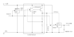
- Fig. 1 is the circuit principle diagram of the low dropout linear regulator circuit of related art
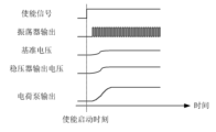
- FIG. 2 is a schematic diagram of voltage signal changes in a low dropout linear regulator circuit of the related art
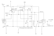
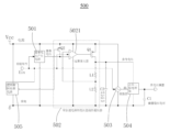
- Fig. 3 is the circuit schematic diagram of the low dropout linear voltage regulator circuit of embodiment one provided by the utility model
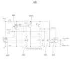
- Fig. 4 is the circuit schematic diagram of the low dropout linear voltage regulator circuit of embodiment two provided by the utility model
- Fig. 5 is the circuit schematic diagram of the low-dropout linear voltage regulator circuit of the third embodiment provided by the utility model
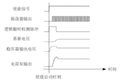
- FIG. 6 is a schematic diagram of voltage signal changes of the low dropout linear voltage regulator circuit provided by the embodiment of the present invention.
- FIG. 3 is a circuit diagram of a low-dropout linear voltage regulator circuit according to an embodiment of the present invention.
- the utility model provides a low-dropout linear voltage regulator circuit 100, comprising: an enable signal input terminal Ein, a reference voltage generating circuit 1, a low-dropout linear voltage regulator 2, an oscillator 3, and a forward double charge pump 4 , a high voltage bias output terminal Vout, a bias voltage stabilizing capacitor C1 and a logic inversion detection circuit 5 .
- the enable signal input terminal Ein is used for connecting an external enable signal.
- the reference voltage generation circuit 1 is used to generate a reference voltage, the input end of the reference voltage generation circuit 1 is connected to the enable signal input end Ein, the power supply end of the reference voltage generation circuit 1 is connected to the power supply voltage Vcc, the The ground terminal of the reference voltage generation circuit 1 is connected to the ground.
- the input of the low dropout linear regulator 2 is respectively connected to the power supply voltage Vcc, the output terminal of the reference voltage generating circuit 1, and the enable signal input terminal Ein.
- the input terminal of the oscillator 3 is connected to the enable signal input terminal Ein, the power supply terminal of the oscillator 3 is connected to the power supply voltage Vcc, and the ground terminal of the oscillator 3 is connected to ground.
- the first input end of the positive double charge pump 4 is connected to the output end of the oscillator 3, and the second input end of the positive double charge pump 4 is connected to the low dropout linear voltage regulator 2
- the output terminal of the positive double charge pump 4 is connected to the ground.
- the high voltage bias output terminal Fout is connected to the output terminal of the forward double charge pump 4 .
- the positive pole of the bias voltage stabilizing capacitor C1 is connected to the output terminal of the positive double charge pump 4, and the negative pole of the bias stabilizing capacitor C1 is connected to ground.
- the input terminal of the logic inversion detection circuit 5 is connected to the enable signal input terminal Ein, the power supply terminal of the logic inversion detection circuit 5 is connected to the power supply voltage Vcc, and the ground terminal of the logic inversion detection circuit 5 is connected to to ground, and the output end of the logic inversion detection circuit 5 is connected to the low dropout linear regulator 2 .
- the logic inversion detection circuit 5 is used to detect the inversion of the enable signal at the enable signal input terminal Ein, and output pulses to the low dropout linear regulator 2, so that the output of the low dropout linear regulator 2
- the output voltage at the terminal accelerates up to the power supply voltage.
- the positive double charge pump 4 will send charges to the bias voltage stabilizing capacitor C1 with higher efficiency than usual.
- After the pulse ends, after a short overshoot The output voltage can be stabilized at the required level, so that the establishment speed of the circuit can be improved, thereby effectively shortening the response time of the low-dropout linear voltage regulator circuit 100, and realizing a simple circuit with a small delay and a fast response Purpose.
- the low dropout linear regulator 2 includes a dual operational amplifier 21, a power transistor Q1, an acceleration pull-down transistor Q2, a first inductor L1 and a second inductor L2.
- the drain of the power transistor Q1 is sequentially connected to the ground after connecting the first inductor L1 and the second inductor L2 in series, and the drain of the power transistor Q1 is used as the output terminal of the low dropout linear regulator 2
- the source of the power transistor Q1 is connected to the power supply voltage Vcc, and the gate of the power transistor Q1 is connected to the output terminal of the dual operational amplifier 21 .
- the first operational amplifier non-inverting input terminal of the dual operational amplifier 21 is connected between the first inductor L1 and the second inductor L2, and the first operational amplifier inverting input terminal of the dual operational amplifier 21 is connected to The output terminal of the reference voltage generating circuit 1, the second operational amplifier non-inverting input terminal of the dual operational amplifier 21 is connected to the enable signal input terminal Ein, and the power supply terminal of the dual operational amplifier 21 is connected to the The power supply voltage Vcc, the ground terminal of the dual operational amplifier 21 is connected to the ground.
- the gate of the accelerated pull-down transistor Q2 is connected to the output terminal of the logic inversion detection circuit 5, the source of the accelerated pull-down transistor Q2 is connected to ground, and the drain of the accelerated pull-down transistor Q2 is connected to the power transistor Gate of Q1.
- the acceleration pull-down transistor Q2 is an NMOSFET, and the power transistor Q1 is a PMOSFET.
- the low dropout linear regulator circuit 100 further includes a reference voltage stabilizing capacitor C2, and the anode of the reference voltage stabilizing capacitor C2 is connected to the terminal of the low dropout linear regulator 2.
- the output terminal is connected to the drain of the power transistor Q1, and the second output terminal of the reference voltage stabilizing capacitor C2 is connected to ground.
- the enable signal of the enable signal input terminal Ein is reversed, the reference voltage generating circuit 1, the low dropout linear voltage regulator 2, and the oscillator 3 are all changed from the off state to the working state.
- the logic inversion detection circuit 5 detects the inversion of the enable signal, thereby outputting a pulse of a certain length as the signal for accelerating the circuit startup.
- the gate of the power transistor Q1 (PMOSFET) low, at this time the output voltage of the low dropout linear regulator 2 is quickly raised to the power supply voltage, and the positive double charge pump 4 will be higher than usual during the pulse.
- Efficiency delivers charge to the bias voltage stabilizing capacitor C1. After the pulse ends, the output voltage can be stabilized at the required level after a brief overshoot, which can increase the speed of circuit establishment.
- Figure 2 is a schematic diagram of the voltage signal change of the low-dropout linear regulator circuit of the related art
- Figure 6 is a voltage signal change of the low-dropout linear regulator circuit provided by the embodiment of the utility model schematic diagram.
- FIG. 4 it is a schematic circuit diagram of the low-dropout linear voltage regulator circuit of Embodiment 2 provided by the present invention.
- the low dropout linear voltage regulator circuit 400 of this embodiment is basically the same as the circuit structure of Embodiment 1, the difference is that the structure of the low dropout linear voltage regulator is different, specifically as follows:
- the low dropout linear regulator 402 includes a dual operational amplifier 4021, a power transistor Q1, an acceleration pull-down transistor Q2, a first inductor L1 and a second inductor L2.
- the drain of the power transistor Q1 is sequentially connected to the ground after connecting the first inductor L1 and the second inductor L2 in series, and the drain of the power transistor Q1 is used as the output terminal of the low dropout linear regulator 402 , the source of the power transistor Q1 is connected to the power supply voltage Vcc, and the gate of the power transistor Q1 is connected to the output terminal of the dual operational amplifier 4021 .
- the first operational amplifier non-inverting input terminal of the dual operational amplifier 4021 is connected between the first inductor L1 and the second inductor L2, and the first operational amplifier inverting input terminal of the dual operational amplifier 4021 is connected to The output terminal of the reference voltage generating circuit 401, the second operational amplifier non-inverting input terminal of the dual operational amplifier 4021 is connected to the enable signal input terminal Ein, and the power supply terminal of the dual operational amplifier 4021 is connected to the The power supply voltage Vcc, the ground terminal of the dual operational amplifier 4021 is connected to the ground.
- the gate of the accelerated pull-down transistor Q2 is connected to the output terminal of the logic inversion detection circuit 405, the source of the accelerated pull-down transistor Q2 is connected to ground, and the drain of the accelerated pull-down transistor Q2 is connected to the double operation The non-inverting input terminal of the first operational amplifier of the amplifier 4021.
- the acceleration pull-down transistor Q2 is an NMOSFET, and the power transistor Q1 is a PMOSFET.
- the enable signal of the enable signal input terminal Ein is reversed, the reference voltage generating circuit 401, the low dropout linear regulator 402, and the oscillator 403 are all changed from the off state to the working state, and these modules are started Before, the logic inversion detection circuit 405 outputs a pulse of a certain length as a signal for starting the acceleration circuit due to the detection of the inversion of the enable signal. Therefore, the operation of the operational amplifier 4021 is in the case of input saturation, and the output of the operational amplifier 4021 is pulled down to the lowest output voltage of the operational amplifier 4021.
- the power transistor Q1 (PMOSFET tube) will work in the linear region, and the low-dropout linear regulator
- the output voltage of 402 is quickly raised to the power supply voltage, and the positive double charge pump 404 will send charges to the bias voltage stabilizing capacitor C1 with higher efficiency than usual during the pulse, and after the pulse ends, after a short overshoot
- the output voltage is then stabilized at the desired level, which increases the speed of circuit settling.
- FIG. 5 it is a schematic circuit diagram of the low-dropout linear voltage regulator circuit of Embodiment 3 provided by the present invention.
- the low dropout linear voltage regulator circuit 500 of the embodiment is basically the same as the circuit structure of the first embodiment, the difference is that the structure of the low dropout linear voltage regulator is different, as follows:
- the low dropout linear regulator 502 includes a dual operational amplifier 5021, a power transistor Q1, an acceleration pull-up transistor Q2, a first inductor L1 and a second inductor L2.
- the drain of the power transistor Q1 is sequentially connected to the ground after connecting the first inductor L1 and the second inductor L2 in series, and the drain of the power transistor Q1 is used as the output terminal of the low dropout linear regulator 502 , the source of the power transistor Q1 is connected to the power supply voltage Vcc, and the gate of the power transistor Q1 is connected to the output terminal of the dual operational amplifier 5021 .
- the first operational amplifier non-inverting input terminal of the dual operational amplifier 5021 is connected between the first inductor L1 and the second inductor L2, and the first operational amplifier inverting input terminal of the dual operational amplifier 5021 is connected to The output end of the reference voltage generation circuit 501, the second operational amplifier non-inverting input end of the dual operational amplifier 5021 is connected to the enable signal input end Ein, and the power supply end of the dual operational amplifier 5021 is connected to the The power supply voltage Vcc, the ground terminal of the dual operational amplifier 5021 is connected to the ground.
- the gate of the accelerated pull-up transistor Q2 is connected to the output terminal of the logic inversion detection circuit 505, the source of the accelerated pull-up transistor Q2 is connected to the power supply voltage Vcc, and the drain of the accelerated pull-up transistor Q2 The pole is connected to the inverting input terminal of the first operational amplifier of the dual operational amplifier 4021.
- the acceleration pull-up transistor Q2 is a PMOSFET
- the power transistor Q1 is a PMOSFET
- the enable signal of the enable signal input terminal Ein is reversed, the reference voltage generating circuit 501, the low dropout linear regulator 502, and the oscillator 503 are all changed from the off state to the working state, and these modules are started Before, the logic inversion detection circuit 505 outputs a pulse of a certain length as a signal for starting the acceleration circuit due to detection of the inversion of the enable signal.
- the signal causes the acceleration pull-up transistor Q2 ( PMOSFET tube) is turned on, so that the reference voltage of the input of the operational amplifier 5021 is raised to the power supply voltage, so that the operation of the operational amplifier 5021 is in the case of input saturation, and the output of the operational amplifier 5021 is then pulled down to the lowest value of the operational amplifier 5021 Therefore, the power transistor Q1 (PMOSFET tube) will work in the linear region, the output voltage of the low-dropout linear regulator 502 will be quickly raised to the power supply voltage, and the forward double charge pump 504 will be higher than usual during the pulse.
- the high efficiency sends charge to the bias voltage stabilizing capacitor C1. After the end of the pulse, the output voltage can be stabilized at the required level after a short overshoot, which can increase the speed of circuit establishment.
- the embodiment of the utility model also provides a radio frequency switch, which includes the above-mentioned low-dropout linear voltage regulator circuit provided by the embodiment of the utility model.
- the technical effect achieved by the radio-frequency switch is the same as the above-mentioned low-dropout linear voltage regulator circuit. This will not be repeated here.
- the low-dropout linear voltage regulator includes dual operational amplifiers and power transistors, and an acceleration-establishing transistor is added to accelerate the establishment of the transistor. pull-up transistors or speed up pull-down transistors.
- the logic inversion detection circuit detects the enable signal Inversion, so as to output a pulse of a certain length as the signal to start the acceleration circuit, so that the output voltage of the low-dropout linear regulator is quickly raised to the power supply voltage, and the forward double charge pump will use higher efficiency than usual during the pulse.
- the bias voltage stabilizing capacitor sends the charge. After the pulse ends, the output voltage can be stabilized at the required level after a short overshoot.
- the response time of the voltage regulator circuit and the radio frequency switch is realized, and the simple circuit achieves the purpose of small delay and fast response.
Landscapes
- Engineering & Computer Science (AREA)
- Physics & Mathematics (AREA)
- Electromagnetism (AREA)
- General Physics & Mathematics (AREA)
- Radar, Positioning & Navigation (AREA)
- Automation & Control Theory (AREA)
- Continuous-Control Power Sources That Use Transistors (AREA)
Abstract
一种低压差线性稳压器电路(100,400,500),包括使能信号输入端(Ein)、基准电压产生电路(1,401,501)、低压差线性稳压器(2,402,502)、振荡器(3,403,503)、正向二倍电荷泵(4,404,504)、高电压偏置输出端(Vout)、偏置稳压电容(C1)、逻辑翻转检测电路(5,405,505);逻辑翻转检测电路(5,405,505)用于检测使能信号输入端(Ein)的使能信号翻转后,输出脉冲至低压差线性稳压器(2,402,502),使低压差线性稳压器(2,402,502)的输出端的输出电压加速抬升至电源电压(Vcc)。低压差线性稳压器电路(100,400,500)及射频开关延迟小、响应速度快。
Description
本实用新型涉及无线通信射频开关技术领域,尤其涉及一种射频开关正向偏置电压加速建立的低压差线性稳压器电路及射频开关。
射频开关广泛应用于无线通信设备中,使用在需要对射频信号进行导通或截止的场合,例如发射接收开关、通道选择开关、调谐开关、换向开关等。目前综合成本和性能的考量,无线通信设备中通常使用硅衬底-掩埋氧化层—外沿硅(SOI)技术,在外沿硅上生长金属氧化物场效应晶体管(MOS)器件来制作射频开关电路。现今的手持设备中为提高集成度,通常省略射频开关的常压模拟电源,仅保留串行控制接口的低压数字电源,因此射频开关需要使用低压电源为常压工作的射频器件提供偏置。
现有技术中如图1所示,射频开关转换电源电压通常使用低压差线性稳压器将电压稳定在常压的一半,然后用正向二倍电荷泵将其提升至射频器件所需的电压。同时为了低功耗的需求,在不需要该射频开关链路工作时串行控制接口将关闭所有的控制电路仅保留接口的供电。但是每当需要启动时如图2所示,由于基准电压产生电路和低压差线性稳压器本身的响应慢,加上振荡器和二倍电荷泵的响应延迟,使得射频开关自收到串行控制的使能信号后有较长的时间内无法提供正确的功能,响应速度慢。
因此,有必要提供一种新的低压差线性稳压器电路及射频开关以解决上述技术问题。
实用新型内容
针对以上相关技术的不足,本实用新型提出一种延迟小、响应速度快的低压差线性稳压器电路及射频开关。
为了解决上述技术问题,本实用新型实施例提供了一种低压差线性稳压器电路,包括:
使能信号输入端,用于连接外部使能信号;
基准电压产生电路,用于产生基准电压,所述基准电压产生电路的输入端与所述使能信号输入端连接,所述基准电压产生电路的电源端与电源电压连接,所述基准电压产生电路的接地端连接至接地;
低压差线性稳压器,所述低压差线性稳压器的输入分别连接至所述电源电压、所述基准电压产生电路的输出端、所述使能信号输入端;
振荡器,所述振荡器的输入端连接至所述使能信号输入端,所述振荡器的电源端连接至电源电压,所述振荡器的接地端连接至接地;
正向二倍电荷泵,所述正向二倍电荷泵的第一输入端连接至所述振荡器的输出端,所述正向二倍电荷泵的第二输入端连接至所述低压差线性稳压器的输出端,所述正向二倍电荷泵的接地端连接至接地;
高电压偏置输出端,所述高电压偏置输出端连接至所述正向二倍电荷泵的输出端;
偏置稳压电容,所述偏置稳压电容的正极连接至所述正向二倍电荷泵的输出端,所述偏置稳压电容的负极连接至接地;
逻辑翻转检测电路,所述逻辑翻转检测电路的输入端连接至所述使能信号输入端,所述逻辑翻转检测电路的电源端连接至所述电源电压,所述逻辑翻转检测电路的接地端连接至接地,所述逻辑翻转检测电路的输出端连接至所述低压差线性稳压器;所述逻辑翻转检测电路用于检测所述使能信号输入端的使能信号翻转后,输出脉冲至所述低压差线性稳压器,使所述低压差线性稳压器的输出端的输出电压加速抬升至所述电源电压。
优选的,所述低压差线性稳压器包括双运算放大器、功率晶体管、 加速下拉晶体管、第一电感和第二电感;所述功率晶体管的漏极依次串联所述第一电感和所述第二电感后连接至接地,且所述功率晶体管的漏极作为所述低压差线性稳压器的输出端,所述功率晶体管的源极连接至所述电源电压,所述功率晶体管的栅极连接至所述双运算放大器的输出端;所述双运算放大器的第一运放同向输入端连接至所述第一电感与所述第二电感之间,所述双运算放大器的第一运放反向输入端连接至所述基准电压产生电路的输出端,所述双运算放大器的第二运放同向输入端连接至所述使能信号输入端,所述双运算放大器的电源端连接至所述电源电压,所述双运算放大器的接地端连接至接地;所述加速下拉晶体管的栅极连接至所述逻辑翻转检测电路的输出端,所述加速下拉晶体管的源极连接至接地,所述加速下拉晶体管的漏极连接至所述功率晶体管的栅极。
优选的,所述低压差线性稳压器包括双运算放大器、功率晶体管、加速下拉晶体管、第一电感和第二电感;所述功率晶体管的漏极依次串联所述第一电感和所述第二电感后连接至接地,且所述功率晶体管的漏极作为所述低压差线性稳压器的输出端,所述功率晶体管的源极连接至所述电源电压,所述功率晶体管的栅极连接至所述双运算放大器的输出端;所述双运算放大器的第一运放同向输入端连接至所述第一电感与所述第二电感之间,所述双运算放大器的第一运放反向输入端连接至所述基准电压产生电路的输出端,所述双运算放大器的第二运放同向输入端连接至所述使能信号输入端,所述双运算放大器的电源端连接至所述电源电压,所述双运算放大器的接地端连接至接地;所述加速下拉晶体管的栅极连接至所述逻辑翻转检测电路的输出端,所述加速下拉晶体管的源极连接至接地,所述加速下拉晶体管的漏极连接至所述双运算放大器的第一运放同向输入端。
优选的,所述加速下拉晶体管为NMOSFET管,所述功率晶体管为PMOSFET管。
优选的,所述低压差线性稳压器包括双运算放大器、功率晶体管、 加速上拉晶体管、第一电感和第二电感;所述功率晶体管的漏极依次串联所述第一电感和所述第二电感后连接至接地,且所述功率晶体管的漏极作为所述低压差线性稳压器的输出端,所述功率晶体管的源极连接至所述电源电压,所述功率晶体管的栅极连接至所述双运算放大器的输出端;所述双运算放大器的第一运放同向输入端连接至所述第一电感与所述第二电感之间,所述双运算放大器的第一运放反向输入端连接至所述基准电压产生电路的输出端,所述双运算放大器的第二运放同向输入端连接至所述使能信号输入端,所述双运算放大器的电源端连接至所述电源电压,所述双运算放大器的接地端连接至接地;所述加速上拉晶体管的栅极连接至所述逻辑翻转检测电路的输出端,所述加速上拉晶体管的源极连接至所述电源电压,所述加速上拉晶体管的漏极连接至所述双运算放大器的第一运放反向输入端。
优选的,所述加速上拉晶体管为PMOSFET管,所述功率晶体管为PMOSFET管。
优选的,还包括参考电压稳压电容,所述参考电压稳压电容的正极连接至所述低压差线性稳压器的输出端,所述参考电压稳压电容的第二输出端连接至接地。
本实用新型实施例还提供一种射频开关,其包括本实用新型实施例提供的上述低压差线性稳压器电路。
与相关技术相比,本实用新型的低压差线性稳压器电路及射频开关中,低压差线性稳压器包括双运算放大器和功率晶体管,并增加设置了加速建立晶体管,加速建立晶体管为加速上拉晶体管或加速下拉晶体管。通过将加速建立晶体管的栅极连接至所述逻辑翻转检测电路的输出端,同时将其漏极连接至双运算放大器的输入或功率晶体管的输入,从而,逻辑翻转检测电路由于检测到使能信号翻转,从而输出一定长度的脉冲作为加速电路启动的信号,使得低压差线性稳压器的输出电压被快速抬升至电源电压,正向二倍电荷泵在脉冲期间将以比平时更高的效率为偏置稳压电容送电荷,在脉冲结束后,经历短暂的 过冲后输出电压即可稳定在所需的电平上,如此即可提升电路的建立速度,从而有效的缩短了低压差线性稳压器电路及射频开关的响应时间,实现了简单电路达到延迟小,响应快的目的。
下面结合附图详细说明本实用新型。通过结合以下附图所作的详细描述,本实用新型的上述或其他方面的内容将变得更清楚和更容易理解。附图中:
图1为相关技术的低压差线性稳压器电路的电路原理图;
图2为相关技术的低压差线性稳压器电路的电压信号变化示意图;
图3为本实用新型提供的实施例一的低压差线性稳压器电路的电路原理图;
图4为本实用新型提供的实施例二的低压差线性稳压器电路的电路原理图;
图5为本实用新型提供的实施例三的低压差线性稳压器电路的电路原理图;
图6为本实用新型实施例提供的低压差线性稳压器电路的电压信号变化示意图。
下面结合附图详细说明本实用新型的具体实施方式。
在此记载的具体实施方式/实施例为本实用新型的特定的具体实施方式,用于说明本实用新型的构思,均是解释性和示例性的,不应解释为对本实用新型实施方式及本实用新型范围的限制。除在此记载的实施例外,本领域技术人员还能够基于本申请权利要求书和说明书所公开的内容采用显而易见的其它技术方案,这些技术方案包括采用对在此记载的实施例的做出任何显而易见的替换和修改的技术方案, 都在本实用新型的保护范围之内。
以下各实施例的说明是参考附加的图式,用以例示本实用新型可用以实施的特定实施例。本实用新型所提到的方向用语,例如上、下、前、后、左、右、内、外、侧面等,仅是参考附加图式的方向。因此,使用的方向用语是用以说明及理解本实用新型,而非用以限制本实用新型。
实施例一
请参图3所示,为本实用新型提供的实施例一低压差线性稳压器电路的电路图。本实用新型提供了一种低压差线性稳压器电路100,包括:使能信号输入端Ein、基准电压产生电路1、低压差线性稳压器2、振荡器3、正向二倍电荷泵4、高电压偏置输出端Vout、偏置稳压电容C1以及逻辑翻转检测电路5。
使能信号输入端Ein,用于连接外部使能信号。
基准电压产生电路1用于产生基准电压,所述基准电压产生电路1的输入端与所述使能信号输入端Ein连接,所述基准电压产生电路1的电源端与电源电压Vcc连接,所述基准电压产生电路1的接地端连接至接地。
所述低压差线性稳压器2的输入分别连接至所述电源电压Vcc、所述基准电压产生电路1的输出端、所述使能信号输入端Ein。
所述振荡器3的输入端连接至所述使能信号输入端Ein,所述振荡器3的电源端连接至电源电压Vcc,所述振荡器3的接地端连接至接地。
所述正向二倍电荷泵4的第一输入端连接至所述振荡器3的输出端,所述正向二倍电荷泵4的第二输入端连接至所述低压差线性稳压器2的输出端,所述正向二倍电荷泵4的接地端连接至接地。
所述高电压偏置输出端Fout连接至所述正向二倍电荷泵4的输出端。
所述偏置稳压电容C1的正极连接至所述正向二倍电荷泵4的输出 端,所述偏置稳压电容C1的负极连接至接地。
所述逻辑翻转检测电路5的输入端连接至所述使能信号输入端Ein,所述逻辑翻转检测电路5的电源端连接至所述电源电压Vcc,所述逻辑翻转检测电路5的接地端连接至接地,所述逻辑翻转检测电路5的输出端连接至所述低压差线性稳压器2。
所述逻辑翻转检测电路5用于检测所述使能信号输入端Ein的使能信号翻转后,输出脉冲至所述低压差线性稳压器2,使所述低压差线性稳压器2的输出端的输出电压加速抬升至所述电源电压,正向二倍电荷泵4在脉冲期间将以比平时更高的效率为偏置稳压电容C1送电荷,在脉冲结束后,经历短暂的过冲后输出电压即可稳定在所需的电平上,如此即可提升电路的建立速度,从而有效的缩短了低压差线性稳压器电路100的响应时间,实现了简单电路达到延迟小,响应快的目的。
本实施方式中,具体的,所述低压差线性稳压器2包括双运算放大器21、功率晶体管Q1、加速下拉晶体管Q2、第一电感L1和第二电感L2。
所述功率晶体管Q1的漏极依次串联所述第一电感L1和所述第二电感L2后连接至接地,且所述功率晶体管Q1的漏极作为所述低压差线性稳压器2的输出端;所述功率晶体管Q1的源极连接至所述电源电压Vcc,所述功率晶体管Q1的栅极连接至所述双运算放大器21的输出端。
所述双运算放大器21的第一运放同向输入端连接至所述第一电感L1与所述第二电感L2之间,所述双运算放大器21的第一运放反向输入端连接至所述基准电压产生电路1的输出端,所述双运算放大器21的第二运放同向输入端连接至所述使能信号输入端Ein,所述双运算放大器21的电源端连接至所述电源电压Vcc,所述双运算放大器21的接地端连接至接地。
所述加速下拉晶体管Q2的栅极连接至所述逻辑翻转检测电路5 的输出端,所述加速下拉晶体管Q2的源极连接至接地,所述加速下拉晶体管Q2的漏极连接至所述功率晶体管Q1的栅极。
其中,所述加速下拉晶体管Q2为NMOSFET管,所述功率晶体管Q1为PMOSFET管。
更优的,本实施方式中,所述低压差线性稳压器电路100还包括参考电压稳压电容C2,所述参考电压稳压电容C2的正极连接至所述低压差线性稳压器2的输出端,即连接至所述功率晶体管Q1的漏极,所述参考电压稳压电容C2的第二输出端连接至接地。
本实施方式中,使能信号输入端Ein的使能信号翻转,基准电压产生电路1,低压差线性稳压器2,振荡器3均由关断状态变为工作状态,在这些模块完成启动之前,逻辑翻转检测电路5由于检测到使能信号翻转,从而输出一定长度的脉冲作为加速电路启动的信号,本实施方式中,该信号使加速建立的加速下拉晶体管Q2(NMOSFET管)导通,从而使功率晶体管Q1(PMOSFET管)的栅极置低,此时低压差线性稳压器2的输出电压被快速抬升至电源电压,正向二倍电荷泵4在脉冲期间将以比平时更高的效率为偏置稳压电容C1送电荷,在脉冲结束后,经历短暂的过冲后输出电压即可稳定在所需的电平上,如此即可提升电路的建立速度。
请结合图2和图6所示,图2为相关技术的低压差线性稳压器电路的电压信号变化示意图;图6为本实用新型实施例提供的低压差线性稳压器电路的电压信号变化示意图。由图2和图6比较可知,本实用新型的低压差线性稳压器电路的正向二倍电荷泵4的稳定输出时间明显缩短,即有效的缩短了低压差线性稳压器电路及射频开关的响应时间,实现了简单电路达到延迟小,响应快的目的。
实施例二
如图4所示,为本实用新型提供的实施例二的低压差线性稳压器电路的电路原理图。本实施方式的低压差线性稳压器电路400与实施 方式一的电路结构基本相同,不同在于低压差线性稳压器的结构不同,具体如下:
本实施方式中,所述低压差线性稳压器402包括双运算放大器4021、功率晶体管Q1、加速下拉晶体管Q2、第一电感L1和第二电感L2。
所述功率晶体管Q1的漏极依次串联所述第一电感L1和所述第二电感L2后连接至接地,且所述功率晶体管Q1的漏极作为所述低压差线性稳压器402的输出端,所述功率晶体管Q1的源极连接至所述电源电压Vcc,所述功率晶体管Q1的栅极连接至所述双运算放大器4021的输出端。
所述双运算放大器4021的第一运放同向输入端连接至所述第一电感L1与所述第二电感L2之间,所述双运算放大器4021的第一运放反向输入端连接至所述基准电压产生电路401的输出端,所述双运算放大器4021的第二运放同向输入端连接至所述使能信号输入端Ein,所述双运算放大器4021的电源端连接至所述电源电压Vcc,所述双运算放大器4021的接地端连接至接地。
所述加速下拉晶体管Q2的栅极连接至所述逻辑翻转检测电路405的输出端,所述加速下拉晶体管Q2的源极连接至接地,所述加速下拉晶体管Q2的漏极连接至所述双运算放大器4021的第一运放同向输入端。
其中,所述加速下拉晶体管Q2为NMOSFET管,所述功率晶体管Q1为PMOSFET管。
本实施方式中,使能信号输入端Ein的使能信号翻转,基准电压产生电路401,低压差线性稳压器402,振荡器403,均由关断状态变为工作状态,在这些模块完成启动之前,逻辑翻转检测电路405由于检测到使能信号翻转,从而输出一定长度的脉冲作为加速电路启动的信号,本实施例中,该信号使加速建立的加速下拉晶体管Q2(NMOSFET管)导通,从而使运算放大器4021的工作在输入饱和的 情况,运算放大器4021的输出随即被下拉至运算放大器4021的最低输出电压,因此功率晶体管Q1(PMOSFET管)会工作在线性区,低压差线性稳压器402的输出电压被快速抬升至电源电压,正向二倍电荷泵404在脉冲期间将以比平时更高的效率为偏置稳压电容C1送电荷,在脉冲结束后,经历短暂的过冲后输出电压即可稳定在所需的电平上,如此即可提升电路的建立速度。
除上述区别外,其他结构及原理与实施一相同,在此不再赘述。
实施例三
如图5所示,为本实用新型提供的实施例三的低压差线性稳压器电路的电路原理图。实施方式的低压差线性稳压器电路500与实施方式一的电路结构基本相同,不同在于低压差线性稳压器的结构不同,具体如下:
本实施方式中,所述低压差线性稳压器502包括双运算放大器5021、功率晶体管Q1、加速上拉晶体管Q2、第一电感L1和第二电感L2。
所述功率晶体管Q1的漏极依次串联所述第一电感L1和所述第二电感L2后连接至接地,且所述功率晶体管Q1的漏极作为所述低压差线性稳压器502的输出端,所述功率晶体管Q1的源极连接至所述电源电压Vcc,所述功率晶体管Q1的栅极连接至所述双运算放大器5021的输出端。
所述双运算放大器5021的第一运放同向输入端连接至所述第一电感L1与所述第二电感L2之间,所述双运算放大器5021的第一运放反向输入端连接至所述基准电压产生电路501的输出端,所述双运算放大器5021的第二运放同向输入端连接至所述使能信号输入端Ein,所述双运算放大器5021的电源端连接至所述电源电压Vcc,所述双运算放大器5021的接地端连接至接地。
所述加速上拉晶体管Q2的栅极连接至所述逻辑翻转检测电路505 的输出端,所述加速上拉晶体管Q2的源极连接至所述电源电压Vcc,所述加速上拉晶体管Q2的漏极连接至所述双运算放大器4021的第一运放反向输入端。
其中,所述加速上拉晶体管Q2为PMOSFET管,所述功率晶体管Q1为PMOSFET管。
本实施方式中,使能信号输入端Ein的使能信号翻转,基准电压产生电路501,低压差线性稳压器502,振荡器503,均由关断状态变为工作状态,在这些模块完成启动之前,逻辑翻转检测电路505由于检测到使能信号翻转,从而输出一定长度的脉冲作为加速电路启动的信号,本实施例中,该信号在经历反相后使加速建立的加速上拉晶体管Q2(PMOSFET管)导通,如此将使运算放大器5021的输入的基准电压被抬升至电源电压,从而使运算放大器5021的工作在输入饱和的情况,运算放大器5021的输出随即被下拉至运算放大器5021的最低输出电压,因此功率晶体管Q1(PMOSFET管)会工作在线性区,低压差线性稳压器502的输出电压被快速抬升至电源电压,正向二倍电荷泵504在脉冲期间将以比平时更高的效率为偏置稳压电容C1送电荷,在脉冲结束后,经历短暂的过冲后输出电压即可稳定在所需的电平上,如此即可提升电路的建立速度。
除上述区别外,其他结构及原理与实施一相同,在此不再赘述。
本实用新型实施例还提供一种射频开关,其包括本实用新型实施例提供的上述低压差线性稳压器电路,所述射频开关实现的技术效果与上述低压差线性稳压器电路相同,在此不再赘述。
与相关技术相比,本实用新型的低压差线性稳压器电路及射频开关中,低压差线性稳压器包括双运算放大器和功率晶体管,并增加设置了加速建立晶体管,加速建立晶体管为加速上拉晶体管或加速下拉晶体管。通过将加速建立晶体管的栅极连接至所述逻辑翻转检测电路的输出端,同时将其漏极连接至双运算放大器的输入或功率晶体管的输入,从而,逻辑翻转检测电路由于检测到使能信号翻转,从而输出 一定长度的脉冲作为加速电路启动的信号,使得低压差线性稳压器的输出电压被快速抬升至电源电压,正向二倍电荷泵在脉冲期间将以比平时更高的效率为偏置稳压电容送电荷,在脉冲结束后,经历短暂的过冲后输出电压即可稳定在所需的电平上,如此即可提升电路的建立速度,从而有效的缩短了低压差线性稳压器电路及射频开关的响应时间,实现了简单电路达到延迟小,响应快的目的。
需要说明的是,以上参照附图所描述的各个实施例仅用以说明本实用新型而非限制本实用新型的范围,本领域的普通技术人员应当理解,在不脱离本实用新型的精神和范围的前提下对本实用新型进行的修改或者等同替换,均应涵盖在本实用新型的范围之内。此外,除上下文另有所指外,以单数形式出现的词包括复数形式,反之亦然。另外,除非特别说明,那么任何实施例的全部或一部分可结合任何其它实施例的全部或一部分来使用。
Claims (8)
- 一种低压差线性稳压器电路,其特征在于,包括,使能信号输入端,用于连接外部使能信号;基准电压产生电路,用于产生基准电压,所述基准电压产生电路的输入端与所述使能信号输入端连接,所述基准电压产生电路的电源端与电源电压连接,所述基准电压产生电路的接地端连接至接地;低压差线性稳压器,所述低压差线性稳压器的输入分别连接至所述电源电压、所述基准电压产生电路的输出端、所述使能信号输入端;振荡器,所述振荡器的输入端连接至所述使能信号输入端,所述振荡器的电源端连接至电源电压,所述振荡器的接地端连接至接地;正向二倍电荷泵,所述正向二倍电荷泵的第一输入端连接至所述振荡器的输出端,所述正向二倍电荷泵的第二输入端连接至所述低压差线性稳压器的输出端,所述正向二倍电荷泵的接地端连接至接地;高电压偏置输出端,所述高电压偏置输出端连接至所述正向二倍电荷泵的输出端;偏置稳压电容,所述偏置稳压电容的正极连接至所述正向二倍电荷泵的输出端,所述偏置稳压电容的负极连接至接地;逻辑翻转检测电路,所述逻辑翻转检测电路的输入端连接至所述使能信号输入端,所述逻辑翻转检测电路的电源端连接至所述电源电压,所述逻辑翻转检测电路的接地端连接至接地,所述逻辑翻转检测电路的输出端连接至所述低压差线性稳压器;所述逻辑翻转检测电路用于检测所述使能信号输入端的使能信号翻转后,输出脉冲至所述低压差线性稳压器,使所述低压差线性稳压器的输出端的输出电压加速抬升至所述电源电压。
- 根据权利要求1所述的低压差线性稳压器电路,其特征在于,所述低压差线性稳压器包括双运算放大器、功率晶体管、加速下拉晶体管、第一电感和第二电感;所述功率晶体管的漏极依次串联所述第 一电感和所述第二电感后连接至接地,且所述功率晶体管的漏极作为所述低压差线性稳压器的输出端,所述功率晶体管的源极连接至所述电源电压,所述功率晶体管的栅极连接至所述双运算放大器的输出端;所述双运算放大器的第一运放同向输入端连接至所述第一电感与所述第二电感之间,所述双运算放大器的第一运放反向输入端连接至所述基准电压产生电路的输出端,所述双运算放大器的第二运放同向输入端连接至所述使能信号输入端,所述双运算放大器的电源端连接至所述电源电压,所述双运算放大器的接地端连接至接地;所述加速下拉晶体管的栅极连接至所述逻辑翻转检测电路的输出端,所述加速下拉晶体管的源极连接至接地,所述加速下拉晶体管的漏极连接至所述功率晶体管的栅极。
- 根据权利要求1所述的低压差线性稳压器电路,其特征在于,所述低压差线性稳压器包括双运算放大器、功率晶体管、加速下拉晶体管、第一电感和第二电感;所述功率晶体管的漏极依次串联所述第一电感和所述第二电感后连接至接地,且所述功率晶体管的漏极作为所述低压差线性稳压器的输出端,所述功率晶体管的源极连接至所述电源电压,所述功率晶体管的栅极连接至所述双运算放大器的输出端;所述双运算放大器的第一运放同向输入端连接至所述第一电感与所述第二电感之间,所述双运算放大器的第一运放反向输入端连接至所述基准电压产生电路的输出端,所述双运算放大器的第二运放同向输入端连接至所述使能信号输入端,所述双运算放大器的电源端连接至所述电源电压,所述双运算放大器的接地端连接至接地;所述加速下拉晶体管的栅极连接至所述逻辑翻转检测电路的输出端,所述加速下拉晶体管的源极连接至接地,所述加速下拉晶体管的漏极连接至所述双运算放大器的第一运放同向输入端。
- 根据权利要求2或3所述的低压差线性稳压器电路,其特征在于,所述加速下拉晶体管为NMOSFET管,所述功率晶体管为PMOSFET管。
- 根据权利要求1所述的低压差线性稳压器电路,其特征在于,所述低压差线性稳压器包括双运算放大器、功率晶体管、加速上拉晶体管、第一电感和第二电感;所述功率晶体管的漏极依次串联所述第一电感和所述第二电感后连接至接地,且所述功率晶体管的漏极作为所述低压差线性稳压器的输出端,所述功率晶体管的源极连接至所述电源电压,所述功率晶体管的栅极连接至所述双运算放大器的输出端;所述双运算放大器的第一运放同向输入端连接至所述第一电感与所述第二电感之间,所述双运算放大器的第一运放反向输入端连接至所述基准电压产生电路的输出端,所述双运算放大器的第二运放同向输入端连接至所述使能信号输入端,所述双运算放大器的电源端连接至所述电源电压,所述双运算放大器的接地端连接至接地;所述加速上拉晶体管的栅极连接至所述逻辑翻转检测电路的输出端,所述加速上拉晶体管的源极连接至所述电源电压,所述加速上拉晶体管的漏极连接至所述双运算放大器的第一运放反向输入端。
- 根据权利要求5所述的低压差线性稳压器电路,其特征在于,所述加速上拉晶体管为PMOSFET管,所述功率晶体管为PMOSFET管。
- 根据权利要求1所述的低压差线性稳压器电路,其特征在于,还包括参考电压稳压电容,所述参考电压稳压电容的正极连接至所述低压差线性稳压器的输出端,所述参考电压稳压电容的第二输出端连接至接地。
- 一种射频开关,其特征在于,包括如权利要求1-7任意一项所述的低压差线性稳压器电路。
Applications Claiming Priority (2)
| Application Number | Priority Date | Filing Date | Title |
|---|---|---|---|
| CN202122690996.1 | 2021-11-03 | ||
| CN202122690996.1U CN216387888U (zh) | 2021-11-03 | 2021-11-03 | 低压差线性稳压器电路及射频开关 |
Publications (1)
| Publication Number | Publication Date |
|---|---|
| WO2023078063A1 true WO2023078063A1 (zh) | 2023-05-11 |
Family
ID=81249285
Family Applications (1)
| Application Number | Title | Priority Date | Filing Date |
|---|---|---|---|
| PCT/CN2022/125444 Ceased WO2023078063A1 (zh) | 2021-11-03 | 2022-10-14 | 低压差线性稳压器电路及射频开关 |
Country Status (2)
| Country | Link |
|---|---|
| CN (1) | CN216387888U (zh) |
| WO (1) | WO2023078063A1 (zh) |
Cited By (5)
| Publication number | Priority date | Publication date | Assignee | Title |
|---|---|---|---|---|
| CN116736924A (zh) * | 2023-08-11 | 2023-09-12 | 荣湃半导体(上海)有限公司 | 一种宽输入范围低功耗的稳压源电路和电子设备 |
| CN117278015A (zh) * | 2023-11-21 | 2023-12-22 | 成都怡康科技有限公司 | 一种低功耗多触发源开关机电路 |
| CN117724567A (zh) * | 2023-12-25 | 2024-03-19 | 圣邦微电子(北京)股份有限公司 | 带隙基准电路及低压差线性稳压器 |
| CN119341536A (zh) * | 2024-12-18 | 2025-01-21 | 无锡中微爱芯电子有限公司 | 一种驱动管衬底切换改善ldo过冲的电路 |
| CN119597095A (zh) * | 2025-02-11 | 2025-03-11 | 芯洲科技(北京)股份有限公司 | 线性稳压电路和电源芯片 |
Families Citing this family (3)
| Publication number | Priority date | Publication date | Assignee | Title |
|---|---|---|---|---|
| CN216387888U (zh) * | 2021-11-03 | 2022-04-26 | 深圳飞骧科技股份有限公司 | 低压差线性稳压器电路及射频开关 |
| US12184174B2 (en) * | 2022-10-05 | 2024-12-31 | Murata Manufacturing Co., Ltd. | Reduced gate drive for power converter with dynamically switching ratio |
| CN116191850B (zh) * | 2023-04-28 | 2023-06-27 | 上海灵动微电子股份有限公司 | 基准电压的防过冲电路 |
Citations (9)
| Publication number | Priority date | Publication date | Assignee | Title |
|---|---|---|---|---|
| US20110285456A1 (en) * | 2009-02-06 | 2011-11-24 | Arizona Board Of Regents For And On Behalf Of Arizona State University | Four-terminal soi mesfet based low dropout regulator |
| CN104796171A (zh) * | 2015-03-25 | 2015-07-22 | 广州钧衡微电子科技有限公司 | 一种应用于soi cmos射频开关的控制电路 |
| CN105786074A (zh) * | 2016-04-20 | 2016-07-20 | 广东工业大学 | 一种soi cmos射频开关电路结构 |
| US20170163218A1 (en) * | 2015-12-08 | 2017-06-08 | Skyworks Solutions, Inc. | Low dropout voltage regulator for highly linear radio frequency power amplifiers |
| CN107039081A (zh) * | 2016-01-11 | 2017-08-11 | 桑迪士克科技有限责任公司 | 快速设置低压降调节器 |
| CN112256081A (zh) * | 2020-10-27 | 2021-01-22 | 电子科技大学 | 一种带自适应电荷泵的低压差线性稳压器 |
| CN113050507A (zh) * | 2021-03-26 | 2021-06-29 | 广州穗源微电子科技有限公司 | 一种应用于低电源电压射频开关的控制电路 |
| CN216387888U (zh) * | 2021-11-03 | 2022-04-26 | 深圳飞骧科技股份有限公司 | 低压差线性稳压器电路及射频开关 |
| CN216390950U (zh) * | 2021-11-03 | 2022-04-26 | 深圳飞骧科技股份有限公司 | 射频开关正向偏置加速建立电路及射频开关 |
-
2021
- 2021-11-03 CN CN202122690996.1U patent/CN216387888U/zh active Active
-
2022
- 2022-10-14 WO PCT/CN2022/125444 patent/WO2023078063A1/zh not_active Ceased
Patent Citations (9)
| Publication number | Priority date | Publication date | Assignee | Title |
|---|---|---|---|---|
| US20110285456A1 (en) * | 2009-02-06 | 2011-11-24 | Arizona Board Of Regents For And On Behalf Of Arizona State University | Four-terminal soi mesfet based low dropout regulator |
| CN104796171A (zh) * | 2015-03-25 | 2015-07-22 | 广州钧衡微电子科技有限公司 | 一种应用于soi cmos射频开关的控制电路 |
| US20170163218A1 (en) * | 2015-12-08 | 2017-06-08 | Skyworks Solutions, Inc. | Low dropout voltage regulator for highly linear radio frequency power amplifiers |
| CN107039081A (zh) * | 2016-01-11 | 2017-08-11 | 桑迪士克科技有限责任公司 | 快速设置低压降调节器 |
| CN105786074A (zh) * | 2016-04-20 | 2016-07-20 | 广东工业大学 | 一种soi cmos射频开关电路结构 |
| CN112256081A (zh) * | 2020-10-27 | 2021-01-22 | 电子科技大学 | 一种带自适应电荷泵的低压差线性稳压器 |
| CN113050507A (zh) * | 2021-03-26 | 2021-06-29 | 广州穗源微电子科技有限公司 | 一种应用于低电源电压射频开关的控制电路 |
| CN216387888U (zh) * | 2021-11-03 | 2022-04-26 | 深圳飞骧科技股份有限公司 | 低压差线性稳压器电路及射频开关 |
| CN216390950U (zh) * | 2021-11-03 | 2022-04-26 | 深圳飞骧科技股份有限公司 | 射频开关正向偏置加速建立电路及射频开关 |
Cited By (7)
| Publication number | Priority date | Publication date | Assignee | Title |
|---|---|---|---|---|
| CN116736924A (zh) * | 2023-08-11 | 2023-09-12 | 荣湃半导体(上海)有限公司 | 一种宽输入范围低功耗的稳压源电路和电子设备 |
| CN116736924B (zh) * | 2023-08-11 | 2023-11-03 | 荣湃半导体(上海)有限公司 | 一种宽输入范围低功耗的稳压源电路和电子设备 |
| CN117278015A (zh) * | 2023-11-21 | 2023-12-22 | 成都怡康科技有限公司 | 一种低功耗多触发源开关机电路 |
| CN117278015B (zh) * | 2023-11-21 | 2024-01-30 | 成都怡康科技有限公司 | 一种低功耗多触发源开关机电路 |
| CN117724567A (zh) * | 2023-12-25 | 2024-03-19 | 圣邦微电子(北京)股份有限公司 | 带隙基准电路及低压差线性稳压器 |
| CN119341536A (zh) * | 2024-12-18 | 2025-01-21 | 无锡中微爱芯电子有限公司 | 一种驱动管衬底切换改善ldo过冲的电路 |
| CN119597095A (zh) * | 2025-02-11 | 2025-03-11 | 芯洲科技(北京)股份有限公司 | 线性稳压电路和电源芯片 |
Also Published As
| Publication number | Publication date |
|---|---|
| CN216387888U (zh) | 2022-04-26 |
Similar Documents
| Publication | Publication Date | Title |
|---|---|---|
| WO2023078063A1 (zh) | 低压差线性稳压器电路及射频开关 | |
| US9231570B2 (en) | Fast voltage level shifter circuit | |
| WO2023078064A1 (zh) | 射频开关正向偏置加速建立电路及射频开关 | |
| US10707843B2 (en) | Relaxation oscillator | |
| WO2023065583A1 (zh) | 射频开关偏置电压反馈控制电路 | |
| JPH07326953A (ja) | パワー段におけるスルーイング速度コントロール及び電力消費の最適化方法及び装置 | |
| WO2011137635A1 (zh) | 一种功率放大器和基于功率放大器的信号放大方法 | |
| CN108141177B (zh) | 一种振荡器 | |
| TWI516021B (zh) | 射頻功率放大器與電子系統 | |
| CN110061736A (zh) | 具有起动电路的电流控制振荡器 | |
| KR20140008240A (ko) | 전력증폭기 | |
| CN108123683B (zh) | 一种晶振电路 | |
| US7830207B2 (en) | Amplifier circuit | |
| CN104135238B (zh) | 射频功率放大器与电子系统 | |
| JP5933466B2 (ja) | 電流出力回路および無線通信装置 | |
| US10680524B2 (en) | Fast-charging voltage generator | |
| CN117395113B (zh) | 信号解调电路、芯片和电子设备 | |
| TWI482434B (zh) | 切換式電容電路以及控制切換式電容電路的方法 | |
| CN111030613B (zh) | 射频信号处理电路和射频前端单元 | |
| WO2023088001A1 (zh) | 射频驱动电路、射频开关及射频芯片 | |
| CN106059533B (zh) | 低功耗晶振电路 | |
| JP2012114610A (ja) | 電子回路 | |
| JP2004112376A (ja) | 電子回路及び電子機器 | |
| KR100644820B1 (ko) | 구동전압 제어 모듈 | |
| US20120270512A1 (en) | Transfer Gate Circuit and Power Combining Circuit, Power Amplifying Circuit, Transmission Device, and Communication Device Using the Transfer Gate Circuit |
Legal Events
| Date | Code | Title | Description |
|---|---|---|---|
| 121 | Ep: the epo has been informed by wipo that ep was designated in this application |
Ref document number: 22889088 Country of ref document: EP Kind code of ref document: A1 |
|
| NENP | Non-entry into the national phase |
Ref country code: DE |
|
| 122 | Ep: pct application non-entry in european phase |
Ref document number: 22889088 Country of ref document: EP Kind code of ref document: A1 |