WO2023074501A1 - 半導体モジュール - Google Patents
半導体モジュール Download PDFInfo
- Publication number
- WO2023074501A1 WO2023074501A1 PCT/JP2022/038966 JP2022038966W WO2023074501A1 WO 2023074501 A1 WO2023074501 A1 WO 2023074501A1 JP 2022038966 W JP2022038966 W JP 2022038966W WO 2023074501 A1 WO2023074501 A1 WO 2023074501A1
- Authority
- WO
- WIPO (PCT)
- Prior art keywords
- substrate
- cooler
- circuit body
- semiconductor module
- filling
- Prior art date
- Legal status (The legal status is an assumption and is not a legal conclusion. Google has not performed a legal analysis and makes no representation as to the accuracy of the status listed.)
- Ceased
Links
Images


Classifications
-
- H—ELECTRICITY
- H02—GENERATION; CONVERSION OR DISTRIBUTION OF ELECTRIC POWER
- H02M—APPARATUS FOR CONVERSION BETWEEN AC AND AC, BETWEEN AC AND DC, OR BETWEEN DC AND DC, AND FOR USE WITH MAINS OR SIMILAR POWER SUPPLY SYSTEMS; CONVERSION OF DC OR AC INPUT POWER INTO SURGE OUTPUT POWER; CONTROL OR REGULATION THEREOF
- H02M7/00—Conversion of AC power input into DC power output; Conversion of DC power input into AC power output
- H02M7/42—Conversion of DC power input into AC power output without possibility of reversal
- H02M7/44—Conversion of DC power input into AC power output without possibility of reversal by static converters
- H02M7/48—Conversion of DC power input into AC power output without possibility of reversal by static converters using discharge tubes with control electrode or semiconductor devices with control electrode
-
- H—ELECTRICITY
- H10—SEMICONDUCTOR DEVICES; ELECTRIC SOLID-STATE DEVICES NOT OTHERWISE PROVIDED FOR
- H10W—GENERIC PACKAGES, INTERCONNECTIONS, CONNECTORS OR OTHER CONSTRUCTIONAL DETAILS OF DEVICES COVERED BY CLASS H10
- H10W40/00—Arrangements for thermal protection or thermal control
-
- H—ELECTRICITY
- H10—SEMICONDUCTOR DEVICES; ELECTRIC SOLID-STATE DEVICES NOT OTHERWISE PROVIDED FOR
- H10W—GENERIC PACKAGES, INTERCONNECTIONS, CONNECTORS OR OTHER CONSTRUCTIONAL DETAILS OF DEVICES COVERED BY CLASS H10
- H10W40/00—Arrangements for thermal protection or thermal control
- H10W40/20—Arrangements for cooling
- H10W40/22—Arrangements for cooling characterised by their shape, e.g. having conical or cylindrical projections
-
- H—ELECTRICITY
- H10—SEMICONDUCTOR DEVICES; ELECTRIC SOLID-STATE DEVICES NOT OTHERWISE PROVIDED FOR
- H10W—GENERIC PACKAGES, INTERCONNECTIONS, CONNECTORS OR OTHER CONSTRUCTIONAL DETAILS OF DEVICES COVERED BY CLASS H10
- H10W40/00—Arrangements for thermal protection or thermal control
- H10W40/20—Arrangements for cooling
- H10W40/25—Arrangements for cooling characterised by their materials
- H10W40/255—Arrangements for cooling characterised by their materials having a laminate or multilayered structure, e.g. direct bond copper [DBC] ceramic substrates
-
- H—ELECTRICITY
- H10—SEMICONDUCTOR DEVICES; ELECTRIC SOLID-STATE DEVICES NOT OTHERWISE PROVIDED FOR
- H10W—GENERIC PACKAGES, INTERCONNECTIONS, CONNECTORS OR OTHER CONSTRUCTIONAL DETAILS OF DEVICES COVERED BY CLASS H10
- H10W74/00—Encapsulations, e.g. protective coatings
- H10W74/40—Encapsulations, e.g. protective coatings characterised by their materials
-
- H—ELECTRICITY
- H10—SEMICONDUCTOR DEVICES; ELECTRIC SOLID-STATE DEVICES NOT OTHERWISE PROVIDED FOR
- H10W—GENERIC PACKAGES, INTERCONNECTIONS, CONNECTORS OR OTHER CONSTRUCTIONAL DETAILS OF DEVICES COVERED BY CLASS H10
- H10W76/00—Containers; Fillings or auxiliary members therefor; Seals
- H10W76/40—Fillings or auxiliary members in containers, e.g. centering rings
- H10W76/42—Fillings
Definitions
- the present invention relates to semiconductor modules.
- Patent Document 1 discloses a configuration in which a heat dissipation member is arranged on the entire surface of a power module substrate and a power module.
- a semiconductor module of the present invention comprises: a circuit body having a semiconductor element; a plurality of external terminals connected to the semiconductor element; a substrate having a power wiring layer connected to the plurality of external terminals; An insulating filling member covering a connection portion between the external terminal and the power wiring layer, a cooler having the circuit body and the substrate mounted on one side thereof, and disposed between the cooler and the substrate.
- a heat dissipating member formed on the cooler, the heat dissipating member forming a frame so as to surround the outer periphery of the area in which the circuit body is mounted, and the inner periphery of the frame includes: The filling member is filled.
- FIG. 1 is a top overall view of a substrate-integrated semiconductor module;
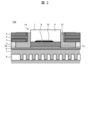
- FIG. 2 is a cross-sectional view taken along line A-A' in FIG. 1;
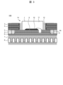
- FIG. FIG. 2 is a cross-sectional view taken along the line B-B' of FIG. 1;
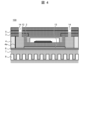
- FIG. 4 is a first modified example of FIG. 3 ;
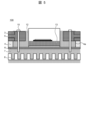
- FIG. 4 is a second example of FIG. 3;
- FIG. 4 is a third modified example of FIG. 3;
- a substrate-integrated semiconductor module 100 is a circuit module that constitutes a power conversion circuit of a power converter.
- a semiconductor module 100 has a circuit body 1 , a power wiring layer 3 , a heat dissipation member 4 and a substrate 5 .
- the board 5 is a resin printed board (control circuit board).
- a heat radiating member 4 is formed in a sheet shape on the substrate 5 and is arranged so as to surround each circuit body 1 .
- the power wiring layer 3 is connected to the circuit bodies 1 via the external terminals 2 of each circuit body 1 .
- the heat dissipating member 4 is sheet-like is that a large amount of the heat dissipating member 4 is required corresponding to the amount of current in the main circuit section of the power converter.
- the frame portion 4a is formed around the circuit body 1 and the external terminals 2 of the circuit body 1 by a large amount of the heat radiating member 4, so that the filling member filled around the circuit body 1 is filled. Leakage can be prevented.
- the power wiring layer 3 is formed on the upper and lower surfaces of the substrate 5 .
- the circuit body 1 is arranged on the inner peripheral side of the through hole 14 provided in the substrate 5 .
- the side surface of the circuit body 1 is fixed to the substrate 5 via the insulating filling member 12, so that the vibration resistance is improved.
- the circuit body 1 has a conductive member 9 and a semiconductor element 10 , each of which is covered with a sealing resin 11 . As a result, the semiconductor element 10 and the conductive member 9 are insulated from surrounding electrical components and protected from foreign matter.
- an IGBT (Insulated Gate Bipolar Transistor) element, a MOSFET (metal-oxide-semiconductor field-effect transistor) element, a diode element, or the like is used as the semiconductor element 10.
- the semiconductor element 10 is electrically connected to the conductive member 9 via a connection wiring such as a bonding wire or a bonding material such as solder.
- the conductive member 9 has external terminals 2 that connect the circuit body 1 to electrical components such as the substrate 5 .
- the external terminals 2 are connected to the semiconductor element 10 and electrically connected to the power wiring layer 3 (lower side in the figure) of the substrate 5 by a bonding material such as solder.
- the substrate 5 is composed of the power wiring layer 3 and an insulating resin layer.
- the circuit body 1 is connected to other electrical components (not shown) through the external terminals 2 and the substrate 5 to form a power conversion circuit.
- a filling member 12 is filled so as to cover the connecting portions between the circuit body 1 and the external terminals 2 and the power wiring layer 3 through the through holes 14 formed in the substrate 5 .
- the filling member 12 is an insulating material such as resin, and when filled, insulates between the external terminal 2 of the circuit body 1 and between the power wiring layer 3 and the cooler 7 .
- the filling state of the filling member 12 presence or absence of air bubbles, filling rate, etc.
- the reliability of the filling result of the filling member 12 is high. can be improved.
- a heat transfer member 13 is provided below the conductive member 9, and an insulating member 6 is provided further below.
- the insulating member 6 is composed of a ceramic substrate, an insulating resin sheet, or the like, and is fixed to the cooler 7 by brazing or crimping.
- the insulating member 6 is in contact with the heat radiating member 4 , the filling member 12 and the heat transfer member 13 at its upper side.
- the heat dissipation member 4 is in contact with the power wiring layer 3 on the lower side of the substrate 5 . That is, the heat radiating member 4 is arranged between the substrate 5 and the cooler 7 , and the power wiring layer 3 and the cooler 7 are in contact with each other through the heat radiating member 4 and the insulating member 6 .
- the power wiring layer 3 can dissipate heat to the coolant 8 flowing inside the cooler 7, and the temperature of the substrate 5 is reduced.
- the heat radiating member 4 is made of a resin sheet or the like having high thermal conductivity and elasticity (stretchability) capable of following the steps and warpage of the substrate 5 .
- the insulating member 6 is arranged between the cooler 7 and the circuit body 1 and between the cooler 7 and the board 5 to insulate between the cooler 7 and the circuit body 1 and between the cooler 7 and the board 5 .
- the heat dissipation member 4 is formed on the cooler 7, the cooling effect of the circuit body 1 is enhanced through the filling member 12 filled in the inner region (the region surrounded by the frame portion 4a). be able to.
- the area surrounded by the heat radiating member 4 forming the frame portion 4a on the insulating member 6 on the bottom surface is filled with the filling member 12 from the through hole 14 without any gap as described above, and the circuit body 1 is mounted.
- a filling member 12 is filled so as to surround the outer periphery of the area.
- the filling member 12 functions as a potting mold for the circuit body 1, and while the insulating coating material (filling member 12) is prevented from flowing out, the circuit body 1 is reliably insulated from the substrate 5 and the power wiring layer 3. be done. Therefore, it becomes possible to use a low-viscosity filling member 12 at the time of filling, and the filling process becomes easier than before.
- a low-viscosity filling member is used, bubbles generated in the filling member 12 can be easily eliminated, and by suppressing the inclusion of bubbles, the insulation reliability of the semiconductor module 100 can be improved.
- the filling member 12 is filled on the inner peripheral side of the frame portion 4a formed by the sheet-shaped heat radiating member 4. As shown in FIG. As a result, the necessary insulating distance between the external terminals 2 projecting from the same direction of the circuit body 1 and having different potentials is shortened, so that the external terminals 2 can be brought close to each other.
- the entire integrated semiconductor module 100 can be miniaturized.
- the cooler 7 is arranged as a cooler for the circuit body 1 and the substrate 5, and cools the circuit body 1 and the substrate 5 via the heat transfer member 13, the heat radiation member 4, or the insulating member 6.
- the cooler 7 is made of a material with excellent thermal conductivity, such as aluminum or copper. Since the cooler 7 has fins or pins on the surface that contacts the coolant 8 , the surface area that contacts the coolant 8 can be increased, and the cooling performance of the cooler 7 can be improved.
- the coolant 8 is liquid such as cooling water, and is pressure-fed from the outside to the flow path of the cooler 7 by a pump (not shown) and flows through the internal flow path of the cooler 7 .
- the external terminals 2 and the power wiring layer 3 are arranged so that their parts are in contact with each other (Fig. 3).
- the reason for this arrangement is that the width of the wiring layer 3 of the substrate 5 varies depending on the amount of current applied when making an actual circuit. This is because it is necessary to improve the degree of freedom of arrangement of 1. Therefore, a countermeasure is considered to prevent component displacement at the contact portion with the external terminal 2 by making the power wiring layer 3 partially thin and forming a stepped portion, while leaving the layer of the external terminal 2 as it is. can.
- the circuit body 1 (external terminals 2) and the substrate 5 may be vertically shifted from each other in consideration of design convenience when arranging them.
- the substrate 5 has a through-hole 14 , and is shaped to serve as a lid for the circuit body 1 by disposing a part of the substrate 5 so as to cover the circuit body 1 . Further, the through hole 14 is arranged on the inner peripheral side of the frame portion 4a formed by the heat radiating member 4. As shown in FIG. This facilitates adjustment of the filling amount of the filling member 12 and improves the reliability of setting the filling member 12 to an appropriate amount. Also, by providing a plurality of through-holes 14, the filling speed can be improved and the removal of air bubbles can be facilitated.
- the fixing member 15 fastens the substrate 5 and the cooler 7 through a fixing hole provided in the substrate 5 and a fixing hole provided in the cooler 7 for passing the fixing member 15 .
- a bolt, a screw, or the like is used as the fixing member 15 .
- the fixing member 15 is arranged on the inner peripheral side of the frame portion 4 a formed by the heat radiating member 4 . By arranging the fixing member 15 near the heat radiating member 4, it is possible to improve the adhesion between the substrate 5 and the heat radiating member 4 and between the insulating member 6 and the heat radiating member 4, thereby suppressing the outflow of the filling member 12. can be done. Further, the through hole 14 of the insulating member 6 generated (formed) by the fixing member 15 is filled with the filling member 12, and the cooler 7 and the substrate 5 are insulated, and the cooler 7 and the circuit body 1 are each insulated.
- the cooler 7 is arranged not only on the lower surface of the circuit body 1 but also on the upper surface thereof, and cools both sides of the semiconductor element 10 of the circuit body 1 .
- the cooler arranged on the upper surface is a cooler 7a.
- the second insulating member 6a in contact with the cooler 7a is made of a ceramic substrate, an insulating resin sheet, or the like, and is fixed to the second cooler 7a by brazing or crimping.
- the second insulating member 6a is arranged between the second cooler 7a and the circuit body 1, and between the second cooler 7a and the substrate 5, so that the second cooler 7a and the circuit body 1 and the second cooler 7a and the substrate 5 are insulated from each other.
- the second heat transfer member 13a is arranged between the circuit body 1 and the second insulating member 6a, and heat dissipation grease or the like having high heat conductivity and capable of suppressing contact heat resistance is used.
- the second cooler 7a is arranged at a position not overlapping the through hole 14 of the substrate 5 filled with the filling member 12 .
- the filling member 12 can be filled with the cooler 7 and the second cooler 7a attached to the substrate 5 and the circuit body 1, and the filling state of the filling member 12 can be visually confirmed.
- the semiconductor module 100 includes a circuit body 1 having a semiconductor element 10 and a plurality of external terminals 2 connected to the semiconductor element 10, and a substrate having a power wiring layer 3 connected to the plurality of external terminals 2. 5, an insulating filling member 12 covering the connecting portions between the plurality of external terminals 2 and the power wiring layer 3, a cooler 7 on which the circuit body 1 and the substrate 5 are mounted on one surface side, and a cooler 7 and a heat dissipating member 4 arranged between the substrate 5, the heat dissipating member 4 forming a frame portion 4a so as to surround the outer periphery of the area where the circuit body 1 is mounted on the cooler 7, The inner peripheral side of the frame portion 4a is filled with the filling member 4. As shown in FIG. By doing so, it is possible to provide the semiconductor module 100 that achieves both improved cooling performance of the substrate 5 and increased wiring density of the terminal portion.
- the substrate 5 has a through hole 14 for filling the filling member 12 on the inner peripheral side of the frame portion 4a.
- the circuit body 1 is arranged inside the through hole 14 provided in the substrate. By doing so, the circuit body 1 is insulated from surrounding electrical components and protected from foreign matter by the filling member 12 that fills the through holes 14 .
- the substrate 5 has a shape that serves as a lid for the circuit body 1, and the filling member 12 from the through holes 14 provided in the remaining substrate 5 is easily filled, and the reliability of the filling result is increased. improve sexuality.
- a fixing member 15 for fastening the substrate 5 and the cooler 7 is provided, and the fixing member 15 is arranged on the inner peripheral side of the frame portion 4a. By doing so, it is possible to improve the adhesion between the substrate 5 and the heat radiating member 4 and between the insulating member 6 and the heat radiating member 4 , thereby suppressing the outflow of the filling member 12 . Further, the through hole 14 of the insulating member 6 generated (formed) by the fixing member 15 is filled with the filling member 12, and the cooler 7 and the substrate 5 are insulated, and the cooler 7 and the circuit body 1 are each insulated.
- a second cooler 7 a is provided on the upper surface of the circuit body 1 , and the second cooler 7 a is arranged at a position not overlapping the through hole 14 of the substrate 5 filled with the filling member 12 . Since the circuit body 1 is also cooled from the upper surface by doing so, the temperature rise of the semiconductor element inside the circuit body 1 is further suppressed, and the reliability of the circuit body 1 is improved. In addition, the filling member 12 can be filled with the cooler 7 and the second cooler 7a attached to the substrate 5 and the circuit body 1, and the filling state of the filling member 12 can be visually confirmed.
- the present invention is not limited to the above embodiments, and various modifications and other configurations can be combined without departing from the scope of the invention. Moreover, the present invention is not limited to those having all the configurations described in the above embodiments, and includes those having some of the configurations omitted.
- circuit body 2 external terminal 3: power wiring layer 4: heat dissipation member 4a: frame 5: substrate 6: insulating member 6a: second insulating member 7: cooler 7a: second cooler 8: refrigerant 9: conductive Thermal member 10: Semiconductor element 11: Sealing resin 12: Filling member 13: Heat transfer member 13a: Second heat transfer member 14: Through hole 15: Fixing member 100: Substrate integrated semiconductor module
Landscapes
- Engineering & Computer Science (AREA)
- Power Engineering (AREA)
- Cooling Or The Like Of Semiconductors Or Solid State Devices (AREA)
- Inverter Devices (AREA)
Abstract
Description
以下、図面を参照して本発明の実施形態を説明する。以下の記載および図面は、本発明を説明するための例示であって、説明の明確化のため、適宜、省略および簡略化がなされている。本発明は、他の種々の形態でも実施する事が可能である。特に限定しない限り、各構成要素は単数でも複数でも構わない。
基板一体型の半導体モジュール100は、電力変換装置の電力変換回路を構成する回路モジュールである。半導体モジュール100は、回路体1、電力配線層3、放熱部材4、基板5を有している。基板5は、樹脂状のプリント基板(制御回路基板)である。基板5の上には放熱部材4がシート状に形成されており、それぞれの回路体1を囲うような配置である。電力配線層3は、それぞれの回路体1が有する外部端子2を介して回路体1に接続している。
電力配線層3は、基板5の上下面に形成されている。回路体1は、基板5に設けられた貫通孔14の内周側に配置されている。回路体1は、絶縁性の充填部材12を介してその側面が基板5に固定されていることで、耐振性が向上している。回路体1は、導電性部材9、半導体素子10、を有しており、それぞれが封止樹脂11で覆われている。これにより、半導体素子10と導電性部材9が周囲の電気部品に対して絶縁されるとともに、異物から保護される。
(図4)
基板5は、貫通孔14を有し、基板5の一部が回路体1を覆うように配置されることで、回路体1に対して蓋になるような形状である。また、貫通孔14は、放熱部材4により形成される枠部4aの内周側に配置される。これにより、充填部材12の充填量の調整が容易になり、充填部材12を適量にする信頼度が向上する。また複数の貫通孔14を設けることにより充填速度を向上させ、さらに気泡の除去が容易となる。
(図5)
固定部材15は、固定部材15を通すために基板5に設けられた固定穴と冷却器7に設けられた固定穴とを通して、基板5と冷却器7を締結する。固定部材15はボルトやねじなどが用いられる。固定部材15は、放熱部材4により形成される枠部4aの内周側に配置される。固定部材15は、放熱部材4の近傍に配置することによって、基板5と放熱部材4および絶縁部材6と放熱部材4の密着性を向上させることが可能となり、充填部材12の流出を抑制することができる。また、固定部材15により生じる(形成される)絶縁部材6の貫通孔14が充填部材12により充填され、冷却器7と基板5および冷却器7と回路体1はそれぞれ絶縁される。
(図6)
冷却器7は、回路体1の下面だけでなく上面にも配置され、回路体1の半導体素子10を両面冷却する。上面に配置された冷却器は冷却器7aとする。冷却器7aと接している第2絶縁部材6aは、セラミック基板や絶縁樹脂シートなどにより構成され、第2冷却器7aにろう付けや圧着により固定される。第2絶縁部材6aは、第2冷却器7aと回路体1、および第2冷却器7aと基板5との間に配置されることで、第2冷却器7aと回路体1および第2冷却器7aと基板5との間をそれぞれ絶縁する。第2伝熱部材13aは、回路体1と第2絶縁部材6aの間に配置され、熱伝導率が高く、接触熱抵抗も抑制できる放熱グリスなどが用いられる。第2冷却器7aは、充填部材12が充填される基板5の貫通孔14と重ならない位置に配置される。
2:外部端子
3:電力配線層
4:放熱部材
4a:枠部
5:基板
6:絶縁部材
6a:第2絶縁部材
7:冷却器
7a:第2冷却器
8:冷媒
9:導電性部材
10:半導体素子
11:封止樹脂
12:充填部材
13:伝熱部材
13a:第2伝熱部材
14:貫通孔
15:固定部材
100:基板一体半導体モジュール
Claims (6)
- 半導体素子と、前記半導体素子と接続される複数の外部端子と、を有する回路体と、
前記複数の外部端子と接続される電力配線層を有する基板と、
前記複数の外部端子と前記電力配線層との接続部を覆う絶縁性の充填部材と、
一方の面側に前記回路体および前記基板が搭載される冷却器と、
前記冷却器と前記基板との間に配置される放熱部材と、を備え、
前記放熱部材は、前記冷却器上において、前記回路体が搭載される領域の外周を囲むように枠部を形成し、
前記枠部の内周側には、前記充填部材が充填される
半導体モジュール。 - 請求項1に記載の半導体モジュールであって、
前記基板は、前記枠部の内周側に前記充填部材を充填するための貫通孔を有する
半導体モジュール。 - 請求項2に記載の半導体モジュールであって、
前記回路体が前記基板に設けられた前記貫通孔の内側に配置された
半導体モジュール。 - 請求項3に記載の半導体モジュールであって、
前記基板の一部が前記回路体を覆うように配置された
半導体モジュール。 - 請求項1に記載の半導体モジュールであって、
前記基板と前記冷却器とを締結する固定部材を備え、
前記固定部材は、前記枠部の内周側に配置された
半導体モジュール。 - 請求項1に記載の半導体モジュールであって、
前記回路体の上面には第2冷却器を備え、
前記第2冷却器は、前記充填部材が充填される前記基板の貫通孔とは重ならない位置に配置される
半導体モジュール。
Priority Applications (2)
| Application Number | Priority Date | Filing Date | Title |
|---|---|---|---|
| CN202280070556.0A CN118140303A (zh) | 2021-10-26 | 2022-10-19 | 半导体模块 |
| US18/702,558 US20250279329A1 (en) | 2021-10-26 | 2022-10-19 | Semiconductor module |
Applications Claiming Priority (2)
| Application Number | Priority Date | Filing Date | Title |
|---|---|---|---|
| JP2021175054A JP7760333B2 (ja) | 2021-10-26 | 2021-10-26 | 半導体モジュール |
| JP2021-175054 | 2021-10-26 |
Publications (1)
| Publication Number | Publication Date |
|---|---|
| WO2023074501A1 true WO2023074501A1 (ja) | 2023-05-04 |
Family
ID=86159405
Family Applications (1)
| Application Number | Title | Priority Date | Filing Date |
|---|---|---|---|
| PCT/JP2022/038966 Ceased WO2023074501A1 (ja) | 2021-10-26 | 2022-10-19 | 半導体モジュール |
Country Status (4)
| Country | Link |
|---|---|
| US (1) | US20250279329A1 (ja) |
| JP (1) | JP7760333B2 (ja) |
| CN (1) | CN118140303A (ja) |
| WO (1) | WO2023074501A1 (ja) |
Citations (5)
| Publication number | Priority date | Publication date | Assignee | Title |
|---|---|---|---|---|
| JPH07312411A (ja) * | 1994-05-18 | 1995-11-28 | Hitachi Ltd | 電子装置 |
| JP2003249599A (ja) * | 2002-02-18 | 2003-09-05 | Phoenix Precision Technology Corp | 支持効果を有するヒートシンク装置をチップキャリアに応用する方法 |
| JP2006186057A (ja) * | 2004-12-27 | 2006-07-13 | Fujitsu Ltd | 半導体装置及びその製造方法 |
| JP2013026296A (ja) * | 2011-07-19 | 2013-02-04 | Daikin Ind Ltd | パワーモジュール |
| WO2020105556A1 (ja) * | 2018-11-21 | 2020-05-28 | 三菱電機株式会社 | 半導体装置、電力変換装置及び半導体装置の製造方法 |
Family Cites Families (2)
| Publication number | Priority date | Publication date | Assignee | Title |
|---|---|---|---|---|
| JP5570476B2 (ja) * | 2011-07-05 | 2014-08-13 | 三菱電機株式会社 | 半導体装置および半導体装置の製造方法 |
| JP7153538B2 (ja) | 2018-11-16 | 2022-10-14 | 日立Astemo株式会社 | パワー半導体モジュール、電力変換装置およびパワー半導体モジュールの製造方法 |
-
2021
- 2021-10-26 JP JP2021175054A patent/JP7760333B2/ja active Active
-
2022
- 2022-10-19 WO PCT/JP2022/038966 patent/WO2023074501A1/ja not_active Ceased
- 2022-10-19 US US18/702,558 patent/US20250279329A1/en active Pending
- 2022-10-19 CN CN202280070556.0A patent/CN118140303A/zh active Pending
Patent Citations (5)
| Publication number | Priority date | Publication date | Assignee | Title |
|---|---|---|---|---|
| JPH07312411A (ja) * | 1994-05-18 | 1995-11-28 | Hitachi Ltd | 電子装置 |
| JP2003249599A (ja) * | 2002-02-18 | 2003-09-05 | Phoenix Precision Technology Corp | 支持効果を有するヒートシンク装置をチップキャリアに応用する方法 |
| JP2006186057A (ja) * | 2004-12-27 | 2006-07-13 | Fujitsu Ltd | 半導体装置及びその製造方法 |
| JP2013026296A (ja) * | 2011-07-19 | 2013-02-04 | Daikin Ind Ltd | パワーモジュール |
| WO2020105556A1 (ja) * | 2018-11-21 | 2020-05-28 | 三菱電機株式会社 | 半導体装置、電力変換装置及び半導体装置の製造方法 |
Also Published As
| Publication number | Publication date |
|---|---|
| CN118140303A (zh) | 2024-06-04 |
| JP7760333B2 (ja) | 2025-10-27 |
| US20250279329A1 (en) | 2025-09-04 |
| JP2023064653A (ja) | 2023-05-11 |
Similar Documents
| Publication | Publication Date | Title |
|---|---|---|
| US8637979B2 (en) | Semiconductor device | |
| US7190581B1 (en) | Low thermal resistance power module assembly | |
| US12218037B2 (en) | Semiconductor device | |
| JP7735655B2 (ja) | 半導体装置 | |
| JP6093455B2 (ja) | 半導体モジュール | |
| US10163752B2 (en) | Semiconductor device | |
| US12400930B2 (en) | Power module package | |
| JP2019071392A (ja) | 半導体装置 | |
| JP4465906B2 (ja) | パワー半導体モジュール | |
| US11195775B2 (en) | Semiconductor module, semiconductor device, and manufacturing method of semiconductor module | |
| CN114730748B (zh) | 用于消耗装置的可控电功率供应的具有被封装的功率半导体的功率模块及用于生产该功率模块的方法 | |
| JP7367309B2 (ja) | 半導体モジュール、半導体装置及び半導体装置の製造方法 | |
| US12489031B2 (en) | Semiconductor device and manufacturing method thereof | |
| JP2022087498A (ja) | 冷却器及び半導体装置 | |
| WO2022215357A1 (ja) | 半導体装置 | |
| CN112530915A (zh) | 半导体装置 | |
| US12191218B2 (en) | Semiconductor device including surface pressure absorbing member for fastening heat sink | |
| JP2017054855A (ja) | 半導体装置、及び半導体パッケージ | |
| JP2017054842A (ja) | 配線基板、半導体装置、及び半導体パッケージ | |
| JP7103256B2 (ja) | 半導体装置 | |
| US20240057303A1 (en) | Semiconductor cooling arrangement with improved heatsink | |
| JP2023134143A (ja) | 半導体モジュール、半導体装置、及び車両 | |
| JP2010177619A (ja) | 半導体モジュール | |
| JP7392319B2 (ja) | 半導体装置 | |
| US20250192061A1 (en) | Semiconductor Module and Power Conversion Device |
Legal Events
| Date | Code | Title | Description |
|---|---|---|---|
| 121 | Ep: the epo has been informed by wipo that ep was designated in this application |
Ref document number: 22886829 Country of ref document: EP Kind code of ref document: A1 |
|
| WWE | Wipo information: entry into national phase |
Ref document number: 18702558 Country of ref document: US |
|
| WWE | Wipo information: entry into national phase |
Ref document number: 202280070556.0 Country of ref document: CN |
|
| NENP | Non-entry into the national phase |
Ref country code: DE |
|
| 122 | Ep: pct application non-entry in european phase |
Ref document number: 22886829 Country of ref document: EP Kind code of ref document: A1 |
|
| WWP | Wipo information: published in national office |
Ref document number: 18702558 Country of ref document: US |