WO2023074230A1 - 撮像装置 - Google Patents
撮像装置 Download PDFInfo
- Publication number
- WO2023074230A1 WO2023074230A1 PCT/JP2022/035984 JP2022035984W WO2023074230A1 WO 2023074230 A1 WO2023074230 A1 WO 2023074230A1 JP 2022035984 W JP2022035984 W JP 2022035984W WO 2023074230 A1 WO2023074230 A1 WO 2023074230A1
- Authority
- WO
- WIPO (PCT)
- Prior art keywords
- electrode
- photoelectric conversion
- semiconductor material
- injection layer
- charge injection
- Prior art date
- Legal status (The legal status is an assumption and is not a legal conclusion. Google has not performed a legal analysis and makes no representation as to the accuracy of the status listed.)
- Ceased
Links
Images


Classifications
-
- H—ELECTRICITY
- H10—SEMICONDUCTOR DEVICES; ELECTRIC SOLID-STATE DEVICES NOT OTHERWISE PROVIDED FOR
- H10K—ORGANIC ELECTRIC SOLID-STATE DEVICES
- H10K39/00—Integrated devices, or assemblies of multiple devices, comprising at least one organic radiation-sensitive element covered by group H10K30/00
- H10K39/30—Devices controlled by radiation
- H10K39/32—Organic image sensors
-
- H—ELECTRICITY
- H10—SEMICONDUCTOR DEVICES; ELECTRIC SOLID-STATE DEVICES NOT OTHERWISE PROVIDED FOR
- H10F—INORGANIC SEMICONDUCTOR DEVICES SENSITIVE TO INFRARED RADIATION, LIGHT, ELECTROMAGNETIC RADIATION OF SHORTER WAVELENGTH OR CORPUSCULAR RADIATION
- H10F39/00—Integrated devices, or assemblies of multiple devices, comprising at least one element covered by group H10F30/00, e.g. radiation detectors comprising photodiode arrays
- H10F39/10—Integrated devices
- H10F39/12—Image sensors
-
- H—ELECTRICITY
- H10—SEMICONDUCTOR DEVICES; ELECTRIC SOLID-STATE DEVICES NOT OTHERWISE PROVIDED FOR
- H10K—ORGANIC ELECTRIC SOLID-STATE DEVICES
- H10K30/00—Organic devices sensitive to infrared radiation, light, electromagnetic radiation of shorter wavelength or corpuscular radiation
- H10K30/30—Organic devices sensitive to infrared radiation, light, electromagnetic radiation of shorter wavelength or corpuscular radiation comprising bulk heterojunctions, e.g. interpenetrating networks of donor and acceptor material domains
- H10K30/353—Organic devices sensitive to infrared radiation, light, electromagnetic radiation of shorter wavelength or corpuscular radiation comprising bulk heterojunctions, e.g. interpenetrating networks of donor and acceptor material domains comprising blocking layers, e.g. exciton blocking layers
-
- H—ELECTRICITY
- H10—SEMICONDUCTOR DEVICES; ELECTRIC SOLID-STATE DEVICES NOT OTHERWISE PROVIDED FOR
- H10K—ORGANIC ELECTRIC SOLID-STATE DEVICES
- H10K30/00—Organic devices sensitive to infrared radiation, light, electromagnetic radiation of shorter wavelength or corpuscular radiation
- H10K30/60—Organic devices sensitive to infrared radiation, light, electromagnetic radiation of shorter wavelength or corpuscular radiation in which radiation controls flow of current through the devices, e.g. photoresistors
-
- H—ELECTRICITY
- H10—SEMICONDUCTOR DEVICES; ELECTRIC SOLID-STATE DEVICES NOT OTHERWISE PROVIDED FOR
- H10K—ORGANIC ELECTRIC SOLID-STATE DEVICES
- H10K30/00—Organic devices sensitive to infrared radiation, light, electromagnetic radiation of shorter wavelength or corpuscular radiation
- H10K30/80—Constructional details
- H10K30/84—Layers having high charge carrier mobility
- H10K30/85—Layers having high electron mobility, e.g. electron-transporting layers or hole-blocking layers
-
- Y—GENERAL TAGGING OF NEW TECHNOLOGICAL DEVELOPMENTS; GENERAL TAGGING OF CROSS-SECTIONAL TECHNOLOGIES SPANNING OVER SEVERAL SECTIONS OF THE IPC; TECHNICAL SUBJECTS COVERED BY FORMER USPC CROSS-REFERENCE ART COLLECTIONS [XRACs] AND DIGESTS
- Y02—TECHNOLOGIES OR APPLICATIONS FOR MITIGATION OR ADAPTATION AGAINST CLIMATE CHANGE
- Y02E—REDUCTION OF GREENHOUSE GAS [GHG] EMISSIONS, RELATED TO ENERGY GENERATION, TRANSMISSION OR DISTRIBUTION
- Y02E10/00—Energy generation through renewable energy sources
- Y02E10/50—Photovoltaic [PV] energy
- Y02E10/549—Organic PV cells
Definitions
- the present disclosure relates to an imaging device using photoelectric conversion elements.
- Organic semiconductor materials have physical properties and functions not found in conventional inorganic semiconductor materials such as silicon, and are being actively researched as semiconductor materials that can realize new semiconductor devices and electronic equipment.
- photoelectric conversion elements that use organic semiconductor materials as materials for the photoelectric conversion layer.
- the photoelectric conversion element When the photoelectric conversion element is irradiated with light, pairs of electrons and holes called excitons are generated. As shown in Non-Patent Document 1, the generated excitons reach the interface between the donor material and the acceptor material by diffusing over a distance of approximately 5 nm to 20 nm, causing charge separation to generate electrons and holes. occurs.
- the interface between the donor material and the acceptor material is also called the donor-acceptor interface.
- a photoelectric conversion element can be used as an imaging device or the like by extracting generated electrons or holes as signal charges. In order to improve the sensitivity of a photoelectric conversion element used in an imaging device or the like, it is desired to efficiently generate electric charge and take it out to an electrode.
- Patent Document 1 proposes a method of providing a charge blocking layer and a charge transport auxiliary layer in a photoelectric conversion element.
- This charge blocking layer is provided between the electrode and the photoelectric conversion layer.
- the charge blocking layer prevents backflow of charges from the electrodes when a bias voltage is applied to the photoelectric conversion element.
- the charge transport assisting layer is provided between the charge blocking layer and the photoelectric conversion layer, and assists in transporting electrons or holes generated by photoelectric conversion to the electrode.
- an object of the present disclosure is to provide an imaging device with improved sensitivity.
- An imaging device includes a first electrode, a second electrode facing the first electrode, and a donor semiconductor material and an acceptor positioned between the first electrode and the second electrode. a photoelectric conversion layer for generating pairs of electrons and holes, a charge injection layer positioned between the first electrode and the photoelectric conversion layer, and electrically connected to the second electrode. and a charge accumulation region for accumulating the holes.
- the ionization potential of the charge injection layer is lower than the ionization potential of the acceptor semiconductor material.
- the electron affinity of the charge injection layer is lower than the electron affinity of the acceptor semiconductor material.
- the light transmittance of the charge injection layer is 70% or more.
- An imaging device includes a first electrode, a second electrode facing the first electrode, and a donor semiconductor material positioned between the first electrode and the second electrode. and an acceptor semiconductor material, the photoelectric conversion layer generating pairs of electrons and holes, the charge injection layer positioned between the first electrode and the photoelectric conversion layer, and the second electrode electrically connected to the and a charge storage region for storing the electrons.
- the electron affinity of the charge injection layer is greater than or equal to the electron affinity of the donor semiconductor material.
- the ionization potential of the charge injection layer is higher than the ionization potential of the donor semiconductor material.
- the light transmittance of the charge injection layer is 70% or more.
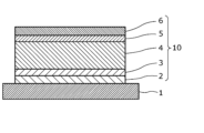
- FIG. 1 is a schematic cross-sectional view showing the configuration of a photoelectric conversion element according to an embodiment.
- FIG. 2 is an exemplary energy band diagram in the photoelectric conversion device shown in FIG.
- FIG. 3 is a diagram illustrating an example of the circuit configuration of the imaging device according to the embodiment;
- FIG. 4 is a schematic cross-sectional view showing the device structure of a pixel in the imaging device according to the embodiment.
- FIG. 5 is an exemplary energy band diagram in another photoelectric conversion element according to the embodiment.
- Patent Document 1 has the following problems.
- the diffusion length of excitons in organic semiconductors is about 5 nm to 20 nm.
- the exciton is deactivated and is not photoelectrically converted.
- part of the excitons generated in the region near the charge-transporting assisting layer in the organic photoelectric conversion layer is scattered by the charge-transporting assisting layer and reaches the donor-acceptor interface. can't That is, although the transport efficiency of excitons after charge separation is improved by providing the charge transport assisting layer, the charge separation efficiency is not improved.
- the present disclosure has been made based on such findings, and improves sensitivity by efficiently separating excitons generated near the interface between the photoelectric conversion layer and other layers in the photoelectric conversion layer.
- An imaging device includes a first electrode, a second electrode facing the first electrode, and a donor semiconductor material and an acceptor positioned between the first electrode and the second electrode. a photoelectric conversion layer for generating pairs of electrons and holes, a charge injection layer positioned between the first electrode and the photoelectric conversion layer, and electrically connected to the second electrode. and a charge accumulation region for accumulating the holes.
- the ionization potential of the charge injection layer is lower than the ionization potential of the acceptor semiconductor material.
- the electron affinity of the charge injection layer is lower than the electron affinity of the acceptor semiconductor material.
- the light transmittance of the charge injection layer is 70% or more.
- photoelectric conversion occurs due to charge separation between the acceptor semiconductor material contained in the photoelectric conversion layer and the material contained in the charge injection layer, and the sensitivity of the imaging device can be improved.
- excitons generated by light absorption by the acceptor semiconductor material and the charge injection layer contained in the photoelectric conversion layer diffuse to the interface with the charge injection layer. Due to the above relationship between the energy band of the charge injection layer and the energy band of the acceptor semiconductor material, electrons remain in the acceptor semiconductor material, holes move to the charge injection layer, and exciton electrons Pairs with holes separate at the interface.
- the charge injection layer can suppress charge injection from the first electrode to the photoelectric conversion layer, noise signals that adversely affect the SN ratio can be reduced.
- the charge injection layer becomes less likely to absorb light, and the excitons generated in the charge injection layer diffuse and reach the interface with the acceptor material of the photoelectric conversion layer, thereby improving the sensitivity of the imaging device. and can be made compatible.
- the volume ratio of the acceptor semiconductor material in the photoelectric conversion layer may be 70% or more.
- the contact interface between the acceptor semiconductor material and the charge injection layer, where charge separation of excitons occurs increases, and the sensitivity of the imaging device can be further improved.
- the imaging device further includes a charge blocking layer positioned between the second electrode and the photoelectric conversion layer, and subtracts the ionization potential of the charge injection layer from the ionization potential of the donor semiconductor material.
- the value may be smaller than the ionization potential of the charge blocking layer minus the ionization potential of the donor semiconductor material.
- an imaging device includes a first electrode, a second electrode facing the first electrode, and positioned between the first electrode and the second electrode; a photoelectric conversion layer that includes a semiconductor material and an acceptor semiconductor material and generates pairs of electrons and holes, a charge injection layer positioned between the first electrode and the photoelectric conversion layer, and a second electrode; a charge storage region electrically connected to store the electrons.
- the electron affinity of the charge injection layer is greater than or equal to the electron affinity of the donor semiconductor material.
- the ionization potential of the charge injection layer is higher than the ionization potential of the donor semiconductor material.
- the light transmittance of the charge injection layer is 70% or more.
- photoelectric conversion occurs between the donor semiconductor material contained in the photoelectric conversion layer and the material contained in the charge injection layer, and the sensitivity of the imaging device can be improved.
- excitons generated by light absorption of the donor semiconductor material contained in the photoelectric conversion layer diffuse to the interface with the charge injection layer. Due to the above relationship between the energy band of the charge injection layer and the energy band of the donor semiconductor material, holes remain in the donor semiconductor material, electrons move to the charge injection layer, and exciton electrons Pairs with holes separate at the interface. Electrons separated by a voltage or the like applied between the first electrode and the second electrode conduct hopping conduction in the photoelectric conversion layer, are collected by the second electrode, and are accumulated in the charge accumulation region.
- electrons separated at the interface between the donor semiconductor material and the charge injection layer can also be used as signal charges, so that the sensitivity of the imaging device can be improved.
- the charge injection layer can suppress charge injection from the first electrode to the photoelectric conversion layer, noise signals that adversely affect the SN ratio can be reduced.
- the volume ratio of the donor semiconductor material in the photoelectric conversion layer may be 70% or more.
- the contact interface between the donor semiconductor material and the charge injection layer, where charge separation of excitons occurs increases, making it possible to further improve the sensitivity of the imaging device.
- the imaging device further includes a charge blocking layer positioned between the second electrode and the photoelectric conversion layer, and subtracts the electron affinity of the charge injection layer from the electron affinity of the acceptor semiconductor material.
- the value may be greater than the electron affinity of the charge blocking layer minus the electron affinity of the acceptor semiconductor material.
- the rate-determining barrier occurs when the electrons hop from the charge injection layer to the donor semiconductor material of the photoelectric conversion layer. electrons are collected efficiently.
- the charge blocking layer can suppress injection of charges from the second electrode to the photoelectric conversion layer, noise signals that adversely affect the SN ratio can be reduced.
- the charge injection layer may have a light transmittance of 70% or more in the visible light region.
- the thickness of the charge injection layer may be 5 nm or more.
- the thickness of the charge injection layer may be less than 20 nm.
- an imaging device includes a first electrode, a second electrode facing the first electrode, a donor positioned between the first electrode and the second electrode, and a donor a photoelectric conversion layer for generating pairs of electrons and holes, a charge injection layer positioned between the first electrode and the photoelectric conversion layer, and the second electrode. a charge storage region electrically connected to and storing the holes.
- the ionization potential of the charge injection layer is lower than the ionization potential of the acceptor semiconductor material.
- the electron affinity of the charge injection layer is lower than the electron affinity of the acceptor semiconductor material.
- the thickness of the charge injection layer is greater than or equal to 5 nm and less than 20 nm.
- the charge injection layer becomes less likely to absorb light, and the excitons generated in the charge injection layer diffuse and reach the interface between the photoelectric conversion layer and the acceptor material, thereby improving the sensitivity of the imaging device. and can be compatible.
- the terms “upper” and “lower” do not refer to the upward direction (vertically upward) and the downward direction (vertically downward) in absolute spatial recognition, but are based on the stacking order in the stacking structure. It is used as a term defined by a relative positional relationship. Note that terms such as “upper” and “lower” are used only to specify the mutual arrangement of members, and are not intended to limit the orientation of the imaging apparatus when it is used. Also, the terms “above” and “below” are used only when two components are spaced apart from each other and there is another component between them, as well as when two components are spaced apart from each other. It also applies when two components are in contact with each other and are placed in close contact with each other.
- FIG. 1 is a schematic cross-sectional view showing the configuration of a photoelectric conversion element 10 according to this embodiment.
- a photoelectric conversion element 10 is supported by a support substrate 1 and positioned between a pair of electrodes, upper electrode 6 and lower electrode 2, and upper electrode 6 and lower electrode 2.
- the upper electrode 6 is an example of a first electrode
- the lower electrode 2 is an example of a second electrode.
- the photoelectric conversion element 10 is used, for example, in such a posture that light transmitted through the upper electrode 6 and the charge injection layer 5 enters the photoelectric conversion layer 4 .
- the support substrate 1 may be any substrate that is used for supporting general photoelectric conversion elements, and may be, for example, a glass substrate, a quartz substrate, a semiconductor substrate, a plastic substrate, or the like.
- the lower electrode 2 is made of metal, metal nitride, metal oxide, polysilicon with conductivity, or the like.
- metals include aluminum, copper, titanium and tungsten.
- An example of a method of imparting conductivity to polysilicon is doping with impurities.
- the upper electrode 6 is, for example, a transparent electrode made of a transparent conductive material.
- Materials for the upper electrode 6 include, for example, transparent conductive oxide (TCO: Transparent Conducting Oxide), ITO (Indium Tin Oxide), IZO (Indium Zinc Oxide), AZO (Aluminum-doped Zinc Oxide), FTO (Fluorine- doped Tin Oxide), SnO2 and TiO2 .
- TCO transparent Conducting Oxide
- ITO Indium Tin Oxide
- IZO Indium Zinc Oxide
- AZO Alluminum-doped Zinc Oxide
- FTO Fluorine- doped Tin Oxide
- SnO2 and TiO2 TiO2
- the upper electrode 6 may be made of TCO, aluminum (Al), gold (Au), or other metal materials singly or in combination, depending on the desired transmittance.
- the materials for the lower electrode 2 and the upper electrode 6 are not limited to the conductive materials described above, and other materials may be used.
- the lower electrode 2 and the upper electrode 6 are used for producing the lower electrode 2 and the upper electrode 6 depending on the materials used.
- a chemical reaction method such as an electron beam method, a sputtering method, a resistance heating vapor deposition method, a sol-gel method, or a method such as application of an indium tin oxide dispersion may be used.
- the lower electrode 2 and the upper electrode 6 may be produced by further performing UV-ozone treatment, plasma treatment, etc. after forming the ITO film.
- the photoelectric conversion layer 4 contains a donor semiconductor material and an acceptor semiconductor material.
- the photoelectric conversion layer 4 is produced using an organic semiconductor material, for example.
- a wet method such as a coating method such as spin coating or a dry method such as a vacuum deposition method can be used.
- a vacuum deposition method is a method of vaporizing a layer material by heating in a vacuum and depositing it on a substrate.
- the photoelectric conversion layer 4 is, for example, a bulk heterostructure mixed film containing a donor organic semiconductor material and an acceptor organic semiconductor material. Specific examples of donor organic semiconductor materials and acceptor organic semiconductor materials are given below.
- donor organic semiconductor materials include triarylamine compounds, benzidine compounds, pyrazoline compounds, styrylamine compounds, hydrazone compounds, triphenylmethane compounds, carbazole compounds, polysilane compounds, thiophene compounds, phthalocyanine compounds, naphthalocyanine compounds, sub- metal complexes having phthalocyanine compounds, cyanine compounds, merocyanine compounds, oxonol compounds, polyamine compounds, indole compounds, pyrrole compounds, pyrazole compounds, polyarylene compounds, condensed aromatic carbocyclic compounds and nitrogen-containing heterocyclic compounds as ligands; mentioned.
- Condensed aromatic carbocyclic compounds include, for example, naphthalene derivatives, anthracene derivatives, phenanthrene derivatives, tetracene derivatives, pyrene derivatives, perylene derivatives and fluoranthene derivatives.
- Acceptor organic semiconductor materials include, for example, fullerenes, fullerene derivatives, condensed aromatic carbocyclic compounds, 5- to 7-membered heterocyclic compounds containing nitrogen, oxygen and sulfur atoms, polyarylene compounds, fluorene compounds, cyclo Metal complexes having pentadiene compounds, silyl compounds, nitrogen-containing heterocyclic compounds as ligands, and the like are included.
- Fullerenes include, for example, C60 fullerene and C70 fullerene.
- Fullerene derivatives are, for example, PCBM (phenyl C61 butyric acid methyl ester) and ICBA (indene C60 bis adduct).
- Condensed aromatic carbocyclic compounds are, for example, naphthalene derivatives, anthracene derivatives, phenanthrene derivatives, tetracene derivatives, pyrene derivatives, perylene derivatives and fluoranthene derivatives.
- the donor organic semiconductor material and the acceptor organic semiconductor material are not limited to the above examples.
- a low-molecular-weight compound and a high-molecular-weight organic compound that can be formed into a photoelectric conversion layer by either a dry method or a wet method, and a donor organic semiconductor material and an acceptor organic semiconductor material that constitute the photoelectric conversion layer 4. may be used as
- the photoelectric conversion layer 4 may contain semiconductor materials other than organic semiconductor materials as donor semiconductor materials and acceptor semiconductor materials.
- the photoelectric conversion layer 4 may contain silicon semiconductors, compound semiconductors, quantum dots, perovskite materials, carbon nanotubes, etc., or mixtures of any two or more of these as semiconductor materials.
- the ratio of the acceptor semiconductor material in the photoelectric conversion layer 4 is, for example, 70% or more.
- the donor semiconductor material is, for example, 50% or less of the acceptor semiconductor material.
- the ratio of materials is, for example, a volume ratio, it may be a weight ratio.
- Photoelectric conversion element 10 includes charge blocking layer 3 provided between lower electrode 2 and photoelectric conversion layer 4 and charge injection layer 3 provided between upper electrode 6 and photoelectric conversion layer 4 . layer 5;
- the charge blocking layer 3 is in contact with the lower electrode 2 and the photoelectric conversion layer 4, for example.
- the charge injection layer 5 is in contact with the upper electrode 6 and the photoelectric conversion layer 4, for example.
- the charge blocking layer 3 and the charge injection layer 5 are made of, for example, an organic semiconductor material.
- Materials for forming the charge blocking layer 3 and the charge injection layer 5 are not limited to organic semiconductor materials, and may be oxide semiconductors, nitride semiconductors, or composite materials thereof.
- the charge injection layer 5 may contain the same material as the charge blocking layer 3 . Also, the material of the charge injection layer 5 may be the same material as the donor semiconductor material contained in the photoelectric conversion layer 4 .
- FIG. 2 is an exemplary energy band diagram in the photoelectric conversion element shown in FIG.
- the energy bands of each layer are indicated by rectangles.
- black circles indicate electrons and white circles indicate holes, and part of the movement of electrons and holes is schematically shown.
- the photoelectric conversion layer 4 receives light irradiation and generates excitons inside.
- the generated excitons diffuse in the photoelectric conversion layer 4 and separate into electrons and holes at the interface between the acceptor semiconductor material and the donor semiconductor material.
- the separated electrons and holes move toward the lower electrode 2 side or the upper electrode 6 side according to the electric field applied to the photoelectric conversion layer 4 .
- a voltage is applied between the upper electrode 6 and the lower electrode 2 so that the potential of the upper electrode 6 is higher than the potential of the lower electrode 2, electrons move toward the upper electrode 6 and holes are formed. moves to the lower electrode 2 side.
- the photoelectric conversion element 10 When the photoelectric conversion element 10 is used in an imaging device, holes are collected by the lower electrode 2 and accumulated as signal charges in the charge accumulation node electrically connected to the lower electrode 2 . A case will be described below in which holes move toward the lower electrode 2 and are used as signal charges.
- the donor semiconductor material is the donor material and the acceptor semiconductor material is the acceptor material.
- the acceptor semiconductor material is the acceptor material.
- HOMO Highest-Occupied-Molecular-Orbital
- LUMO Low- It is determined by the relative positions of the energy levels of Unoccupied-Molecular-Orbital.
- the upper end is the LUMO energy level and the lower end is the HOMO energy level.
- the energy difference between the vacuum level and the LUMO energy level is called electron affinity.
- the energy difference between the vacuum level and the HOMO energy level is called an ionization potential.
- the electron affinity and the ionization potential are greater as the position is lower.
- the one with the shallower LUMO energy level that is, the smaller electron affinity
- the one with a deeper LUMO energy level that is, with a higher electron affinity becomes the acceptor semiconductor material 4B.
- the energy band of the donor semiconductor material 4A and the energy band of the acceptor semiconductor material 4B are shown shifted in the horizontal direction. It does not mean that the donor semiconductor material 4A and the acceptor semiconductor material 4B are separately distributed in the thickness direction of the layer 4 .
- the energy bands of the acceptor semiconductor material 4B and the charge injection layer 5 are indicated by broken-line rectangles, but this is also for the sake of visibility and is not intended to be distinguished from the solid-line rectangles.
- the ionization potential of the donor semiconductor material 4A is, for example, smaller than the ionization potential of the acceptor semiconductor material 4B.
- the electron affinity of the charge blocking layer 3 is, for example, equal to or lower than the electron affinity of the acceptor semiconductor material 4B of the photoelectric conversion layer 4.
- the charge blocking layer 3 suppresses injection of charges (specifically, electrons) from the lower electrode 2 to the photoelectric conversion layer 4 . This can reduce noise signals that adversely affect the SN ratio (signal-to-noise ratio).
- the ionization potential of the charge injection layer 5 is lower than the ionization potential of the acceptor semiconductor material 4B.
- the ionization potential of the charge injection layer 5 may be smaller than the ionization potential of the acceptor semiconductor material 4B.
- the electron affinity of the charge injection layer 5 is lower than the electron affinity of the acceptor semiconductor material 4B.
- the electron affinity of the charge injection layer 5 may be smaller than the electron affinity of the acceptor semiconductor material 4B.
- the charge injection layer 5 having such an energy band can suppress the injection of charges (specifically, holes) from the upper electrode 6 to the photoelectric conversion layer 4, thereby reducing noise that adversely affects the SN ratio. signal can be reduced. That is, the charge injection layer 5 also functions as a charge blocking layer that blocks charges from the upper electrode 6 .
- the value obtained by subtracting the ionization potential of the charge injection layer 5 from the ionization potential of the donor semiconductor material 4A is smaller than, for example, the value obtained by subtracting the ionization potential of the donor semiconductor material 4A from the ionization potential of the charge blocking layer 3.
- the barrier when holes hop from the charge injection layer 5 to the donor semiconductor material 4A becomes a barrier for holes to hop from the donor semiconductor material 4A to the charge blocking layer 3. smaller than the actual barrier. Therefore, the movement of separated holes from the charge injection layer 5 to the donor semiconductor material 4A does not become rate-limiting for the collection of holes by the lower electrode 2, so that the holes are efficiently collected.
- the ionization potential of the charge injection layer 5 is, for example, higher than the ionization potential of the donor semiconductor material 4A. This makes it easier for the separated holes to move from the charge injection layer 5 to the donor semiconductor material 4A.
- the thickness of the charge blocking layer 3 is, for example, 2 nm or more, and may be 5 nm or more. This makes it easier to ensure the function of suppressing injection of charges from the lower electrode 2 . Also, the thickness of the charge blocking layer 3 is, for example, 50 nm or less, and may be 20 nm or less. Thereby, a decrease in the photoelectric conversion efficiency of the photoelectric conversion element 10 can be suppressed.
- the thickness of the charge injection layer 5 is, for example, 2 nm or more, and may be 5 nm or more. This makes it easier to ensure the function of suppressing the injection of charges from the upper electrode 6 . Also, the thickness of the charge injection layer 5 may be, for example, less than 50 nm and less than 20 m. As a result, the charge injection layer 5 becomes difficult to absorb light, and the excitons generated in the charge injection layer 5 diffuse and reach the interface between the photoelectric conversion layer 4 and the acceptor semiconductor material 4B, whereby the image pickup device It is possible to achieve both the enhancement of the sensitivity of the Therefore, a decrease in the photoelectric conversion efficiency of the photoelectric conversion element 10 can be suppressed.
- the light transmittance of the charge injection layer 5 is, for example, 50% or more, and may be 70% or more. Thereby, a decrease in the photoelectric conversion efficiency of the photoelectric conversion element 10 can be suppressed.
- the light transmittance refers to the average value of the light transmittance in the wavelength range that the photoelectric conversion layer 4 absorbs.
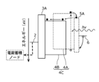
- FIG. 3 is a diagram showing an example of a circuit configuration of an imaging device 100 in which a photoelectric conversion section 10A using the photoelectric conversion element 10 shown in FIG. 1 is mounted.
- FIG. 4 is a schematic cross-sectional view showing an example of the device structure of the pixel 24 in the imaging device 100 according to the present embodiment.
- the imaging device 100 includes a semiconductor substrate 40, a charge detection circuit 35 provided on the semiconductor substrate 40, and a photoelectric conversion unit provided on the semiconductor substrate 40. 10A, and a plurality of pixels 24 each including a charge storage node 34 electrically connected to the charge detection circuit 35 and the photoelectric conversion unit 10A. It includes element 10 . That is, each of the plurality of pixels 24 includes an upper electrode 6, a lower electrode 2, a photoelectric conversion layer 4, a charge injection layer 5, a charge blocking layer 3, and a charge storage node .
- the charge storage node 34 is an example of a charge storage region.
- the upper electrode 6, the charge injection layer 5, the photoelectric conversion layer 4, the charge blocking layer 3, and the lower electrode 2 are arranged in this order from the light incident side of the photoelectric conversion section 10A.
- the charge injection layer 5 is located on the light incident side of the photoelectric conversion layer 4 .
- Light transmitted through the upper electrode 6 and the charge injection layer 5 enters the photoelectric conversion layer 4 . Therefore, excitons are likely to be generated on the charge injection layer 5 side of the photoelectric conversion layer 4 .
- the light incident side of the photoelectric conversion section 10A is the side opposite to the semiconductor substrate 40 side of the photoelectric conversion section 10A.
- the charge accumulation node 34 accumulates the charge obtained by the photoelectric conversion unit 10A, and the charge detection circuit 35 detects the charge accumulated in the charge accumulation node 34.
- the charge detection circuit 35 provided on the semiconductor substrate 40 may be provided on the semiconductor substrate 40 or may be provided in the semiconductor substrate 40 .
- the imaging device 100 includes a plurality of pixels 24 and peripheral circuits.
- the imaging device 100 is, for example, an organic image sensor realized by a one-chip integrated circuit, and has a pixel array PA including a plurality of pixels 24 arranged two-dimensionally.
- a plurality of pixels 24 are arranged two-dimensionally on a semiconductor substrate 40, that is, in row and column directions to form a photosensitive region, which is a pixel region.
- FIG. 3 shows an example in which the pixels 24 are arranged in a matrix of 2 rows and 2 columns.
- FIG. 3 omits illustration of a circuit (for example, a pixel electrode control circuit) for individually setting the sensitivity of the pixels 24 .
- the imaging device 100 may be a line sensor.
- the plurality of pixels 24 may be arranged one-dimensionally.
- the row direction and column direction refer to directions in which rows and columns extend, respectively. That is, in FIG. 3, the vertical direction on the paper surface is the column direction, and the horizontal direction is the row direction.
- each pixel 24 includes a photoelectric conversion section 10A and a charge storage node 34 electrically connected to a charge detection circuit 35.
- FIG. The charge detection circuit 35 includes an amplification transistor 21 , a reset transistor 22 and an address transistor 23 .
- the photoelectric conversion unit 10A includes a lower electrode 2 provided as a pixel electrode and an upper electrode 6 provided as a counter electrode facing the pixel electrode.
- the photoelectric conversion unit 10A includes the photoelectric conversion element 10 described above.
- a voltage for applying a predetermined bias voltage is supplied to the upper electrode 6 via a counter electrode signal line 26 .
- the lower electrode 2 is connected to the gate electrode 21G of the amplification transistor 21, and the signal charge collected by the lower electrode 2 is accumulated in the charge accumulation node 34 located between the lower electrode 2 and the gate electrode 21G of the amplification transistor 21. be done.
- the signal charges are holes. That is, the charge storage node 34 is electrically connected to the lower electrode 2 and stores holes among the excitons generated in the photoelectric conversion layer 4 .
- the signal charge accumulated in the charge accumulation node 34 is applied to the gate electrode 21G of the amplification transistor 21 as a voltage corresponding to the amount of signal charge.
- the amplification transistor 21 amplifies this voltage and is selectively read by the address transistor 23 as a signal voltage.
- the reset transistor 22 has its source/drain electrodes connected to the lower electrode 2 and resets the signal charge accumulated in the charge accumulation node 34 . In other words, the reset transistor 22 resets the potentials of the gate electrode 21 ⁇ /b>G and the lower electrode 2 of the amplification transistor 21 .
- the imaging device 100 has power supply wiring 31, vertical signal line 27, address signal line 36, and reset signal line 37, and these lines are are connected to each pixel 24 respectively.
- the power supply wiring 31 is connected to the source/drain electrodes of the amplification transistor 21
- the vertical signal line 27 is connected to the source/drain electrodes of the address transistor 23 .
- the address signal line 36 is connected to the gate electrode 23G of the address transistor 23.
- FIG. Also, the reset signal line 37 is connected to the gate electrode 22G of the reset transistor 22 .
- the peripheral circuits include a voltage supply circuit 19, a vertical scanning circuit 25, a horizontal signal readout circuit 20, a plurality of column signal processing circuits 29, a plurality of load circuits 28, and a plurality of differential amplifiers 32.
- the voltage supply circuit 19 is electrically connected to the upper electrode 6 via the counter electrode signal line 26 .
- the voltage supply circuit 19 provides a potential difference between the upper electrode 6 and the lower electrode 2 by supplying voltage to the upper electrode 6 .
- the voltage supply circuit 19 supplies the upper electrode 6 with a voltage that makes the potential of the upper electrode 6 higher than the potential of the lower electrode 2 . In this case, the upper electrode 6 becomes an anode and the lower electrode 2 becomes a cathode.
- the voltage supply circuit 19 supplies the upper electrode 6 with a voltage that makes the potential of the upper electrode 6 lower than the potential of the lower electrode 2 . In this case, the upper electrode 6 becomes a cathode and the lower electrode 2 becomes an anode.
- the vertical scanning circuit 25 is connected to an address signal line 36 and a reset signal line 37, selects a plurality of pixels 24 arranged in each row in units of rows, and reads signal voltages and resets the potential of the lower electrode 2. conduct.
- a power supply line 31 that is a source follower power supply supplies a predetermined power supply voltage to each pixel 24 .
- the horizontal signal readout circuit 20 is electrically connected to a plurality of column signal processing circuits 29 .
- the column signal processing circuit 29 is electrically connected to the pixels 24 arranged in each column via vertical signal lines 27 corresponding to each column.
- a load circuit 28 is electrically connected to each vertical signal line 27 .
- the load circuit 28 and the amplification transistor 21 form a source follower circuit.
- a plurality of differential amplifiers 32 are provided corresponding to each column.
- An inverting input terminal of the differential amplifier 32 is connected to the corresponding vertical signal line 27 .
- An output terminal of the differential amplifier 32 is connected to the pixels 24 via feedback lines 33 corresponding to each column.
- the vertical scanning circuit 25 applies a row selection signal for controlling ON/OFF of the address transistor 23 to the gate electrode 23G of the address transistor 23 through the address signal line 36 .
- the rows to be read are scanned and selected.
- a signal voltage is read out to the vertical signal line 27 from the pixels 24 in the selected row.
- the vertical scanning circuit 25 applies a reset signal for controlling ON/OFF of the reset transistor 22 to the gate electrode 22G of the reset transistor 22 via the reset signal line 37 . This selects a row of pixels 24 to be reset.
- the vertical signal line 27 transmits the signal voltage read from the pixel 24 selected by the vertical scanning circuit 25 to the column signal processing circuit 29 .
- the column signal processing circuit 29 performs noise suppression signal processing typified by correlated double sampling and analog-digital conversion (AD conversion).
- the horizontal signal readout circuit 20 sequentially reads signals from the plurality of column signal processing circuits 29 to a horizontal common signal line (not shown).
- the differential amplifier 32 is connected to the drain electrode of the reset transistor 22 via the feedback line 33. Therefore, differential amplifier 32 receives the output value of address transistor 23 at its inverting input terminal.
- the differential amplifier 32 performs a feedback operation so that the gate potential of the amplification transistor 21 becomes a predetermined feedback voltage. At this time, the output voltage value of the differential amplifier 32 is 0V or a positive voltage near 0V. Feedback voltage means the output voltage of the differential amplifier 32 .
- the pixel 24 includes a semiconductor substrate 40, a charge detection circuit 35, a photoelectric conversion section 10A and a charge storage node 34 (see FIG. 3).
- the semiconductor substrate 40 may be an insulating substrate or the like having a semiconductor layer provided on the surface on which the photosensitive region is formed, such as a p-type silicon substrate.
- the semiconductor substrate 40 has impurity regions 21D, 21S, 22D, 22S and 23S and an isolation region 41 for electrical isolation between the pixels 24 .
- Impurity regions 21D, 21S, 22D, 22S and 23S are, for example, n-type regions.
- the element isolation region 41 is provided between the impurity region 21D and the impurity region 22D. This suppresses leakage of signal charges accumulated in the charge accumulation node 34 .
- the element isolation region 41 is formed, for example, by implanting acceptor ions under predetermined implantation conditions.
- the impurity regions 21D, 21S, 22D, 22S and 23S are diffusion regions formed in the semiconductor substrate 40, for example.
- amplification transistor 21 includes impurity regions 21S and 21D, and gate electrode 21G.
- Impurity region 21S and impurity region 21D function as, for example, a source region and a drain region of amplifying transistor 21, respectively.
- a channel region of amplification transistor 21 is formed between impurity region 21S and impurity region 21D.
- the address transistor 23 includes an impurity region 23S, an impurity region 21S, and a gate electrode 23G connected to the address signal line 36.
- amplification transistor 21 and address transistor 23 are electrically connected to each other by sharing impurity region 21S.
- the impurity region 23S functions as a source region of the address transistor 23, for example.
- Impurity region 23S has a connection with vertical signal line 27 shown in FIG.
- the reset transistor 22 includes impurity regions 22D and 22S and a gate electrode 22G connected to the reset signal line 37.
- the impurity region 22S functions as a source region of the reset transistor 22, for example.
- Impurity region 22S has a connection with feedback line 33 shown in FIG.
- An interlayer insulating layer 50 is laminated on the semiconductor substrate 40 so as to cover the amplification transistor 21 , the address transistor 23 and the reset transistor 22 .
- a wiring layer (not shown) may be arranged in the interlayer insulating layer 50 .
- the wiring layer is made of metal such as copper, and may include wiring such as the vertical signal lines 27 described above.
- the number of insulating layers in interlayer insulating layer 50 and the number of wiring layers arranged in interlayer insulating layer 50 can be set arbitrarily.
- the impurity region 22D of the reset transistor 22 is electrically connected to the gate electrode 21G of the amplification transistor 21.
- contact plugs 51, 53 and 54, wiring 52, gate electrode 21G of amplifying transistor 21, and impurity region 22D of reset transistor 22 constitute at least part of charge storage node 34. .
- the charge detection circuit 35 detects signal charges collected by the lower electrode 2 and outputs a signal voltage.
- the charge detection circuit 35 includes an amplification transistor 21 , a reset transistor 22 and an address transistor 23 and is formed on a semiconductor substrate 40 .
- the amplification transistor 21 is formed in the semiconductor substrate 40 and includes an impurity region 21D and an impurity region 21S functioning as a drain electrode and a source electrode, respectively, a gate insulating layer 21X formed on the semiconductor substrate 40, and a gate insulating layer 21X formed on the gate insulating layer 21X. and a gate electrode 21G formed on the .
- the reset transistor 22 is formed in the semiconductor substrate 40 and includes an impurity region 22D and an impurity region 22S functioning as a drain electrode and a source electrode, respectively, a gate insulating layer 22X formed on the semiconductor substrate 40, and a gate insulating layer 22X on the gate insulating layer 22X. and a gate electrode 22G formed on the .
- Address transistor 23 is formed in semiconductor substrate 40 and formed on impurity regions 21S and 23S functioning as a drain electrode and a source electrode, respectively, gate insulating layer 23X formed on semiconductor substrate 40, and gate insulating layer 23X. and a gate electrode 23G.
- Impurity region 21S is connected in series with amplifying transistor 21 and address transistor 23 .
- the photoelectric conversion section 10A described above is arranged on the interlayer insulating layer 50 .
- the plurality of pixels 24 forming the pixel array PA are formed on the semiconductor substrate 40 .
- a plurality of pixels 24 two-dimensionally arranged on the semiconductor substrate 40 form a photosensitive region.
- the distance (that is, pixel pitch) between two connected pixels 24 may be, for example, about 2 ⁇ m.
- the photoelectric conversion unit 10A has the structure of the photoelectric conversion element 10 described above.
- a color filter 60 is formed above the photoelectric conversion unit 10A, and a microlens 61 is formed thereabove.
- the color filter 60 is formed as an on-chip color filter by patterning, for example.
- a photosensitive resin in which dyes or pigments are dispersed is used as the material of the color filter 60 .
- the microlens 61 is formed, for example, as an on-chip microlens.
- An ultraviolet sensitive material or the like is used as the material of the microlenses 61 .
- the imaging device 100 can use a general semiconductor manufacturing process.
- a silicon substrate is used as the semiconductor substrate 40, it can be manufactured by using various silicon semiconductor processes.
- the imaging device 100 may operate in a rolling shutter method in which a plurality of pixels 24 are sequentially exposed for each pixel row and read out signals, or may operate in a global shutter method in which the exposure periods of the plurality of pixels 24 are unified. good too.
- the voltage supply circuit 19 continues to supply the upper electrode 6 with the first voltage that causes sensitivity in the photoelectric conversion unit 10A, for example, during imaging. Readout operations of signal charges are sequentially performed. Further, when operating in the global shutter system, the voltage supply circuit 19 supplies, for example, the first voltage to the upper electrode 6 during the exposure period, and the first voltage so as not to cause sensitivity in the photoelectric conversion section 10A during the non-exposure period. 2 voltages are applied to the upper electrode 6 . During this non-exposure period, signal charges are read out sequentially for each pixel row. Note that the readout operation of the imaging device 100 is not limited to such an operation, and a known readout operation of an imaging device can be applied.
- FIG. 5 is an exemplary energy band diagram in another photoelectric conversion element according to this embodiment.
- the energy bands of each layer are indicated by rectangles.
- black circles indicate electrons and white circles indicate holes, and part of the movement of electrons and holes is schematically shown.
- the energy band of the donor semiconductor material 4A and the energy band of the acceptor semiconductor material 4B are shown shifted in the horizontal direction. It does not mean that the donor semiconductor material 4A and the acceptor semiconductor material 4B are separately distributed in the thickness direction of the layer 4C.
- the energy bands of the donor semiconductor material 4A and the charge injection layer 5A are indicated by broken-line rectangles, but this is also for the sake of visibility and is not intended to be distinguished from the solid-line rectangles.
- FIG. 1 The energy bands of a photoelectric conversion device comprising layer 4C, charge blocking layer 3A and charge injection layer 5A are shown.
- the ionization potential of the charge blocking layer 3A is, for example, higher than the ionization potential of the donor semiconductor material 4A of the photoelectric conversion layer 4C.
- the charge blocking layer 3A suppresses injection of charges (specifically, holes) from the lower electrode 2 to the photoelectric conversion layer 4C. As a result, noise signals that adversely affect the SN ratio can be reduced.
- the electron affinity of the charge injection layer 5A is greater than or equal to the electron affinity of the donor semiconductor material 4A.
- the electron affinity of the charge injection layer 5A may be greater than the electron affinity of the donor semiconductor material 4A.
- the ionization potential of the charge injection layer 5A is higher than the ionization potential of the donor semiconductor material 4A.
- the ionization potential of the charge injection layer 5A may be higher than the ionization potential of the donor semiconductor material 4A.
- the charge injection layer 5A having such an energy band can suppress the injection of charges (specifically, electrons) from the upper electrode 6 to the photoelectric conversion layer 4C, thereby suppressing noise signals that adversely affect the SN ratio. can be reduced.
- the value obtained by subtracting the electron affinity of the charge injection layer 5A from the electron affinity of the acceptor semiconductor material 4B is, for example, greater than the value obtained by subtracting the electron affinity of the acceptor semiconductor material 4B from the electron affinity of the charge blocking layer 3A.
- the smaller the value obtained by subtracting the electron affinity of the charge injection layer 5A from the electron affinity of the acceptor semiconductor material 4B the greater the barrier for electrons to hop and move from the charge injection layer 5A to the acceptor semiconductor material 4B.
- the smaller the value obtained by subtracting the electron affinity of the acceptor semiconductor material 4B from the electron affinity of the charge blocking layer 3A the greater the barrier for electrons to hop and move from the acceptor semiconductor material 4B to the charge blocking layer 3A.
- the barrier when electrons hop from the charge injection layer 5A to the acceptor semiconductor material 4B is the barrier when electrons hop from the acceptor semiconductor material 4B to the charge blocking layer 3A. smaller than the barrier. Therefore, the movement of the separated electrons from the charge injection layer 5 to the acceptor semiconductor material 4B does not become rate-limiting for electron collection by the lower electrode 2, so electrons are efficiently collected.
- the electron affinity of the charge injection layer 5A is, for example, lower than the electron affinity of the acceptor semiconductor material 4B. This makes it easier for the separated electrons to move from the charge injection layer 5A to the acceptor semiconductor material 4B.
- the ratio of the donor semiconductor material 4A in the photoelectric conversion layer 4C is, for example, 70% or more.
- the acceptor semiconductor material 4B is, for example, 50% or less of the donor semiconductor material 4A.
- the contact interface between the donor semiconductor material 4A and the charge injection layer 5A is increased, so that the effect of improving the sensitivity can be obtained more remarkably.
- the ratio of materials is, for example, a volume ratio, it may be a weight ratio.
- the photoelectric conversion elements provided in the imaging apparatus according to the present disclosure will be specifically described below in Examples, but the present disclosure is not limited to the following Examples. Specifically, a photoelectric conversion element provided in an imaging device according to an embodiment of the present disclosure and a photoelectric conversion element for characteristic comparison were manufactured, and spectral sensitivities were measured.
- Example 1 A substrate on which TiN was deposited was used as a support substrate. TiN having a work function of 4.7 eV is used as the lower electrode, and 9,9′-[1,1′-Biphenyl]-4,4′-diylbis[3,6-bis(1,1-dimethyl ethyl)]-9H-carbazole was deposited by a vacuum deposition method to form a charge blocking layer. Next, subphthalocyanine, which is a donor semiconductor material, and fullerene C60, which is an acceptor semiconductor material, are co-deposited on the charge blocking layer by a vacuum deposition method as materials for the photoelectric conversion layer, thereby forming a photoelectric conversion layer. formed.
- subphthalocyanine which is a donor semiconductor material
- fullerene C60 which is an acceptor semiconductor material
- the volume ratio of the donor semiconductor material and the acceptor semiconductor material was 1:3. Moreover, the film thickness of the photoelectric conversion layer obtained at this time was about 500 nm.
- the subphthalocyanine a subphthalocyanine having boron (B) as a central metal and chloride ions coordinated to B as a ligand was used.
- a charge injection layer was formed by vapor-depositing subphthalocyanine as a material for the charge injection layer to a thickness of 5 nm through a metal shadow mask by a vacuum vapor deposition method.
- Example 2 9,9′-[1,1′-Biphenyl]-4,4′-diylbis[3,6-bis(1,1-dimethyl ethyl)]-9H-carbazole instead of subphthalocyanine as a material for the charge injection layer
- a photoelectric conversion element was obtained by performing the same steps as in Example 1, except that .
- Example 1 A photoelectric conversion element was obtained by performing the same steps as in Example 1, except that the upper electrode was formed directly on the photoelectric conversion layer without forming the charge injection layer.
- samples were prepared by forming films of the respective materials used in Examples 1, 2, and Comparative Example 1 on glass substrates on which ITO was formed.
- an atmospheric photoelectron spectrometer AC-3, manufactured by Riken Keiki Co., Ltd. was used to measure the number of photoelectrons when the energy of ultraviolet irradiation was changed, and the energy position at which photoelectrons began to be detected was defined as the ionization potential.
- Table 1 shows the ionization potential and electron affinity of each material used in Examples 1, 2, and Comparative Example 1.
- the ionization potential of the charge injection layer was equal to or lower than the ionization potential of the acceptor semiconductor material, and the electron affinity of the charge injection layer It is less than the electron affinity of the semiconductor material. Further, in the photoelectric conversion elements of Examples 1 and 2, the value obtained by subtracting the ionization potential of the charge injection layer from the ionization potential of the donor semiconductor material is 0 or less, and the ionization potential of the charge blocking layer is less than the ionization potential of the donor semiconductor material. less than the value minus the ionization potential of the material.
- the external quantum efficiency was measured as an index of spectral sensitivity.
- a photoelectric conversion element is introduced into a measurement jig that can be sealed in a glove box under a nitrogen atmosphere, and a spectral sensitivity measurement device (manufactured by Spectroscopy Instruments) is used to measure the The external quantum efficiency of the photoelectric conversion device was measured.
- a voltage was applied so that the potential of the upper electrode was higher than the potential of the lower electrode. That is, the external quantum efficiency of the photoelectric conversion device was measured under the condition that electrons move to the upper electrode and holes move to the lower electrode.
- the relative external quantum efficiency which is the ratio of the external quantum efficiency to that of Comparative Example 1, was calculated using the following formula.
- Relative external quantum efficiency (%) external quantum efficiency of photoelectric conversion element/external quantum efficiency of Comparative Example 1 ⁇ 100
- Table 2 shows the measurement results of the relative external quantum efficiencies of the photoelectric conversion devices in Example 1, Example 2, and Comparative Example 1.
- Examples 1 and 2 have higher relative external quantum efficiencies than Comparative Example 1. This is because, in the photoelectric conversion elements of Examples 1 and 2, the charge injection layer and the acceptor semiconductor material were separated because the ionization potential of the charge injection layer was lower than the ionization potential of the acceptor semiconductor material. It is considered that the holes contribute to the sensitivity, and the sensitivity is higher than that of Comparative Example 1 in which the charge injection layer is not formed.
- the imaging apparatus has been described above based on the embodiments and examples, the present disclosure is not limited to these embodiments and examples. As long as it does not depart from the gist of the present disclosure, various modifications that a person skilled in the art can think of are applied to the embodiments and examples, and other forms constructed by combining some components of the embodiments and examples are also within the scope of this disclosure.
- the imaging device can be applied to various camera systems and sensor systems such as medical cameras, surveillance cameras, in-vehicle cameras, ranging cameras, microscope cameras, drone cameras, and robot cameras.
- Reference Signs List 1 support substrate 2 lower electrodes 3, 3A charge blocking layers 4, 4C photoelectric conversion layer 4A donor semiconductor material 4B acceptor semiconductor materials 5, 5A charge injection layer 6 upper electrode 10 photoelectric conversion element 10A photoelectric conversion section 19 voltage supply circuit 20 horizontal signal readout circuit 21 amplification transistor 22 reset transistor 23 address transistors 21D, 21S, 22D, 22S, 23S impurity regions 21G, 22G, 23G gate electrodes 21X, 22X, 23X gate insulating layer 24 pixel 25 vertical scanning circuit 26 counter electrode signal line 27 vertical signal line 28 load circuit 29 column signal processing circuit 31 power supply line 32 differential amplifier 33 feedback line 34 charge storage node 35 charge detection circuit 36 address signal line 37 reset signal line 40 semiconductor substrate 41 element isolation region 50 interlayer insulating layer 51 , 53, 54 contact plug 52 wiring 60 color filter 61 microlens 100 imaging device
Landscapes
- Physics & Mathematics (AREA)
- Electromagnetism (AREA)
- Solid State Image Pick-Up Elements (AREA)
- Light Receiving Elements (AREA)
Priority Applications (3)
| Application Number | Priority Date | Filing Date | Title |
|---|---|---|---|
| CN202280068405.1A CN118104414A (zh) | 2021-10-26 | 2022-09-27 | 摄像装置 |
| JP2023556218A JPWO2023074230A1 (https=) | 2021-10-26 | 2022-09-27 | |
| US18/626,366 US20240276744A1 (en) | 2021-10-26 | 2024-04-04 | Imaging apparatus |
Applications Claiming Priority (2)
| Application Number | Priority Date | Filing Date | Title |
|---|---|---|---|
| JP2021174266 | 2021-10-26 | ||
| JP2021-174266 | 2021-10-26 |
Related Child Applications (1)
| Application Number | Title | Priority Date | Filing Date |
|---|---|---|---|
| US18/626,366 Continuation US20240276744A1 (en) | 2021-10-26 | 2024-04-04 | Imaging apparatus |
Publications (1)
| Publication Number | Publication Date |
|---|---|
| WO2023074230A1 true WO2023074230A1 (ja) | 2023-05-04 |
Family
ID=86159769
Family Applications (1)
| Application Number | Title | Priority Date | Filing Date |
|---|---|---|---|
| PCT/JP2022/035984 Ceased WO2023074230A1 (ja) | 2021-10-26 | 2022-09-27 | 撮像装置 |
Country Status (4)
| Country | Link |
|---|---|
| US (1) | US20240276744A1 (https=) |
| JP (1) | JPWO2023074230A1 (https=) |
| CN (1) | CN118104414A (https=) |
| WO (1) | WO2023074230A1 (https=) |
Citations (9)
| Publication number | Priority date | Publication date | Assignee | Title |
|---|---|---|---|---|
| US20050110007A1 (en) * | 2003-11-26 | 2005-05-26 | Forrest Stephen R. | Multilayer organic photodetectors with improved performance |
| JP2009099866A (ja) * | 2007-10-18 | 2009-05-07 | Fujifilm Corp | 光電変換素子及び固体撮像素子 |
| JP2010263175A (ja) * | 2009-05-05 | 2010-11-18 | Jiaotong Univ | 有機感光性の光電装置 |
| JP2015233117A (ja) * | 2014-05-13 | 2015-12-24 | ソニー株式会社 | 光電変換膜、固体撮像素子、および電子機器 |
| JP2016225456A (ja) * | 2015-05-29 | 2016-12-28 | パナソニックIpマネジメント株式会社 | 撮像装置および光電変換膜の製造方法 |
| WO2017077790A1 (ja) * | 2015-11-02 | 2017-05-11 | ソニー株式会社 | 光電変換素子および固体撮像装置 |
| JP2018085427A (ja) * | 2016-11-22 | 2018-05-31 | ソニー株式会社 | 撮像素子、積層型撮像素子、撮像装置及び電子装置 |
| WO2020008186A1 (en) * | 2018-07-06 | 2020-01-09 | Sumitomo Chemical Co., Ltd | Organic photodetector |
| WO2020162095A1 (ja) * | 2019-02-08 | 2020-08-13 | パナソニックIpマネジメント株式会社 | 光電変換素子および撮像装置 |
-
2022
- 2022-09-27 JP JP2023556218A patent/JPWO2023074230A1/ja active Pending
- 2022-09-27 WO PCT/JP2022/035984 patent/WO2023074230A1/ja not_active Ceased
- 2022-09-27 CN CN202280068405.1A patent/CN118104414A/zh active Pending
-
2024
- 2024-04-04 US US18/626,366 patent/US20240276744A1/en active Pending
Patent Citations (9)
| Publication number | Priority date | Publication date | Assignee | Title |
|---|---|---|---|---|
| US20050110007A1 (en) * | 2003-11-26 | 2005-05-26 | Forrest Stephen R. | Multilayer organic photodetectors with improved performance |
| JP2009099866A (ja) * | 2007-10-18 | 2009-05-07 | Fujifilm Corp | 光電変換素子及び固体撮像素子 |
| JP2010263175A (ja) * | 2009-05-05 | 2010-11-18 | Jiaotong Univ | 有機感光性の光電装置 |
| JP2015233117A (ja) * | 2014-05-13 | 2015-12-24 | ソニー株式会社 | 光電変換膜、固体撮像素子、および電子機器 |
| JP2016225456A (ja) * | 2015-05-29 | 2016-12-28 | パナソニックIpマネジメント株式会社 | 撮像装置および光電変換膜の製造方法 |
| WO2017077790A1 (ja) * | 2015-11-02 | 2017-05-11 | ソニー株式会社 | 光電変換素子および固体撮像装置 |
| JP2018085427A (ja) * | 2016-11-22 | 2018-05-31 | ソニー株式会社 | 撮像素子、積層型撮像素子、撮像装置及び電子装置 |
| WO2020008186A1 (en) * | 2018-07-06 | 2020-01-09 | Sumitomo Chemical Co., Ltd | Organic photodetector |
| WO2020162095A1 (ja) * | 2019-02-08 | 2020-08-13 | パナソニックIpマネジメント株式会社 | 光電変換素子および撮像装置 |
Also Published As
| Publication number | Publication date |
|---|---|
| CN118104414A (zh) | 2024-05-28 |
| JPWO2023074230A1 (https=) | 2023-05-04 |
| US20240276744A1 (en) | 2024-08-15 |
Similar Documents
| Publication | Publication Date | Title |
|---|---|---|
| JP7535701B2 (ja) | 撮像装置 | |
| US12433087B2 (en) | Imaging device | |
| US12289552B2 (en) | Imaging device and driving method | |
| US20230045956A1 (en) | Photoelectric conversion element and imaging apparatus | |
| US20210273019A1 (en) | Imaging device, method for manufacturing imaging device, and imaging apparatus | |
| US11723224B2 (en) | Imaging apparatus | |
| CN118985183A (zh) | 光电转换元件及摄像装置 | |
| US20240276744A1 (en) | Imaging apparatus | |
| US20260033121A1 (en) | Imaging device | |
| US20260025600A1 (en) | Imaging device | |
| US12082427B2 (en) | Imaging device, method for manufacturing imaging device, and imaging apparatus | |
| US20250393385A1 (en) | Photoelectric conversion element and imaging device | |
| US20260032355A1 (en) | Imaging device | |
| WO2024214448A1 (ja) | 光電変換素子および撮像装置 | |
| WO2024150622A1 (ja) | 光電変換素子および撮像装置 | |
| WO2025173447A1 (ja) | 光電変換素子および撮像装置 | |
| WO2025173448A1 (ja) | 光電変換素子、撮像装置および光電変換素子の製造方法 |
Legal Events
| Date | Code | Title | Description |
|---|---|---|---|
| 121 | Ep: the epo has been informed by wipo that ep was designated in this application |
Ref document number: 22886562 Country of ref document: EP Kind code of ref document: A1 |
|
| WWE | Wipo information: entry into national phase |
Ref document number: 2023556218 Country of ref document: JP |
|
| WWE | Wipo information: entry into national phase |
Ref document number: 202280068405.1 Country of ref document: CN |
|
| NENP | Non-entry into the national phase |
Ref country code: DE |
|
| 122 | Ep: pct application non-entry in european phase |
Ref document number: 22886562 Country of ref document: EP Kind code of ref document: A1 |