WO2023068137A1 - デバイストレイ - Google Patents
デバイストレイ Download PDFInfo
- Publication number
- WO2023068137A1 WO2023068137A1 PCT/JP2022/038042 JP2022038042W WO2023068137A1 WO 2023068137 A1 WO2023068137 A1 WO 2023068137A1 JP 2022038042 W JP2022038042 W JP 2022038042W WO 2023068137 A1 WO2023068137 A1 WO 2023068137A1
- Authority
- WO
- WIPO (PCT)
- Prior art keywords
- device tray
- tray according
- image
- filament
- closing
- Prior art date
- Legal status (The legal status is an assumption and is not a legal conclusion. Google has not performed a legal analysis and makes no representation as to the accuracy of the status listed.)
- Ceased
Links
Images


Classifications
-
- H—ELECTRICITY
- H01—ELECTRIC ELEMENTS
- H01G—CAPACITORS; CAPACITORS, RECTIFIERS, DETECTORS, SWITCHING DEVICES, LIGHT-SENSITIVE OR TEMPERATURE-SENSITIVE DEVICES OF THE ELECTROLYTIC TYPE
- H01G13/00—Apparatus specially adapted for manufacturing capacitors; Processes specially adapted for manufacturing capacitors not provided for in groups H01G4/00 - H01G11/00
Definitions
- the present invention relates to a device tray, and more particularly to a device tray for storing devices and providing them for post-processing steps such as transportation and heating.
- Patent Literature 1 proposes identifying the type of device tray in a jig for chip-shaped electronic components by coloring part of the surface of the device tray with a different color from the rest of the device tray. ing.
- an object of the present invention is to provide a device tray that solves the above-described problems of marking due to coloring or the like by making the marking on the device tray easy to recognize.
- At least one of a filament portion composed of a plurality of intersecting filament members, a plurality of device storage portions formed by stacked filament portions, and a device storage portion is provided. and a closing closure.
- a device tray according to an aspect of the present invention is characterized in that the closing part is integrated with the filament part.
- the device storage section has a cubic or rectangular parallelepiped shape, and at least four corners forming the cube or rectangular parallelepiped of the device storage section are closed by the closing section.
- a device tray according to an aspect of the present invention is characterized in that the closing part completely closes at least one device storage part.
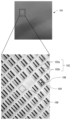
- FIG. 1 is an example of a device tray viewed from above and a partially enlarged view thereof according to an embodiment of the present invention
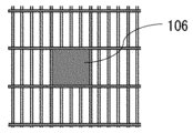
- FIG. FIG. 2A is a schematic diagram showing examples of various aspects of the closure.
- FIG. 2B is a schematic diagram showing examples of various aspects of the closure.
- FIG. 2C is a schematic diagram showing examples of various aspects of the closure.
- FIG. 2D is a schematic diagram illustrating examples of various aspects of the occlusion.
- FIG. 2E is a schematic diagram showing examples of various aspects of the occlusion.
- FIG. 2F is a schematic diagram showing examples of various aspects of the occlusion.
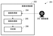
- FIG. 3 is a diagram showing an overview of a system 201 for determining the presence or absence of blockage 106 or the type of blockage 106 .
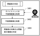
- FIG. 4 is a flow chart showing the flow of determination as to the presence or absence of a blockage or the type of blockage.
- FIG. 1 is an example of a device tray 101 viewed from above and an enlarged view of a part thereof as one embodiment of the present invention.
- a device tray 101 according to the present invention includes a filament portion 102 composed of a plurality of intersecting filament members (102a, 102b), a plurality of device storage portions 104 formed by the stacked filament portions 102, and a device storage portion. and a closure 106 that closes at least one of 104 .
- the filamentary portion 102 of the device tray 101 is composed of a plurality of intersecting filamentous members (102a, 102b).
- the first filament member 102a and the second filament member 102b preferably intersect each other at right angles as in the example of FIG. .
- the plurality of first wire members 102a are preferably parallel to each other.
- the plurality of second filament members 102b are preferably parallel to each other.
- the filament portion 102 is formed in a mesh shape by a first filament member 102a and a second filament member 102b.
- the filaments 102 are stacked vertically to form multiple layers.
- a space surrounded by the stacked linear portions 102 becomes a device storage portion 104 for storing a device.
- a plurality of device storage sections 104 are formed by the stacked filament sections 102 .
- the device housing portion 104 preferably has a cubic or cuboid shape.
- the device housing portion 104 has at least four corners forming a cube or a rectangular parallelepiped of the device housing portion 104 closed by a closing portion 106 .
- the closing part 106 is preferably integrated with the filament part 102 .
- the material used to block the blocking portion 106 is preferably the same material as the material forming the filamentous portion 102. By blocking the blocking portion 106 with the same material as the filamentous portion 102, the blocking portion 106 may be integrated with the filament portion 102 . Also, the material for closing the closing portion 106 may be a material different from the material forming the filament portion 102 . The closing portion 106 may be adhered to the filar portion 102 .
- FIG. Figures 2A-2F are schematic diagrams illustrating examples of various aspects of closure 106.
- FIG. Figures 2A-2F show examples of closures 106 according to the first to sixth aspects, respectively.
- the closing portion 106 completely closes at least one device storage portion 104 .
- the number of closed device storage units 104 is arbitrary. In the example of FIG. 2A, one device storage section 104 is closed, but the present invention is not limited to this, and two device storage sections 104 may be closed as in the example of FIG. Also, as in the example of FIG. 1, two adjacent device storage sections 104 may be closed, but a plurality of closed device storage sections 104 may be provided at positions separated from each other.
- two or more device housings 104 may be closed such that the closures 106 are aligned.
- two or more blocking portions 106 arranged in a straight line may be arranged to form a "two" shape or an "L” shape.
- three blocking portions 106 that are two or more arranged in a straight line may be arranged to form a “U” shape or an “H” shape.
- two or more device storage units 104 are closed, one or more straight lines formed by two or more closing units 106 are provided, and arbitrary character shapes such as alphabets, hiragana, and katakana are formed. This makes it possible to emphasize the performance of image recognition.
- the blocking portion 106 may have an opening 108 that does not block the device storage portion 104.
- the depth of the opening 108 may be any depth within the range where the opening 108 does not penetrate the device housing portion 104 . Having the opening 108 that does not block the blocking part 106 makes it possible to emphasize the performance of image recognition using the edge of the opening.
- the opening 108 may be circular, linear, or polygonal in plan view.
- the circle may be a perfect circle or an ellipse of any shape.
- a line can be any straight line or curve.
- Polygons may be triangles, quadrilaterals, rectangles, squares, or any rectangular shape. By providing such a specific shape, it becomes easy to identify each individual by using the opening 108 as a recognition mark.
- the opening 108 may have a shape representing characters or symbols in plan view.
- the characters may be any characters, such as alphabets, hiragana, katakana, kanji, or characters used in other languages.
- any symbols such as pictograms, marks, barcodes, and QR codes (registered trademark) may be used.
- arbitrarily created original symbols may be used. .
- part of the upper surface of the closing portion 106 may be printed or stamped to represent letters, symbols, figures or patterns.
- the closure 106 has an opening 108 that does not block the device housing 104, whereas in the example of FIG. 2F, the closure 106 does not have the opening 108.
- a portion of the upper surface of the closure portion 106 is printed with letters, symbols, graphics or patterns, or a portion of the upper surface of the closure portion 106 is engraved with letters, symbols, graphics or patterns.
- the characters, symbols, figures or patterns are slightly recessed, recessed or grooved, but unlike the openings 108, the bottom layer of the filament 102 reaches a depth that allows it to be visually recognized. do not.
- the closing part 106 described with reference to FIGS. 2A to 2F may be provided in the central part of the device tray 101.
- FIG. When the closing portion 106 is provided in the central portion of the device tray 101, compared with the case where the closing portion 106 is provided only in the end portion of the device tray 101, there is an effect of improving the alignment accuracy with respect to the central portion of the device tray 101.
- FIG. For example, when the device tray 101 is made of ceramic, when the ceramic is sintered, the dimensions of one side of the device tray 101 (X direction) and the direction perpendicular thereto (Y direction) shrink. Therefore, in the manufacturing process of the device tray 101, when the shrinkage rate is large, the pitch may change between the vicinity of the center of the device tray 101 and the edge. By providing the blocking part 106 in the central part of the device tray 101, even in such a case, there is an effect that the recognition can be easily corrected.
- the closing portion 106 is formed by pouring the material of the closing portion 106 into the device housing portion 104 formed by the laminated filament portions 102 .
- the material of the closing part 106 may be clay-like, liquid-like, or gel-like.
- the closure 106 can be formed by pre-solidifying the material of the closure 106 to form a solid that conforms to the shape and size of the device housing 104 and inserting the formed solid into the device housing 104 . may be formed.
- the filament portion 102 and the solid may be fixed with an adhesive substance.
- the method of forming the closing portion 106 is not limited to these, and may be formed by any other method.
- FIGS. 2B to 2E if the closure 106 has an opening 108, the closure 106 is mechanically cut, laser processed, sandblasted, wet blasted, etched, or the like to form the opening 108.
- FIG. a mold having the shape of each of the openings 108 shown in FIGS.
- the closure 106 may be formed by pouring the material of 106 .
- Still another method is to pre-solidify the material of the closure 106 to form a plurality of parts that combine to form the closure 106 including the opening 108, and the plurality of parts to accommodate the device.
- the portion corresponding to the opening 108 is made of a combustible member, and the closed portion 106 of the outer shell is formed of a non-combustible member so as to cover the circumference of this combustible member, integrated, and then fired.
- the closing portion 106 may be formed so that the opening 108 disappears.
- the method for forming the opening 108 of the closing portion 106 is not limited to these, and may be formed by any other method.
- FIG. 2F also shows that a portion of the upper surface of the closure portion 106 is printed with letters, symbols, graphics or patterns, or a portion of the upper surface of the closure portion 106 is printed with letters, symbols, graphics or patterns.
- letters, symbols, graphics or patterns are printed by applying or jetting ink to the upper surface of the closing portion 106 .
- the upper surface of closure 106 may be cut or branded to be imprinted with letters, symbols, graphics or patterns.
- the method of printing or marking in the example of FIG. 2F is not limited to these, and may be formed by any other method such as laser marking, sandblasting, wetblasting, or etching.
- the first filament member 102a and the second filament member 102b, which constitute the filament section 102, and the closing section 106 have a heat capacity that enables heating of the device stored in the device storage section 104 of the device tray 101. and may be manufactured from materials suitable for heating the device.
- resins include epoxy resins, acrylic resins, polyimide resins, polyetherimide resins, polyethersulfone resins, liquid crystal polymers, fluorine-based copolymer resins, and the like.
- Metals include iron, nickel, copper, titanium, tungsten, aluminum, platinum, silver, or alloys thereof (for example, iron-chromium-nickel alloy, etc.).
- the linear portion 102 may be made of ceramics.
- Ceramics include at least one of alumina, silicon carbide, silicon nitride, zirconia, mullite, zircon, cordierite, aluminum titanate, magnesium titanate, magnesia, titanium diboride, boron nitride, boron carbide, and the like.
- the ceramics may comprise alumina, mullite, cordierite, zirconia, or silicon carbide.
- the ceramic when the device tray 101 is rapidly heated and cooled, the ceramic may contain silicon carbide, and in this case, the surface may be coated with low-reactivity zirconia, yttria, or the like.
- the first filament member 102a and the second filament member 102b, which constitute the filament section 102, and the closing section 106 may be manufactured from the same material or may be manufactured from different materials.
- the first filament member 102a and the second filament member 102b constituting the filament portion 102 preferably have a diameter of 1.0 mm to 1.5 mm in a cross section perpendicular to the direction of extension, but the device tray The diameter may be larger or smaller depending on the device to be housed in device housing 104 of 101 .
- the cross sections of the first filament member 102a and the second filament member 102b are preferably substantially circular, but are not limited thereto, and may be substantially elliptical, substantially polygonal, or the like. Also, the first filament member 102a and the second filament member 102b may be gel-like so that they can be easily arranged when the device tray 101 is manufactured.
- Devices stored in the device storage section 104 include, for example, electronic devices such as ceramic capacitors, resistors, inductors, and filters; medical devices such as semiconductor chips, printed wiring boards, module substrates, and DNA chips; battery devices, etc., but are not limited to these. Devices are stored in a plurality of device storage sections 104 of the device tray 101 .
- FIG. 3 is a diagram showing an overview of a system 201 for determining the presence or absence of blockage 106 or the type of blockage 106 .
- a system 201 in FIG. 3 includes an imaging device 202 and an image processing device 203 .
- the image processing device 203 includes an image acquisition unit 204 , an image processing unit 205 and a determination unit 206 .
- the imaging device 202 may be any imaging means such as a CCD camera, an infrared camera, an X-ray CMOS camera, a scanner, or the like.
- the imaging device 202 images the surface of the device tray 101 to obtain a planar image of the device tray 101 .
- a lighting device that emits specularly reflected light, diffusely reflected light, transmitted light, or the like may be used together to improve the identifiability of the blocking portion 106 .
- the image acquisition unit 204 of the image processing device 203 acquires a planar image of the device tray 101 captured by the imaging device 202 .
- the image processing unit 205 performs image processing necessary for determining the presence or absence of the blocking part 106 or the type of the blocking part 106 on the planar image of the device tray 101 acquired by the image acquisition unit 204 .
- Image processing in the image processing unit 205 includes necessary preprocessing such as binarization. Any known image processing algorithm may be used for the image processing here.
- the determining unit 206 determines the presence or absence of the blocking part 106 or the type of the blocking part 106 .
- the determination unit 206 may determine the presence or absence of the obstruction 106 or the type of the obstruction 106 by matching with a template representing the characteristics of the obstruction 106 . Any known image processing algorithm may be used for the image processing in the determination unit 206 .
- FIG. 4 is a flow chart showing the flow of determination as to the presence or absence of the blocking portion 106 or the type of the blocking portion 106 .
- the presence or absence of the blocking portion 106 or the type of the blocking portion 106 is determined.
- the presence or absence of the blocking portion 106 or the type of the blocking portion 106 is determined.
- step S401 a planar image of the device tray 101 imaged by the imaging device 202 is acquired.
- step S402 the planar image of the device tray 101 acquired in step S401 is processed.
- the processing for the planar image is image processing necessary for determining the presence or absence of the obstruction 106 or the type of the obstruction 106, and includes necessary preprocessing such as binarization, for example. Any known image processing algorithm may be used for the image processing here.
- step S403 the presence or absence of the blocking portion 106 or the type of the blocking portion 106 is determined.
- the presence or absence of the blocking portion 106 or the type of the blocking portion 106 may be determined by matching with a template representing the characteristics of the blocking portion 106.
- FIG. Any known image processing algorithm may be used for the image processing here.
- the image of the blocking portion 106 may have image characteristics different from the image of the filamentary portion 102 .
- the image of the blocking portion 106 and the image of the streak portion 102 may differ in at least one of color, brightness, and saturation.
- the shape recognized in the image of the blocking portion 106 and the shape recognized in the image of the filamentous portion 102 may be different.
- the image of the blocking portion 106 may be used as a positioning mark for positioning or alignment when the imaging device 202 scans the planar view image of the device tray 101 .
- the image of the blocking portion 106 may be used as an identification display mark for identifying the type and model of the device tray 101, the presence or absence of the tray, the orientation of the tray, and the like.
- the present device tray 101 may be used in a system that recognizes the positioning coordinates of the device storage section 104 using a plurality of blocking sections 106 as identification marks.
Landscapes
- Engineering & Computer Science (AREA)
- Power Engineering (AREA)
- Manufacturing & Machinery (AREA)
- Microelectronics & Electronic Packaging (AREA)
- Details Of Rigid Or Semi-Rigid Containers (AREA)
Priority Applications (2)
| Application Number | Priority Date | Filing Date | Title |
|---|---|---|---|
| JP2023554575A JPWO2023068137A1 (https=) | 2021-10-18 | 2022-10-12 | |
| CN202290000204.3U CN219928232U (zh) | 2021-10-18 | 2022-10-12 | 设备托盘 |
Applications Claiming Priority (2)
| Application Number | Priority Date | Filing Date | Title |
|---|---|---|---|
| JP2021170345 | 2021-10-18 | ||
| JP2021-170345 | 2021-10-18 |
Publications (1)
| Publication Number | Publication Date |
|---|---|
| WO2023068137A1 true WO2023068137A1 (ja) | 2023-04-27 |
Family
ID=86059172
Family Applications (1)
| Application Number | Title | Priority Date | Filing Date |
|---|---|---|---|
| PCT/JP2022/038042 Ceased WO2023068137A1 (ja) | 2021-10-18 | 2022-10-12 | デバイストレイ |
Country Status (3)
| Country | Link |
|---|---|
| JP (1) | JPWO2023068137A1 (https=) |
| CN (1) | CN219928232U (https=) |
| WO (1) | WO2023068137A1 (https=) |
Citations (4)
| Publication number | Priority date | Publication date | Assignee | Title |
|---|---|---|---|---|
| JPS60183443U (ja) * | 1984-05-16 | 1985-12-05 | 三菱電機株式会社 | 不使用パツド判別マ−ク付半導体チツプ |
| JP2005001739A (ja) * | 2003-06-13 | 2005-01-06 | Renesas Technology Corp | 半導体装置収納トレイ及びそれを用いた半導体装置の搬送方法 |
| JP2020136481A (ja) * | 2019-02-19 | 2020-08-31 | 株式会社ディスコ | 搬送トレイ及び被加工物の加工方法 |
| JP2021089920A (ja) * | 2019-12-03 | 2021-06-10 | 株式会社村田製作所 | チップ状電子部品用ジグ |
-
2022
- 2022-10-12 WO PCT/JP2022/038042 patent/WO2023068137A1/ja not_active Ceased
- 2022-10-12 JP JP2023554575A patent/JPWO2023068137A1/ja active Pending
- 2022-10-12 CN CN202290000204.3U patent/CN219928232U/zh active Active
Patent Citations (4)
| Publication number | Priority date | Publication date | Assignee | Title |
|---|---|---|---|---|
| JPS60183443U (ja) * | 1984-05-16 | 1985-12-05 | 三菱電機株式会社 | 不使用パツド判別マ−ク付半導体チツプ |
| JP2005001739A (ja) * | 2003-06-13 | 2005-01-06 | Renesas Technology Corp | 半導体装置収納トレイ及びそれを用いた半導体装置の搬送方法 |
| JP2020136481A (ja) * | 2019-02-19 | 2020-08-31 | 株式会社ディスコ | 搬送トレイ及び被加工物の加工方法 |
| JP2021089920A (ja) * | 2019-12-03 | 2021-06-10 | 株式会社村田製作所 | チップ状電子部品用ジグ |
Also Published As
| Publication number | Publication date |
|---|---|
| CN219928232U (zh) | 2023-10-31 |
| JPWO2023068137A1 (https=) | 2023-04-27 |
Similar Documents
| Publication | Publication Date | Title |
|---|---|---|
| JP7465879B2 (ja) | セラミックス基板及びその製造方法、複合基板及びその製造方法、並びに、回路基板及びその製造方法 | |
| US20170048985A1 (en) | Apparatus and method for the manufacturing of printed wiring boards and component attachment | |
| CN106910417B (zh) | 用于对金属-陶瓷基底进行单独编码的方法 | |
| US20140184815A1 (en) | Calibration plate for calibrating a plurality of image capturing devices and method for calibrating a plurality of image capturing devices | |
| TWI805633B (zh) | 電路板加工方法、其加工裝置及用於其的電路板保持器 | |
| WO2023068137A1 (ja) | デバイストレイ | |
| US9107334B2 (en) | Ceramic substrate and method of manufacturing the same | |
| CN222233472U (zh) | 电子部件 | |
| EP4589386A2 (en) | System and process for persistent marking of flexo plates with isolated microstructures and plates marked therewith | |
| CN104376339A (zh) | 一种具有验证功能的图形码扫描方法及其图形码结构 | |
| JPH0878273A (ja) | 積層型電子部品の製造方法 | |
| US20210248435A1 (en) | Method of manufacturing multilayer chip component | |
| JPH10209640A (ja) | 多層セラミック基板の製造方法 | |
| US5233669A (en) | Device for and method of detecting positioning marks for cutting ceramic laminated body | |
| JP2000269165A (ja) | ダイシングマークを有する積層シートと、積層シートのダイシングマークを検出するための装置 | |
| CN113978152B (zh) | 防伪标识的制作方法、系统与验证方法、系统 | |
| US11568192B2 (en) | Multilayer chip component | |
| CN112884107A (zh) | 具有侧面实体纹理三维码标签、防伪系统以及防伪方法 | |
| WO2018159312A1 (ja) | マーカ搭載用ユニット | |
| CN102568825A (zh) | 陶瓷电子部件的制造方法、位置测定装置和方法、标记形成装置和方法 | |
| CN112445061A (zh) | 掩模板的定位点制作方法和掩模板 | |
| JP7598358B2 (ja) | 二次元カラーバーコード及び関連するセキュリティデバイスの製造方法 | |
| JP2015103709A (ja) | アンテナ基板、アンテナ基板集合体、アンテナ基板の製造方法 | |
| KR102459325B1 (ko) | 렌즈와 인쇄 이미지를 포함하는 위조방지용 보안문서 및 이의 제조 방법 | |
| CN118696276A (zh) | 用于用隔离的微结构对柔性版的持久性标记的系统和过程以及用其标记的印版 |
Legal Events
| Date | Code | Title | Description |
|---|---|---|---|
| WWE | Wipo information: entry into national phase |
Ref document number: 202290000204.3 Country of ref document: CN |
|
| 121 | Ep: the epo has been informed by wipo that ep was designated in this application |
Ref document number: 22883441 Country of ref document: EP Kind code of ref document: A1 |
|
| WWE | Wipo information: entry into national phase |
Ref document number: 2023554575 Country of ref document: JP |
|
| NENP | Non-entry into the national phase |
Ref country code: DE |
|
| 122 | Ep: pct application non-entry in european phase |
Ref document number: 22883441 Country of ref document: EP Kind code of ref document: A1 |