WO2023067925A1 - 半導体装置及び半導体装置の製造方法 - Google Patents
半導体装置及び半導体装置の製造方法 Download PDFInfo
- Publication number
- WO2023067925A1 WO2023067925A1 PCT/JP2022/033368 JP2022033368W WO2023067925A1 WO 2023067925 A1 WO2023067925 A1 WO 2023067925A1 JP 2022033368 W JP2022033368 W JP 2022033368W WO 2023067925 A1 WO2023067925 A1 WO 2023067925A1
- Authority
- WO
- WIPO (PCT)
- Prior art keywords
- passivation layer
- opening
- semiconductor device
- electrode
- side wall
- Prior art date
- Legal status (The legal status is an assumption and is not a legal conclusion. Google has not performed a legal analysis and makes no representation as to the accuracy of the status listed.)
- Ceased
Links
Images






Classifications
-
- H—ELECTRICITY
- H10—SEMICONDUCTOR DEVICES; ELECTRIC SOLID-STATE DEVICES NOT OTHERWISE PROVIDED FOR
- H10D—INORGANIC ELECTRIC SEMICONDUCTOR DEVICES
- H10D64/00—Electrodes of devices having potential barriers
- H10D64/20—Electrodes characterised by their shapes, relative sizes or dispositions
-
- H—ELECTRICITY
- H10—SEMICONDUCTOR DEVICES; ELECTRIC SOLID-STATE DEVICES NOT OTHERWISE PROVIDED FOR
- H10P—GENERIC PROCESSES OR APPARATUS FOR THE MANUFACTURE OR TREATMENT OF DEVICES COVERED BY CLASS H10
- H10P14/00—Formation of materials, e.g. in the shape of layers or pillars
- H10P14/40—Formation of materials, e.g. in the shape of layers or pillars of conductive or resistive materials
-
- H—ELECTRICITY
- H10—SEMICONDUCTOR DEVICES; ELECTRIC SOLID-STATE DEVICES NOT OTHERWISE PROVIDED FOR
- H10P—GENERIC PROCESSES OR APPARATUS FOR THE MANUFACTURE OR TREATMENT OF DEVICES COVERED BY CLASS H10
- H10P14/00—Formation of materials, e.g. in the shape of layers or pillars
- H10P14/40—Formation of materials, e.g. in the shape of layers or pillars of conductive or resistive materials
- H10P14/46—Formation of materials, e.g. in the shape of layers or pillars of conductive or resistive materials using a liquid
-
- H—ELECTRICITY
- H10—SEMICONDUCTOR DEVICES; ELECTRIC SOLID-STATE DEVICES NOT OTHERWISE PROVIDED FOR
- H10W—GENERIC PACKAGES, INTERCONNECTIONS, CONNECTORS OR OTHER CONSTRUCTIONAL DETAILS OF DEVICES COVERED BY CLASS H10
- H10W20/00—Interconnections in chips, wafers or substrates
- H10W20/01—Manufacture or treatment
-
- H—ELECTRICITY
- H10—SEMICONDUCTOR DEVICES; ELECTRIC SOLID-STATE DEVICES NOT OTHERWISE PROVIDED FOR
- H10W—GENERIC PACKAGES, INTERCONNECTIONS, CONNECTORS OR OTHER CONSTRUCTIONAL DETAILS OF DEVICES COVERED BY CLASS H10
- H10W20/00—Interconnections in chips, wafers or substrates
- H10W20/40—Interconnections external to wafers or substrates, e.g. back-end-of-line [BEOL] metallisations or vias connecting to gate electrodes
-
- H—ELECTRICITY
- H10—SEMICONDUCTOR DEVICES; ELECTRIC SOLID-STATE DEVICES NOT OTHERWISE PROVIDED FOR
- H10W—GENERIC PACKAGES, INTERCONNECTIONS, CONNECTORS OR OTHER CONSTRUCTIONAL DETAILS OF DEVICES COVERED BY CLASS H10
- H10W20/00—Interconnections in chips, wafers or substrates
- H10W20/40—Interconnections external to wafers or substrates, e.g. back-end-of-line [BEOL] metallisations or vias connecting to gate electrodes
- H10W20/45—Interconnections external to wafers or substrates, e.g. back-end-of-line [BEOL] metallisations or vias connecting to gate electrodes characterised by their insulating parts
- H10W20/48—Insulating materials thereof
Definitions
- the present disclosure relates to a semiconductor device and a method of manufacturing a semiconductor device.
- a semiconductor device using a silicon nitride layer and a polyimide layer for a passivation layer formed on an electrode is disclosed.
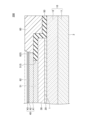
- a semiconductor device includes a substrate having a first main surface, an electrode provided above the first main surface, a first passivation layer covering the electrode and containing an inorganic material, and the first passivation layer. a second passivation layer formed on the second passivation layer and comprising an organic material, wherein a first opening is formed in the first passivation layer to expose a portion of the electrode; A second opening connected to the first opening is formed, and the first side wall surface of the first opening is inside the second side wall surface of the second opening.
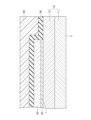
- FIG. 1 is a cross-sectional view showing the semiconductor device according to the first embodiment.
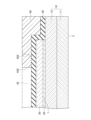
- FIG. 2 is a cross-sectional view (Part 1) showing the method of manufacturing the semiconductor device according to the first embodiment.
- FIG. 3 is a cross-sectional view (part 2) showing the method of manufacturing the semiconductor device according to the first embodiment.
- FIG. 4 is a cross-sectional view (Part 3) showing the method of manufacturing the semiconductor device according to the first embodiment.
- FIG. 5 is a cross-sectional view (part 4) showing the method for manufacturing the semiconductor device according to the first embodiment.
- FIG. 6 is a cross-sectional view (No. 5) showing the method of manufacturing the semiconductor device according to the first embodiment.
- FIG. 7 is a cross-sectional view (No.
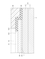
- FIG. 8 is a cross-sectional view showing the semiconductor device according to the second embodiment.
- FIG. 9 is a cross-sectional view (part 1) showing the method of manufacturing the semiconductor device according to the second embodiment.
- FIG. 10 is a cross-sectional view (part 2) showing the method of manufacturing the semiconductor device according to the second embodiment.
- FIG. 11 is a cross-sectional view (part 3) showing the method of manufacturing the semiconductor device according to the second embodiment.
- FIG. 12 is a cross-sectional view (part 4) showing the method of manufacturing the semiconductor device according to the second embodiment.
- FIG. 13 is a cross-sectional view (No. 5) showing the method of manufacturing the semiconductor device according to the second embodiment.
- the plating solution may enter the inside of the semiconductor device when forming the plating layer on the surface of the electrode.
- An object of the present disclosure is to provide a semiconductor device and a method for manufacturing a semiconductor device that can suppress penetration of a plating solution.
- a semiconductor device includes a substrate having a first main surface, an electrode provided above the first main surface, and a first passivation layer covering the electrode and containing an inorganic material. and a second passivation layer formed on the first passivation layer and containing an organic material, wherein a first opening exposing a portion of the electrode is formed in the first passivation layer, the A second opening connected to the first opening is formed in the second passivation layer, and the first side wall surface of the first opening is inside the second side wall surface of the second opening.
- the first side wall surface of the first opening is located inside the second side wall surface of the second opening, even when a plating layer is formed on the surface of the electrode, it is possible to pass through the interface between the electrode and the first passivation layer. Infiltration of all plating solutions can be suppressed.
- the plating layer can be formed on the inner portion of the second side wall surface of the first passivation layer, the volume of the plating layer can be ensured, and an increase in electrical resistance can be suppressed.
- the second passivation layer in a cross section perpendicular to the first main surface and the first side wall surface, has the above-described
- the first boundary between the second side wall surface and the first passivation layer is defined by the first passivation layer and the second passivation layer on the second side wall surface. It may be located inside the second opening from a first point separated from the interface with the layer by t 2 /2 in the direction perpendicular to the first main surface. In this case, it is easy to secure the volume inside the second opening while securing the contact area between the first passivation layer and the second passivation layer to obtain good adhesion. Further, when the mold resin is provided on the second passivation layer, it is easy to secure a contact area between the second passivation layer and the mold resin, and the adhesion can be improved.
- the angle between the straight line connecting the first boundary and the first point and the first main surface may be 85° or more and less than 90°. In this case, it is easy to ensure the thickness of the second passivation layer while avoiding an increase in area.
- the first passivation layer may include a silicon nitride layer. In this case, excellent resistance to moisture is likely to be obtained.
- the second passivation layer may include a polyimide layer. In this case, it is easy to obtain an appropriate degree of hardness on the surface.
- the substrate may be a silicon carbide substrate. In this case, it is easy to obtain excellent withstand voltage.
- a method for manufacturing a semiconductor device includes the steps of: forming an electrode above the first main surface of a substrate having a first main surface; and forming a second passivation layer containing an organic material on the first passivation layer, wherein a portion of the electrode is formed on the first passivation layer.
- a first opening is formed to be exposed, a second opening is formed in the second passivation layer and continues to the first opening, and a first side wall surface of the first opening is a second opening of the second opening. Located inside the side wall.
- the first side wall surface of the first opening is located inside the second side wall surface of the second opening, even when a plating layer is formed on the surface of the electrode, it is possible to pass through the interface between the electrode and the first passivation layer. Infiltration of all plating solutions can be suppressed.
- the plating layer can be formed on the inner portion of the second side wall surface of the first passivation layer, the volume of the plating layer can be ensured, and an increase in electrical resistance can be suppressed.
- the first opening may be formed after the second opening is formed. In this case, it is easy to form the first opening with high precision.
- a step of forming a third opening in the second passivation layer, wherein the third side wall surface of the third opening is The second opening may be formed after the first opening is formed inside the second sidewall surface of the second opening.
- the mask material for forming the first opening 51 can be omitted.
- FIG. 1 is a cross-sectional view showing the semiconductor device according to the first embodiment.
- the semiconductor device 100 mainly includes a substrate 10, an ohmic layer 20, an electrode 30, a plating layer 40, a first passivation layer 50, and a second passivation layer. 60.
- the substrate 10 is, for example, a silicon carbide substrate.
- Substrate 10 includes, for example, silicon carbide single crystal substrate 11 and silicon carbide epitaxial layer 12 on silicon carbide single crystal substrate 11 .
- the substrate 10 has a first major surface 1 and a second major surface 2 opposite the first major surface 1 .
- Silicon carbide epitaxial layer 12 forms first main surface 1
- silicon carbide single-crystal substrate 11 forms second main surface 2 .
- Silicon carbide single crystal substrate 11 and silicon carbide epitaxial layer 12 are made of hexagonal silicon carbide of polytype 4H, for example.
- a plurality of semiconductor regions doped with impurities may be formed in silicon carbide epitaxial layer 12 .
- a semiconductor element such as a field effect transistor is formed on the substrate 10 .
- the first main surface 1 is a plane in which the ⁇ 0001 ⁇ plane or the ⁇ 0001 ⁇ plane is inclined in the off direction by an off angle of 8° or less.
- the first main surface 1 is the (000-1) plane or a plane in which the (000-1) plane is inclined in the off direction by an off angle of 8° or less.
- the off direction may be, for example, the ⁇ 11-20> direction or the ⁇ 1-100> direction.
- the off angle may be, for example, 1° or more, or may be 2° or more.
- the off angle may be 6° or less, or may be 4° or less.
- Ohmic layer 20 is selectively formed on first main surface 1 and is in ohmic contact with part of silicon carbide epitaxial layer 12 .
- the ohmic layer 20 is made of a material containing nickel silicide (NiSi), for example.
- Ohmic layer 20 may be made of a material containing titanium (Ti), aluminum, and silicon.
- Electrode 30 is formed on the ohmic layer 20. Electrode 30 is, for example, an aluminum electrode. Electrode 30 is electrically connected to substrate 10 via ohmic layer 20 .
- the first passivation layer 50 contains an inorganic material.
- First passivation layer 50 is formed on silicon carbide epitaxial layer 12 and partially covers electrode 30 .
- a first opening 51 is formed in the first passivation layer 50 .
- a first opening 51 is formed on the electrode 30 , and a portion of the electrode 30 is exposed through the first opening 51 .
- the first passivation layer 50 includes, for example, a silicon nitride (SiN) layer.
- the first passivation layer 50 may be a silicon nitride layer.
- the first opening 51 has a first side wall surface 51S.
- the first side wall surface 51S may be perpendicular to the first principal surface 1 or may be inclined from a plane perpendicular to the first principal surface 1 .
- the second passivation layer 60 contains an organic material.
- a second passivation layer 60 is formed over the first passivation layer 50 .
- a second opening 61 that continues to the first opening 51 is formed in the second passivation layer 60 .
- a second opening 61 is formed on the first passivation layer 50 , and a portion of the first passivation layer 50 and a portion of the electrode 30 are exposed through the second opening 61 .
- the second opening 61 has a second side wall surface 61S. In plan view from a direction perpendicular to the first main surface 1, the first side wall surface 51S is inside the second side wall surface 61S.
- the second side wall surface 61S may be perpendicular to the first major surface 1 .
- the second passivation layer 60 includes, for example, a polyimide layer.
- the second passivation layer 60 may be a polyimide layer.
- the plating layer 40 has a nickel (Ni) plating layer 41 , a palladium (Pd) plating layer 42 and a gold (Au) plating layer 43 .
- the Ni plating layer 41 is formed on the electrode 30 inside the first opening 51 and the second opening 61 .
- the Ni plating layer 41 may contain phosphorus (P).
- the Pd plating layer 42 is formed on the Ni plating layer 41 inside the second opening 61 .
- the Au plating layer 43 is formed on the Pd plating layer 42 inside the second opening 61 .
- the thickness of the Ni plating layer 41 is preferably 3.0 ⁇ m or more and 7.0 ⁇ m or less, more preferably 4.0 ⁇ m or more and 6.0 ⁇ m or less.
- the thickness of the Pd plating layer 42 is preferably 20 nm or more and 40 nm or less, more preferably 25 nm or more and 35 nm or less.
- the thickness of the Au plating layer 43 is preferably 30 nm or more and 70 nm or less, more preferably 40 nm or more and 60 nm or less.
- 2 to 7 are cross-sectional views showing the method of manufacturing the semiconductor device 100 according to the first embodiment.
- a substrate 10 is prepared.
- silicon carbide epitaxial layer 12 is formed on silicon carbide single crystal substrate 11 .
- various semiconductor regions are formed in the silicon carbide epitaxial layer 12 by ion implantation or the like.
- an ohmic layer 20 is formed on the first main surface 1 and an electrode 30 is formed on the ohmic layer 20 .
- a first passivation layer 50 is formed on the first main surface 1 so as to cover the ohmic layer 20 and the electrode 30 .
- the first passivation layer 50 for example, a silicon nitride layer is formed.
- a second passivation layer 60 is then formed on the first passivation layer 50 .
- a polyimide layer is formed.
- a second opening 61 is formed in the second passivation layer 60 .
- the second opening 61 has a second side wall surface 61S.
- the second passivation layer 60 is a photosensitive polyimide layer, exposing and developing the second passivation layer 60 can form the second openings 61 .
- a mask 110 having openings 111 is formed on the first passivation layer 50 and the second passivation layer 60 .
- Mask 110 is, for example, a resist mask.
- the opening 111 has side wall surfaces 111S. In plan view from the direction perpendicular to the first main surface 1, the side wall surface 111S is inside the second side wall surface 61S.
- the first passivation layer 50 is etched using a mask 110 to form a first opening 51 in the first passivation layer 50 .
- this etching for example, dry etching is performed using a mixed gas of carbon tetrafluoride (CF 4 ) and oxygen (O 2 ) while applying a bias voltage.
- the mask 110 is removed.
- a plating layer 40 is formed.
- a plating solution is used to form a Ni plating layer 41, a Pd plating layer 42 and an Au plating layer 43 in this order.
- the semiconductor device 100 according to the first embodiment can be manufactured.
- the first side wall surface 51S of the first opening 51 is inside the second side wall surface 61S of the second opening 61. Therefore, when the plating layer 40 is formed, the plating solution can be prevented from entering the first main surface 1 through the interface between the electrode 30 and the first passivation layer 50 . In addition, since the plating layer 40 can be formed on the portion of the first passivation layer 50 inside the second side wall surface 61S, the volume of the plating layer 40 can be secured and an increase in electrical resistance can be suppressed.
- the silicon nitride layer in the first passivation layer 50 By including the silicon nitride layer in the first passivation layer 50, excellent resistance to moisture can be obtained.
- the second passivation layer 60 includes a polyimide layer, the surface can be provided with appropriate hardness. Further, since the substrate 10 is a silicon carbide substrate, excellent breakdown voltage can be obtained.
- the first opening 51 in the first passivation layer 50 after forming the second opening 61 in the second passivation layer 60, it is easy to form the first opening 51 with high precision.
- the distance L1 in the direction parallel to the first main surface 1 between the first boundary 71 with the passivation layer 50 and the second boundary 72 between the first side wall surface 51S and the electrode 30 is preferably 5 ⁇ t 1 or less. This is because if the distance L 1 exceeds 5 ⁇ t 1 , the volume inside the first opening 51 becomes too small, making it difficult to secure the volume of the plating layer 40, and the electrical resistance of the plating layer 40 increases. This is because there is a risk of The distance L1 is more preferably 4 ⁇ t1 or less, and even more preferably 3 ⁇ t1 or less.
- FIG. 8 is a cross-sectional view showing the semiconductor device according to the second embodiment.
- a second opening 62 is formed in the second passivation layer 60 instead of the second opening 61 .
- the second opening 62 continues to the first opening 51 and is formed on the first passivation layer 50 . and a portion of the electrode 30 are exposed.
- the second opening 62 has a second side wall surface 62S.
- the first side wall surface 51S is inside the second side wall surface 62S.
- the second side wall surface 62S may not be perpendicular to the first main surface 1 and may include a curved surface.
- the second side wall surface 62S may be a plane inclined from a plane perpendicular to the first main surface 1 .
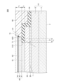
- the maximum thickness of the portion of the second passivation layer 60 overlapping the electrode 30 in plan view from the direction perpendicular to the first main surface 1 is t2 . do.
- a point on the second side wall surface 62S which is separated from the interface between the first passivation layer 50 and the second passivation layer 60 by t 2 /2 in the direction perpendicular to the first main surface 1 is the first point. 81.
- the first boundary 71 is located inside the second opening 62 with respect to the first point 81 .
- the second side wall surface 62S is inclined such that the closer the position to the first main surface 1, the narrower the second opening 62 becomes.
- 9 to 13 are cross-sectional views showing the manufacturing method of the semiconductor device 200 according to the second embodiment.
- a third opening 63 is formed in the second passivation layer 60 .
- the third opening 63 has a third side wall surface 63S.
- the second passivation layer 60 is a photosensitive polyimide layer, exposing and developing the second passivation layer 60 can form the third openings 63 .
- the third opening 63 is formed such that the third side wall surface 63S is located inside the second side wall surface 62S when the second opening 62 is formed.
- the first passivation layer 50 is etched to form a first opening 51 in the first passivation layer 50 .
- this etching for example, dry etching using a mixed gas of carbon tetrafluoride (CF 4 ) and oxygen (O 2 ) is performed without applying a bias voltage.
- This etching is, for example, isotropic etching.
- the first opening 51 is formed, for example, so that the first side wall surface 51S is positioned outside the third side wall surface 63S in plan view from a direction perpendicular to the first principal surface 1 .
- a mask 210 having openings 211 is formed on the second passivation layer 60.
- Mask 210 is, for example, a resist mask.
- the opening 211 has side wall surfaces 211S. In plan view from the direction perpendicular to the first main surface 1, the side wall surface 211S is inside the first side wall surface 51S.
- the second passivation layer 60 is etched using a mask 210 to form a second opening 62 in the second passivation layer 60 .
- a mask 210 may be removed during this wet etching.
- a stripping liquid for removing the mask 210 for example, an aqueous solution of tetramethylammonium hydroxide (TMAH) can be used.
- TMAH tetramethylammonium hydroxide
- a plating layer 40 is formed.
- a plating solution is used to form a Ni plating layer 41, a Pd plating layer 42 and an Au plating layer 43 in this order.
- the semiconductor device 200 according to the second embodiment can be manufactured.
- the first side wall surface 51S of the first opening 51 is inside the second side wall surface 62S of the second opening 62 . Therefore, when the plating layer 40 is formed, the plating solution can be prevented from entering the first main surface 1 through the interface between the electrode 30 and the first passivation layer 50 . In addition, since the plating layer 40 can be formed on the portion of the first passivation layer 50 inside the second side wall surface 61S, the volume of the plating layer 40 can be secured and an increase in electrical resistance can be suppressed.
- the contact area between the first passivation layer 50 and the second passivation layer 60 is ensured to obtain good adhesion, while the It is easy to secure the volume inside the two openings 62 . Further, when the mold resin is provided on the second passivation layer 60, it is easy to secure the contact area between the second passivation layer 60 and the mold resin, and the adhesion can be improved.
- the first opening 51 is formed in the first passivation layer 50 using the second passivation layer 60 as a mask. can omit the mask material for
- the angle ⁇ between the straight line 73 connecting the first boundary 71 and the first point 81 and the first main surface 1 is preferably 85° or more and less than 90°. If the angle ⁇ is less than 85°, the inclination of the second side wall surface 62S becomes excessively gentle, and a large area may be required to obtain the second passivation layer 60 with a desired thickness. This is because
- An electrode may be provided on the first main surface 1 separately from the electrode 30, and another electrode may be provided on the second main surface 2.
- the electrode 30 may be the source electrode
- the other electrode on the first major surface 1 may be the gate electrode
- the electrode on the second major surface 2 may be the drain electrode.
- the material of the first passivation layer 50 may be silicon oxide or silicon oxynitride, for example.
- the second side wall surface 61S of the second passivation layer 60 may be curved or the second side wall surface 62S may be inclined as in the second embodiment. good too.
Landscapes
- Internal Circuitry In Semiconductor Integrated Circuit Devices (AREA)
Priority Applications (1)
| Application Number | Priority Date | Filing Date | Title |
|---|---|---|---|
| JP2023554999A JPWO2023067925A1 (https=) | 2021-10-21 | 2022-09-06 |
Applications Claiming Priority (2)
| Application Number | Priority Date | Filing Date | Title |
|---|---|---|---|
| JP2021-172673 | 2021-10-21 | ||
| JP2021172673 | 2021-10-21 |
Publications (1)
| Publication Number | Publication Date |
|---|---|
| WO2023067925A1 true WO2023067925A1 (ja) | 2023-04-27 |
Family
ID=86058989
Family Applications (1)
| Application Number | Title | Priority Date | Filing Date |
|---|---|---|---|
| PCT/JP2022/033368 Ceased WO2023067925A1 (ja) | 2021-10-21 | 2022-09-06 | 半導体装置及び半導体装置の製造方法 |
Country Status (2)
| Country | Link |
|---|---|
| JP (1) | JPWO2023067925A1 (https=) |
| WO (1) | WO2023067925A1 (https=) |
Citations (4)
| Publication number | Priority date | Publication date | Assignee | Title |
|---|---|---|---|---|
| JP2013239607A (ja) * | 2012-05-16 | 2013-11-28 | Mitsubishi Electric Corp | 半導体装置 |
| JP2015170857A (ja) * | 2014-03-07 | 2015-09-28 | インフィネオン テクノロジーズ アーゲーInfineon Technologies Ag | パッシベーション層を有する半導体素子およびその生産方法 |
| JP2017069381A (ja) * | 2015-09-30 | 2017-04-06 | ルネサスエレクトロニクス株式会社 | 半導体装置および半導体装置の製造方法 |
| WO2021065722A1 (ja) * | 2019-09-30 | 2021-04-08 | ローム株式会社 | 半導体装置 |
-
2022
- 2022-09-06 JP JP2023554999A patent/JPWO2023067925A1/ja active Pending
- 2022-09-06 WO PCT/JP2022/033368 patent/WO2023067925A1/ja not_active Ceased
Patent Citations (4)
| Publication number | Priority date | Publication date | Assignee | Title |
|---|---|---|---|---|
| JP2013239607A (ja) * | 2012-05-16 | 2013-11-28 | Mitsubishi Electric Corp | 半導体装置 |
| JP2015170857A (ja) * | 2014-03-07 | 2015-09-28 | インフィネオン テクノロジーズ アーゲーInfineon Technologies Ag | パッシベーション層を有する半導体素子およびその生産方法 |
| JP2017069381A (ja) * | 2015-09-30 | 2017-04-06 | ルネサスエレクトロニクス株式会社 | 半導体装置および半導体装置の製造方法 |
| WO2021065722A1 (ja) * | 2019-09-30 | 2021-04-08 | ローム株式会社 | 半導体装置 |
Also Published As
| Publication number | Publication date |
|---|---|
| JPWO2023067925A1 (https=) | 2023-04-27 |
Similar Documents
| Publication | Publication Date | Title |
|---|---|---|
| US11145711B2 (en) | Capacitor and method for manufacturing capacitor | |
| JP4435864B2 (ja) | 半導体素子 | |
| CN102569307B (zh) | 薄膜晶体管基板及其制造方法 | |
| CN111584364B (zh) | 半导体装置的制造方法及半导体装置 | |
| WO2013161450A1 (ja) | 炭化珪素半導体素子の製造方法 | |
| US11476110B2 (en) | Semiconductor device | |
| US8563404B2 (en) | Process for dividing wafer into individual chips and semiconductor chips | |
| WO2023067925A1 (ja) | 半導体装置及び半導体装置の製造方法 | |
| US20040016940A1 (en) | Semiconductor device | |
| WO2023067926A1 (ja) | 半導体装置 | |
| JP7070392B2 (ja) | 半導体装置の製造方法 | |
| JP3872031B2 (ja) | 半導体装置の製造方法 | |
| JP2007019102A (ja) | 半導体装置の製造方法 | |
| US20260068265A1 (en) | Semiconductor device | |
| US20240379784A1 (en) | Semiconductor device and method for manufacturing semiconductor device | |
| US6174792B1 (en) | Method of manufacturing a semiconductor device | |
| TW202611948A (zh) | 半導體裝置 | |
| KR20040084471A (ko) | 반도체소자의 퓨즈부 형성방법 | |
| JP2008072026A (ja) | 半導体装置の製造方法及び半導体装置 | |
| JPH0334856B2 (https=) | ||
| JPS5923101B2 (ja) | 半導体装置の製造方法 | |
| JPS60113965A (ja) | 半導体装置 | |
| JPS6227754B2 (https=) | ||
| JPH0265141A (ja) | 半導体装置の製造方法 | |
| JPS6053019A (ja) | 半導体装置の製造方法 |
Legal Events
| Date | Code | Title | Description |
|---|---|---|---|
| 121 | Ep: the epo has been informed by wipo that ep was designated in this application |
Ref document number: 22883236 Country of ref document: EP Kind code of ref document: A1 |
|
| WWE | Wipo information: entry into national phase |
Ref document number: 2023554999 Country of ref document: JP |
|
| NENP | Non-entry into the national phase |
Ref country code: DE |
|
| 122 | Ep: pct application non-entry in european phase |
Ref document number: 22883236 Country of ref document: EP Kind code of ref document: A1 |