US6174792B1 - Method of manufacturing a semiconductor device - Google Patents
Method of manufacturing a semiconductor device Download PDFInfo
- Publication number
- US6174792B1 US6174792B1 US09/110,180 US11018098A US6174792B1 US 6174792 B1 US6174792 B1 US 6174792B1 US 11018098 A US11018098 A US 11018098A US 6174792 B1 US6174792 B1 US 6174792B1
- Authority
- US
- United States
- Prior art keywords
- film
- oxide film
- nitride film
- gate electrode
- nitride
- Prior art date
- Legal status (The legal status is an assumption and is not a legal conclusion. Google has not performed a legal analysis and makes no representation as to the accuracy of the status listed.)
- Expired - Fee Related
Links
Images


Classifications
-
- H—ELECTRICITY
- H10—SEMICONDUCTOR DEVICES; ELECTRIC SOLID-STATE DEVICES NOT OTHERWISE PROVIDED FOR
- H10D—INORGANIC ELECTRIC SEMICONDUCTOR DEVICES
- H10D30/00—Field-effect transistors [FET]
- H10D30/01—Manufacture or treatment
- H10D30/021—Manufacture or treatment of FETs having insulated gates [IGFET]
- H10D30/0221—Manufacture or treatment of FETs having insulated gates [IGFET] having asymmetry in the channel direction, e.g. lateral high-voltage MISFETs having drain offset region or extended-drain MOSFETs [EDMOS]
-
- H—ELECTRICITY
- H10—SEMICONDUCTOR DEVICES; ELECTRIC SOLID-STATE DEVICES NOT OTHERWISE PROVIDED FOR
- H10D—INORGANIC ELECTRIC SEMICONDUCTOR DEVICES
- H10D30/00—Field-effect transistors [FET]
- H10D30/60—Insulated-gate field-effect transistors [IGFET]
- H10D30/601—Insulated-gate field-effect transistors [IGFET] having lightly-doped drain or source extensions, e.g. LDD IGFETs or DDD IGFETs
- H10D30/603—Insulated-gate field-effect transistors [IGFET] having lightly-doped drain or source extensions, e.g. LDD IGFETs or DDD IGFETs having asymmetry in the channel direction, e.g. lateral high-voltage MISFETs having drain offset region or extended drain IGFETs [EDMOS]
-
- H—ELECTRICITY
- H10—SEMICONDUCTOR DEVICES; ELECTRIC SOLID-STATE DEVICES NOT OTHERWISE PROVIDED FOR
- H10D—INORGANIC ELECTRIC SEMICONDUCTOR DEVICES
- H10D64/00—Electrodes of devices having potential barriers
- H10D64/20—Electrodes characterised by their shapes, relative sizes or dispositions
- H10D64/27—Electrodes not carrying the current to be rectified, amplified, oscillated or switched, e.g. gates
- H10D64/311—Gate electrodes for field-effect devices
- H10D64/411—Gate electrodes for field-effect devices for FETs
- H10D64/511—Gate electrodes for field-effect devices for FETs for IGFETs
- H10D64/514—Gate electrodes for field-effect devices for FETs for IGFETs characterised by the insulating layers
- H10D64/516—Gate electrodes for field-effect devices for FETs for IGFETs characterised by the insulating layers the thicknesses being non-uniform
Definitions
- the present invention relates to a method of manufacturing a semiconductor device such as a power IC which includes lateral unit structures with high breakdown voltage. More specifically, the present invention relates to a method of manufacturing a semiconductor device which exhibits a breakdown voltage of 20 V or more.
- a plurality of high-breakdown-voltage devices are integrated on one single chip.
- a drain side portion of a gate electrode is extended onto a LOCOS (local oxidation of silicon) film for device separation to relax the electric field localization below the drain-side edge of the gate electrode.
- LOCOS local oxidation of silicon
- each high-breakdown-voltage device integrated on a chip has become so fine that the size of the constituent device affects greatly the down-sizing of the chip.
- the LOCOS film for electric field relaxation is formed through an exclusive mask, an alignment mismatch of around 0.3 ⁇ m is caused between the LOCOS film and the gate electrode, and the LOCOS film is elongated by the alignment mismatch.
- the device pitch distance between the source and the drain
- the chip size increases to 4.3 ⁇ m, i.e. around 8% (0.3 ⁇ m+4 ⁇ m).
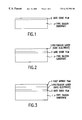
- FIG. 11 is a cross section of a main portion of a conventional lateral type DMOSFET with a high breakdown voltage.
- a p-type base region 23 and an n-type offset region 21 are formed in the surface portion of a p-type silicon substrate 1 .
- An n-type source region 24 is formed in the surface portion of the p-type base region 23 .
- a polysilicon gate electrode 27 a is formed above the p-type base region 23 and the p-type silicon substrate 1 between the n-type source region 24 and the n-type offset region 21 with a gate oxide film 2 interposed inbetween.
- the gate electrode 27 a is extended onto a part of a LOCOS film 6 a formed on the n-type offset region 21 .
- n-type drain region 22 and a drain electrode 25 are formed on the right hand side of the n-type offset region 21 . Since LOCOS film 6 a and gate electrode 27 a are patterned through individual or different masks, the foregoing patterning mismatch (alignment mismatch) occurs. Due to the alignment mismatch, the overlap length D of the gate electrode 27 a and LOCOS film 6 a is elongated. As the overlap length D becomes longer, it is necessary to elongate the LOCOS film 6 a for obtaining the design value of the breakdown voltage. As the device structure becomes finer as described above, the alignment mismatch can not be ignored. The device pitch (distance between the source and the drain) W becomes longer by the increment of the length of the LOCOS film 6 . The elongated device pitch enlarges the chip size.
- the conventional technique causes the alignment mismatch as the device structure becomes finer.
- the alignment mismatch further causes the chip size increase.
- a method of manufacturing a semiconductor device including the steps of: forming a gate oxide film on a semiconductor substrate; forming a gate electrode on the gate oxide film; forming a first nitride film on the gate electrode; etching the gate electrode and the first nitride film through a same mask; depositing a second nitride film for covering at least a side wall of the gate electrode; forming an opening in the second nitride film by anisotropic etching such that the second nitride film is left on the side wall of the gate electrode; and forming a thick oxide film in the bottom of the opening in the second nitride film by thermal oxidation.
- the alignment mismatch between the gate electrode and the oxide film for the electric field relaxation is prevented by forming the gate electrode and the oxide film through the same mask.
- the first nitride film is deposited to prevent the gate electrode of polysilicon from being oxidized.
- the second nitride film left on the side wall of the gate electrode by anisotropic etching also prevents the gate electrode from being oxidized.
- the thick oxide film is a LOCOS film for device separation.
- the semiconductor device according to the invention is of a lateral type.
- the thick oxide film is formed for relaxing the electric field below the drain-side edge of the gate electrode.
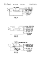
- FIGS. 1 through 9 are cross sectional views illustrating the manufacturing steps of a semiconductor device according to an embodiment of the invention.
- FIG. 10 is a cross sectional view of a main portion of a lateral type semiconductor device exhibiting a high breakdown voltage according to another embodiment of the invention.
- FIG. 11 is a cross sectional view of a main portion of a conventional lateral type DMOSFET with a high breakdown voltage.
- FIGS. 1 through 9 are cross sectional views illustrating the manufacturing steps of a semiconductor device according to the embodiment of the invention.
- a gate oxide film 2 of 200 ⁇ in thickness is formed on a p-type silicon substrate 1 .
- a polysilicon layer 3 of 3000 ⁇ in thickness for a gate electrode is formed on the gate oxide film 2 .
- a first nitride film 4 of 3000 ⁇ in thickness is deposited on the polysilicon layer 3 .
- the polysilicon layer 3 and the first nitride film 4 are etched with a LOCOS film forming pattern such that a first opening is formed.
- a second nitride film 5 of 1000 ⁇ in thickness is deposited such that the second nitride film 5 covers at least the polysilicon layer 3 .
- the second nitride film 5 is etched by an anisotropic etching. After the anisotropic etching, the etched surface of the polysilicon layer 3 is still covered with the second nitride film 5 , but the surface of the gate oxide film 2 is exposed to a second opening 12 .
- the width L of the second nitride film 5 in the form of a spacer is 1000 ⁇ or less.
- a LOCOS film of 6000 ⁇ in thickness is formed by using the protected polysilicon layer 3 as a mask as shown in FIG. 7 .
- the distance d between the polysilicon layer 3 and the LOCOS film 6 is determined by the variation of the width L caused by the variation of the etching condition.
- its bird's beak i.e. length of a gradually thinning portion of the LOCOS film, is around 0.5 ⁇ m. Therefore, the LOCOS film 6 is sufficiently extended deeply below the polysilicon layer 3 .
- a polysilicon self-alignment film that is the LOCOS film 6
- a polysilicon self-alignment film that is the LOCOS film 6
- a polysilicon layer 3 b not used as a gate electrode, and a portion of a polysilicon layer 3 a used as a gate electrode and located at the opposite side of the LOCOS film 6 are removed by etching as shown in FIG. 9 .
- An n-type substrate may be used without problems for the substrate 1 .
- FIG. 10 is a cross sectional view of the main portion of a lateral type semiconductor device exhibiting a high breakdown voltage according to another embodiment of the invention.
- a LOCOS film 6 ′ is formed on an n-type offset region 21 , in contrast to the LOCOS film 6 formed on the p-type silicon substrate 1 in FIGS. 1 through 9.
- the lateral type semiconductor device of FIG. 10 is different from the conventional lateral type semiconductor device of FIG. 11 in that the LOCOS film 6 ′ of FIG. 10 on the n-type offset region 21 is patterned simultaneously with the patterning of a gate electrode 27 . Therefore, in the lateral type semiconductor device of FIG. 10, any alignment mismatch is not caused between the LOCOS film and the gate electrode, and the overlap length d of the LOCOS film and the gate electrode is half or less than the overlap length in the conventional device.
- the LOCOS film 6 ′ of FIG. 10 is formed by the self-alignment, while the LOCOS film 6 a of FIG. 11 is not.
- the gate length is shortened to 1.0 ⁇ m, the oxide film width to 0.6 Mm and the device pitch (distance between the source and the drain) w from 4.3 ⁇ m to 4.0 ⁇ m.
- dislocation or misalignment of the gate electrode and the LOCOS film is prevented by employing the self-alignment technique.
- the gate length, and therefore, the device pitch is shortened, and the chip size is reduced.
Landscapes
- Local Oxidation Of Silicon (AREA)
- Element Separation (AREA)
- Insulated Gate Type Field-Effect Transistor (AREA)
Abstract
A semiconductor device is manufactured by forming a gate oxide film on a semiconductor substrate; forming a gate electrode on the gate oxide film; forming a first nitride film on the gate electrode; etching the gate electrode and the first nitride film through a same mask; depositing a second nitride film on at least a side wall of the gate electrode for covering the same; forming an opening in the second nitride film by etching such that the second nitride film is left on the side wall of the gate electrode; and forming a thick oxide film, i.e. LOCOS film, on a bottom of the opening in the second nitride film by a thermal oxidation. The alignment mismatch between the LOCOS film and the gate electrode is prevented, and the overlap length of the LOCOS film and the gate electrode is shortened to a half or less of the overlap length in the conventional device.
Description
The present invention relates to a method of manufacturing a semiconductor device such as a power IC which includes lateral unit structures with high breakdown voltage. More specifically, the present invention relates to a method of manufacturing a semiconductor device which exhibits a breakdown voltage of 20 V or more.
In many conventional power IC's, a plurality of high-breakdown-voltage devices are integrated on one single chip. In the high-breakdown-voltage device, a drain side portion of a gate electrode is extended onto a LOCOS (local oxidation of silicon) film for device separation to relax the electric field localization below the drain-side edge of the gate electrode.
Recently, the structure of each high-breakdown-voltage device integrated on a chip has become so fine that the size of the constituent device affects greatly the down-sizing of the chip. When the LOCOS film for electric field relaxation is formed through an exclusive mask, an alignment mismatch of around 0.3 μm is caused between the LOCOS film and the gate electrode, and the LOCOS film is elongated by the alignment mismatch. When the device pitch (distance between the source and the drain) is 4 μm, for example, the chip size increases to 4.3 μm, i.e. around 8% (0.3 μm+4 μm).
FIG. 11 is a cross section of a main portion of a conventional lateral type DMOSFET with a high breakdown voltage. Here, the DMOSFET strands for “dual diffusion metal oxide semiconductor field effect transistor”.
Referring now to FIG. 11, a p-type base region 23 and an n-type offset region 21 are formed in the surface portion of a p-type silicon substrate 1. An n-type source region 24 is formed in the surface portion of the p-type base region 23. A polysilicon gate electrode 27 a is formed above the p-type base region 23 and the p-type silicon substrate 1 between the n-type source region 24 and the n-type offset region 21 with a gate oxide film 2 interposed inbetween. The gate electrode 27 a is extended onto a part of a LOCOS film 6 a formed on the n-type offset region 21. An n-type drain region 22 and a drain electrode 25 are formed on the right hand side of the n-type offset region 21. Since LOCOS film 6 a and gate electrode 27 a are patterned through individual or different masks, the foregoing patterning mismatch (alignment mismatch) occurs. Due to the alignment mismatch, the overlap length D of the gate electrode 27 a and LOCOS film 6 a is elongated. As the overlap length D becomes longer, it is necessary to elongate the LOCOS film 6 a for obtaining the design value of the breakdown voltage. As the device structure becomes finer as described above, the alignment mismatch can not be ignored. The device pitch (distance between the source and the drain) W becomes longer by the increment of the length of the LOCOS film 6. The elongated device pitch enlarges the chip size.
As described above, the conventional technique causes the alignment mismatch as the device structure becomes finer. The alignment mismatch further causes the chip size increase.
In view of the foregoing, it is an object of the invention to provide a method of manufacturing a lateral type semiconductor device which facilitates shortening the device pitch without enlarging the chip size.
According to an aspect of the invention, there is provided a method of manufacturing a semiconductor device, the method including the steps of: forming a gate oxide film on a semiconductor substrate; forming a gate electrode on the gate oxide film; forming a first nitride film on the gate electrode; etching the gate electrode and the first nitride film through a same mask; depositing a second nitride film for covering at least a side wall of the gate electrode; forming an opening in the second nitride film by anisotropic etching such that the second nitride film is left on the side wall of the gate electrode; and forming a thick oxide film in the bottom of the opening in the second nitride film by thermal oxidation.
The alignment mismatch between the gate electrode and the oxide film for the electric field relaxation is prevented by forming the gate electrode and the oxide film through the same mask. The first nitride film is deposited to prevent the gate electrode of polysilicon from being oxidized. And, the second nitride film left on the side wall of the gate electrode by anisotropic etching also prevents the gate electrode from being oxidized.
Advantageously, the thick oxide film is a LOCOS film for device separation.
By employing the LOCOS technique, a thick oxide film is obtained without adding any manufacturing step of thickening an oxide film. The semiconductor device according to the invention is of a lateral type.
Advantageously, the thick oxide film is formed for relaxing the electric field below the drain-side edge of the gate electrode.
FIGS. 1 through 9 are cross sectional views illustrating the manufacturing steps of a semiconductor device according to an embodiment of the invention;
FIG. 10 is a cross sectional view of a main portion of a lateral type semiconductor device exhibiting a high breakdown voltage according to another embodiment of the invention; and
FIG. 11 is a cross sectional view of a main portion of a conventional lateral type DMOSFET with a high breakdown voltage.
Now the present invention will be described hereinafter with reference to the accompanying drawings which illustrate the preferred embodiments of the invention.
FIGS. 1 through 9 are cross sectional views illustrating the manufacturing steps of a semiconductor device according to the embodiment of the invention.
In FIG. 1, a gate oxide film 2 of 200 Å in thickness is formed on a p-type silicon substrate 1. In FIG. 2, a polysilicon layer 3 of 3000 Å in thickness for a gate electrode is formed on the gate oxide film 2. In FIG. 3, a first nitride film 4 of 3000 Å in thickness is deposited on the polysilicon layer 3. In FIG. 4, the polysilicon layer 3 and the first nitride film 4 are etched with a LOCOS film forming pattern such that a first opening is formed. In FIG. 5, a second nitride film 5 of 1000 Å in thickness is deposited such that the second nitride film 5 covers at least the polysilicon layer 3. In FIG. 6, the second nitride film 5 is etched by an anisotropic etching. After the anisotropic etching, the etched surface of the polysilicon layer 3 is still covered with the second nitride film 5, but the surface of the gate oxide film 2 is exposed to a second opening 12. The width L of the second nitride film 5 in the form of a spacer (similar to the spacer used in a LDD-MOS), is 1000 Å or less.
After protecting the exposed surface of the polysilicon layer 3 as shown in FIG. 6, a LOCOS film of 6000 Å in thickness is formed by using the protected polysilicon layer 3 as a mask as shown in FIG. 7. The distance d between the polysilicon layer 3 and the LOCOS film 6 is determined by the variation of the width L caused by the variation of the etching condition. When the LOCOS film of 6000 Å in thickness is formed, its bird's beak, i.e. length of a gradually thinning portion of the LOCOS film, is around 0.5 μm. Therefore, the LOCOS film 6 is sufficiently extended deeply below the polysilicon layer 3. Then, a polysilicon self-alignment film, that is the LOCOS film 6, is left as shown in FIG. 8 by removing the first and second nitride films 4 and 5. Then, a polysilicon layer 3 b, not used as a gate electrode, and a portion of a polysilicon layer 3 a used as a gate electrode and located at the opposite side of the LOCOS film 6 are removed by etching as shown in FIG. 9. An n-type substrate may be used without problems for the substrate 1.
FIG. 10 is a cross sectional view of the main portion of a lateral type semiconductor device exhibiting a high breakdown voltage according to another embodiment of the invention.
Referring now to FIG. 10, a LOCOS film 6′ is formed on an n-type offset region 21, in contrast to the LOCOS film 6 formed on the p-type silicon substrate 1 in FIGS. 1 through 9. The lateral type semiconductor device of FIG. 10 is different from the conventional lateral type semiconductor device of FIG. 11 in that the LOCOS film 6′ of FIG. 10 on the n-type offset region 21 is patterned simultaneously with the patterning of a gate electrode 27. Therefore, in the lateral type semiconductor device of FIG. 10, any alignment mismatch is not caused between the LOCOS film and the gate electrode, and the overlap length d of the LOCOS film and the gate electrode is half or less than the overlap length in the conventional device. In other words, the LOCOS film 6′ of FIG. 10 is formed by the self-alignment, while the LOCOS film 6 a of FIG. 11 is not. According to the invention, the gate length is shortened to 1.0 μm, the oxide film width to 0.6 Mm and the device pitch (distance between the source and the drain) w from 4.3 μm to 4.0 μm.
According to the invention, dislocation or misalignment of the gate electrode and the LOCOS film is prevented by employing the self-alignment technique. As a result, the gate length, and therefore, the device pitch is shortened, and the chip size is reduced.
Claims (11)
1. A method of manufacturing a semiconductor device comprising:
forming a gate oxide film on a semiconductor substrate;
forming a gate electrode on the gate oxide film;
forming a first nitride film on the gate electrode;
etching the gate electrode and the first nitride film through a same mask to expose the gate oxide film on the substrate;
depositing a second nitride film on at least the gate oxide film and a side wall of the gate electrode for covering the same;
forming an opening in the second nitride film by an anisotrophic etching such that the second nitride film is left on the side wall of the gate electrode directly above a part of the gate oxide film, and a part of the gate oxide film is exposed in the opening; and
forming a thick oxide film in the gate oxide film at a bottom of the opening by a thermal oxidation so that a thinning portion of the thick oxide film is formed under the gate electrode as an overlapping portion with reference to the second nitride film on the side wall, to thereby form the overlapping portion precisely.
2. A method according to claim 1, wherein the thick oxide film is a LOCOS film for device separation.
3. A method according to claim 1, wherein the thick oxide film is formed for relaxing an electric field below a drain-side edge of the gate electrode.
4. A method according to claim 1, wherein said depositing the second nitride film on at least the side wall includes depositing the second nitride film on the first nitride film, the gate oxide film, a side wall of the first nitride wall and the side wall of the gate electrode.
5. A method according to claim 4, wherein said thick oxide film extends under the second nitride film toward the thinning portion.
6. A method according to claim 5, further comprising removing the first and second nitride films after the thick oxide film is formed.
7. A method of manufacturing a semiconductor device comprising:
forming a gate oxide film on a semiconductor substrate;
forming a polysilicon layer for a gate electrode on the gate oxide film;
forming a first nitride film on the polysilicon layer;
etching the polysilicon layer and the first nitride film by a same mask to form an opening for exposing a part of the gate oxide film;
depositing a second nitride film on the first nitride film, the part of the gate oxide film and side walls of the first nitride film and the polysilicon layer at a side of the opening;
removing the second nitride film by etching such that the second nitride film is left on the side walls of the first nitride film and the polysilicon layer; and
forming a LOCOS film in the gate oxide film located at a bottom of the opening, said LOCOS film having a thick portion with a thickness greater than that of the gate oxide film and a thinning portion extending from the thick portion to the gate oxide film to form a partial overlapping portion under the polysilicon layer with reference to the second nitride film on the side walls to thereby form the overlapping portion precisely.
8. A method according to claim 7, further comprising removing the first nitride film and the polysilicon layer except for a portion for constituting the gate electrode after the LOCOS film is formed.
9. A method according to claim 7, wherein the etching for removing the second nitride film is an anisotrophic etching.
10. A method according to claim 7, wherein said thick oxide film extends under the second nitride film toward the thinning portion.
11. A method according to claim 10, further comprising removing the first and second nitride films after the thick oxide film is formed.
Applications Claiming Priority (2)
| Application Number | Priority Date | Filing Date | Title |
|---|---|---|---|
| JP9191388A JPH1140555A (en) | 1997-07-16 | 1997-07-16 | Semiconductor device manufacturing method and semiconductor device |
| JP9-191388 | 1997-07-16 |
Publications (1)
| Publication Number | Publication Date |
|---|---|
| US6174792B1 true US6174792B1 (en) | 2001-01-16 |
Family
ID=16273780
Family Applications (1)
| Application Number | Title | Priority Date | Filing Date |
|---|---|---|---|
| US09/110,180 Expired - Fee Related US6174792B1 (en) | 1997-07-16 | 1998-07-06 | Method of manufacturing a semiconductor device |
Country Status (2)
| Country | Link |
|---|---|
| US (1) | US6174792B1 (en) |
| JP (1) | JPH1140555A (en) |
Cited By (1)
| Publication number | Priority date | Publication date | Assignee | Title |
|---|---|---|---|---|
| US20060170041A1 (en) * | 2005-01-20 | 2006-08-03 | Kabushiki Kaisha Toshiba | MOSFET and optical coupling device having the same |
Citations (2)
| Publication number | Priority date | Publication date | Assignee | Title |
|---|---|---|---|---|
| JPS61244041A (en) | 1985-04-22 | 1986-10-30 | Toshiba Corp | Manufacture of semiconductor device |
| US5248350A (en) * | 1990-11-30 | 1993-09-28 | Ncr Corporation | Structure for improving gate oxide integrity for a semiconductor formed by a recessed sealed sidewall field oxidation process |
-
1997
- 1997-07-16 JP JP9191388A patent/JPH1140555A/en active Pending
-
1998
- 1998-07-06 US US09/110,180 patent/US6174792B1/en not_active Expired - Fee Related
Patent Citations (2)
| Publication number | Priority date | Publication date | Assignee | Title |
|---|---|---|---|---|
| JPS61244041A (en) | 1985-04-22 | 1986-10-30 | Toshiba Corp | Manufacture of semiconductor device |
| US5248350A (en) * | 1990-11-30 | 1993-09-28 | Ncr Corporation | Structure for improving gate oxide integrity for a semiconductor formed by a recessed sealed sidewall field oxidation process |
Cited By (1)
| Publication number | Priority date | Publication date | Assignee | Title |
|---|---|---|---|---|
| US20060170041A1 (en) * | 2005-01-20 | 2006-08-03 | Kabushiki Kaisha Toshiba | MOSFET and optical coupling device having the same |
Also Published As
| Publication number | Publication date |
|---|---|
| JPH1140555A (en) | 1999-02-12 |
Similar Documents
| Publication | Publication Date | Title |
|---|---|---|
| US6939776B2 (en) | Semiconductor device and a method of fabricating the same | |
| JP2000114463A (en) | Semiconductor device | |
| US10586735B2 (en) | Semiconductor device structure including high voltage MOS device | |
| US7528041B2 (en) | Method of manufacturing semiconductor device that utilizes oxidation prevention film to form thick and thin gate insulator portions | |
| JP2002270850A (en) | Double gate field effect transistor | |
| US7141862B2 (en) | Semiconductor device and method for manufacturing the same | |
| JP2619340B2 (en) | High voltage transistor structure of semiconductor device and method of manufacturing the same | |
| US20050087835A1 (en) | Semiconductor device and manufacturing method of the same | |
| US6174792B1 (en) | Method of manufacturing a semiconductor device | |
| CN100547763C (en) | Method for forming semiconductor device | |
| US5523250A (en) | Method of manufacturing a MOSFET with LDD regions | |
| KR100591184B1 (en) | How to Form Dual Buzz Vicrocos Device Isolation | |
| KR100790261B1 (en) | DMOS device manufacturing method | |
| JPS6119174A (en) | Semiconductor device | |
| JPH08181223A (en) | Method for manufacturing semiconductor device | |
| US8044487B2 (en) | Semiconductor device and method of manufacturing the same | |
| JPH09289305A (en) | Semiconductor device | |
| KR0147428B1 (en) | High integrated semiconductor device and the manufacturing method thereof | |
| JPH09289304A (en) | Semiconductor device | |
| JPH05283680A (en) | Mos-type semiconductor device and its production | |
| JPH08330578A (en) | Field effect high breakdown voltage transistor and method of manufacturing the same | |
| KR0151226B1 (en) | Method of device isolating layer for semiconductor device | |
| JP5187988B2 (en) | Semiconductor device and manufacturing method thereof | |
| KR970005703B1 (en) | Semiconductor device having trench type isolation structure and manufacturing method | |
| JP7269743B2 (en) | Semiconductor device and method for manufacturing semiconductor device |
Legal Events
| Date | Code | Title | Description |
|---|---|---|---|
| AS | Assignment |
Owner name: FUJI ELECTRIC CO., LTD., JAPAN Free format text: ASSIGNMENT OF ASSIGNORS INTEREST;ASSIGNOR:KITAMURA, AKIO;REEL/FRAME:009760/0848 Effective date: 19980805 |
|
| FEPP | Fee payment procedure |
Free format text: PAYOR NUMBER ASSIGNED (ORIGINAL EVENT CODE: ASPN); ENTITY STATUS OF PATENT OWNER: LARGE ENTITY |
|
| REMI | Maintenance fee reminder mailed | ||
| LAPS | Lapse for failure to pay maintenance fees | ||
| STCH | Information on status: patent discontinuation |
Free format text: PATENT EXPIRED DUE TO NONPAYMENT OF MAINTENANCE FEES UNDER 37 CFR 1.362 |
|
| FP | Lapsed due to failure to pay maintenance fee |
Effective date: 20050116 |