WO2023063348A1 - Film mince d'oxyde cristallin, stratifié et transistor à couches minces - Google Patents
Film mince d'oxyde cristallin, stratifié et transistor à couches minces Download PDFInfo
- Publication number
- WO2023063348A1 WO2023063348A1 PCT/JP2022/038036 JP2022038036W WO2023063348A1 WO 2023063348 A1 WO2023063348 A1 WO 2023063348A1 JP 2022038036 W JP2022038036 W JP 2022038036W WO 2023063348 A1 WO2023063348 A1 WO 2023063348A1
- Authority
- WO
- WIPO (PCT)
- Prior art keywords
- thin film
- oxide thin
- crystalline oxide
- region
- carrier concentration
- Prior art date
Links
- 239000010409 thin film Substances 0.000 title claims abstract description 390
- 239000005001 laminate film Substances 0.000 title 1
- 230000007480 spreading Effects 0.000 claims abstract description 47
- 238000003892 spreading Methods 0.000 claims abstract description 47
- 239000010408 film Substances 0.000 claims description 146
- 239000013078 crystal Substances 0.000 claims description 86
- 239000000758 substrate Substances 0.000 claims description 82
- 229910052760 oxygen Inorganic materials 0.000 claims description 37
- 238000000034 method Methods 0.000 claims description 31
- 229910052782 aluminium Inorganic materials 0.000 claims description 25
- 229910052710 silicon Inorganic materials 0.000 claims description 21
- 239000000470 constituent Substances 0.000 claims description 19
- 229910052739 hydrogen Inorganic materials 0.000 claims description 18
- 229910052725 zinc Inorganic materials 0.000 claims description 18
- 229910052749 magnesium Inorganic materials 0.000 claims description 17
- 229910052718 tin Inorganic materials 0.000 claims description 17
- 229910052758 niobium Inorganic materials 0.000 claims description 15
- 229910052719 titanium Inorganic materials 0.000 claims description 15
- 229910052721 tungsten Inorganic materials 0.000 claims description 15
- 229910052726 zirconium Inorganic materials 0.000 claims description 15
- 238000010894 electron beam technology Methods 0.000 claims description 14
- 229910052735 hafnium Inorganic materials 0.000 claims description 13
- 229910052750 molybdenum Inorganic materials 0.000 claims description 13
- 229910052706 scandium Inorganic materials 0.000 claims description 13
- 229910052727 yttrium Inorganic materials 0.000 claims description 13
- 229910052796 boron Inorganic materials 0.000 claims description 11
- 229910052731 fluorine Inorganic materials 0.000 claims description 10
- 229910052733 gallium Inorganic materials 0.000 claims description 9
- 229910052715 tantalum Inorganic materials 0.000 claims description 9
- 229910052757 nitrogen Inorganic materials 0.000 claims description 8
- 229910052804 chromium Inorganic materials 0.000 claims description 7
- 229910052802 copper Inorganic materials 0.000 claims description 7
- 229910052732 germanium Inorganic materials 0.000 claims description 7
- 229910052759 nickel Inorganic materials 0.000 claims description 7
- 229910052709 silver Inorganic materials 0.000 claims description 7
- 229910052787 antimony Inorganic materials 0.000 claims description 5
- 229910052797 bismuth Inorganic materials 0.000 claims description 5
- 229910052793 cadmium Inorganic materials 0.000 claims description 5
- 229910052792 caesium Inorganic materials 0.000 claims description 5
- 229910052799 carbon Inorganic materials 0.000 claims description 5
- 229910052801 chlorine Inorganic materials 0.000 claims description 5
- 229910052737 gold Inorganic materials 0.000 claims description 5
- 229910052741 iridium Inorganic materials 0.000 claims description 5
- 229910052742 iron Inorganic materials 0.000 claims description 5
- 229910052745 lead Inorganic materials 0.000 claims description 5
- 229910052748 manganese Inorganic materials 0.000 claims description 5
- 229910052762 osmium Inorganic materials 0.000 claims description 5
- 229910052763 palladium Inorganic materials 0.000 claims description 5
- 229910052697 platinum Inorganic materials 0.000 claims description 5
- 229910052702 rhenium Inorganic materials 0.000 claims description 5
- 229910052703 rhodium Inorganic materials 0.000 claims description 5
- 229910052707 ruthenium Inorganic materials 0.000 claims description 5
- 229910052717 sulfur Inorganic materials 0.000 claims description 5
- 229910052713 technetium Inorganic materials 0.000 claims description 5
- 229910052720 vanadium Inorganic materials 0.000 claims description 5
- 239000010410 layer Substances 0.000 description 174
- 238000004544 sputter deposition Methods 0.000 description 60
- 239000007789 gas Substances 0.000 description 53
- 238000010438 heat treatment Methods 0.000 description 46
- 239000000203 mixture Substances 0.000 description 42
- 229910052751 metal Inorganic materials 0.000 description 41
- 238000005477 sputtering target Methods 0.000 description 39
- 238000000137 annealing Methods 0.000 description 37
- 230000015572 biosynthetic process Effects 0.000 description 36
- 238000005259 measurement Methods 0.000 description 34
- QVGXLLKOCUKJST-UHFFFAOYSA-N atomic oxygen Chemical compound [O] QVGXLLKOCUKJST-UHFFFAOYSA-N 0.000 description 27
- 239000002184 metal Substances 0.000 description 27
- 239000001301 oxygen Substances 0.000 description 27
- 239000000463 material Substances 0.000 description 24
- 239000011701 zinc Substances 0.000 description 24
- 230000000052 comparative effect Effects 0.000 description 20
- 239000011229 interlayer Substances 0.000 description 20
- 238000004519 manufacturing process Methods 0.000 description 20
- 239000012535 impurity Substances 0.000 description 19
- 229910052738 indium Inorganic materials 0.000 description 18
- 239000004065 semiconductor Substances 0.000 description 17
- WGTYBPLFGIVFAS-UHFFFAOYSA-M tetramethylammonium hydroxide Chemical compound [OH-].C[N+](C)(C)C WGTYBPLFGIVFAS-UHFFFAOYSA-M 0.000 description 16
- 238000003917 TEM image Methods 0.000 description 15
- 230000008569 process Effects 0.000 description 14
- 239000002994 raw material Substances 0.000 description 14
- VYPSYNLAJGMNEJ-UHFFFAOYSA-N silicon dioxide Inorganic materials O=[Si]=O VYPSYNLAJGMNEJ-UHFFFAOYSA-N 0.000 description 13
- XKRFYHLGVUSROY-UHFFFAOYSA-N Argon Chemical compound [Ar] XKRFYHLGVUSROY-UHFFFAOYSA-N 0.000 description 12
- MUBZPKHOEPUJKR-UHFFFAOYSA-N Oxalic acid Chemical compound OC(=O)C(O)=O MUBZPKHOEPUJKR-UHFFFAOYSA-N 0.000 description 12
- 229920002120 photoresistant polymer Polymers 0.000 description 11
- 230000001681 protective effect Effects 0.000 description 11
- -1 K 2O Chemical compound 0.000 description 9
- 229910052786 argon Inorganic materials 0.000 description 9
- 239000012298 atmosphere Substances 0.000 description 9
- 230000007547 defect Effects 0.000 description 9
- 229910052684 Cerium Inorganic materials 0.000 description 8
- 229910052692 Dysprosium Inorganic materials 0.000 description 8
- 229910052691 Erbium Inorganic materials 0.000 description 8
- 229910052689 Holmium Inorganic materials 0.000 description 8
- 229910052765 Lutetium Inorganic materials 0.000 description 8
- CPLXHLVBOLITMK-UHFFFAOYSA-N Magnesium oxide Chemical compound [Mg]=O CPLXHLVBOLITMK-UHFFFAOYSA-N 0.000 description 8
- 229910052779 Neodymium Inorganic materials 0.000 description 8
- 229910052777 Praseodymium Inorganic materials 0.000 description 8
- 229910052772 Samarium Inorganic materials 0.000 description 8
- XUIMIQQOPSSXEZ-UHFFFAOYSA-N Silicon Chemical compound [Si] XUIMIQQOPSSXEZ-UHFFFAOYSA-N 0.000 description 8
- 229910052775 Thulium Inorganic materials 0.000 description 8
- GWEVSGVZZGPLCZ-UHFFFAOYSA-N Titan oxide Chemical compound O=[Ti]=O GWEVSGVZZGPLCZ-UHFFFAOYSA-N 0.000 description 8
- 229910052769 Ytterbium Inorganic materials 0.000 description 8
- MCMNRKCIXSYSNV-UHFFFAOYSA-N Zirconium dioxide Chemical compound O=[Zr]=O MCMNRKCIXSYSNV-UHFFFAOYSA-N 0.000 description 8
- 230000004888 barrier function Effects 0.000 description 8
- YBMRDBCBODYGJE-UHFFFAOYSA-N germanium dioxide Chemical compound O=[Ge]=O YBMRDBCBODYGJE-UHFFFAOYSA-N 0.000 description 8
- 150000002500 ions Chemical class 0.000 description 8
- 230000003647 oxidation Effects 0.000 description 8
- 238000007254 oxidation reaction Methods 0.000 description 8
- 230000009467 reduction Effects 0.000 description 8
- 239000010703 silicon Substances 0.000 description 8
- 238000002425 crystallisation Methods 0.000 description 7
- 230000008025 crystallization Effects 0.000 description 7
- 230000000694 effects Effects 0.000 description 7
- 230000003071 parasitic effect Effects 0.000 description 7
- 238000000059 patterning Methods 0.000 description 7
- XLYOFNOQVPJJNP-UHFFFAOYSA-N water Substances O XLYOFNOQVPJJNP-UHFFFAOYSA-N 0.000 description 7
- 229910001868 water Inorganic materials 0.000 description 7
- XAGFODPZIPBFFR-UHFFFAOYSA-N aluminium Chemical compound [Al] XAGFODPZIPBFFR-UHFFFAOYSA-N 0.000 description 6
- 238000010586 diagram Methods 0.000 description 6
- 238000011156 evaluation Methods 0.000 description 6
- 239000001257 hydrogen Substances 0.000 description 6
- 238000005468 ion implantation Methods 0.000 description 6
- 238000005498 polishing Methods 0.000 description 6
- 238000012545 processing Methods 0.000 description 6
- 229910004298 SiO 2 Inorganic materials 0.000 description 5
- 238000004458 analytical method Methods 0.000 description 5
- 230000008859 change Effects 0.000 description 5
- 238000005530 etching Methods 0.000 description 5
- 230000001965 increasing effect Effects 0.000 description 5
- 239000004973 liquid crystal related substance Substances 0.000 description 5
- 150000002739 metals Chemical class 0.000 description 5
- 238000000206 photolithography Methods 0.000 description 5
- 238000009832 plasma treatment Methods 0.000 description 5
- 235000012239 silicon dioxide Nutrition 0.000 description 5
- 238000001228 spectrum Methods 0.000 description 5
- 229910017083 AlN Inorganic materials 0.000 description 4
- IJGRMHOSHXDMSA-UHFFFAOYSA-N Atomic nitrogen Chemical compound N#N IJGRMHOSHXDMSA-UHFFFAOYSA-N 0.000 description 4
- KRHYYFGTRYWZRS-UHFFFAOYSA-N Fluorane Chemical compound F KRHYYFGTRYWZRS-UHFFFAOYSA-N 0.000 description 4
- UFHFLCQGNIYNRP-UHFFFAOYSA-N Hydrogen Chemical compound [H][H] UFHFLCQGNIYNRP-UHFFFAOYSA-N 0.000 description 4
- FUJCRWPEOMXPAD-UHFFFAOYSA-N Li2O Inorganic materials [Li+].[Li+].[O-2] FUJCRWPEOMXPAD-UHFFFAOYSA-N 0.000 description 4
- KKCBUQHMOMHUOY-UHFFFAOYSA-N Na2O Inorganic materials [O-2].[Na+].[Na+] KKCBUQHMOMHUOY-UHFFFAOYSA-N 0.000 description 4
- 229910003781 PbTiO3 Inorganic materials 0.000 description 4
- 229910004205 SiNX Inorganic materials 0.000 description 4
- 229910002370 SrTiO3 Inorganic materials 0.000 description 4
- 230000001133 acceleration Effects 0.000 description 4
- PNEYBMLMFCGWSK-UHFFFAOYSA-N aluminium oxide Inorganic materials [O-2].[O-2].[O-2].[Al+3].[Al+3] PNEYBMLMFCGWSK-UHFFFAOYSA-N 0.000 description 4
- 230000005540 biological transmission Effects 0.000 description 4
- CETPSERCERDGAM-UHFFFAOYSA-N ceric oxide Chemical compound O=[Ce]=O CETPSERCERDGAM-UHFFFAOYSA-N 0.000 description 4
- 229910000422 cerium(IV) oxide Inorganic materials 0.000 description 4
- 229910052681 coesite Inorganic materials 0.000 description 4
- 229910052593 corundum Inorganic materials 0.000 description 4
- 229910052906 cristobalite Inorganic materials 0.000 description 4
- 238000011161 development Methods 0.000 description 4
- XUCJHNOBJLKZNU-UHFFFAOYSA-M dilithium;hydroxide Chemical compound [Li+].[Li+].[OH-] XUCJHNOBJLKZNU-UHFFFAOYSA-M 0.000 description 4
- 239000012776 electronic material Substances 0.000 description 4
- QZQVBEXLDFYHSR-UHFFFAOYSA-N gallium(III) oxide Inorganic materials O=[Ga]O[Ga]=O QZQVBEXLDFYHSR-UHFFFAOYSA-N 0.000 description 4
- 239000011521 glass Substances 0.000 description 4
- CJNBYAVZURUTKZ-UHFFFAOYSA-N hafnium(IV) oxide Inorganic materials O=[Hf]=O CJNBYAVZURUTKZ-UHFFFAOYSA-N 0.000 description 4
- 238000009616 inductively coupled plasma Methods 0.000 description 4
- 229910052746 lanthanum Inorganic materials 0.000 description 4
- MRELNEQAGSRDBK-UHFFFAOYSA-N lanthanum oxide Inorganic materials [O-2].[O-2].[O-2].[La+3].[La+3] MRELNEQAGSRDBK-UHFFFAOYSA-N 0.000 description 4
- PLDDOISOJJCEMH-UHFFFAOYSA-N neodymium oxide Inorganic materials [O-2].[O-2].[O-2].[Nd+3].[Nd+3] PLDDOISOJJCEMH-UHFFFAOYSA-N 0.000 description 4
- 235000006408 oxalic acid Nutrition 0.000 description 4
- KTUFCUMIWABKDW-UHFFFAOYSA-N oxo(oxolanthaniooxy)lanthanum Chemical compound O=[La]O[La]=O KTUFCUMIWABKDW-UHFFFAOYSA-N 0.000 description 4
- 229910001953 rubidium(I) oxide Inorganic materials 0.000 description 4
- FKTOIHSPIPYAPE-UHFFFAOYSA-N samarium(III) oxide Inorganic materials [O-2].[O-2].[O-2].[Sm+3].[Sm+3] FKTOIHSPIPYAPE-UHFFFAOYSA-N 0.000 description 4
- HYXGAEYDKFCVMU-UHFFFAOYSA-N scandium(III) oxide Inorganic materials O=[Sc]O[Sc]=O HYXGAEYDKFCVMU-UHFFFAOYSA-N 0.000 description 4
- 239000000377 silicon dioxide Substances 0.000 description 4
- 229910052814 silicon oxide Inorganic materials 0.000 description 4
- 238000004088 simulation Methods 0.000 description 4
- 229910052682 stishovite Inorganic materials 0.000 description 4
- PBCFLUZVCVVTBY-UHFFFAOYSA-N tantalum pentoxide Inorganic materials O=[Ta](=O)O[Ta](=O)=O PBCFLUZVCVVTBY-UHFFFAOYSA-N 0.000 description 4
- 238000012546 transfer Methods 0.000 description 4
- 229910052905 tridymite Inorganic materials 0.000 description 4
- 229910001845 yogo sapphire Inorganic materials 0.000 description 4
- RUDFQVOCFDJEEF-UHFFFAOYSA-N yttrium(III) oxide Inorganic materials [O-2].[O-2].[O-2].[Y+3].[Y+3] RUDFQVOCFDJEEF-UHFFFAOYSA-N 0.000 description 4
- QTBSBXVTEAMEQO-UHFFFAOYSA-N Acetic acid Chemical compound CC(O)=O QTBSBXVTEAMEQO-UHFFFAOYSA-N 0.000 description 3
- 230000005355 Hall effect Effects 0.000 description 3
- 230000009471 action Effects 0.000 description 3
- 239000000654 additive Substances 0.000 description 3
- 230000000996 additive effect Effects 0.000 description 3
- 239000003513 alkali Substances 0.000 description 3
- 238000010893 electron trap Methods 0.000 description 3
- 238000005516 engineering process Methods 0.000 description 3
- 230000001747 exhibiting effect Effects 0.000 description 3
- 230000006870 function Effects 0.000 description 3
- 238000002347 injection Methods 0.000 description 3
- 239000007924 injection Substances 0.000 description 3
- NOTVAPJNGZMVSD-UHFFFAOYSA-N potassium monoxide Inorganic materials [K]O[K] NOTVAPJNGZMVSD-UHFFFAOYSA-N 0.000 description 3
- CHWRSCGUEQEHOH-UHFFFAOYSA-N potassium oxide Chemical compound [O-2].[K+].[K+] CHWRSCGUEQEHOH-UHFFFAOYSA-N 0.000 description 3
- 239000002356 single layer Substances 0.000 description 3
- CSCPPACGZOOCGX-UHFFFAOYSA-N Acetone Chemical compound CC(C)=O CSCPPACGZOOCGX-UHFFFAOYSA-N 0.000 description 2
- 108091006149 Electron carriers Proteins 0.000 description 2
- 101100072790 Mus musculus Irf4 gene Proteins 0.000 description 2
- NBIIXXVUZAFLBC-UHFFFAOYSA-N Phosphoric acid Chemical compound OP(O)(O)=O NBIIXXVUZAFLBC-UHFFFAOYSA-N 0.000 description 2
- BOTDANWDWHJENH-UHFFFAOYSA-N Tetraethyl orthosilicate Chemical compound CCO[Si](OCC)(OCC)OCC BOTDANWDWHJENH-UHFFFAOYSA-N 0.000 description 2
- XLOMVQKBTHCTTD-UHFFFAOYSA-N Zinc monoxide Chemical compound [Zn]=O XLOMVQKBTHCTTD-UHFFFAOYSA-N 0.000 description 2
- 239000002253 acid Substances 0.000 description 2
- 229910045601 alloy Inorganic materials 0.000 description 2
- 239000000956 alloy Substances 0.000 description 2
- 238000000231 atomic layer deposition Methods 0.000 description 2
- 238000011088 calibration curve Methods 0.000 description 2
- 238000005136 cathodoluminescence Methods 0.000 description 2
- 238000000576 coating method Methods 0.000 description 2
- 150000001875 compounds Chemical class 0.000 description 2
- 238000001035 drying Methods 0.000 description 2
- 238000005401 electroluminescence Methods 0.000 description 2
- 230000005669 field effect Effects 0.000 description 2
- 150000002431 hydrogen Chemical class 0.000 description 2
- 238000010191 image analysis Methods 0.000 description 2
- AMGQUBHHOARCQH-UHFFFAOYSA-N indium;oxotin Chemical compound [In].[Sn]=O AMGQUBHHOARCQH-UHFFFAOYSA-N 0.000 description 2
- 238000007733 ion plating Methods 0.000 description 2
- 238000010884 ion-beam technique Methods 0.000 description 2
- 229910052747 lanthanoid Inorganic materials 0.000 description 2
- 150000002602 lanthanoids Chemical class 0.000 description 2
- 238000001755 magnetron sputter deposition Methods 0.000 description 2
- 238000001819 mass spectrum Methods 0.000 description 2
- 239000011159 matrix material Substances 0.000 description 2
- 230000015654 memory Effects 0.000 description 2
- 239000003595 mist Substances 0.000 description 2
- TWNQGVIAIRXVLR-UHFFFAOYSA-N oxo(oxoalumanyloxy)alumane Chemical compound O=[Al]O[Al]=O TWNQGVIAIRXVLR-UHFFFAOYSA-N 0.000 description 2
- 239000002245 particle Substances 0.000 description 2
- 238000001552 radio frequency sputter deposition Methods 0.000 description 2
- 238000005546 reactive sputtering Methods 0.000 description 2
- 238000012764 semi-quantitative analysis Methods 0.000 description 2
- 230000035945 sensitivity Effects 0.000 description 2
- 238000003980 solgel method Methods 0.000 description 2
- 238000000992 sputter etching Methods 0.000 description 2
- 238000012360 testing method Methods 0.000 description 2
- 238000000427 thin-film deposition Methods 0.000 description 2
- XOLBLPGZBRYERU-UHFFFAOYSA-N tin dioxide Chemical compound O=[Sn]=O XOLBLPGZBRYERU-UHFFFAOYSA-N 0.000 description 2
- 238000004876 x-ray fluorescence Methods 0.000 description 2
- 206010021143 Hypoxia Diseases 0.000 description 1
- GRYLNZFGIOXLOG-UHFFFAOYSA-N Nitric acid Chemical compound O[N+]([O-])=O GRYLNZFGIOXLOG-UHFFFAOYSA-N 0.000 description 1
- BLRPTPMANUNPDV-UHFFFAOYSA-N Silane Chemical compound [SiH4] BLRPTPMANUNPDV-UHFFFAOYSA-N 0.000 description 1
- 229910000577 Silicon-germanium Inorganic materials 0.000 description 1
- 206010047571 Visual impairment Diseases 0.000 description 1
- LEVVHYCKPQWKOP-UHFFFAOYSA-N [Si].[Ge] Chemical compound [Si].[Ge] LEVVHYCKPQWKOP-UHFFFAOYSA-N 0.000 description 1
- 230000002159 abnormal effect Effects 0.000 description 1
- 229910000147 aluminium phosphate Inorganic materials 0.000 description 1
- 238000013459 approach Methods 0.000 description 1
- 125000004429 atom Chemical group 0.000 description 1
- 230000008901 benefit Effects 0.000 description 1
- 238000004364 calculation method Methods 0.000 description 1
- 239000003990 capacitor Substances 0.000 description 1
- 239000000919 ceramic Substances 0.000 description 1
- 238000012937 correction Methods 0.000 description 1
- 230000006378 damage Effects 0.000 description 1
- 230000001934 delay Effects 0.000 description 1
- 230000006866 deterioration Effects 0.000 description 1
- 239000010432 diamond Substances 0.000 description 1
- 229910003460 diamond Inorganic materials 0.000 description 1
- 238000002003 electron diffraction Methods 0.000 description 1
- 238000002524 electron diffraction data Methods 0.000 description 1
- 238000000605 extraction Methods 0.000 description 1
- 229910052734 helium Inorganic materials 0.000 description 1
- 125000002887 hydroxy group Chemical group [H]O* 0.000 description 1
- 238000003384 imaging method Methods 0.000 description 1
- 238000002513 implantation Methods 0.000 description 1
- 229910003437 indium oxide Inorganic materials 0.000 description 1
- PJXISJQVUVHSOJ-UHFFFAOYSA-N indium(iii) oxide Chemical compound [O-2].[O-2].[O-2].[In+3].[In+3] PJXISJQVUVHSOJ-UHFFFAOYSA-N 0.000 description 1
- 230000006698 induction Effects 0.000 description 1
- 230000001939 inductive effect Effects 0.000 description 1
- 238000002354 inductively-coupled plasma atomic emission spectroscopy Methods 0.000 description 1
- 239000004615 ingredient Substances 0.000 description 1
- 239000012212 insulator Substances 0.000 description 1
- 230000010354 integration Effects 0.000 description 1
- 238000005224 laser annealing Methods 0.000 description 1
- 238000000504 luminescence detection Methods 0.000 description 1
- 230000014759 maintenance of location Effects 0.000 description 1
- 230000007257 malfunction Effects 0.000 description 1
- 238000000386 microscopy Methods 0.000 description 1
- 238000012986 modification Methods 0.000 description 1
- 230000004048 modification Effects 0.000 description 1
- 229910017604 nitric acid Inorganic materials 0.000 description 1
- 239000012299 nitrogen atmosphere Substances 0.000 description 1
- 239000005416 organic matter Substances 0.000 description 1
- 238000005036 potential barrier Methods 0.000 description 1
- 239000011241 protective layer Substances 0.000 description 1
- 238000004549 pulsed laser deposition Methods 0.000 description 1
- 239000010453 quartz Substances 0.000 description 1
- 229910052594 sapphire Inorganic materials 0.000 description 1
- 239000010980 sapphire Substances 0.000 description 1
- 229910000077 silane Inorganic materials 0.000 description 1
- HBMJWWWQQXIZIP-UHFFFAOYSA-N silicon carbide Chemical compound [Si+]#[C-] HBMJWWWQQXIZIP-UHFFFAOYSA-N 0.000 description 1
- 229910010271 silicon carbide Inorganic materials 0.000 description 1
- 229910000679 solder Inorganic materials 0.000 description 1
- 230000003595 spectral effect Effects 0.000 description 1
- 238000000547 structure data Methods 0.000 description 1
- 239000000126 substance Substances 0.000 description 1
- 239000011573 trace mineral Substances 0.000 description 1
- 235000013619 trace mineral Nutrition 0.000 description 1
- 230000007704 transition Effects 0.000 description 1
- 239000013598 vector Substances 0.000 description 1
- 230000000007 visual effect Effects 0.000 description 1
- 238000009681 x-ray fluorescence measurement Methods 0.000 description 1
- YVTHLONGBIQYBO-UHFFFAOYSA-N zinc indium(3+) oxygen(2-) Chemical compound [O--].[Zn++].[In+3] YVTHLONGBIQYBO-UHFFFAOYSA-N 0.000 description 1
- 239000011787 zinc oxide Substances 0.000 description 1
Images


Classifications
-
- G—PHYSICS
- G02—OPTICS
- G02F—OPTICAL DEVICES OR ARRANGEMENTS FOR THE CONTROL OF LIGHT BY MODIFICATION OF THE OPTICAL PROPERTIES OF THE MEDIA OF THE ELEMENTS INVOLVED THEREIN; NON-LINEAR OPTICS; FREQUENCY-CHANGING OF LIGHT; OPTICAL LOGIC ELEMENTS; OPTICAL ANALOGUE/DIGITAL CONVERTERS
- G02F1/00—Devices or arrangements for the control of the intensity, colour, phase, polarisation or direction of light arriving from an independent light source, e.g. switching, gating or modulating; Non-linear optics
- G02F1/01—Devices or arrangements for the control of the intensity, colour, phase, polarisation or direction of light arriving from an independent light source, e.g. switching, gating or modulating; Non-linear optics for the control of the intensity, phase, polarisation or colour
- G02F1/13—Devices or arrangements for the control of the intensity, colour, phase, polarisation or direction of light arriving from an independent light source, e.g. switching, gating or modulating; Non-linear optics for the control of the intensity, phase, polarisation or colour based on liquid crystals, e.g. single liquid crystal display cells
- G02F1/133—Constructional arrangements; Operation of liquid crystal cells; Circuit arrangements
- G02F1/136—Liquid crystal cells structurally associated with a semi-conducting layer or substrate, e.g. cells forming part of an integrated circuit
- G02F1/1362—Active matrix addressed cells
- G02F1/1368—Active matrix addressed cells in which the switching element is a three-electrode device
-
- H—ELECTRICITY
- H01—ELECTRIC ELEMENTS
- H01L—SEMICONDUCTOR DEVICES NOT COVERED BY CLASS H10
- H01L21/00—Processes or apparatus adapted for the manufacture or treatment of semiconductor or solid state devices or of parts thereof
- H01L21/02—Manufacture or treatment of semiconductor devices or of parts thereof
- H01L21/02104—Forming layers
- H01L21/02107—Forming insulating materials on a substrate
-
- H—ELECTRICITY
- H01—ELECTRIC ELEMENTS
- H01L—SEMICONDUCTOR DEVICES NOT COVERED BY CLASS H10
- H01L21/00—Processes or apparatus adapted for the manufacture or treatment of semiconductor or solid state devices or of parts thereof
- H01L21/02—Manufacture or treatment of semiconductor devices or of parts thereof
- H01L21/04—Manufacture or treatment of semiconductor devices or of parts thereof the devices having at least one potential-jump barrier or surface barrier, e.g. PN junction, depletion layer or carrier concentration layer
- H01L21/18—Manufacture or treatment of semiconductor devices or of parts thereof the devices having at least one potential-jump barrier or surface barrier, e.g. PN junction, depletion layer or carrier concentration layer the devices having semiconductor bodies comprising elements of Group IV of the Periodic System or AIIIBV compounds with or without impurities, e.g. doping materials
- H01L21/28—Manufacture of electrodes on semiconductor bodies using processes or apparatus not provided for in groups H01L21/20 - H01L21/268
-
- H—ELECTRICITY
- H01—ELECTRIC ELEMENTS
- H01L—SEMICONDUCTOR DEVICES NOT COVERED BY CLASS H10
- H01L22/00—Testing or measuring during manufacture or treatment; Reliability measurements, i.e. testing of parts without further processing to modify the parts as such; Structural arrangements therefor
-
- H—ELECTRICITY
- H01—ELECTRIC ELEMENTS
- H01L—SEMICONDUCTOR DEVICES NOT COVERED BY CLASS H10
- H01L29/00—Semiconductor devices adapted for rectifying, amplifying, oscillating or switching, or capacitors or resistors with at least one potential-jump barrier or surface barrier, e.g. PN junction depletion layer or carrier concentration layer; Details of semiconductor bodies or of electrodes thereof ; Multistep manufacturing processes therefor
- H01L29/40—Electrodes ; Multistep manufacturing processes therefor
- H01L29/41—Electrodes ; Multistep manufacturing processes therefor characterised by their shape, relative sizes or dispositions
- H01L29/417—Electrodes ; Multistep manufacturing processes therefor characterised by their shape, relative sizes or dispositions carrying the current to be rectified, amplified or switched
-
- H—ELECTRICITY
- H01—ELECTRIC ELEMENTS
- H01L—SEMICONDUCTOR DEVICES NOT COVERED BY CLASS H10
- H01L29/00—Semiconductor devices adapted for rectifying, amplifying, oscillating or switching, or capacitors or resistors with at least one potential-jump barrier or surface barrier, e.g. PN junction depletion layer or carrier concentration layer; Details of semiconductor bodies or of electrodes thereof ; Multistep manufacturing processes therefor
- H01L29/66—Types of semiconductor device ; Multistep manufacturing processes therefor
- H01L29/66007—Multistep manufacturing processes
- H01L29/66075—Multistep manufacturing processes of devices having semiconductor bodies comprising group 14 or group 13/15 materials
- H01L29/66227—Multistep manufacturing processes of devices having semiconductor bodies comprising group 14 or group 13/15 materials the devices being controllable only by the electric current supplied or the electric potential applied, to an electrode which does not carry the current to be rectified, amplified or switched, e.g. three-terminal devices
- H01L29/66409—Unipolar field-effect transistors
- H01L29/66477—Unipolar field-effect transistors with an insulated gate, i.e. MISFET
-
- H—ELECTRICITY
- H01—ELECTRIC ELEMENTS
- H01L—SEMICONDUCTOR DEVICES NOT COVERED BY CLASS H10
- H01L29/00—Semiconductor devices adapted for rectifying, amplifying, oscillating or switching, or capacitors or resistors with at least one potential-jump barrier or surface barrier, e.g. PN junction depletion layer or carrier concentration layer; Details of semiconductor bodies or of electrodes thereof ; Multistep manufacturing processes therefor
- H01L29/66—Types of semiconductor device ; Multistep manufacturing processes therefor
- H01L29/68—Types of semiconductor device ; Multistep manufacturing processes therefor controllable by only the electric current supplied, or only the electric potential applied, to an electrode which does not carry the current to be rectified, amplified or switched
- H01L29/76—Unipolar devices, e.g. field effect transistors
- H01L29/772—Field effect transistors
- H01L29/78—Field effect transistors with field effect produced by an insulated gate
- H01L29/786—Thin film transistors, i.e. transistors with a channel being at least partly a thin film
Definitions
- the present invention relates to crystalline oxide thin films, laminates and thin film transistors.
- TFT thin film transistor
- Patent Documents 1 to 7, for example a thin film transistor
- a small TFT here is a TFT with a channel length L of 50 ⁇ m or less. Further, TFTs with high mobility and reduced parasitic capacitance are required for driving high-definition displays.
- the following crystalline oxide thin film and the like are provided.
- the spreading resistance value of the high resistance region B is 10 times or more the spreading resistance value of the low resistance region A.
- the crystalline oxide thin film further contains H, B, C, N, O, F, Mg, Al, Si, O, S, Cl, Ar, Ca, Sc, Ti, V, Cr, Mn, Fe, Co , Ni, Cu, Zn, Ga, Ge, Y, Zr, Nb, Mo, Tc, Ru, Rh, Pd, Ag, Cd, Sn, Sb, Cs, Ba, Ln, Hf, Ta, W, Re, Os 8.
- a laminate comprising the crystalline oxide thin film according to any one of 1 to 8. 10.
- a channel layer a source electrode and a drain electrode respectively connected to both ends of the channel layer; a gate electrode laminated on a channel layer with a gate insulating film interposed therebetween, wherein the channel layer is the crystalline oxide thin film, the gate insulating film is formed in the high resistance region B, and the low resistance A source electrode and a drain electrode are formed in the region A, A distance L off from the end of the source electrode and the end of the drain electrode to the intersection of the perpendicular line drawn from the end of the gate electrode in the thickness direction and the crystalline oxide thin film is 4 ⁇ m or more and 20 ⁇ m or less. , 13.
- the thin film transistor according to 12 wherein the average distance D between crystal grain boundaries of the crystalline oxide thin film and the distance Loff satisfy the following formula (1). 2 ⁇ L off /D ⁇ 100 (1) 14. a contact region length Ls between the source electrode and the drain electrode and the channel layer is 4 ⁇ m or more and 20 ⁇ m or less; 14. The thin film transistor according to 12 or 13, wherein the average distance D between grain boundaries of the crystalline oxide thin film and the contact region length Ls satisfy the following formula (2). 1 ⁇ Ls/D ⁇ 100 (2) 15. 15. The thin film transistor according to any one of 12 to 14, wherein a horizontal gap ⁇ L between the low resistance region A and the gate electrode is less than 1 ⁇ m. 16.
- the crystalline oxide thin film further contains H, B, C, N, O, F, Mg, Al, Si, O, S, Cl, Ar, Ca, Sc, Ti, V, Cr, Mn, Fe, Co , Ni, Cu, Zn, Ga, Ge, Y, Zr, Nb, Mo, Tc, Ru, Rh, Pd, Ag, Cd, Sn, Sb, Cs, Ba, Ln, Hf, Ta, W, Re, Os 22.
- a laminate comprising the crystalline oxide thin film according to any one of 16 to 22. 24. 24.
- a thin film transistor comprising the crystalline oxide thin film according to any one of 16 to 22 or the laminate according to 23 to 25. 27. a channel layer; a source electrode and a drain electrode respectively connected to both ends of the channel layer; and a gate electrode stacked on a channel layer with a gate insulating film interposed therebetween, wherein the channel layer is the crystalline oxide thin film, the gate insulating film is formed in the low carrier concentration region B, and the high carrier concentration region B is provided with the gate electrode.
- a source electrode and a drain electrode are formed in the carrier concentration region A,
- the distance L off from the end of the source electrode and the end of the drain electrode to the intersection of the perpendicular line drawn from the end of the gate electrode in the thickness direction and the crystalline oxide thin film is 4 ⁇ m or more and 20 ⁇ m or less. can be, 27.
- a contact region length Ls between the source electrode and the drain electrode and the channel layer is 4 ⁇ m or more and 20 ⁇ m or less; 28.
- An electronic circuit comprising a thin film transistor according to any of 12-15, 26-29 and 31. 33.
- An electrical device, electronic device, vehicle or engine comprising an electronic circuit according to 32.
- the present invention it is possible to provide a crystalline oxide thin film and a laminate in which a region having a sufficiently large difference in resistivity can be formed. Further, according to the present invention, it is possible to provide a crystalline oxide thin film and a laminated body in which the average distance between grain boundaries is controlled. This makes it possible to provide a self-aligned TFT that does not cause the DIBL phenomenon, maintains high mobility, and has high stability of mobility and Vth with respect to device shape.
- FIG. 10 is a schematic cross-sectional view of a TFT of another example of the present embodiment
- FIG. 10 is a schematic cross-sectional view of a TFT of another example of the present embodiment
- FIG. 10 is a schematic cross-sectional view of a TFT of another example of the present embodiment
- FIG. 10 is a schematic cross-sectional view of a TFT of another example of the present embodiment
- FIG. 10 is a schematic cross-sectional view of a TFT of another example of the present embodiment. It is an example of a circuit diagram of a pixel portion when a liquid crystal element is applied. It is an example of a circuit diagram of a pixel portion when an organic EL element is applied.
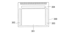
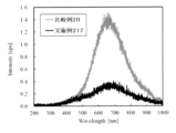
- 1 is a top view of a display device according to this embodiment; FIG. 1 is a schematic cross-sectional view of a TFT manufactured in an example; FIG. FIG. 10 is CL spectra measured in Example 217 and Comparative Example 20.
- film or “thin film” and the term “layer” can be interchanged depending on the case.
- oxide sintered body may be simply referred to as “sintered body”.
- sputtering target may be simply referred to as “target”.
- electrically connected includes the case of being connected via "something that has some electrical action”.
- something that has some kind of electrical action is not particularly limited as long as it enables transmission and reception of electrical signals between connection objects.
- things having some electrical action include electrodes, wirings, switching elements (such as transistors), resistive elements, inductors, capacitors, and other elements having various functions.
- source and drain functions of a transistor may be interchanged when using transistors with different polarities or when the direction of current changes in circuit operation. Therefore, the terms source and drain can be used interchangeably in this specification and the like.
- x to y represents a numerical range of "x or more and y or less”.
- the upper and lower limits recited for numerical ranges can be arbitrarily combined.
- the form which combined two or more of the individual forms of this invention described below is also the form of this invention.
- the crystalline oxide thin film according to this embodiment is a crystalline oxide thin film containing In as a main component.
- a low-resistance region A and a high-resistance region B having different spreading resistance values measured by a scanning spreading resistance microscope (SSRM) are provided, and the spreading resistance of the high-resistance region B is The value is eight times or more the spreading resistance value of the low resistance region A.
- the crystalline oxide thin film according to this embodiment is mainly composed of In element.
- Being the main component means that the composition ratio of In (atomic %: at %) is 50 at % or more with respect to all metal elements in the crystalline oxide thin film.
- the composition ratio of In is preferably 70 at % or more, more preferably 80 at % or more, and even more preferably 85 at % or more. If 50 at % or more of the total number of metal atoms constituting the crystalline oxide thin film is In element, sufficiently high mobility can be exhibited when the crystalline oxide thin film according to the present embodiment is employed for a TFT. .
- crystalline oxide thin films include H, B, C, N, O, F, Mg, Al, Si, O, S, Cl, Ar, Ca, Sc, Ti, V, Cr, Mn, Fe, Co, Ni, Cu, Zn, Ga, Ge, Y, Zr, Nb, Mo, Tc, Ru, Rh, Pd, Ag, Cd, Sn, Sb, Cs, Ba, Ln, Hf, Ta, W, Re, It may contain one or more elements selected from the group consisting of Os, Ir, Pt, Au, Pb and Bi.
- the crystalline oxide thin film may consist essentially of elements selected from In, Mg, Al, Si, Zn, Ga, Mo, Sn, Ln elements (lanthanoid elements) and O.
- the term “substantially” refers to the range in which the effects of the present invention due to the combination of In, Mg, Al, Si, Zn, Ga, Mo, Sn, Ln and O are produced, and This means that the crystalline oxide thin film may contain other components.
- the metal elements are In and Ga, and the atomic ratio satisfies the following formula (11). [Ga]/([In]+[Ga]) ⁇ 22at% (11)
- F or H may be included in addition to inevitable impurities and O.
- a more preferable second form of the crystalline oxide thin film includes In and B, Al, Sc, Mg, Zn, Ti, Y, Zr, Mo, Sn, Hf, W, Nb, and Ta as metal elements. , Ge, Si, La, Ce, Pr, Nd, Sm, Dy, Ho, Er, Tm, Yb and Lu.
- the ratio satisfies the following formula (12). [X]/([In]+[X]) ⁇ 15at% (12)
- F or H may be included in addition to inevitable impurities and O.
- the ratio of In increases, and the bixbite structure in which the In site is substituted with X can be crystallized even by annealing at a low temperature such as 300.degree. Furthermore, by adding the element X, which has a strong bonding force with oxygen, oxygen deficiency after annealing can be suppressed, and a film stable as a semiconductor can be formed.
- a more preferred third form of the crystalline oxide thin film includes metal elements In, Ga, B, Al, Sc, Mg, Zn, Ti, Y, Zr, Mo, Sn, Hf, W, Consists of one or more elements X selected from Nb, Ta, Ge, Si, La, Ce, Pr, Nd, Sm, Dy, Ho, Er, Tm, Yb and Lu, and metal elements other than In and Ga as additive elements
- X the atomic ratio satisfies the following formulas (13) and (14).
- a more preferred fourth form of the crystalline oxide thin film includes metal elements In, Sn, B, Al, Sc, Mg, Zn, Ti, Y, Zr, Mo, Hf, W, Nb, It consists of one or more elements X selected from Ta, Ge, Si, La, Ce, Pr, Nd, Sm, Dy, Ho, Er, Tm, Yb and Lu, and metal elements other than In and Sn are called element X , the atomic ratio satisfies the following formulas (15) and (16).
- F or H may be included in addition to inevitable impurities and O.
- the ratio of In is increased, and even with annealing at a low temperature such as 300° C., it is possible to crystallize into a bixbite structure in which the In sites are substituted with Sn. Since Sn has a large ion radius and orbital overlap with In is large, high mobility can be maintained. Further, by adding the additive element X having a strong bonding force with oxygen, the oxygen vacancies after annealing can be further suppressed, and a film stable as a semiconductor can be formed.
- a more preferable fifth form of the crystalline oxide thin film includes In, Zn, B, Al, Sc, Mg, Ti, Y, Zr, Mo, Hf, W, Nb, Ta, It consists of one or more elements X selected from Ge, Si, La, Ce, Pr, Nd, Sm, Dy, Ho, Er, Tm, Yb and Lu, and when the element X is a metal element other than In and Zn , the atomic ratio satisfies the following formulas (17) and (18).
- F or H may be included in addition to inevitable impurities and O.
- the ratio of In is increased, and the bixbite structure in which the In sites are substituted with Zn can be crystallized even by annealing at a low temperature such as 300.degree.
- Zn By adding Zn, the film immediately after the film formation can be made amorphous, and the film can be processed without residue during semiconductor patterning using acid during the fabrication of TFTs.
- an additive element X having a strong bonding force with oxygen oxygen vacancies after annealing can be suppressed, and a film stable as a semiconductor can be formed.
- the content (atomic ratio) of each metal element in the crystalline oxide thin film can be obtained by measuring the abundance of each element by ICP (Inductive Coupled Plasma) measurement or XRF (X-ray Fluorescence) measurement.
- ICP Inductive Coupled Plasma
- XRF X-ray Fluorescence
- ICP-OES inductively coupled plasma emission spectrometer
- a thin-film fluorescent X-ray analyzer AZX400, manufactured by Rigaku Corporation
- the content (atomic ratio) of each metal element in the crystalline oxide thin film was measured by TEM-EDS measurement using an electron microscope, ICP measurement using an inductively coupled plasma emission spectrometer, and sector-type dynamic secondary ion mass measurement. Analysis can be performed with an error accuracy within 2 atomic % by SIMS analysis using an analyzer.
- the metal elements in the crystal oxide thin film are identified by cross-sectional TEM-EDS, and the composition ratio is identified within an error range of about 10 atomic % by semi-quantitative analysis.
- a standard oxide thin film is prepared from 10 kinds of composition ratios with known atomic ratios of metal elements in the range of 20 atomic % from the results of semi-quantitative analysis.
- the value measured by the inductively coupled plasma emission spectrometer or the thin film fluorescence X-ray spectrometer is taken as the absolute value of the composition ratio.
- a source/drain electrode was formed with the same material as the TFT element and with the same channel length.
- the mass spectrum intensity of each element is obtained, and a calibration curve of known element concentrations and mass spectrum intensities is prepared.
- the oxide thin film portion of the actual TFT element taken out from the panel is subjected to SIMS analysis using a sector-type dynamic secondary ion mass spectrometer, and the atomic ratio is calculated from the spectral intensity using the calibration curve described above.
- the calculated atomic ratio can be confirmed with an accuracy within 2 atomic % of the atomic ratio of the oxide thin film separately measured by a thin film fluorescence X-ray spectrometer or an inductively coupled plasma emission spectrometer.
- the crystalline oxide thin film according to the present embodiment has a low resistance region A and a high resistance region B having different spreading resistance values measured by a scanning spreading resistance microscope (SSRM) in the plane direction of the crystalline oxide thin film,
- the ratio (R B /R A ) of the spreading resistance value RB of the high resistance region B to the spreading resistance value RA of the low resistance region A is 8 times or more.
- R B /R A is preferably 10 times or more, more preferably 15 times or more.
- a sufficient energy barrier is formed between the low-resistance region A and the high-resistance region B. Therefore, when a crystalline oxide thin film is used as the channel layer of a TFT, the DIBL phenomenon is suppressed.
- R B /R A is not particularly limited, it is, for example, 100,000 times or less, and may be 10,000 times or less. If RB / RA is too large, the energy barrier between the low-resistance region A and the high-resistance region B is too large, and thus becomes an electron injection barrier when a voltage Vd is applied between the source electrode and the drain electrode. , the mobility of the TFT is reduced.
- “high” and “low” of "resistance” mean the relative high and low of the spreading resistance value of the region A and the region B. As shown in FIG.
- the spreading resistance value RA of the low resistance region A is preferably 1 ⁇ or more and 1 ⁇ 10 6 ⁇ or less.
- the low-resistance region A is formed, for example, in the presence of indium-tin oxide (ITO), indium zinc oxide (IZO), aluminum, etc., by a method of heat treatment (annealing), plasma treatment, or ion implantation. can be formed by lowering the resistance of A region that is not subjected to the low-resistance treatment becomes a high-resistance region B.
- ITO indium-tin oxide
- IZO indium zinc oxide
- aluminum aluminum
- ion implantation ion implantation
- the thickness of the crystalline oxide thin film is preferably 80 nm or less.
- the thickness of the crystalline oxide thin film is preferably 60 nm or less, more preferably 50 nm or less, and particularly preferably 40 nm or less.
- the thickness of the crystalline oxide thin film is, for example, 3 nm or more, may be 5 nm or more, or may be 10 nm or more.
- the film thickness of the crystalline oxide thin film is measured based on a cross-sectional TEM observation image (sometimes referred to as a “cross-sectional TEM image”).
- the dC/dV value at the boundary between the low resistance region A and the high resistance region B is the dC/dV value of the high resistance region B Greater than value.
- the carrier concentration continuously changes at the boundary between the low-resistance region A and the high-resistance region B, and electrons are accumulated at the interface between the gate insulating film and the channel layer when the TFT is driven (here, Vg>0). There is no electrical potential barrier between the source and the drain in the state), and high mobility characteristics can be obtained. SCM measurement conditions will be described in detail in Examples.
- the average grain boundary angle ⁇ between the lower surface of the crystalline oxide thin film and the grain boundaries in the thin film is preferably 70° or more and 110° or less.
- the average grain boundary angle ⁇ between the thin film surface and the crystal grain boundaries in the thin film is measured based on a cross-sectional TEM observation image (sometimes referred to as a "cross-sectional TEM image"). That is, it is calculated by analyzing the angle formed between the crystal grain boundary and the thin film surface observed by cross-sectional TEM under magnification using a transmission electron microscope.
- the average distance D between crystal grain boundaries in the crystalline oxide thin film is preferably 0.01 ⁇ m or more and 2.0 ⁇ m or less.
- the small TFT having the crystalline oxide thin film according to the present embodiment exhibits high mobility, and uniform characteristics of mobility and threshold voltage (Vth) with respect to device shape can be obtained.
- Vth threshold voltage
- the average distance D between crystal grain boundaries in the thin film is measured based on the cross-sectional TEM observation image. Measurement conditions will be described in detail in Examples.
- the crystalline oxide thin film contains crystal grains having a bixbite structure in electron beam diffraction. Since the crystal grains of the bixbite structure are cubic crystals with good symmetry, it is possible to suppress deterioration of TFT characteristics (mobility) even across crystal grain boundaries.
- the crystal oxide thin film of the present embodiment is a crystal oxide thin film containing In as a main component, and has a thickness of 80 nm or less.
- a high carrier concentration region A and a low carrier concentration region B having different carrier concentrations are provided in the plane direction of the crystalline oxide thin film, and the carrier concentration of the high carrier concentration region A is 10 19 cm ⁇ 3 or more and 10 22 cm ⁇ 3 . 3 or less, and the carrier concentration of the high carrier concentration region A is 8 times or more the carrier concentration of the low carrier concentration region B. It is preferably 10 times or more, more preferably 15 times or more, and still more preferably 100 times or more.
- an energy barrier is formed between the low-resistance region and the high-resistance region.
- the crystalline oxide thin film is defined by a high carrier concentration region A and a low carrier concentration region B instead of the low resistance region A and the high resistance region B of the crystalline oxide thin film of the first embodiment.
- the high carrier concentration region A corresponds to the low resistance region A
- the low carrier concentration region B corresponds to the high resistance region B.
- the film thickness of the crystalline oxide thin film is 80 nm or less.
- the thickness of the crystalline oxide thin film is preferably 60 nm or less, more preferably 50 nm or less, and particularly preferably 40 nm or less.
- the thickness of the crystalline oxide thin film is, for example, 3 nm or more, may be 5 nm or more, or may be 10 nm or more.
- the carrier concentration of the high carrier concentration region A is 10 19 cm ⁇ 3 or more and 10 22 cm ⁇ 3 or less, preferably 10 19 cm ⁇ 3 or more and 10 21 cm ⁇ 3 or less.
- the carrier concentration of the low carrier concentration region B is preferably 10 15 cm ⁇ 3 or more and less than 10 19 cm ⁇ 3 .
- the constituent elements, manufacturing method, preferred range, etc. of the crystalline oxide thin film according to this embodiment are the same as those of the first embodiment.
- the crystalline oxide thin film of the first embodiment has been described, but the same applies to the second embodiment. Applicable. Specifically, by replacing the low resistance region A with the high carrier concentration region A and the high resistance region B with the low carrier concentration region B, the application example of the second embodiment is obtained.
- the crystalline oxide thin film of the present embodiment is a crystalline oxide thin film containing In as a main component, has a thickness of 80 nm or less, and has crystals of the crystalline oxide thin film.
- the average distance D between grain boundaries is 2 ⁇ m or less, and the carrier concentration is 10 19 cm ⁇ 3 or more and 10 22 cm ⁇ 3 or less.
- the crystalline oxide thin film of this embodiment has the high carrier concentration region A of the crystalline oxide thin film of the second embodiment.
- the constituent elements, manufacturing method, preferred range, etc. of the crystalline oxide thin film according to this embodiment are the same as those of the first and second embodiments.
- Laminate A laminate according to the present embodiment has the crystalline oxide thin film according to the embodiment described above and a lower layer that supports the crystalline oxide thin film.
- FIG. 1 is a schematic cross-sectional view of a laminate as an example of the present embodiment.
- the laminate 10 has a crystalline oxide thin film 11 and a lower layer 12 supporting the crystalline oxide thin film 11 .
- the crystal oxide thin film 11 has one high resistance region B (11B) and two low resistance regions A (11A) sandwiching the high resistance region B (11B) in the plane direction.
- FIG. 2 is a schematic cross-sectional view of a laminate of another example of the present embodiment.
- the stack 20 has a crystalline oxide thin film 11 and a lower layer 12 supporting the crystalline oxide thin film 11 .
- the crystalline oxide thin film 11 has high-resistance regions B (11B) and low-resistance regions A (11A) alternately formed in the plane direction.
- the lower layer 12 is a single layer, but is not limited to this, and may be a laminate of two or more layers.
- the lower layer 12 includes a substrate, a buffer layer, an insulating layer, an electrode, a light shield layer, and the like. Each of these may be composed of two or more layers.
- the average grain boundary angle ⁇ sub between the surface of the lower layer and the crystal grain boundaries in the crystalline oxide thin film is preferably 70° or more and 110° or less.
- the average grain boundary angle ⁇ sub between the surface of the lower layer and the crystal grain boundaries in the crystalline oxide thin film satisfies the above range, the crystal grain boundaries are formed with respect to the surface of the lower layer with which the crystalline oxide thin film is in contact. can exist in secret.
- an electrode for example, a source electrode
- crystal grain boundaries are densely present with respect to the electrode surface.
- the contact area with the electrode is narrow (for example, a small TFT)
- electron injection into the crystalline oxide thin film can be ensured, and a decrease in mobility can be suppressed.
- the crystalline oxide thin film of the present embodiment and the laminated body including the crystalline oxide thin film include, for example, a substrate, a buffer layer, an insulating layer, and the like, in which the lower layers constituting the TFT are composed mainly of In oxide. It can be manufactured by forming a thin film and then subjecting desired portions to the above-described resistance reduction treatment.
- the film formation method is not particularly limited, for example, DC sputtering, AC sputtering, RF sputtering, ICP sputtering, reactive sputtering, ion plating, ALD, PLD, MO-CVD, ICP-CVD, sol-gel method, coating method, mist CVD can be mentioned.
- the film may be formed using a planar sputtering cathode device or a rotary sputtering cathode device.
- a film is formed by DC sputtering using a sputtering target containing an oxide sintered body containing an oxide of In as a main component, and then a desired portion is subjected to the above-described low resistance treatment.
- the atomic composition ratio of the crystalline oxide thin film obtained by the sputtering method reflects the atomic composition ratio of the oxide sintered body in the sputtering target. Therefore, it is preferable to form a film using a sputtering target containing an oxide sintered body having an atomic composition ratio similar to that of the desired oxide thin film.
- heat treatment may be performed before the resistance reduction treatment.
- the heat treatment process is not particularly limited, but a hot air furnace, an IR furnace, a lamp annealing device, a laser annealing device, a thermal plasma device, or the like can be used.
- plasma oxidation treatment with N 2 O or plasma oxidation treatment with O 2 may be performed before the low resistance treatment.
- the apparatus for plasma oxidation treatment is not particularly limited, but PE-CVD and the like can be mentioned.
- the target used in the sputtering method preferably has an impurity metal content of 500 ppm or less, more preferably 100 ppm or less.
- the content of impurity metals in the target can be measured by ICP or SIMS as in the case of the crystalline oxide thin film.
- Impurities contained in the target are elements that are not intentionally added and are mixed in raw materials or in the manufacturing process, and are trace elements that do not substantially affect the performance of the target and semiconductor. ” means an element that is a metal element among the elements as “impurities”.
- the sputtering target may consist essentially of In and an element selected from Mg, Al, Si, Zn, Ga, Mo, Sn, Ln elements (lanthanoid elements) and O.
- the term “substantially” means that the sputtering target is within the range where the effects of the present invention due to the combination of Mg, Al, Si, Zn, Ga, Mo, Sn, Ln and O other than In are produced. , means that it may contain other ingredients.
- a more preferable first form of the sputtering target is an oxide in which the metal elements are In and Ga, and the atomic ratio is the following formula (11) meet. [Ga]/([In]+[Ga]) ⁇ 22at% (11)
- a more preferred second form of the sputtering target includes In and B, Al, Sc, Mg, Zn, Ti, Y, Zr, Mo, Sn, Hf, W, Nb, Ta, Ge, Si, La, An oxide composed of one or more elements X selected from Ce, Pr, Nd, Sm, Dy, Ho, Er, Tm, Yb, and Lu, where X is a metal element other than In, as an atomic ratio It satisfies the following formula (12). [X]/([In]+[X]) ⁇ 15at% (12)
- a more preferred third form of the sputtering target contains In, Ga, B, Al, Sc, Mg, Zn, Ti, Y, Zr, Mo, Sn, Hf, W, Nb, Ta, Ge, and Si as metal elements. , La, Ce, Pr, Nd, Sm, Dy, Ho, Er, Tm, Yb and Lu. , the atomic ratio satisfies the following formulas (13) and (14). [Ga]/([In]+[Ga]+[X]) ⁇ 22.5 at % (13) [X]/([In]+[Ga]+[X]) ⁇ 8.0at% (14)
- a more preferred fourth form of the sputtering target contains In, Sn, B, Al, Sc, Mg, Zn, Ti, Y, Zr, Mo, Hf, W, Nb, Ta, Ge, Si, and La as metal elements. , Ce, Pr, Nd, Sm, Dy, Ho, Er, Tm, Yb, and Lu, where the element X is a metal element other than In and Sn
- the atomic ratio satisfies the following formulas (15) and (16). [Sn]/([In]+[Sn]+[X]) ⁇ 20at% (15) [X]/([In]+[Sn]+[X]) ⁇ 8.0at% (16)
- a more preferred fifth form of the sputtering target contains In, Zn, B, Al, Sc, Mg, Ti, Y, Zr, Mo, Hf, W, Nb, Ta, Ge, Si, La, and Ce as metal elements. , Pr, Nd, Sm, Dy, Ho, Er, Tm, Yb and Lu.
- the atomic ratio satisfies the following formulas (17) and (18). [Zn]/([In]+[Zn]+[X]) ⁇ 12at% (17) [X]/([In]+[Zn]+[X]) ⁇ 8.0at% (18)
- An oxide thin film obtained by sputtering using a sputtering target containing indium oxide as a main component is an amorphous oxide thin film.
- This oxide thin film is patterned into islands by photolithography, and heated to crystallize before forming a protective film, thereby obtaining a crystalline oxide thin film in which surface crystals have a single crystal orientation. can. Each step will be described below.
- the above-described sputtering target is used, and one or more gases selected from the group consisting of argon and oxygen substantially free of impurity gases are used as the sputtering gas to form the oxide thin film by sputtering. to form a film.
- the sputtering target is preferably mounted in an RF magnetron sputtering device or a DC magnetron sputtering device for sputtering.
- the sputtering gas substantially does not contain impurity gases
- the gases other than the sputtering gas are excluded, excluding adsorbed water brought in when the gas is inserted, and gases that cannot be eliminated (inevitable impurity gases) such as chamber leaks and adsorbed gases.
- the impurity gas is not actively introduced. Impurities are preferably excluded from the gas (sputtering gas) introduced during sputtering film formation, if possible.
- the impurity gas content in the sputtering gas is preferably 0.1% by volume or less, more preferably 0.05% by volume or less. If the proportion of the impurity gas is 0.1% by volume or less, crystallization of the oxide thin film proceeds without problems.
- the purity of high-purity argon and high-purity oxygen, which are examples of the sputtering gas, is preferably 99% by volume or higher, more preferably 99.9% by volume or higher, and even more preferably 99.99% by volume or higher.
- the gas (sputtering gas) to be introduced during sputtering film formation is not particularly limited, but examples thereof include argon, nitrogen, oxygen, water, hydrogen, and a mixed gas containing two or more of these gases.
- the oxygen partial pressure in the mixed gas is preferably more than 0% by volume and 50% by volume or less, more preferably more than 0% by volume and 20% by volume or less. . If the oxygen partial pressure is more than 0% by volume and 50% by volume or less, the material is easily crystallized into a semiconductor when heated. By changing the oxygen partial pressure, the degree of oxidation of the oxide thin film, that is, the degree of crystallization can be adjusted.
- the oxygen partial pressure may be appropriately selected as required.
- the water pressure in the mixed gas is preferably more than 0.03% by volume and 10% by volume or less, and more than 0.03% by volume and 5% by volume or less. more preferred.
- the water pressure is more than 0.03% by volume and 5% by volume or less, the material is easily crystallized to become a semiconductor when heated.
- a mixed gas of hydrogen and oxygen may be used instead of water.
- the crystalline oxide thin film according to the present embodiment preferably contains In element as a main component.
- This oxide thin film By heating this oxide thin film in a heat treatment step to be described later, columnar crystals can be grown on the lower layer.
- the oxide thin film formed as described above By applying the oxide thin film formed as described above to a small TFT, the electron carrier injection property is excellent during driving, resulting in high mobility, and the device shape of mobility and threshold voltage (Vth). uniform characteristics for
- Step of Forming TFT Constituent Layers When forming TFT constituent layers such as an insulating layer on the crystalline oxide thin film, it is preferable to form the constituent layers on the oxide thin film after heat-treating the obtained oxide thin film. . By performing annealing before forming the constituent layers of the TFT, oxygen and hydrogen are diffused at the time of annealing, and high-quality columnar crystals are obtained. A TFT is obtained.
- Heat treatment process After forming the oxide thin film, a heat treatment is performed. This heat treatment is sometimes called annealing.
- the heat treatment temperature is preferably 250° C. or higher and 500° C. or lower, more preferably 280° C. or higher and 470° C. or lower, and even more preferably 300° C. or higher and 450° C. or lower. If the heat treatment temperature after forming the oxide thin film is 250° C. or higher, the oxide thin film is easily crystallized. If the heat treatment temperature after forming the oxide thin film is 500° C. or less, it is possible to prevent abnormal growth of crystals and increase the size of the crystal grains, and control the crystal grain size to be small.
- the heating time in the heat treatment step is preferably 0.1 hours or more and 5 hours or less, more preferably 0.3 hours or more and 3 hours or less, and 0.5 hours or more and 2 hours or less. is more preferred. If the heating time in the heat treatment step is 0.1 hour or longer, the oxide thin film is easily crystallized without crystallization. If the heating time in the heat treatment step is 5 hours or less, it is economical.
- the term "heating time” refers to the time (holding time) during which a predetermined maximum temperature is maintained during heat treatment.
- the heating rate in the heat treatment step is preferably 2° C./min or more and 40° C./min or less, and more preferably 3° C./min or more and 20° C./min or less. If the heating rate in the heat treatment step is 2° C./min or more, the production efficiency of the oxide thin film is improved as compared with the case of less than 1° C./min. If the heating rate in the heat treatment step is 40° C./min or less, the metal elements are uniformly diffused during crystallization, and crystals in which the metal is not segregated at grain boundaries can be formed. Also, the heating rate in the heat treatment process is a value obtained by dividing the actual temperature of the oxide thin film by time, unlike the value calculated from the set temperature and set time of the furnace. The actual temperature of the oxide thin film can be determined, for example, by measuring an area within 1 cm of the oxide thin film in the furnace with a thermocouple.
- the heat treatment process is performed in an air atmosphere with a humidity of 10% or more at 25°C.
- the heat treatment step is performed in the atmosphere with a humidity of 10% or more, hydrogen and oxygen diffuse into the film during annealing, and crystallization can be promoted.
- the heat treatment process is preferably performed after patterning the oxide thin film.
- crystallization can be promoted while excess oxygen present in the film during film formation and organic matter adhering during patterning are eliminated.
- Crystal defects in the film after heat treatment can be evaluated by defect analysis such as cathodoluminescence (CL).
- CL cathodoluminescence
- the heat treatment process may be performed multiple times. For example, after patterning the oxide thin film, the heat treatment step (first heat treatment step) described above may be performed, and after manufacturing the TFT element, the heat treatment step (second heat treatment step) may be performed as the final step.
- the second heat treatment step is preferably performed at a higher annealing temperature than the first heat treatment step.
- a low resistance region A and a high resistance region B are formed in the crystalline oxide thin film obtained in the heat treatment step.
- the low-resistance region A is not particularly limited, but for example, in the presence of indium tin oxide (ITO), aluminum, etc., a method of heat treatment (annealing), a plasma treatment, a dry process such as ion implantation, etc. It can be formed by lowering the resistance of the part.
- a region that is not subjected to the low-resistance treatment becomes a high-resistance region B.
- an ITO layer is formed by sputtering or the like on the crystal oxide thin film in the region where the resistance is to be reduced, and then heated to 250° C. or higher and 500° C. or lower (annealing may be performed at a temperature of preferably 280° C. or more and 470° C. or less, more preferably 300° C. or more and 450° C. or less for a time of 0.1 hour or more and 5 hours or less. After annealing, the ITO layer may be etched away or left in place.
- an aluminum layer is formed by sputtering or the like on the crystal oxide thin film in the region where the resistance is to be reduced, and then heated to 250° C. or more and 500° C. or less (annealing may be performed at a temperature of preferably 280° C. or more and 470° C. or less, more preferably 300° C. or more and 450° C. or less for a time of 0.1 hour or more and 5 hours or less. After annealing, it may remain as aluminum or become aluminum oxide. In either case, the aluminum or aluminum oxide layer may be removed by etching or may be left as it is.
- the crystalline oxide thin film obtained in the heat treatment step is treated.
- Gases used for plasma processing are not particularly limited, but examples include H 2 , He, Ar, N 2 , F-based gases, and the like.
- Elements used for plasma treatment are generally preferably elements with small ionic radii. By performing plasma treatment using these elements, oxygen vacancies are generated in the crystalline oxide thin film, the carrier concentration is increased, and the resistance is lowered.
- ions may be implanted through the Ions used for implantation are not particularly limited, but examples include H + , He + , B + , N + , F + , PHx + , and Ar + . Any element that generates oxygen vacancies by ion implantation or an element that emits electrons and acts as a donor when left in the film may be used. Also, the element may or may not remain in the film.
- the low-resistance treatment step is preferably performed after forming the gate insulating film and/or the gate electrode.
- the low resistance region A and the high resistance region B can be formed using a gate insulating film and/or a gate electrode instead of a mask (self-alignment).
- the region where the ITO layer is directly laminated in the crystalline oxide thin film becomes the low resistance region A, and the region under the gate insulating film and/or the gate electrode becomes the high resistance region B. Become.
- a TFT according to this embodiment includes the crystalline oxide thin film or laminate of the present invention described above.
- the crystalline oxide thin film of the present invention is used as a channel layer of a TFT. More preferably, both ends of the channel layer, that is, the vicinity of the regions where the source and drain electrodes are connected are the low-resistance regions A of the crystalline oxide thin film, and the region in contact with the lower surface of the gate insulating film is the high-resistance region. B is preferred.
- a TFT has a channel layer, a source electrode and a drain electrode respectively connected to both ends of the channel layer, and a gate electrode stacked on the channel layer via a gate insulating film
- the channel layer is a crystalline oxide thin film, and has a structure in which a gate insulating film is formed in a high resistance region B and a source electrode and a drain electrode are formed in a low resistance region A.
- the distance L off from the end of the source electrode and the end of the drain electrode to the intersection of the perpendicular line drawn in the thickness direction from the end of the gate electrode and the crystalline oxide thin film is 4 ⁇ m or more and 20 ⁇ m or less.
- the average distance D between crystal grain boundaries of the crystalline oxide thin film and the distance Loff satisfy the following formula (1). 2 ⁇ L off /D ⁇ 100 (1)
- the TFT has a contact region length Ls between the source and drain electrodes and the channel layer of 4 ⁇ m or more and 20 ⁇ m or less.
- the average distance D between crystal grain boundaries of the crystalline oxide thin film and the contact region length Ls satisfy the following formula (2). 1 ⁇ Ls/D ⁇ 100 (2) As a result, excellent mobility is exhibited even if the contact regions between the source and drain electrodes and the channel layer are small.
- TFTs manufactured in the prior art use a crystalline oxide thin film in order to obtain high mobility.
- the length of the contact region between the source electrode and the oxide thin film was about 100 ⁇ m. Therefore, even if the crystal grain size of the oxide thin film is 1 ⁇ m or more, about 100 crystal grain boundaries are present in the contact region with the source electrode, and the crystal grain boundaries that are conductive regions with respect to the source electrode are present. A sufficient number were in contact with each other, and there was no major problem from the viewpoint of mobility.
- the conventional technology has a structure in which parasitic capacitance is generated in the region where the gate electrode and the source and drain electrodes overlap. Therefore, it was not a big problem.
- displays such as OLEDs are required to have high resolution, high-speed driving, and large area.
- the size of TFTs is becoming smaller. Therefore, it is necessary to control the characteristics of small TFTs patterned by photolithography, instead of film formation using a metal mask as in the conventional art.
- parasitic capacitance is reduced in order to eliminate the RC delay that delays the time from input to driving due to the effects of parasitic resistance and parasitic capacitance in the backplane drive circuit.
- it is necessary to reduce variations in parasitic capacitance as much as possible in order to eliminate luminance unevenness in each pixel of the OLED.
- the gate electrode is used as a mask to selectively lower the resistance of the semiconductor, and the regions are used as the source and drain regions.
- the oxide thin film is applied to a self-aligned small TFT structure (self-aligned small TFT structure)
- the length of the contact region between the source electrode and the crystalline oxide thin film is shortened.
- the intersection of the perpendicular drawn from the edge of the gate electrode in the thickness direction and the crystalline oxide thin film becomes shorter from the edge of the source electrode and the edge of the drain electrode.
- the edges of the source electrode and the drain electrode A sufficient number of crystal grain boundaries exist in the region from the edge to the intersection of the perpendicular line drawn in the thickness direction from the edge of the gate electrode and the crystal oxide thin film, and in the contact region with the source electrode. A sufficient number of grain boundaries must be present. According to the TFT according to the present embodiment, since the distance L off , the contact region length Ls, the formulas (1) and (2) are satisfied, the mobility is excellent and the Vth can be stably controlled.
- the horizontal gap ⁇ L between the low resistance region A and the gate electrode is less than 1 ⁇ m. Since the crystalline oxide thin film of the present invention is suitable for self-aligned TFTs, the gap ⁇ L can be made extremely small.
- the TFT according to this embodiment can be manufactured by adopting the above-described method for manufacturing the crystalline oxide thin film and laminate. That is, a sputtering target is used, and one or more gases selected from the group consisting of argon, nitrogen, hydrogen, water, and oxygen substantially free of impurity gases are used as the sputtering gas to form an oxide thin film by sputtering.
- This manufacturing method includes a step of forming a film (sometimes referred to as a film forming step) and a step of heat-treating the oxide thin film (sometimes referred to as a heat-treating step). Each condition of the film forming process and the heat treatment process is as described above.
- the source electrode, drain electrode, gate electrode and gate insulating film can be formed using known materials and forming methods.
- a crystalline oxide thin film according to one embodiment has a high mobility in a direction parallel to the film surface.
- a crystalline oxide thin film for the oxide semiconductor layer (channel layer) or conductive region of a small self-aligned TFT, high mobility and stable control of Vth can be achieved.
- a transfer characteristic Id-Vg graph is created when each Vd is applied, the transconductance (Gm) of each Vg is calculated, and the mobility is obtained using the linear region or saturation region equation.
- Current Id is the current between the source and drain electrodes
- voltage Vd is the voltage applied between the source and drain electrodes (drain voltage)
- voltage Vg is the voltage applied between the source and gate electrodes. (gate voltage).
- the mobility is 20 cm 2 /(V ⁇ s) or more, and the higher the mobility, the better.
- an ohmic electrode such as metal, ITO, or IZO is arranged on one surface of the high resistance region B, and the other surface has a work function of 4.8 eV or more.
- Schottky barrier diodes, MES-FETs, etc. can be configured by arranging Schottky electrodes of oxide or the like.
- the shape of the thin film transistor according to the present embodiment is not particularly limited as long as it is self-aligned, but a top gate type transistor, a back channel etch type transistor, an etch stopper type transistor, or the like is preferable.
- FIG. 3A is a schematic cross-sectional view of an example of the TFT of this embodiment.
- the TFT 50 is a top-gate type TFT, and includes a substrate 21, a buffer layer 22, a channel layer (a crystalline oxide thin film) 11, an ITO layer 23, a gate insulating film 24, a gate electrode 25, an interlayer insulating film 26, a source electrode 27, It has a drain electrode 28 and a protective film 29 .
- the TFT 50 has a structure in which a substrate 21, a buffer layer 22, and a channel layer (crystalline oxide thin film) 11 are laminated in this order.
- a high resistance region 11B is provided in the central portion of the channel layer 11, and a gate insulating film 24 and a gate electrode 25 are laminated in this order on the high resistance region 11B.
- the gate insulating film 24 is an insulating film that interrupts conduction between the gate electrode 25 and the crystalline oxide thin film 11 .
- Low resistance regions 11A-1 and 11A-2 of the channel layer 11 are present on both sides of the high resistance region 11B.
- the low resistance regions 11A-1 and 11A-2 and the gate electrode 25 are covered with an ITO layer 23 and an interlayer insulating film 26. As shown in FIG.
- the ITO layer 23 is used when forming the low resistance region of the channel layer 11 .
- a source electrode 27 and a drain electrode 28 are connected to the low resistance regions 11A-1 and 11A-2, respectively, through contact holes provided in the ITO layer 23 and the interlayer insulating film 26 .
- the source electrode 27 and the drain electrode 28 are conductive terminals for allowing source current and drain current to flow through the channel layer 11 .
- a protective film 29 is provided so as to cover the TFT constituent layers such as the interlayer insulating film 26, the source electrode 27, the drain electrode 28, and the like.
- FIG. 3B is an enlarged view of the vicinity of the source electrode in FIG. 3A.
- FIG. 3B shows the distance L off from the edge of the source electrode and the edge of the drain electrode to the intersection of the perpendicular line drawn in the thickness direction from the edge of the gate electrode and the crystalline oxide thin film in the TFT 50 , the source electrode
- the contact region length Ls between (the drain electrode) and the channel layer and the horizontal gap ⁇ L between the low resistance region A and the gate electrode are illustrated.
- FIG. 4 is a schematic cross-sectional view of another example of the TFT of this embodiment.
- the TFT 51 has the same configuration as the TFT 50 except that the write shield layer 31 is provided between the substrate 21 and the buffer layer 22 .
- the light shield layer 31 is formed to suppress malfunction of the TFT due to light.
- FIG. 5 is a schematic cross-sectional view of another example of the TFT of this embodiment.
- the TFT 52 has the same configuration as the TFT 50 except that the ITO layer 23 is not formed.
- the low resistance regions 11A-1 and 11A-2 are formed by, for example, an ion implantation method or a dry process such as plasma processing.
- FIG. 6 is a schematic cross-sectional view of another example of the TFT of this embodiment.
- the TFT 60 has the same configuration as the TFT 50 except that the ITO layer 23 is not formed and the interlayer insulating film 26 has a two-layer structure (interlayer insulating films 26-1 and 26-2).
- the region under the gate electrode 25 of the interlayer insulating film 26-1 corresponds to the gate insulating film 24.
- the low resistance regions 11A-1 and 11A-2 are formed by ion implantation, for example.
- FIG. 7 is a schematic cross-sectional view of another example of the TFT of this embodiment.
- the TFT 70 is a bottom-gate type TFT, and includes a substrate 21, a gate electrode 25, a gate insulating film 24, a channel layer (a crystalline oxide thin film) 11, an interlayer insulating film 26, a source electrode 27, a drain electrode 28, and a protective film 29. have.
- the gate electrode 25 is formed on the substrate 21 and the gate insulating film 24 is laminated on the substrate 21 and the gate electrode 25 .
- a channel layer (crystalline oxide thin film) 11 is laminated on the gate insulating film 24, a region corresponding to the gate electrode 25 is a high resistance region 11B, and low resistance regions of the channel layer 11 are formed on both sides of the high resistance region 11B.
- the channel layer (crystalline oxide thin film) 11 is covered with an interlayer insulating film 26 .
- a source electrode 27 and a drain electrode 28 are connected to the low-resistance regions 11A-1 and 11A-2, respectively, through contact holes provided in the interlayer insulating film 26 .
- a protective film 29 is provided so as to cover the TFT constituent layers such as the interlayer insulating film 26 , the source electrode 27 and the drain electrode 28 .
- the TFT of this embodiment can be improved with a known configuration.
- any commonly used material can be selected.
- a glass substrate, a ceramic substrate, a quartz substrate, or a sapphire substrate can be used. It is also possible to apply a single crystal semiconductor substrate such as silicon or silicon carbide, a polycrystalline semiconductor substrate, a compound semiconductor substrate such as silicon germanium, an SIO (Silicon In Insulator) substrate, or the like. You may use the thing provided with the element as a board
- a flexible substrate may also be used as the substrate.
- the method of providing a TFT on a flexible substrate in addition to the method of directly fabricating a TFT on a flexible substrate, after fabricating a TFT on a non-flexible substrate, the TFT is peeled off to form a flexible substrate. There is also a method of setting it on the board. In that case, a release layer may be provided between the non-flexible substrate and the TFT.
- the material for forming the buffer layer 22 is not particularly limited, and generally used materials can be arbitrarily selected, and a laminated film can be used.
- the buffer layer 22 can be appropriately designed according to the type of substrate.
- the write shield layer 31 may be connected to the source electrode 27 or may be connected to the gate electrode 25 .
- the material for forming the write shield layer is not particularly limited, and any commonly used material can be selected. Specifically, metal electrodes such as Al, Ag, Cu, Cr, Ni, Co, Mo, Au, Ti, Zr, Ru, Y, Nb, Ta, W, and metals made of alloys containing two or more of these metals An electrode etc. are mentioned. A laminated electrode having two or more layers can also be used.
- a second buffer layer may be provided between the write shield layer 31 and the substrate 21 .
- the material for forming the second buffer layer is not particularly limited, and generally used materials can be arbitrarily selected, and a laminated film can be used.
- Materials for forming the gate insulating film are not particularly limited, and generally used materials can be arbitrarily selected, and a laminated film can be used.
- the crystalline oxide thin film as the channel layer for the source electrode and the drain electrode has a channel length (L length) of 1 ⁇ m or more and 50 ⁇ m or less.
- the channel width is not particularly limited, for example, the channel width (W length) is 1 ⁇ m or more and 1000 ⁇ m or less.
- Materials for forming the drain electrode, the source electrode and the gate electrode are not particularly limited, and commonly used materials can be arbitrarily selected. Specifically, transparent electrodes such as ITO, IZO, ZnO, SnO2 , metals such as Al, Ag, Cu, Cr, Ni, Co, Mo, Au, Ti, Zr, Ru, Y, Nb, Ta, W Electrodes, metal electrodes made of alloys containing two or more of these metals, and the like. A laminated electrode having two or more layers can also be used.
- each interlayer insulating film Materials for forming each interlayer insulating film are not particularly limited, and generally used materials can be arbitrarily selected, and laminated films can be used.
- the drain electrode, the source electrode and the conductive region regardless of the structure of the TFT. Furthermore, in the case of the bottom gate type, it is preferable to provide a protective film on the channel layer. By providing the protective film, the durability can be easily improved even when the TFT is driven for a long time.
- TEOS Tetraethoxysilane
- SiH 4 silane
- the protective film or the insulating film when forming by PE-CVD, it may be a high-temperature process.
- the protective film or the insulating film often contains impurity gas immediately after being formed, it is preferable to perform heat treatment (annealing treatment).
- annealing treatment By removing the impurity gas by heat treatment, a stable protective film or insulating film can be obtained, making it easier to form a highly durable TFT.
- annealing after forming the gate insulating film hydrogen contained in the gate insulating film diffuses to the oxide thin film, and crystal defects present on the surface of the oxide thin film are terminated with hydroxyl groups, resulting in fewer electron traps. Oxide thin films with good conductive properties can be formed.
- the crystalline oxide thin film of the present invention By using the crystalline oxide thin film of the present invention, the effect of the temperature in the PE-CVD process and the effect of the subsequent heat treatment are reduced, so even if a protective film or an insulating film is formed, the TFT characteristics stability can be improved.
- the threshold voltage (Vth) is preferably -3.0 V or more and 3.0 V or less, more preferably -2.0 V or more and 2.0 V or less, and even more preferably -1.0 V or more and 1.0 V or less. If the threshold voltage (Vth) is ⁇ 3.0 V or more and 3.0 V or less, it is possible to correct Vth to 0 V by mounting a Vth correction circuit on the TFT. When the TFT thus obtained is mounted on a panel, it is possible to drive the display without unevenness in brightness and burn-in.
- the on-off ratio is preferably 10 6 or more and 10 12 or less, more preferably 10 7 or more and 10 11 or less, and even more preferably 10 8 or more and 10 10 or less.
- a liquid crystal display can be driven when the on-off ratio is 10 6 or more.
- the on-off ratio is 10 12 or less, it is possible to drive an organic EL device with high contrast.
- the off current can be 10 ⁇ 12 A or less, and when used for the transfer transistor or reset transistor of a CMOS image sensor, the image retention time can be lengthened and the sensitivity can be improved. You can improve it.
- the OFF current value is preferably 10 ⁇ 10 A or less, more preferably 10 ⁇ 11 A or less, and even more preferably 10 ⁇ 12 A or less.
- an organic EL with high contrast can be driven.
- it is used as a transfer transistor or a reset transistor of a CMOS image sensor it is possible to lengthen the image holding time and improve the sensitivity.
- the TFT according to the present embodiment can be suitably used in electronic devices such as display elements such as solar cells, liquid crystal elements, organic electroluminescence elements and inorganic electroluminescence elements, power semiconductor elements, and touch panels.
- display elements such as solar cells, liquid crystal elements, organic electroluminescence elements and inorganic electroluminescence elements, power semiconductor elements, and touch panels.
- the thin film transistor according to the present embodiment can also be applied to various integrated circuits such as field effect transistors, logic circuits, memory circuits, and differential amplifier circuits, and can be applied to electronic devices and the like. Furthermore, the thin film transistor according to the present embodiment can be applied not only to field effect transistors but also to electrostatic induction transistors and Schottky barrier transistors.
- the thin film transistor according to this embodiment can be suitably used for a display device such as a portable display device or an in-vehicle display device, a solid-state imaging device, and the like.
- the thin film transistor according to the present embodiment can also be suitably used as a transistor for a flat panel detector for an X-ray image sensor for medical use.
- the crystalline oxide thin film according to this embodiment can also be applied to Schottky diodes, resistance change memories, and resistance elements. A case where the thin film transistor according to this embodiment is used in a display device will be described below.
- FIG. 8A is an example of a circuit diagram of a pixel portion when a liquid crystal element is applied. When this is used for a Mini LED display, FIG. 8A can be used not only for the liquid crystal control circuit but also for the LED chip control circuit.
- FIG. 8B is an example of a circuit diagram of a pixel portion when an organic EL element is applied.
- the circuit of the pixel section can be applied to a configuration in which one pixel has a plurality of pixel electrodes. Each pixel electrode is connected to a different transistor, and each transistor is configured to be driven by a different gate signal. As a result, the signals applied to the individual pixel electrodes of the pixels designed for multi-domains can be independently controlled.
- At least one of the transistors in the circuit diagram may be the TFT according to this embodiment.
- the circuit diagram is not limited to the configurations shown in FIGS. 8A and 8B.
- switches, resistive elements, capacitive elements, transistors, sensors, or logic circuits may be added.
- both the Si-based transistor and the TFT according to this embodiment may be mounted.
- FIG. 8C is a top view of the display device according to this embodiment.
- the thin film transistor according to this embodiment can be used as the transistor arranged in the pixel portion. Since the thin film transistor according to this embodiment can easily be of n-channel type, a part of a driver circuit that can be configured with n-channel type transistors is formed on the same substrate as the transistors in the pixel portion. By using the thin film transistor described in this embodiment mode for the pixel portion and the driver circuit, a highly reliable display device can be provided.
- FIG. 8C An example of a top view of an active matrix display device is shown in FIG. 8C.
- a pixel portion 301, a first scanning line driver circuit 302, a second scanning line driver circuit 303, and a signal line driver circuit 304 are formed over a substrate 300 of the display device.
- a plurality of signal lines are arranged extending from a signal line driver circuit 304
- a plurality of scanning lines are extended from a first scanning line driver circuit 302 and a second scanning line driver circuit 303 .
- Pixels each having a display element are provided in a matrix at intersection regions of the scanning lines and the signal lines.
- the substrate 300 of the display device is connected to a timing control circuit (also called a controller or control IC) via a connecting portion such as an FPC (Flexible Printed Circuit).
- a timing control circuit also called a controller or control IC
- FPC Flexible Printed Circuit
- the first scanning line driving circuit 302, the second scanning line driving circuit 303, and the signal line driving circuit 304 are formed on the same substrate 300 as the pixel portion 301.
- the number of parts such as a driving circuit provided outside is reduced, so that the cost can be reduced.
- the drive circuit is provided outside the substrate 300, it becomes necessary to extend the wiring, and the number of connections between the wirings increases.
- the number of connections between wirings can be reduced, and reliability or yield can be improved.
- Example 1 A thin film transistor (TFT) 53 shown in FIG. 9 was manufactured by the following steps. Note that the TFT 53 has the same configuration as the TFT 50 shown in FIG. 3A except that the protective layer 29 is not provided.
- Substrate temperature 25°C Ultimate pressure: 8.5 ⁇ 10 ⁇ 5 Pa
- Atmospheric gas Ar Sputtering pressure (total pressure): 0.4 Pa
- Input voltage RF300W Distance between S (substrate) and T (target): 70mm
- the oxide thin film was patterned into an island shape by photolithography to form the channel layer 11 .
- a photoresist film was formed on the oxide thin film.
- AZ1500 manufactured by AZ Electronic Materials
- Exposure was performed through a photomask having a pattern of (10+L off ⁇ 2+Ls ⁇ 2+2 (both ends) ⁇ 2) ⁇ m ⁇ 20 ⁇ m in length. After exposure, it was developed with tetramethylammonium hydroxide (TMAH). After development, the oxide thin film was etched with oxalic acid (Kanto Kagaku ITO-06N).
- the photoresist was removed to obtain a substrate 21 with a patterned oxide thin film (channel layer 11).
- the dimensions of the obtained channel layer 11 were horizontal (10+L off ⁇ 2+Ls ⁇ 2+2 (both ends) ⁇ 2) ⁇ m ⁇ vertical 20 ⁇ m.
- the substrate 21 with the channel layer 11 formed thereon was placed in a furnace, heated to 350° C. at a rate of 10° C./min in the air, and held for 1 hour. After holding the inside of the furnace at 350° C. for 1 hour, it was allowed to cool naturally, and after the temperature inside the furnace returned to room temperature, the substrate 21 was taken out from the furnace.
- Gate Insulating Film 24 a 10 nm-thick SiOx layer (gate insulating film 24) was formed by sputtering using a SiO 2 sputtering target.
- Sputtering conditions are as follows. Substrate temperature: 25°C Ultimate pressure: 8.5 ⁇ 10 ⁇ 5 Pa Atmosphere gas: mixed gas of Ar + O 2 (O 2 flow rate 30%) Sputtering pressure (total pressure): 0.4 Pa Input voltage: RF100W Distance between S (substrate) and T (target): 70 mm
- the substrate 21 was placed in a furnace, heated to 400° C. at a rate of 10° C./min in the atmosphere, and held for 1 hour. After holding the inside of the furnace at 400° C. for 1 hour, it was naturally cooled. After the temperature inside the furnace returned to room temperature, the substrate 21 was taken out from the furnace.
- a SiOx layer (gate insulating film 24) having a thickness of 100 nm was formed by sputtering using a SiO 2 sputtering target.
- Sputtering conditions are as follows. Substrate temperature: 25°C Ultimate pressure: 8.5 ⁇ 10 ⁇ 5 Pa Atmosphere gas: mixed gas of Ar + O 2 (O 2 flow rate 30%) Sputtering pressure (total pressure): 0.4 Pa Input voltage: RF100W Distance between S (substrate) and T (target): 70 mm As a result, the total thickness of the gate insulating film 24 was 110 nm.
- the gate insulating film 24 was etched with buffered hydrofluoric acid (BHF) and patterned into an island shape. Next, after removing the photoresist, using oxalic acid (Kanto Kagaku ITO-06N), the region where the channel layer 11 is exposed was etched by a film thickness of 10 nm and washed. The dimensions of the obtained gate electrode layer 25 and gate insulating film 24 were 10 ⁇ m wide ⁇ 28 ⁇ m long.
- FIG. 9 Low Resistance Processing Low resistance regions A (11A-1, 11A-2) were formed in the channel layer 11 by self-alignment using the gate electrode 25.
- FIG. An ITO sputtering target was used to form an ITO layer 23 with a thickness of 2 nm. Sputtering conditions are as follows. Substrate temperature: 25°C Ultimate pressure: 8.5 ⁇ 10 ⁇ 5 Pa Atmosphere gas: mixed gas of Ar + O 2 (O 2 flow rate 2%) Sputtering pressure (total pressure): 0.4 Pa Input voltage: DC100W Distance between S (substrate) and T (target): 70 mm
- the substrate 21 was placed in a furnace, heated to 350° C. at 10° C./min in the atmosphere, held for 1 hour, and annealed. After holding the inside of the furnace at 350° C. for 1 hour, it was allowed to cool naturally. After the temperature inside the furnace returned to room temperature, the substrate 21 was taken out from the furnace.
- Interlayer Insulating Film 26 a SiOx layer (interlayer insulating film 26) having a thickness of 150 nm was formed by sputtering using a SiO 2 sputtering target.
- Sputtering conditions are as follows. Substrate temperature: 25°C Ultimate pressure: 8.5 ⁇ 10 ⁇ 5 Pa Atmosphere gas: mixed gas of Ar + O 2 (O 2 flow rate 30%) Sputtering pressure (total pressure): 0.4 Pa Input voltage: RF100W Distance between S (substrate) and T (target): 70 mm
- Source Electrode 27 and Drain Electrode 28 were patterned by a lift-off process.
- the image reversal resist AZ5214 was exposed through a photomask formed so as to be patterned into the final device shape shown in Table 1. After the reversal baking step, the entire surface was exposed and developed with TMAH. A Mo layer having a thickness of 150 nm was formed on the patterned substrate with resist under the following sputtering conditions.
- Substrate temperature 25°C Ultimate pressure: 8.5 ⁇ 10 ⁇ 5 Pa
- Atmospheric gas Ar Sputtering pressure (total pressure): 0.4 Pa
- Input voltage DC100W Distance between S (substrate) and T (target): 70 mm
- Comparative example 1 A TFT was fabricated in the same manner as in Example 1, except that (9) resistance reduction treatment of Example 1 was not performed.
- Comparative example 2 A TFT was fabricated in the same manner as in Example 1, except that the ITO layer 23 was formed and the annealing was not performed in the (9) resistance reduction treatment of Example 1.
- Example 2 A TFT was fabricated in the same manner as in Example 1, except that in (2) formation of the oxide thin film of Example 1, an oxide sputtering target obtained from a raw material mixture having a charged composition ratio shown in Table 1 was used. In the following examples and comparative examples, a 100 nm-thick gate insulating film was formed in step (5) without forming the gate insulating film in step (7) of Example 1.
- Example 3 In the formation of the oxide thin film (2) in Example 1, the oxide sputtering target obtained from the raw material mixture having the charging composition ratio shown in Table 3 was used, the atmosphere gas was a mixed gas of Ar + O 2 during the film formation, and A TFT was fabricated in the same manner as in Example 1, except that the conditions for forming each constituent layer were changed as shown in Tables 3 and 4. Tables 3 and 4 summarize the TFT fabrication conditions.
- Comparative Examples 3-5 A TFT was fabricated in the same manner as in Example 3, except that the film thickness of the oxide thin film of Example 3 was changed as shown in Table 3, and (9) the resistance reduction treatment was changed as shown in Table 4. .
- Example 4 Comparative Examples 6-9
- the oxide sputtering target obtained from the raw material mixture having the charged composition ratio shown in Table 5 was used, and the formation conditions of each constituent layer are shown in Tables 5 and 6.
- a TFT was fabricated in the same manner as in Example 1, except for the changes shown. Tables 5 and 6 summarize the TFT fabrication conditions.
- an FIB (“FB2100 type” manufactured by Hitachi High-Technologies Corporation) apparatus was used to introduce an ion beam in the direction perpendicular to the surface of the channel layer, and a test piece of 16 ⁇ m ⁇ 4 ⁇ m was sampled. After that, for the sampled test piece, 2 in a 3 ⁇ m region from the end of the region where the source electrode or drain electrode and the channel layer overlap in the channel length direction (horizontal direction of the drawing) toward the non-overlapping region. A sample was extracted.
- FIB FIB
- the two extracted samples were subjected to Ar ion milling in the channel width direction (the depth direction in the drawing) perpendicular to the channel length direction and the film thickness direction until the thickness of the flakes reached about 100 nm, and the samples were extracted. Two samples were reduced in thickness.
- Ar ion milling ("Model 691” manufactured by Gatan) at an ion gun voltage of 4 keV until crystal grains could be confirmed.
- the cross-sectional TEM image was observed using a transmission electron microscope (“JEM-2800” manufactured by JEOL Ltd.) at an acceleration voltage of 200 kV and an observation magnification of 100,000 times (an area of about 4 ⁇ m square).
- the average grain boundary angle ⁇ with respect to the thin film surface when observing the cross section of the channel layer can be calculated by analyzing the angle formed between the crystal grain boundary observed by cross-sectional TEM and the thin film surface.
- the crystalline oxide film of each area of Ls, L off , and L is included in the channel length direction of the TFT. 3 arbitrary fields of view were extracted and observed.
- the observation points should not overlap in the channel length direction so that the entire channel layer in the TFT can be observed within a range of 4 ⁇ m square in the channel length direction ⁇ thickness direction.
- Multiple fields of view were extracted and cross-sectional TEM images were observed.
- the angle formed by the thin film surface and the crystal grain boundary was calculated by performing image analysis on the obtained cross-sectional TEM image of each field of view using "SPIP, Version 4.3.2.0" manufactured by Image Metrology. . Details are as follows.
- the cross-sectional TEM image lines of color codes H0, S0, and V10 are drawn at the crystal grain boundaries in the observed image of the crystalline oxide thin film.
- the contrast was quantified using image analysis software, and the height of (maximum density - minimum density) x 1/4 was set as the threshold.
- the grain boundary was defined as a region showing a contrast below the threshold, and the angle between the surface of each thin film and the grain boundary was obtained.
- the total value of the angles formed by each obtained thin film surface and the crystal grain boundary was divided by the number of particles, and the average value of the angles obtained in each of the obtained fields of view was taken as the average grain boundary angle ⁇ with respect to the thin film surface. .
- the average distance D when observing the cross section of the oxide thin film can be calculated by analyzing the distance between crystal grains observed by cross-sectional TEM.
- any 3 layers are selected so that the crystalline oxide film of each area of Ls, L off , and L is included in the channel length direction of the TFT.
- the average distance D between grain boundaries was calculated by performing image analysis on the obtained cross-sectional TEM images of each field of view using "SPIP, Version 4.3.2.0" manufactured by Image Metrology. Details are as follows. Lines of color codes H0, S0, and V10 are drawn on the grain boundaries of the cross-sectional TEM image. Further, the contrast was quantified using image analysis software, and the height of (maximum density - minimum density) x 1/4 was set as the threshold. Next, a region exhibiting a contrast equal to or lower than the threshold value was defined as a grain boundary, and the distance between each grain boundary and the closest grain was obtained and used as the grain boundary distance. The total value of the obtained grain boundary spacing is divided by the number of locations where the spacing is measured, and the average spacing of the grain boundaries is obtained. The average value was determined as D.
- (d) Crystalline State The crystalline state was determined by observing the electron beam diffraction pattern of the sample obtained by observing the cross-sectional TEM image. Specifically, using an electron microscope ("JEM-2800 type” manufactured by JEOL Ltd.), the oxide thin film area observed in the cross-sectional TEM image is irradiated with an electron beam at an irradiation area of about 100 nm ⁇ and an acceleration voltage of 200 kV with a selected area aperture. was irradiated, and the diffraction pattern was measured with the camera length set to 2 m.
- JEM-2800 type manufactured by JEOL Ltd.
- the line profile of the spreading resistance value is measured while moving the cantilever by 7.8 nm in parallel to the channel length direction with respect to the channel region, and the minimum value of the spreading resistance value in the low resistance region A is defined as the "spreading resistance of the low resistance region A
- the maximum value of the spreading resistance in the high resistance region B was taken as the “spreading resistance value RB of the high resistance region B”.
- SCM Scanning Capacitance Microscope
- dC/dV A ⁇ B and dC/dV (B) magnitude relationship
- a cross section of the channel layer with a thickness direction of 1.25 ⁇ m and a surface direction of 10 ⁇ m is formed so as to include a low resistance region A and a high resistance region B. It was extracted and an observation cross section was obtained by underwater mechanical polishing. Subsequently, a capacitance voltage change (dC/dV) signal was obtained by SCM for the cross section.
- the line profile of dC/dV is measured while moving the cantilever by 19.6 nm with respect to the channel region, and the minimum value of dC/dV (B) in the high resistance region B, the low resistance region A and the high resistance region B
- the magnitude relationship of dC/dV (AB) at the boundary of was evaluated.
- the crystal structure of the oxide thin film is the bixbite structure was evaluated by observing the electron beam diffraction pattern of the sample obtained by observing the cross-sectional TEM image. Specifically, using an electron microscope (manufactured by JEOL "JEM-2800"), the oxide thin film area observed in the cross-sectional TEM image is irradiated with an electron beam at an irradiation area of about 100 nm ⁇ and an acceleration voltage of 200 kV with a selected area aperture. was irradiated, and the diffraction pattern was measured with the camera length set to 2 m.
- Ci in equation (b) is the capacitance of the gate insulating film, the final shape gate insulating film thickness shown in Tables 2, 4, and 6, the dielectric constant of SiO 2 3.9, the vacuum dielectric The value of Ci [F/cm 2 ] calculated based on the rate of 8.85 ⁇ 10 ⁇ 14 [F/cm] was used.
- L in equation (b) is the channel length (L length) and W is the channel width (W length).
- Tables 7 to 9 show values for TFTs with L off of 4 ⁇ m and Ls of 2 ⁇ m.
- Tables 7 to 9 show values for TFTs with L off of 4 ⁇ m and Ls of 2 ⁇ m.
- Vth variation ⁇ Vth Vth was calculated by the above method (e) for each of the 36 types of TFTs with different Loff and Ls produced in each example and comparative example.
- the range of variation in the maximum value of the linear mobility of the 36 elements was defined as "linear mobility variation ( ⁇ Vth) of the 36 elements".
- Example 5 (1) Formation of oxide thin film On a non-alkali glass substrate (EAGLE XG manufactured by Corning Incorporated) with a diameter of 4 inches, a sputtering target obtained from a raw material mixture having a charging composition ratio shown in Table 10 is used to perform sputtering to a thickness of 10 nm. oxide thin film was formed.
- Table 10 shows the metal composition ratio (unit: at %) of the sputtering target and the sputtering conditions. Sputtering conditions not listed in Table 10 are as follows.
- Substrate temperature 25°C Ultimate pressure: 1.0 ⁇ 10 -4 Pa
- Atmospheric gas mixed gas of Ar and H 2 O Sputtering pressure (total pressure): 0.5 Pa
- Input voltage DC300W Distance between S (substrate) and T (target): 70 mm
- the ITO layer was patterned into 1 cm square islands by photolithography.
- a photoresist film was formed on the ITO layer.
- AZ1500 manufactured by AZ Electronic Materials
- the photoresist film was exposed through a photomask having many 1 cm square patterns. After exposure, it was developed with tetramethylammonium hydroxide (TMAH). After development, the ITO layer was etched with oxalic acid (Kanto Kagaku ITO-06N). After etching, the photoresist was peeled off to obtain a substrate in which 1 cm square ITO layers were formed at equal intervals on the oxide thin film.
- TMAH tetramethylammonium hydroxide
- Comparative example 10 A crystalline oxide thin film was formed in the same manner as in Example 5, except that (3) the resistance reduction treatment of Example 5 was not performed.
- Comparative example 11 A crystalline oxide thin film was formed in the same manner as in Example 5, except that the ITO layer was formed and the annealing was not performed in the (3) resistance reduction treatment of Example 5.
- Example 6 A crystalline oxide thin film was formed in the same manner as in Example 5, except that in (1) Formation of an oxide thin film of Example 5, an oxide sputtering target obtained from a raw material mixture having a charged composition ratio shown in Table 10 was used. formed.
- Example 7 In the formation of (1) an oxide thin film in Example 5, an oxide sputtering target obtained from a raw material mixture having a charge composition ratio shown in Table 11 was used, and the formation conditions of each constituent layer were as shown in Table 11. A crystalline oxide thin film was formed in the same manner as in Example 5, except for changing to .
- Comparative Examples 12-14 A crystalline oxide thin film was formed in the same manner as in Example 5 except that (3) the resistance reduction treatment of Example 5 or the film thickness of the oxide thin film was changed as shown in Table 11.
- Example 8 Comparative Examples 15-18 In the formation of (1) an oxide thin film in Example 5, an oxide sputtering target obtained from a raw material mixture having a charged composition ratio shown in Table 12 was used, and the formation conditions of each constituent layer were as shown in Table 12. A crystalline oxide thin film was formed in the same manner as in Example 5, except for changing to .
- the crystalline oxide thin films obtained in Examples and Comparative Examples were evaluated in the same manner as the channel layer of Example 1.
- the carrier concentration of the crystalline oxide thin film was measured.
- the results are shown in Tables 10-12.
- (1) Carrier concentration The low-resistance region A and the high-resistance region B of the crystalline oxide thin film were each cut into 1 cm squares, and electrodes were attached to the four corners using In solder to form Hall effect measurement elements, and the carrier concentration was measured. bottom.
- the carrier concentration was determined by AC Hall effect measurement at room temperature using ResiTest 8400 (manufactured by Toyo Technica). The measurement conditions were as follows. As the measurement accuracy, the value of the electron carrier concentration when the F value is 0.9 or more and the absolute value of the Hall voltage phase is 170° to 180° was adopted. Current value: 1 ⁇ 10 -12 to 1 ⁇ 10 -3 A Magnetic field strength: 0.36T
- Examples 12-20 In forming the (2) oxide thin film of Example 1, the channel layer was formed under the sputtering conditions shown in Tables 16 to 19 using the oxide sputtering target obtained from the raw material mixture having the charged composition ratio shown in Tables 16 and 17. A TFT was fabricated in the same manner as in Example 1, except that Tables 16-19 summarize the TFT fabrication conditions. In addition, Tables 20 and 21 show the evaluation results of TFTs.
- Examples 21-34B In the formation of (2) oxide thin film of Example 1, an oxide sputtering target obtained from a raw material mixture having a charge composition ratio shown in Tables 22 to 24 was used, and the formation conditions for each constituent layer were as shown in Tables 22 to 24. A TFT was fabricated in the same manner as in Example 1, except for the change shown in 27. FIG. Tables 22-27 summarize the TFT fabrication conditions. In addition, Tables 28 to 30 show the evaluation results of TFTs.
- Examples 35-216 In the formation of (2) an oxide thin film in Example 1, an oxide sputtering target obtained from a raw material mixture having a charge composition ratio shown in Tables 31 to 55 was used, and an oxide sputtering target was used as shown in Tables 31 to 55. A TFT was fabricated in the same manner as in Example 1, except that the sputtering conditions for the thin film were changed. Tables 31 to 55 show the evaluation results of the obtained channel layers and the TFT performance.
- Example 217 Comparative Example 20
- a sputtering target obtained from a raw material mixture having a charging composition ratio shown in Table 56 is used to perform sputtering to a thickness of 50 nm. oxide thin film was formed.
- Table 56 shows the metal composition ratio (unit: at %) of the sputtering target and the sputtering conditions.
- X described in Table 56 is a metal element other than In and Ga. Sputtering conditions not listed in Table 56 are as follows.
- Substrate temperature 25°C Ultimate pressure: 1.0 ⁇ 10 -4 Pa
- Atmospheric gas O2 Sputtering pressure (total pressure): 0.5 Pa
- Example 217 had a bixbite structure
- Comparative Example 41 had an amorphous structure.
- FIG. 10 shows the CL spectrum results of the oxide thin films obtained in Example 217 and Comparative Example 20, respectively.
- Example 217 crystallized into a bixbite structure had a film quality with less light emission and fewer defects than Comparative Example 20, which was amorphous.
- the crystalline oxide thin film of the present invention can be suitably used as a component of a thin film transistor, such as a channel layer.
- the thin film transistor of the present invention can be used in electronic circuits used in electrical equipment, electronic equipment, vehicles, and power engines.
Abstract
L'invention concerne un film mince d'oxyde cristallin contenant de l'In en tant que composant principal. Le film mince d'oxyde cristallin a une région de faible résistance A et une région de résistance élevée B qui présentent différentes valeurs de résistance d'étalement telles que mesurées par un microscope à résistance à étalement de balayage (SSRM) dans une direction plane du film mince d'oxyde cristallin, et la valeur de résistance d'étalement dans la région de résistance élevée B est d'au moins 8 fois la valeur de résistance d'étalement dans la région de faible résistance A.
Applications Claiming Priority (4)
| Application Number | Priority Date | Filing Date | Title |
|---|---|---|---|
| JP2021169082 | 2021-10-14 | ||
| JP2021-169082 | 2021-10-14 | ||
| JP2022-053470 | 2022-03-29 | ||
| JP2022053470 | 2022-03-29 |
Publications (1)
| Publication Number | Publication Date |
|---|---|
| WO2023063348A1 true WO2023063348A1 (fr) | 2023-04-20 |
Family
ID=85988632
Family Applications (1)
| Application Number | Title | Priority Date | Filing Date |
|---|---|---|---|
| PCT/JP2022/038036 WO2023063348A1 (fr) | 2021-10-14 | 2022-10-12 | Film mince d'oxyde cristallin, stratifié et transistor à couches minces |
Country Status (2)
| Country | Link |
|---|---|
| TW (1) | TW202329392A (fr) |
| WO (1) | WO2023063348A1 (fr) |
Citations (5)
| Publication number | Priority date | Publication date | Assignee | Title |
|---|---|---|---|---|
| JP2011146694A (ja) * | 2009-12-18 | 2011-07-28 | Semiconductor Energy Lab Co Ltd | 半導体装置、及び半導体装置の作製方法 |
| JP2013179141A (ja) * | 2012-02-28 | 2013-09-09 | Sony Corp | トランジスタおよびその製造方法、並びに表示装置および電子機器 |
| JP2015188063A (ja) * | 2014-02-07 | 2015-10-29 | 株式会社半導体エネルギー研究所 | 半導体装置 |
| WO2017017966A1 (fr) * | 2015-07-30 | 2017-02-02 | 出光興産株式会社 | Film mince semi-conducteur à oxyde cristallin, procédé de production d'un film mince semi-conducteur à oxyde cristallin, et transistor à film mince |
| WO2020196716A1 (fr) * | 2019-03-28 | 2020-10-01 | 出光興産株式会社 | Film mince d'oxyde cristallin, corps multicouche et transistor à couches minces |
-
2022
- 2022-10-12 WO PCT/JP2022/038036 patent/WO2023063348A1/fr unknown
- 2022-10-14 TW TW111139024A patent/TW202329392A/zh unknown
Patent Citations (5)
| Publication number | Priority date | Publication date | Assignee | Title |
|---|---|---|---|---|
| JP2011146694A (ja) * | 2009-12-18 | 2011-07-28 | Semiconductor Energy Lab Co Ltd | 半導体装置、及び半導体装置の作製方法 |
| JP2013179141A (ja) * | 2012-02-28 | 2013-09-09 | Sony Corp | トランジスタおよびその製造方法、並びに表示装置および電子機器 |
| JP2015188063A (ja) * | 2014-02-07 | 2015-10-29 | 株式会社半導体エネルギー研究所 | 半導体装置 |
| WO2017017966A1 (fr) * | 2015-07-30 | 2017-02-02 | 出光興産株式会社 | Film mince semi-conducteur à oxyde cristallin, procédé de production d'un film mince semi-conducteur à oxyde cristallin, et transistor à film mince |
| WO2020196716A1 (fr) * | 2019-03-28 | 2020-10-01 | 出光興産株式会社 | Film mince d'oxyde cristallin, corps multicouche et transistor à couches minces |
Also Published As
| Publication number | Publication date |
|---|---|
| TW202329392A (zh) | 2023-07-16 |
Similar Documents
| Publication | Publication Date | Title |
|---|---|---|
| KR101540127B1 (ko) | 박막 트랜지스터, 다결정 산화물 반도체 박막의 제조 방법, 및 박막 트랜지스터의 제조 방법 | |
| JP5189674B2 (ja) | 酸化物半導体薄膜層を有する積層構造、積層構造の製造方法、薄膜トランジスタ及び表示装置 | |
| JP2009231664A (ja) | 電界効果トランジスタ及びその製造方法 | |
| JP6505804B2 (ja) | 薄膜トランジスタ | |
| JP6498745B2 (ja) | 薄膜トランジスタの製造方法 | |
| JP6178733B2 (ja) | 積層構造、その製造方法及び薄膜トランジスタ | |
| JP5295439B2 (ja) | 酸化物半導体薄膜層を有する積層構造の製造方法 | |
| JP2014229666A (ja) | 薄膜トランジスタ | |
| WO2019134394A1 (fr) | Composition semi-conductrice à base d'oxydes, procédé de fabrication correspondant, transistor à couche mince et appareil d'affichage | |
| JP2015032655A (ja) | 薄膜トランジスタ | |
| TWI786387B (zh) | 結晶氧化物薄膜、積層體及薄膜電晶體 | |
| KR20110080118A (ko) | 다층의 식각 정지층을 구비한 박막 트랜지스터 및 그 제조방법 | |
| JP6928333B2 (ja) | 酸化物半導体薄膜、薄膜トランジスタ、薄膜トランジスタの製造方法及びスパッタリングターゲット | |
| WO2023063348A1 (fr) | Film mince d'oxyde cristallin, stratifié et transistor à couches minces | |
| KR20190115018A (ko) | 비정질 산화물 반도체막, 산화물 소결체, 및 박막 트랜지스터 | |
| WO2016035503A1 (fr) | Transistor a couches minces | |
| WO2023063352A1 (fr) | Film mince d'oxyde cristallin, son procédé de production, transistor à film mince et son procédé de production | |
| WO2023234163A1 (fr) | Structure stratifiée et transistor à couches minces | |
| WO2023234164A1 (fr) | Structure stratifiée et transistor à couches minces | |
| WO2023234165A1 (fr) | Structure multicouche et transistor à couches minces | |
| TW202412321A (zh) | 積層構造及薄膜電晶體 | |
| WO2023228616A1 (fr) | Dispositif à semi-conducteurs |
Legal Events
| Date | Code | Title | Description |
|---|---|---|---|
| 121 | Ep: the epo has been informed by wipo that ep was designated in this application |
Ref document number: 22881043 Country of ref document: EP Kind code of ref document: A1 |
|
| ENP | Entry into the national phase |
Ref document number: 2023554572 Country of ref document: JP Kind code of ref document: A |