WO2023063348A1 - Crystalline oxide thin film, laminate, and thin-film transistor - Google Patents
Crystalline oxide thin film, laminate, and thin-film transistor Download PDFInfo
- Publication number
- WO2023063348A1 WO2023063348A1 PCT/JP2022/038036 JP2022038036W WO2023063348A1 WO 2023063348 A1 WO2023063348 A1 WO 2023063348A1 JP 2022038036 W JP2022038036 W JP 2022038036W WO 2023063348 A1 WO2023063348 A1 WO 2023063348A1
- Authority
- WO
- WIPO (PCT)
- Prior art keywords
- thin film
- oxide thin
- crystalline oxide
- region
- carrier concentration
- Prior art date
Links
- 239000010409 thin film Substances 0.000 title claims abstract description 390
- 239000005001 laminate film Substances 0.000 title 1
- 230000007480 spreading Effects 0.000 claims abstract description 47
- 238000003892 spreading Methods 0.000 claims abstract description 47
- 239000010408 film Substances 0.000 claims description 146
- 239000013078 crystal Substances 0.000 claims description 86
- 239000000758 substrate Substances 0.000 claims description 82
- 229910052760 oxygen Inorganic materials 0.000 claims description 37
- 238000000034 method Methods 0.000 claims description 31
- 229910052782 aluminium Inorganic materials 0.000 claims description 25
- 229910052710 silicon Inorganic materials 0.000 claims description 21
- 239000000470 constituent Substances 0.000 claims description 19
- 229910052739 hydrogen Inorganic materials 0.000 claims description 18
- 229910052725 zinc Inorganic materials 0.000 claims description 18
- 229910052749 magnesium Inorganic materials 0.000 claims description 17
- 229910052718 tin Inorganic materials 0.000 claims description 17
- 229910052758 niobium Inorganic materials 0.000 claims description 15
- 229910052719 titanium Inorganic materials 0.000 claims description 15
- 229910052721 tungsten Inorganic materials 0.000 claims description 15
- 229910052726 zirconium Inorganic materials 0.000 claims description 15
- 238000010894 electron beam technology Methods 0.000 claims description 14
- 229910052735 hafnium Inorganic materials 0.000 claims description 13
- 229910052750 molybdenum Inorganic materials 0.000 claims description 13
- 229910052706 scandium Inorganic materials 0.000 claims description 13
- 229910052727 yttrium Inorganic materials 0.000 claims description 13
- 229910052796 boron Inorganic materials 0.000 claims description 11
- 229910052731 fluorine Inorganic materials 0.000 claims description 10
- 229910052733 gallium Inorganic materials 0.000 claims description 9
- 229910052715 tantalum Inorganic materials 0.000 claims description 9
- 229910052757 nitrogen Inorganic materials 0.000 claims description 8
- 229910052804 chromium Inorganic materials 0.000 claims description 7
- 229910052802 copper Inorganic materials 0.000 claims description 7
- 229910052732 germanium Inorganic materials 0.000 claims description 7
- 229910052759 nickel Inorganic materials 0.000 claims description 7
- 229910052709 silver Inorganic materials 0.000 claims description 7
- 229910052787 antimony Inorganic materials 0.000 claims description 5
- 229910052797 bismuth Inorganic materials 0.000 claims description 5
- 229910052793 cadmium Inorganic materials 0.000 claims description 5
- 229910052792 caesium Inorganic materials 0.000 claims description 5
- 229910052799 carbon Inorganic materials 0.000 claims description 5
- 229910052801 chlorine Inorganic materials 0.000 claims description 5
- 229910052737 gold Inorganic materials 0.000 claims description 5
- 229910052741 iridium Inorganic materials 0.000 claims description 5
- 229910052742 iron Inorganic materials 0.000 claims description 5
- 229910052745 lead Inorganic materials 0.000 claims description 5
- 229910052748 manganese Inorganic materials 0.000 claims description 5
- 229910052762 osmium Inorganic materials 0.000 claims description 5
- 229910052763 palladium Inorganic materials 0.000 claims description 5
- 229910052697 platinum Inorganic materials 0.000 claims description 5
- 229910052702 rhenium Inorganic materials 0.000 claims description 5
- 229910052703 rhodium Inorganic materials 0.000 claims description 5
- 229910052707 ruthenium Inorganic materials 0.000 claims description 5
- 229910052717 sulfur Inorganic materials 0.000 claims description 5
- 229910052713 technetium Inorganic materials 0.000 claims description 5
- 229910052720 vanadium Inorganic materials 0.000 claims description 5
- 239000010410 layer Substances 0.000 description 174
- 238000004544 sputter deposition Methods 0.000 description 60
- 239000007789 gas Substances 0.000 description 53
- 238000010438 heat treatment Methods 0.000 description 46
- 239000000203 mixture Substances 0.000 description 42
- 229910052751 metal Inorganic materials 0.000 description 41
- 238000005477 sputtering target Methods 0.000 description 39
- 238000000137 annealing Methods 0.000 description 37
- 230000015572 biosynthetic process Effects 0.000 description 36
- 238000005259 measurement Methods 0.000 description 34
- QVGXLLKOCUKJST-UHFFFAOYSA-N atomic oxygen Chemical compound [O] QVGXLLKOCUKJST-UHFFFAOYSA-N 0.000 description 27
- 239000002184 metal Substances 0.000 description 27
- 239000001301 oxygen Substances 0.000 description 27
- 239000000463 material Substances 0.000 description 24
- 239000011701 zinc Substances 0.000 description 24
- 230000000052 comparative effect Effects 0.000 description 20
- 239000011229 interlayer Substances 0.000 description 20
- 238000004519 manufacturing process Methods 0.000 description 20
- 239000012535 impurity Substances 0.000 description 19
- 229910052738 indium Inorganic materials 0.000 description 18
- 239000004065 semiconductor Substances 0.000 description 17
- WGTYBPLFGIVFAS-UHFFFAOYSA-M tetramethylammonium hydroxide Chemical compound [OH-].C[N+](C)(C)C WGTYBPLFGIVFAS-UHFFFAOYSA-M 0.000 description 16
- 238000003917 TEM image Methods 0.000 description 15
- 230000008569 process Effects 0.000 description 14
- 239000002994 raw material Substances 0.000 description 14
- VYPSYNLAJGMNEJ-UHFFFAOYSA-N silicon dioxide Inorganic materials O=[Si]=O VYPSYNLAJGMNEJ-UHFFFAOYSA-N 0.000 description 13
- XKRFYHLGVUSROY-UHFFFAOYSA-N Argon Chemical compound [Ar] XKRFYHLGVUSROY-UHFFFAOYSA-N 0.000 description 12
- MUBZPKHOEPUJKR-UHFFFAOYSA-N Oxalic acid Chemical compound OC(=O)C(O)=O MUBZPKHOEPUJKR-UHFFFAOYSA-N 0.000 description 12
- 229920002120 photoresistant polymer Polymers 0.000 description 11
- 230000001681 protective effect Effects 0.000 description 11
- -1 K 2O Chemical compound 0.000 description 9
- 229910052786 argon Inorganic materials 0.000 description 9
- 239000012298 atmosphere Substances 0.000 description 9
- 230000007547 defect Effects 0.000 description 9
- 229910052684 Cerium Inorganic materials 0.000 description 8
- 229910052692 Dysprosium Inorganic materials 0.000 description 8
- 229910052691 Erbium Inorganic materials 0.000 description 8
- 229910052689 Holmium Inorganic materials 0.000 description 8
- 229910052765 Lutetium Inorganic materials 0.000 description 8
- CPLXHLVBOLITMK-UHFFFAOYSA-N Magnesium oxide Chemical compound [Mg]=O CPLXHLVBOLITMK-UHFFFAOYSA-N 0.000 description 8
- 229910052779 Neodymium Inorganic materials 0.000 description 8
- 229910052777 Praseodymium Inorganic materials 0.000 description 8
- 229910052772 Samarium Inorganic materials 0.000 description 8
- XUIMIQQOPSSXEZ-UHFFFAOYSA-N Silicon Chemical compound [Si] XUIMIQQOPSSXEZ-UHFFFAOYSA-N 0.000 description 8
- 229910052775 Thulium Inorganic materials 0.000 description 8
- GWEVSGVZZGPLCZ-UHFFFAOYSA-N Titan oxide Chemical compound O=[Ti]=O GWEVSGVZZGPLCZ-UHFFFAOYSA-N 0.000 description 8
- 229910052769 Ytterbium Inorganic materials 0.000 description 8
- MCMNRKCIXSYSNV-UHFFFAOYSA-N Zirconium dioxide Chemical compound O=[Zr]=O MCMNRKCIXSYSNV-UHFFFAOYSA-N 0.000 description 8
- 230000004888 barrier function Effects 0.000 description 8
- YBMRDBCBODYGJE-UHFFFAOYSA-N germanium dioxide Chemical compound O=[Ge]=O YBMRDBCBODYGJE-UHFFFAOYSA-N 0.000 description 8
- 150000002500 ions Chemical class 0.000 description 8
- 230000003647 oxidation Effects 0.000 description 8
- 238000007254 oxidation reaction Methods 0.000 description 8
- 230000009467 reduction Effects 0.000 description 8
- 239000010703 silicon Substances 0.000 description 8
- 238000002425 crystallisation Methods 0.000 description 7
- 230000008025 crystallization Effects 0.000 description 7
- 230000000694 effects Effects 0.000 description 7
- 230000003071 parasitic effect Effects 0.000 description 7
- 238000000059 patterning Methods 0.000 description 7
- XLYOFNOQVPJJNP-UHFFFAOYSA-N water Substances O XLYOFNOQVPJJNP-UHFFFAOYSA-N 0.000 description 7
- 229910001868 water Inorganic materials 0.000 description 7
- XAGFODPZIPBFFR-UHFFFAOYSA-N aluminium Chemical compound [Al] XAGFODPZIPBFFR-UHFFFAOYSA-N 0.000 description 6
- 238000010586 diagram Methods 0.000 description 6
- 238000011156 evaluation Methods 0.000 description 6
- 239000001257 hydrogen Substances 0.000 description 6
- 238000005468 ion implantation Methods 0.000 description 6
- 238000005498 polishing Methods 0.000 description 6
- 238000012545 processing Methods 0.000 description 6
- 229910004298 SiO 2 Inorganic materials 0.000 description 5
- 238000004458 analytical method Methods 0.000 description 5
- 230000008859 change Effects 0.000 description 5
- 238000005530 etching Methods 0.000 description 5
- 230000001965 increasing effect Effects 0.000 description 5
- 239000004973 liquid crystal related substance Substances 0.000 description 5
- 150000002739 metals Chemical class 0.000 description 5
- 238000000206 photolithography Methods 0.000 description 5
- 238000009832 plasma treatment Methods 0.000 description 5
- 235000012239 silicon dioxide Nutrition 0.000 description 5
- 238000001228 spectrum Methods 0.000 description 5
- 229910017083 AlN Inorganic materials 0.000 description 4
- IJGRMHOSHXDMSA-UHFFFAOYSA-N Atomic nitrogen Chemical compound N#N IJGRMHOSHXDMSA-UHFFFAOYSA-N 0.000 description 4
- KRHYYFGTRYWZRS-UHFFFAOYSA-N Fluorane Chemical compound F KRHYYFGTRYWZRS-UHFFFAOYSA-N 0.000 description 4
- UFHFLCQGNIYNRP-UHFFFAOYSA-N Hydrogen Chemical compound [H][H] UFHFLCQGNIYNRP-UHFFFAOYSA-N 0.000 description 4
- FUJCRWPEOMXPAD-UHFFFAOYSA-N Li2O Inorganic materials [Li+].[Li+].[O-2] FUJCRWPEOMXPAD-UHFFFAOYSA-N 0.000 description 4
- KKCBUQHMOMHUOY-UHFFFAOYSA-N Na2O Inorganic materials [O-2].[Na+].[Na+] KKCBUQHMOMHUOY-UHFFFAOYSA-N 0.000 description 4
- 229910003781 PbTiO3 Inorganic materials 0.000 description 4
- 229910004205 SiNX Inorganic materials 0.000 description 4
- 229910002370 SrTiO3 Inorganic materials 0.000 description 4
- 230000001133 acceleration Effects 0.000 description 4
- PNEYBMLMFCGWSK-UHFFFAOYSA-N aluminium oxide Inorganic materials [O-2].[O-2].[O-2].[Al+3].[Al+3] PNEYBMLMFCGWSK-UHFFFAOYSA-N 0.000 description 4
- 230000005540 biological transmission Effects 0.000 description 4
- CETPSERCERDGAM-UHFFFAOYSA-N ceric oxide Chemical compound O=[Ce]=O CETPSERCERDGAM-UHFFFAOYSA-N 0.000 description 4
- 229910000422 cerium(IV) oxide Inorganic materials 0.000 description 4
- 229910052681 coesite Inorganic materials 0.000 description 4
- 229910052593 corundum Inorganic materials 0.000 description 4
- 229910052906 cristobalite Inorganic materials 0.000 description 4
- 238000011161 development Methods 0.000 description 4
- XUCJHNOBJLKZNU-UHFFFAOYSA-M dilithium;hydroxide Chemical compound [Li+].[Li+].[OH-] XUCJHNOBJLKZNU-UHFFFAOYSA-M 0.000 description 4
- 239000012776 electronic material Substances 0.000 description 4
- QZQVBEXLDFYHSR-UHFFFAOYSA-N gallium(III) oxide Inorganic materials O=[Ga]O[Ga]=O QZQVBEXLDFYHSR-UHFFFAOYSA-N 0.000 description 4
- 239000011521 glass Substances 0.000 description 4
- CJNBYAVZURUTKZ-UHFFFAOYSA-N hafnium(IV) oxide Inorganic materials O=[Hf]=O CJNBYAVZURUTKZ-UHFFFAOYSA-N 0.000 description 4
- 238000009616 inductively coupled plasma Methods 0.000 description 4
- 229910052746 lanthanum Inorganic materials 0.000 description 4
- MRELNEQAGSRDBK-UHFFFAOYSA-N lanthanum oxide Inorganic materials [O-2].[O-2].[O-2].[La+3].[La+3] MRELNEQAGSRDBK-UHFFFAOYSA-N 0.000 description 4
- PLDDOISOJJCEMH-UHFFFAOYSA-N neodymium oxide Inorganic materials [O-2].[O-2].[O-2].[Nd+3].[Nd+3] PLDDOISOJJCEMH-UHFFFAOYSA-N 0.000 description 4
- 235000006408 oxalic acid Nutrition 0.000 description 4
- KTUFCUMIWABKDW-UHFFFAOYSA-N oxo(oxolanthaniooxy)lanthanum Chemical compound O=[La]O[La]=O KTUFCUMIWABKDW-UHFFFAOYSA-N 0.000 description 4
- 229910001953 rubidium(I) oxide Inorganic materials 0.000 description 4
- FKTOIHSPIPYAPE-UHFFFAOYSA-N samarium(III) oxide Inorganic materials [O-2].[O-2].[O-2].[Sm+3].[Sm+3] FKTOIHSPIPYAPE-UHFFFAOYSA-N 0.000 description 4
- HYXGAEYDKFCVMU-UHFFFAOYSA-N scandium(III) oxide Inorganic materials O=[Sc]O[Sc]=O HYXGAEYDKFCVMU-UHFFFAOYSA-N 0.000 description 4
- 239000000377 silicon dioxide Substances 0.000 description 4
- 229910052814 silicon oxide Inorganic materials 0.000 description 4
- 238000004088 simulation Methods 0.000 description 4
- 229910052682 stishovite Inorganic materials 0.000 description 4
- PBCFLUZVCVVTBY-UHFFFAOYSA-N tantalum pentoxide Inorganic materials O=[Ta](=O)O[Ta](=O)=O PBCFLUZVCVVTBY-UHFFFAOYSA-N 0.000 description 4
- 238000012546 transfer Methods 0.000 description 4
- 229910052905 tridymite Inorganic materials 0.000 description 4
- 229910001845 yogo sapphire Inorganic materials 0.000 description 4
- RUDFQVOCFDJEEF-UHFFFAOYSA-N yttrium(III) oxide Inorganic materials [O-2].[O-2].[O-2].[Y+3].[Y+3] RUDFQVOCFDJEEF-UHFFFAOYSA-N 0.000 description 4
- QTBSBXVTEAMEQO-UHFFFAOYSA-N Acetic acid Chemical compound CC(O)=O QTBSBXVTEAMEQO-UHFFFAOYSA-N 0.000 description 3
- 230000005355 Hall effect Effects 0.000 description 3
- 230000009471 action Effects 0.000 description 3
- 239000000654 additive Substances 0.000 description 3
- 230000000996 additive effect Effects 0.000 description 3
- 239000003513 alkali Substances 0.000 description 3
- 238000010893 electron trap Methods 0.000 description 3
- 238000005516 engineering process Methods 0.000 description 3
- 230000001747 exhibiting effect Effects 0.000 description 3
- 230000006870 function Effects 0.000 description 3
- 238000002347 injection Methods 0.000 description 3
- 239000007924 injection Substances 0.000 description 3
- NOTVAPJNGZMVSD-UHFFFAOYSA-N potassium monoxide Inorganic materials [K]O[K] NOTVAPJNGZMVSD-UHFFFAOYSA-N 0.000 description 3
- CHWRSCGUEQEHOH-UHFFFAOYSA-N potassium oxide Chemical compound [O-2].[K+].[K+] CHWRSCGUEQEHOH-UHFFFAOYSA-N 0.000 description 3
- 239000002356 single layer Substances 0.000 description 3
- CSCPPACGZOOCGX-UHFFFAOYSA-N Acetone Chemical compound CC(C)=O CSCPPACGZOOCGX-UHFFFAOYSA-N 0.000 description 2
- 108091006149 Electron carriers Proteins 0.000 description 2
- 101100072790 Mus musculus Irf4 gene Proteins 0.000 description 2
- NBIIXXVUZAFLBC-UHFFFAOYSA-N Phosphoric acid Chemical compound OP(O)(O)=O NBIIXXVUZAFLBC-UHFFFAOYSA-N 0.000 description 2
- BOTDANWDWHJENH-UHFFFAOYSA-N Tetraethyl orthosilicate Chemical compound CCO[Si](OCC)(OCC)OCC BOTDANWDWHJENH-UHFFFAOYSA-N 0.000 description 2
- XLOMVQKBTHCTTD-UHFFFAOYSA-N Zinc monoxide Chemical compound [Zn]=O XLOMVQKBTHCTTD-UHFFFAOYSA-N 0.000 description 2
- 239000002253 acid Substances 0.000 description 2
- 229910045601 alloy Inorganic materials 0.000 description 2
- 239000000956 alloy Substances 0.000 description 2
- 238000000231 atomic layer deposition Methods 0.000 description 2
- 238000011088 calibration curve Methods 0.000 description 2
- 238000005136 cathodoluminescence Methods 0.000 description 2
- 238000000576 coating method Methods 0.000 description 2
- 150000001875 compounds Chemical class 0.000 description 2
- 238000001035 drying Methods 0.000 description 2
- 238000005401 electroluminescence Methods 0.000 description 2
- 230000005669 field effect Effects 0.000 description 2
- 150000002431 hydrogen Chemical class 0.000 description 2
- 238000010191 image analysis Methods 0.000 description 2
- AMGQUBHHOARCQH-UHFFFAOYSA-N indium;oxotin Chemical compound [In].[Sn]=O AMGQUBHHOARCQH-UHFFFAOYSA-N 0.000 description 2
- 238000007733 ion plating Methods 0.000 description 2
- 238000010884 ion-beam technique Methods 0.000 description 2
- 229910052747 lanthanoid Inorganic materials 0.000 description 2
- 150000002602 lanthanoids Chemical class 0.000 description 2
- 238000001755 magnetron sputter deposition Methods 0.000 description 2
- 238000001819 mass spectrum Methods 0.000 description 2
- 239000011159 matrix material Substances 0.000 description 2
- 230000015654 memory Effects 0.000 description 2
- 239000003595 mist Substances 0.000 description 2
- TWNQGVIAIRXVLR-UHFFFAOYSA-N oxo(oxoalumanyloxy)alumane Chemical compound O=[Al]O[Al]=O TWNQGVIAIRXVLR-UHFFFAOYSA-N 0.000 description 2
- 239000002245 particle Substances 0.000 description 2
- 238000001552 radio frequency sputter deposition Methods 0.000 description 2
- 238000005546 reactive sputtering Methods 0.000 description 2
- 238000012764 semi-quantitative analysis Methods 0.000 description 2
- 230000035945 sensitivity Effects 0.000 description 2
- 238000003980 solgel method Methods 0.000 description 2
- 238000000992 sputter etching Methods 0.000 description 2
- 238000012360 testing method Methods 0.000 description 2
- 238000000427 thin-film deposition Methods 0.000 description 2
- XOLBLPGZBRYERU-UHFFFAOYSA-N tin dioxide Chemical compound O=[Sn]=O XOLBLPGZBRYERU-UHFFFAOYSA-N 0.000 description 2
- 238000004876 x-ray fluorescence Methods 0.000 description 2
- 206010021143 Hypoxia Diseases 0.000 description 1
- GRYLNZFGIOXLOG-UHFFFAOYSA-N Nitric acid Chemical compound O[N+]([O-])=O GRYLNZFGIOXLOG-UHFFFAOYSA-N 0.000 description 1
- BLRPTPMANUNPDV-UHFFFAOYSA-N Silane Chemical compound [SiH4] BLRPTPMANUNPDV-UHFFFAOYSA-N 0.000 description 1
- 229910000577 Silicon-germanium Inorganic materials 0.000 description 1
- 206010047571 Visual impairment Diseases 0.000 description 1
- LEVVHYCKPQWKOP-UHFFFAOYSA-N [Si].[Ge] Chemical compound [Si].[Ge] LEVVHYCKPQWKOP-UHFFFAOYSA-N 0.000 description 1
- 230000002159 abnormal effect Effects 0.000 description 1
- 229910000147 aluminium phosphate Inorganic materials 0.000 description 1
- 238000013459 approach Methods 0.000 description 1
- 125000004429 atom Chemical group 0.000 description 1
- 230000008901 benefit Effects 0.000 description 1
- 238000004364 calculation method Methods 0.000 description 1
- 239000003990 capacitor Substances 0.000 description 1
- 239000000919 ceramic Substances 0.000 description 1
- 238000012937 correction Methods 0.000 description 1
- 230000006378 damage Effects 0.000 description 1
- 230000001934 delay Effects 0.000 description 1
- 230000006866 deterioration Effects 0.000 description 1
- 239000010432 diamond Substances 0.000 description 1
- 229910003460 diamond Inorganic materials 0.000 description 1
- 238000002003 electron diffraction Methods 0.000 description 1
- 238000002524 electron diffraction data Methods 0.000 description 1
- 238000000605 extraction Methods 0.000 description 1
- 229910052734 helium Inorganic materials 0.000 description 1
- 125000002887 hydroxy group Chemical group [H]O* 0.000 description 1
- 238000003384 imaging method Methods 0.000 description 1
- 238000002513 implantation Methods 0.000 description 1
- 229910003437 indium oxide Inorganic materials 0.000 description 1
- PJXISJQVUVHSOJ-UHFFFAOYSA-N indium(iii) oxide Chemical compound [O-2].[O-2].[O-2].[In+3].[In+3] PJXISJQVUVHSOJ-UHFFFAOYSA-N 0.000 description 1
- 230000006698 induction Effects 0.000 description 1
- 230000001939 inductive effect Effects 0.000 description 1
- 238000002354 inductively-coupled plasma atomic emission spectroscopy Methods 0.000 description 1
- 239000004615 ingredient Substances 0.000 description 1
- 239000012212 insulator Substances 0.000 description 1
- 230000010354 integration Effects 0.000 description 1
- 238000005224 laser annealing Methods 0.000 description 1
- 238000000504 luminescence detection Methods 0.000 description 1
- 230000014759 maintenance of location Effects 0.000 description 1
- 230000007257 malfunction Effects 0.000 description 1
- 238000000386 microscopy Methods 0.000 description 1
- 238000012986 modification Methods 0.000 description 1
- 230000004048 modification Effects 0.000 description 1
- 229910017604 nitric acid Inorganic materials 0.000 description 1
- 239000012299 nitrogen atmosphere Substances 0.000 description 1
- 239000005416 organic matter Substances 0.000 description 1
- 238000005036 potential barrier Methods 0.000 description 1
- 239000011241 protective layer Substances 0.000 description 1
- 238000004549 pulsed laser deposition Methods 0.000 description 1
- 239000010453 quartz Substances 0.000 description 1
- 229910052594 sapphire Inorganic materials 0.000 description 1
- 239000010980 sapphire Substances 0.000 description 1
- 229910000077 silane Inorganic materials 0.000 description 1
- HBMJWWWQQXIZIP-UHFFFAOYSA-N silicon carbide Chemical compound [Si+]#[C-] HBMJWWWQQXIZIP-UHFFFAOYSA-N 0.000 description 1
- 229910010271 silicon carbide Inorganic materials 0.000 description 1
- 229910000679 solder Inorganic materials 0.000 description 1
- 230000003595 spectral effect Effects 0.000 description 1
- 238000000547 structure data Methods 0.000 description 1
- 239000000126 substance Substances 0.000 description 1
- 239000011573 trace mineral Substances 0.000 description 1
- 235000013619 trace mineral Nutrition 0.000 description 1
- 230000007704 transition Effects 0.000 description 1
- 239000013598 vector Substances 0.000 description 1
- 230000000007 visual effect Effects 0.000 description 1
- 238000009681 x-ray fluorescence measurement Methods 0.000 description 1
- YVTHLONGBIQYBO-UHFFFAOYSA-N zinc indium(3+) oxygen(2-) Chemical compound [O--].[Zn++].[In+3] YVTHLONGBIQYBO-UHFFFAOYSA-N 0.000 description 1
- 239000011787 zinc oxide Substances 0.000 description 1
Images


Classifications
-
- H—ELECTRICITY
- H01—ELECTRIC ELEMENTS
- H01L—SEMICONDUCTOR DEVICES NOT COVERED BY CLASS H10
- H01L29/00—Semiconductor devices specially adapted for rectifying, amplifying, oscillating or switching and having potential barriers; Capacitors or resistors having potential barriers, e.g. a PN-junction depletion layer or carrier concentration layer; Details of semiconductor bodies or of electrodes thereof ; Multistep manufacturing processes therefor
- H01L29/66—Types of semiconductor device ; Multistep manufacturing processes therefor
- H01L29/68—Types of semiconductor device ; Multistep manufacturing processes therefor controllable by only the electric current supplied, or only the electric potential applied, to an electrode which does not carry the current to be rectified, amplified or switched
- H01L29/76—Unipolar devices, e.g. field effect transistors
- H01L29/772—Field effect transistors
- H01L29/78—Field effect transistors with field effect produced by an insulated gate
- H01L29/786—Thin film transistors, i.e. transistors with a channel being at least partly a thin film
-
- G—PHYSICS
- G02—OPTICS
- G02F—OPTICAL DEVICES OR ARRANGEMENTS FOR THE CONTROL OF LIGHT BY MODIFICATION OF THE OPTICAL PROPERTIES OF THE MEDIA OF THE ELEMENTS INVOLVED THEREIN; NON-LINEAR OPTICS; FREQUENCY-CHANGING OF LIGHT; OPTICAL LOGIC ELEMENTS; OPTICAL ANALOGUE/DIGITAL CONVERTERS
- G02F1/00—Devices or arrangements for the control of the intensity, colour, phase, polarisation or direction of light arriving from an independent light source, e.g. switching, gating or modulating; Non-linear optics
- G02F1/01—Devices or arrangements for the control of the intensity, colour, phase, polarisation or direction of light arriving from an independent light source, e.g. switching, gating or modulating; Non-linear optics for the control of the intensity, phase, polarisation or colour
- G02F1/13—Devices or arrangements for the control of the intensity, colour, phase, polarisation or direction of light arriving from an independent light source, e.g. switching, gating or modulating; Non-linear optics for the control of the intensity, phase, polarisation or colour based on liquid crystals, e.g. single liquid crystal display cells
- G02F1/133—Constructional arrangements; Operation of liquid crystal cells; Circuit arrangements
- G02F1/136—Liquid crystal cells structurally associated with a semi-conducting layer or substrate, e.g. cells forming part of an integrated circuit
- G02F1/1362—Active matrix addressed cells
- G02F1/1368—Active matrix addressed cells in which the switching element is a three-electrode device
-
- H—ELECTRICITY
- H01—ELECTRIC ELEMENTS
- H01L—SEMICONDUCTOR DEVICES NOT COVERED BY CLASS H10
- H01L21/00—Processes or apparatus adapted for the manufacture or treatment of semiconductor or solid state devices or of parts thereof
- H01L21/02—Manufacture or treatment of semiconductor devices or of parts thereof
- H01L21/02104—Forming layers
- H01L21/02107—Forming insulating materials on a substrate
-
- H—ELECTRICITY
- H01—ELECTRIC ELEMENTS
- H01L—SEMICONDUCTOR DEVICES NOT COVERED BY CLASS H10
- H01L21/00—Processes or apparatus adapted for the manufacture or treatment of semiconductor or solid state devices or of parts thereof
- H01L21/02—Manufacture or treatment of semiconductor devices or of parts thereof
- H01L21/04—Manufacture or treatment of semiconductor devices or of parts thereof the devices having potential barriers, e.g. a PN junction, depletion layer or carrier concentration layer
- H01L21/18—Manufacture or treatment of semiconductor devices or of parts thereof the devices having potential barriers, e.g. a PN junction, depletion layer or carrier concentration layer the devices having semiconductor bodies comprising elements of Group IV of the Periodic Table or AIIIBV compounds with or without impurities, e.g. doping materials
- H01L21/28—Manufacture of electrodes on semiconductor bodies using processes or apparatus not provided for in groups H01L21/20 - H01L21/268
-
- H—ELECTRICITY
- H01—ELECTRIC ELEMENTS
- H01L—SEMICONDUCTOR DEVICES NOT COVERED BY CLASS H10
- H01L22/00—Testing or measuring during manufacture or treatment; Reliability measurements, i.e. testing of parts without further processing to modify the parts as such; Structural arrangements therefor
-
- H—ELECTRICITY
- H01—ELECTRIC ELEMENTS
- H01L—SEMICONDUCTOR DEVICES NOT COVERED BY CLASS H10
- H01L29/00—Semiconductor devices specially adapted for rectifying, amplifying, oscillating or switching and having potential barriers; Capacitors or resistors having potential barriers, e.g. a PN-junction depletion layer or carrier concentration layer; Details of semiconductor bodies or of electrodes thereof ; Multistep manufacturing processes therefor
- H01L29/02—Semiconductor bodies ; Multistep manufacturing processes therefor
- H01L29/12—Semiconductor bodies ; Multistep manufacturing processes therefor characterised by the materials of which they are formed
- H01L29/24—Semiconductor bodies ; Multistep manufacturing processes therefor characterised by the materials of which they are formed including, apart from doping materials or other impurities, only semiconductor materials not provided for in groups H01L29/16, H01L29/18, H01L29/20, H01L29/22
-
- H—ELECTRICITY
- H01—ELECTRIC ELEMENTS
- H01L—SEMICONDUCTOR DEVICES NOT COVERED BY CLASS H10
- H01L29/00—Semiconductor devices specially adapted for rectifying, amplifying, oscillating or switching and having potential barriers; Capacitors or resistors having potential barriers, e.g. a PN-junction depletion layer or carrier concentration layer; Details of semiconductor bodies or of electrodes thereof ; Multistep manufacturing processes therefor
- H01L29/66—Types of semiconductor device ; Multistep manufacturing processes therefor
- H01L29/66007—Multistep manufacturing processes
- H01L29/66969—Multistep manufacturing processes of devices having semiconductor bodies not comprising group 14 or group 13/15 materials
-
- H—ELECTRICITY
- H01—ELECTRIC ELEMENTS
- H01L—SEMICONDUCTOR DEVICES NOT COVERED BY CLASS H10
- H01L29/00—Semiconductor devices specially adapted for rectifying, amplifying, oscillating or switching and having potential barriers; Capacitors or resistors having potential barriers, e.g. a PN-junction depletion layer or carrier concentration layer; Details of semiconductor bodies or of electrodes thereof ; Multistep manufacturing processes therefor
- H01L29/66—Types of semiconductor device ; Multistep manufacturing processes therefor
- H01L29/68—Types of semiconductor device ; Multistep manufacturing processes therefor controllable by only the electric current supplied, or only the electric potential applied, to an electrode which does not carry the current to be rectified, amplified or switched
- H01L29/76—Unipolar devices, e.g. field effect transistors
- H01L29/772—Field effect transistors
- H01L29/78—Field effect transistors with field effect produced by an insulated gate
- H01L29/786—Thin film transistors, i.e. transistors with a channel being at least partly a thin film
- H01L29/7869—Thin film transistors, i.e. transistors with a channel being at least partly a thin film having a semiconductor body comprising an oxide semiconductor material, e.g. zinc oxide, copper aluminium oxide, cadmium stannate
-
- H—ELECTRICITY
- H01—ELECTRIC ELEMENTS
- H01L—SEMICONDUCTOR DEVICES NOT COVERED BY CLASS H10
- H01L29/00—Semiconductor devices specially adapted for rectifying, amplifying, oscillating or switching and having potential barriers; Capacitors or resistors having potential barriers, e.g. a PN-junction depletion layer or carrier concentration layer; Details of semiconductor bodies or of electrodes thereof ; Multistep manufacturing processes therefor
- H01L29/66—Types of semiconductor device ; Multistep manufacturing processes therefor
- H01L29/68—Types of semiconductor device ; Multistep manufacturing processes therefor controllable by only the electric current supplied, or only the electric potential applied, to an electrode which does not carry the current to be rectified, amplified or switched
- H01L29/76—Unipolar devices, e.g. field effect transistors
- H01L29/772—Field effect transistors
- H01L29/78—Field effect transistors with field effect produced by an insulated gate
- H01L29/786—Thin film transistors, i.e. transistors with a channel being at least partly a thin film
- H01L29/78696—Thin film transistors, i.e. transistors with a channel being at least partly a thin film characterised by the structure of the channel, e.g. multichannel, transverse or longitudinal shape, length or width, doping structure, or the overlap or alignment between the channel and the gate, the source or the drain, or the contacting structure of the channel
-
- H—ELECTRICITY
- H10—SEMICONDUCTOR DEVICES; ELECTRIC SOLID-STATE DEVICES NOT OTHERWISE PROVIDED FOR
- H10K—ORGANIC ELECTRIC SOLID-STATE DEVICES
- H10K59/00—Integrated devices, or assemblies of multiple devices, comprising at least one organic light-emitting element covered by group H10K50/00
- H10K59/10—OLED displays
- H10K59/12—Active-matrix OLED [AMOLED] displays
- H10K59/121—Active-matrix OLED [AMOLED] displays characterised by the geometry or disposition of pixel elements
- H10K59/1213—Active-matrix OLED [AMOLED] displays characterised by the geometry or disposition of pixel elements the pixel elements being TFTs
Definitions
- the present invention relates to crystalline oxide thin films, laminates and thin film transistors.
- TFT thin film transistor
- Patent Documents 1 to 7, for example a thin film transistor
- a small TFT here is a TFT with a channel length L of 50 ⁇ m or less. Further, TFTs with high mobility and reduced parasitic capacitance are required for driving high-definition displays.
- the following crystalline oxide thin film and the like are provided.
- the spreading resistance value of the high resistance region B is 10 times or more the spreading resistance value of the low resistance region A.
- the crystalline oxide thin film further contains H, B, C, N, O, F, Mg, Al, Si, O, S, Cl, Ar, Ca, Sc, Ti, V, Cr, Mn, Fe, Co , Ni, Cu, Zn, Ga, Ge, Y, Zr, Nb, Mo, Tc, Ru, Rh, Pd, Ag, Cd, Sn, Sb, Cs, Ba, Ln, Hf, Ta, W, Re, Os 8.
- a laminate comprising the crystalline oxide thin film according to any one of 1 to 8. 10.
- a channel layer a source electrode and a drain electrode respectively connected to both ends of the channel layer; a gate electrode laminated on a channel layer with a gate insulating film interposed therebetween, wherein the channel layer is the crystalline oxide thin film, the gate insulating film is formed in the high resistance region B, and the low resistance A source electrode and a drain electrode are formed in the region A, A distance L off from the end of the source electrode and the end of the drain electrode to the intersection of the perpendicular line drawn from the end of the gate electrode in the thickness direction and the crystalline oxide thin film is 4 ⁇ m or more and 20 ⁇ m or less. , 13.
- the thin film transistor according to 12 wherein the average distance D between crystal grain boundaries of the crystalline oxide thin film and the distance Loff satisfy the following formula (1). 2 ⁇ L off /D ⁇ 100 (1) 14. a contact region length Ls between the source electrode and the drain electrode and the channel layer is 4 ⁇ m or more and 20 ⁇ m or less; 14. The thin film transistor according to 12 or 13, wherein the average distance D between grain boundaries of the crystalline oxide thin film and the contact region length Ls satisfy the following formula (2). 1 ⁇ Ls/D ⁇ 100 (2) 15. 15. The thin film transistor according to any one of 12 to 14, wherein a horizontal gap ⁇ L between the low resistance region A and the gate electrode is less than 1 ⁇ m. 16.
- the crystalline oxide thin film further contains H, B, C, N, O, F, Mg, Al, Si, O, S, Cl, Ar, Ca, Sc, Ti, V, Cr, Mn, Fe, Co , Ni, Cu, Zn, Ga, Ge, Y, Zr, Nb, Mo, Tc, Ru, Rh, Pd, Ag, Cd, Sn, Sb, Cs, Ba, Ln, Hf, Ta, W, Re, Os 22.
- a laminate comprising the crystalline oxide thin film according to any one of 16 to 22. 24. 24.
- a thin film transistor comprising the crystalline oxide thin film according to any one of 16 to 22 or the laminate according to 23 to 25. 27. a channel layer; a source electrode and a drain electrode respectively connected to both ends of the channel layer; and a gate electrode stacked on a channel layer with a gate insulating film interposed therebetween, wherein the channel layer is the crystalline oxide thin film, the gate insulating film is formed in the low carrier concentration region B, and the high carrier concentration region B is provided with the gate electrode.
- a source electrode and a drain electrode are formed in the carrier concentration region A,
- the distance L off from the end of the source electrode and the end of the drain electrode to the intersection of the perpendicular line drawn from the end of the gate electrode in the thickness direction and the crystalline oxide thin film is 4 ⁇ m or more and 20 ⁇ m or less. can be, 27.
- a contact region length Ls between the source electrode and the drain electrode and the channel layer is 4 ⁇ m or more and 20 ⁇ m or less; 28.
- An electronic circuit comprising a thin film transistor according to any of 12-15, 26-29 and 31. 33.
- An electrical device, electronic device, vehicle or engine comprising an electronic circuit according to 32.
- the present invention it is possible to provide a crystalline oxide thin film and a laminate in which a region having a sufficiently large difference in resistivity can be formed. Further, according to the present invention, it is possible to provide a crystalline oxide thin film and a laminated body in which the average distance between grain boundaries is controlled. This makes it possible to provide a self-aligned TFT that does not cause the DIBL phenomenon, maintains high mobility, and has high stability of mobility and Vth with respect to device shape.
- FIG. 10 is a schematic cross-sectional view of a TFT of another example of the present embodiment
- FIG. 10 is a schematic cross-sectional view of a TFT of another example of the present embodiment
- FIG. 10 is a schematic cross-sectional view of a TFT of another example of the present embodiment
- FIG. 10 is a schematic cross-sectional view of a TFT of another example of the present embodiment
- FIG. 10 is a schematic cross-sectional view of a TFT of another example of the present embodiment. It is an example of a circuit diagram of a pixel portion when a liquid crystal element is applied. It is an example of a circuit diagram of a pixel portion when an organic EL element is applied.
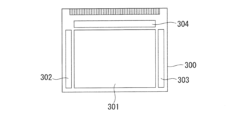
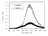
- 1 is a top view of a display device according to this embodiment; FIG. 1 is a schematic cross-sectional view of a TFT manufactured in an example; FIG. FIG. 10 is CL spectra measured in Example 217 and Comparative Example 20.
- film or “thin film” and the term “layer” can be interchanged depending on the case.
- oxide sintered body may be simply referred to as “sintered body”.
- sputtering target may be simply referred to as “target”.
- electrically connected includes the case of being connected via "something that has some electrical action”.
- something that has some kind of electrical action is not particularly limited as long as it enables transmission and reception of electrical signals between connection objects.
- things having some electrical action include electrodes, wirings, switching elements (such as transistors), resistive elements, inductors, capacitors, and other elements having various functions.
- source and drain functions of a transistor may be interchanged when using transistors with different polarities or when the direction of current changes in circuit operation. Therefore, the terms source and drain can be used interchangeably in this specification and the like.
- x to y represents a numerical range of "x or more and y or less”.
- the upper and lower limits recited for numerical ranges can be arbitrarily combined.
- the form which combined two or more of the individual forms of this invention described below is also the form of this invention.
- the crystalline oxide thin film according to this embodiment is a crystalline oxide thin film containing In as a main component.
- a low-resistance region A and a high-resistance region B having different spreading resistance values measured by a scanning spreading resistance microscope (SSRM) are provided, and the spreading resistance of the high-resistance region B is The value is eight times or more the spreading resistance value of the low resistance region A.
- the crystalline oxide thin film according to this embodiment is mainly composed of In element.
- Being the main component means that the composition ratio of In (atomic %: at %) is 50 at % or more with respect to all metal elements in the crystalline oxide thin film.
- the composition ratio of In is preferably 70 at % or more, more preferably 80 at % or more, and even more preferably 85 at % or more. If 50 at % or more of the total number of metal atoms constituting the crystalline oxide thin film is In element, sufficiently high mobility can be exhibited when the crystalline oxide thin film according to the present embodiment is employed for a TFT. .
- crystalline oxide thin films include H, B, C, N, O, F, Mg, Al, Si, O, S, Cl, Ar, Ca, Sc, Ti, V, Cr, Mn, Fe, Co, Ni, Cu, Zn, Ga, Ge, Y, Zr, Nb, Mo, Tc, Ru, Rh, Pd, Ag, Cd, Sn, Sb, Cs, Ba, Ln, Hf, Ta, W, Re, It may contain one or more elements selected from the group consisting of Os, Ir, Pt, Au, Pb and Bi.
- the crystalline oxide thin film may consist essentially of elements selected from In, Mg, Al, Si, Zn, Ga, Mo, Sn, Ln elements (lanthanoid elements) and O.
- the term “substantially” refers to the range in which the effects of the present invention due to the combination of In, Mg, Al, Si, Zn, Ga, Mo, Sn, Ln and O are produced, and This means that the crystalline oxide thin film may contain other components.
- the metal elements are In and Ga, and the atomic ratio satisfies the following formula (11). [Ga]/([In]+[Ga]) ⁇ 22at% (11)
- F or H may be included in addition to inevitable impurities and O.
- a more preferable second form of the crystalline oxide thin film includes In and B, Al, Sc, Mg, Zn, Ti, Y, Zr, Mo, Sn, Hf, W, Nb, and Ta as metal elements. , Ge, Si, La, Ce, Pr, Nd, Sm, Dy, Ho, Er, Tm, Yb and Lu.
- the ratio satisfies the following formula (12). [X]/([In]+[X]) ⁇ 15at% (12)
- F or H may be included in addition to inevitable impurities and O.
- the ratio of In increases, and the bixbite structure in which the In site is substituted with X can be crystallized even by annealing at a low temperature such as 300.degree. Furthermore, by adding the element X, which has a strong bonding force with oxygen, oxygen deficiency after annealing can be suppressed, and a film stable as a semiconductor can be formed.
- a more preferred third form of the crystalline oxide thin film includes metal elements In, Ga, B, Al, Sc, Mg, Zn, Ti, Y, Zr, Mo, Sn, Hf, W, Consists of one or more elements X selected from Nb, Ta, Ge, Si, La, Ce, Pr, Nd, Sm, Dy, Ho, Er, Tm, Yb and Lu, and metal elements other than In and Ga as additive elements
- X the atomic ratio satisfies the following formulas (13) and (14).
- a more preferred fourth form of the crystalline oxide thin film includes metal elements In, Sn, B, Al, Sc, Mg, Zn, Ti, Y, Zr, Mo, Hf, W, Nb, It consists of one or more elements X selected from Ta, Ge, Si, La, Ce, Pr, Nd, Sm, Dy, Ho, Er, Tm, Yb and Lu, and metal elements other than In and Sn are called element X , the atomic ratio satisfies the following formulas (15) and (16).
- F or H may be included in addition to inevitable impurities and O.
- the ratio of In is increased, and even with annealing at a low temperature such as 300° C., it is possible to crystallize into a bixbite structure in which the In sites are substituted with Sn. Since Sn has a large ion radius and orbital overlap with In is large, high mobility can be maintained. Further, by adding the additive element X having a strong bonding force with oxygen, the oxygen vacancies after annealing can be further suppressed, and a film stable as a semiconductor can be formed.
- a more preferable fifth form of the crystalline oxide thin film includes In, Zn, B, Al, Sc, Mg, Ti, Y, Zr, Mo, Hf, W, Nb, Ta, It consists of one or more elements X selected from Ge, Si, La, Ce, Pr, Nd, Sm, Dy, Ho, Er, Tm, Yb and Lu, and when the element X is a metal element other than In and Zn , the atomic ratio satisfies the following formulas (17) and (18).
- F or H may be included in addition to inevitable impurities and O.
- the ratio of In is increased, and the bixbite structure in which the In sites are substituted with Zn can be crystallized even by annealing at a low temperature such as 300.degree.
- Zn By adding Zn, the film immediately after the film formation can be made amorphous, and the film can be processed without residue during semiconductor patterning using acid during the fabrication of TFTs.
- an additive element X having a strong bonding force with oxygen oxygen vacancies after annealing can be suppressed, and a film stable as a semiconductor can be formed.
- the content (atomic ratio) of each metal element in the crystalline oxide thin film can be obtained by measuring the abundance of each element by ICP (Inductive Coupled Plasma) measurement or XRF (X-ray Fluorescence) measurement.
- ICP Inductive Coupled Plasma
- XRF X-ray Fluorescence
- ICP-OES inductively coupled plasma emission spectrometer
- a thin-film fluorescent X-ray analyzer AZX400, manufactured by Rigaku Corporation
- the content (atomic ratio) of each metal element in the crystalline oxide thin film was measured by TEM-EDS measurement using an electron microscope, ICP measurement using an inductively coupled plasma emission spectrometer, and sector-type dynamic secondary ion mass measurement. Analysis can be performed with an error accuracy within 2 atomic % by SIMS analysis using an analyzer.
- the metal elements in the crystal oxide thin film are identified by cross-sectional TEM-EDS, and the composition ratio is identified within an error range of about 10 atomic % by semi-quantitative analysis.
- a standard oxide thin film is prepared from 10 kinds of composition ratios with known atomic ratios of metal elements in the range of 20 atomic % from the results of semi-quantitative analysis.
- the value measured by the inductively coupled plasma emission spectrometer or the thin film fluorescence X-ray spectrometer is taken as the absolute value of the composition ratio.
- a source/drain electrode was formed with the same material as the TFT element and with the same channel length.
- the mass spectrum intensity of each element is obtained, and a calibration curve of known element concentrations and mass spectrum intensities is prepared.
- the oxide thin film portion of the actual TFT element taken out from the panel is subjected to SIMS analysis using a sector-type dynamic secondary ion mass spectrometer, and the atomic ratio is calculated from the spectral intensity using the calibration curve described above.
- the calculated atomic ratio can be confirmed with an accuracy within 2 atomic % of the atomic ratio of the oxide thin film separately measured by a thin film fluorescence X-ray spectrometer or an inductively coupled plasma emission spectrometer.
- the crystalline oxide thin film according to the present embodiment has a low resistance region A and a high resistance region B having different spreading resistance values measured by a scanning spreading resistance microscope (SSRM) in the plane direction of the crystalline oxide thin film,
- the ratio (R B /R A ) of the spreading resistance value RB of the high resistance region B to the spreading resistance value RA of the low resistance region A is 8 times or more.
- R B /R A is preferably 10 times or more, more preferably 15 times or more.
- a sufficient energy barrier is formed between the low-resistance region A and the high-resistance region B. Therefore, when a crystalline oxide thin film is used as the channel layer of a TFT, the DIBL phenomenon is suppressed.
- R B /R A is not particularly limited, it is, for example, 100,000 times or less, and may be 10,000 times or less. If RB / RA is too large, the energy barrier between the low-resistance region A and the high-resistance region B is too large, and thus becomes an electron injection barrier when a voltage Vd is applied between the source electrode and the drain electrode. , the mobility of the TFT is reduced.
- “high” and “low” of "resistance” mean the relative high and low of the spreading resistance value of the region A and the region B. As shown in FIG.
- the spreading resistance value RA of the low resistance region A is preferably 1 ⁇ or more and 1 ⁇ 10 6 ⁇ or less.
- the low-resistance region A is formed, for example, in the presence of indium-tin oxide (ITO), indium zinc oxide (IZO), aluminum, etc., by a method of heat treatment (annealing), plasma treatment, or ion implantation. can be formed by lowering the resistance of A region that is not subjected to the low-resistance treatment becomes a high-resistance region B.
- ITO indium-tin oxide
- IZO indium zinc oxide
- aluminum aluminum
- ion implantation ion implantation
- the thickness of the crystalline oxide thin film is preferably 80 nm or less.
- the thickness of the crystalline oxide thin film is preferably 60 nm or less, more preferably 50 nm or less, and particularly preferably 40 nm or less.
- the thickness of the crystalline oxide thin film is, for example, 3 nm or more, may be 5 nm or more, or may be 10 nm or more.
- the film thickness of the crystalline oxide thin film is measured based on a cross-sectional TEM observation image (sometimes referred to as a “cross-sectional TEM image”).
- the dC/dV value at the boundary between the low resistance region A and the high resistance region B is the dC/dV value of the high resistance region B Greater than value.
- the carrier concentration continuously changes at the boundary between the low-resistance region A and the high-resistance region B, and electrons are accumulated at the interface between the gate insulating film and the channel layer when the TFT is driven (here, Vg>0). There is no electrical potential barrier between the source and the drain in the state), and high mobility characteristics can be obtained. SCM measurement conditions will be described in detail in Examples.
- the average grain boundary angle ⁇ between the lower surface of the crystalline oxide thin film and the grain boundaries in the thin film is preferably 70° or more and 110° or less.
- the average grain boundary angle ⁇ between the thin film surface and the crystal grain boundaries in the thin film is measured based on a cross-sectional TEM observation image (sometimes referred to as a "cross-sectional TEM image"). That is, it is calculated by analyzing the angle formed between the crystal grain boundary and the thin film surface observed by cross-sectional TEM under magnification using a transmission electron microscope.
- the average distance D between crystal grain boundaries in the crystalline oxide thin film is preferably 0.01 ⁇ m or more and 2.0 ⁇ m or less.
- the small TFT having the crystalline oxide thin film according to the present embodiment exhibits high mobility, and uniform characteristics of mobility and threshold voltage (Vth) with respect to device shape can be obtained.
- Vth threshold voltage
- the average distance D between crystal grain boundaries in the thin film is measured based on the cross-sectional TEM observation image. Measurement conditions will be described in detail in Examples.
- the crystalline oxide thin film contains crystal grains having a bixbite structure in electron beam diffraction. Since the crystal grains of the bixbite structure are cubic crystals with good symmetry, it is possible to suppress deterioration of TFT characteristics (mobility) even across crystal grain boundaries.
- the crystal oxide thin film of the present embodiment is a crystal oxide thin film containing In as a main component, and has a thickness of 80 nm or less.
- a high carrier concentration region A and a low carrier concentration region B having different carrier concentrations are provided in the plane direction of the crystalline oxide thin film, and the carrier concentration of the high carrier concentration region A is 10 19 cm ⁇ 3 or more and 10 22 cm ⁇ 3 . 3 or less, and the carrier concentration of the high carrier concentration region A is 8 times or more the carrier concentration of the low carrier concentration region B. It is preferably 10 times or more, more preferably 15 times or more, and still more preferably 100 times or more.
- an energy barrier is formed between the low-resistance region and the high-resistance region.
- the crystalline oxide thin film is defined by a high carrier concentration region A and a low carrier concentration region B instead of the low resistance region A and the high resistance region B of the crystalline oxide thin film of the first embodiment.
- the high carrier concentration region A corresponds to the low resistance region A
- the low carrier concentration region B corresponds to the high resistance region B.
- the film thickness of the crystalline oxide thin film is 80 nm or less.
- the thickness of the crystalline oxide thin film is preferably 60 nm or less, more preferably 50 nm or less, and particularly preferably 40 nm or less.
- the thickness of the crystalline oxide thin film is, for example, 3 nm or more, may be 5 nm or more, or may be 10 nm or more.
- the carrier concentration of the high carrier concentration region A is 10 19 cm ⁇ 3 or more and 10 22 cm ⁇ 3 or less, preferably 10 19 cm ⁇ 3 or more and 10 21 cm ⁇ 3 or less.
- the carrier concentration of the low carrier concentration region B is preferably 10 15 cm ⁇ 3 or more and less than 10 19 cm ⁇ 3 .
- the constituent elements, manufacturing method, preferred range, etc. of the crystalline oxide thin film according to this embodiment are the same as those of the first embodiment.
- the crystalline oxide thin film of the first embodiment has been described, but the same applies to the second embodiment. Applicable. Specifically, by replacing the low resistance region A with the high carrier concentration region A and the high resistance region B with the low carrier concentration region B, the application example of the second embodiment is obtained.
- the crystalline oxide thin film of the present embodiment is a crystalline oxide thin film containing In as a main component, has a thickness of 80 nm or less, and has crystals of the crystalline oxide thin film.
- the average distance D between grain boundaries is 2 ⁇ m or less, and the carrier concentration is 10 19 cm ⁇ 3 or more and 10 22 cm ⁇ 3 or less.
- the crystalline oxide thin film of this embodiment has the high carrier concentration region A of the crystalline oxide thin film of the second embodiment.
- the constituent elements, manufacturing method, preferred range, etc. of the crystalline oxide thin film according to this embodiment are the same as those of the first and second embodiments.
- Laminate A laminate according to the present embodiment has the crystalline oxide thin film according to the embodiment described above and a lower layer that supports the crystalline oxide thin film.
- FIG. 1 is a schematic cross-sectional view of a laminate as an example of the present embodiment.
- the laminate 10 has a crystalline oxide thin film 11 and a lower layer 12 supporting the crystalline oxide thin film 11 .
- the crystal oxide thin film 11 has one high resistance region B (11B) and two low resistance regions A (11A) sandwiching the high resistance region B (11B) in the plane direction.
- FIG. 2 is a schematic cross-sectional view of a laminate of another example of the present embodiment.
- the stack 20 has a crystalline oxide thin film 11 and a lower layer 12 supporting the crystalline oxide thin film 11 .
- the crystalline oxide thin film 11 has high-resistance regions B (11B) and low-resistance regions A (11A) alternately formed in the plane direction.
- the lower layer 12 is a single layer, but is not limited to this, and may be a laminate of two or more layers.
- the lower layer 12 includes a substrate, a buffer layer, an insulating layer, an electrode, a light shield layer, and the like. Each of these may be composed of two or more layers.
- the average grain boundary angle ⁇ sub between the surface of the lower layer and the crystal grain boundaries in the crystalline oxide thin film is preferably 70° or more and 110° or less.
- the average grain boundary angle ⁇ sub between the surface of the lower layer and the crystal grain boundaries in the crystalline oxide thin film satisfies the above range, the crystal grain boundaries are formed with respect to the surface of the lower layer with which the crystalline oxide thin film is in contact. can exist in secret.
- an electrode for example, a source electrode
- crystal grain boundaries are densely present with respect to the electrode surface.
- the contact area with the electrode is narrow (for example, a small TFT)
- electron injection into the crystalline oxide thin film can be ensured, and a decrease in mobility can be suppressed.
- the crystalline oxide thin film of the present embodiment and the laminated body including the crystalline oxide thin film include, for example, a substrate, a buffer layer, an insulating layer, and the like, in which the lower layers constituting the TFT are composed mainly of In oxide. It can be manufactured by forming a thin film and then subjecting desired portions to the above-described resistance reduction treatment.
- the film formation method is not particularly limited, for example, DC sputtering, AC sputtering, RF sputtering, ICP sputtering, reactive sputtering, ion plating, ALD, PLD, MO-CVD, ICP-CVD, sol-gel method, coating method, mist CVD can be mentioned.
- the film may be formed using a planar sputtering cathode device or a rotary sputtering cathode device.
- a film is formed by DC sputtering using a sputtering target containing an oxide sintered body containing an oxide of In as a main component, and then a desired portion is subjected to the above-described low resistance treatment.
- the atomic composition ratio of the crystalline oxide thin film obtained by the sputtering method reflects the atomic composition ratio of the oxide sintered body in the sputtering target. Therefore, it is preferable to form a film using a sputtering target containing an oxide sintered body having an atomic composition ratio similar to that of the desired oxide thin film.
- heat treatment may be performed before the resistance reduction treatment.
- the heat treatment process is not particularly limited, but a hot air furnace, an IR furnace, a lamp annealing device, a laser annealing device, a thermal plasma device, or the like can be used.
- plasma oxidation treatment with N 2 O or plasma oxidation treatment with O 2 may be performed before the low resistance treatment.
- the apparatus for plasma oxidation treatment is not particularly limited, but PE-CVD and the like can be mentioned.
- the target used in the sputtering method preferably has an impurity metal content of 500 ppm or less, more preferably 100 ppm or less.
- the content of impurity metals in the target can be measured by ICP or SIMS as in the case of the crystalline oxide thin film.
- Impurities contained in the target are elements that are not intentionally added and are mixed in raw materials or in the manufacturing process, and are trace elements that do not substantially affect the performance of the target and semiconductor. ” means an element that is a metal element among the elements as “impurities”.
- the sputtering target may consist essentially of In and an element selected from Mg, Al, Si, Zn, Ga, Mo, Sn, Ln elements (lanthanoid elements) and O.
- the term “substantially” means that the sputtering target is within the range where the effects of the present invention due to the combination of Mg, Al, Si, Zn, Ga, Mo, Sn, Ln and O other than In are produced. , means that it may contain other ingredients.
- a more preferable first form of the sputtering target is an oxide in which the metal elements are In and Ga, and the atomic ratio is the following formula (11) meet. [Ga]/([In]+[Ga]) ⁇ 22at% (11)
- a more preferred second form of the sputtering target includes In and B, Al, Sc, Mg, Zn, Ti, Y, Zr, Mo, Sn, Hf, W, Nb, Ta, Ge, Si, La, An oxide composed of one or more elements X selected from Ce, Pr, Nd, Sm, Dy, Ho, Er, Tm, Yb, and Lu, where X is a metal element other than In, as an atomic ratio It satisfies the following formula (12). [X]/([In]+[X]) ⁇ 15at% (12)
- a more preferred third form of the sputtering target contains In, Ga, B, Al, Sc, Mg, Zn, Ti, Y, Zr, Mo, Sn, Hf, W, Nb, Ta, Ge, and Si as metal elements. , La, Ce, Pr, Nd, Sm, Dy, Ho, Er, Tm, Yb and Lu. , the atomic ratio satisfies the following formulas (13) and (14). [Ga]/([In]+[Ga]+[X]) ⁇ 22.5 at % (13) [X]/([In]+[Ga]+[X]) ⁇ 8.0at% (14)
- a more preferred fourth form of the sputtering target contains In, Sn, B, Al, Sc, Mg, Zn, Ti, Y, Zr, Mo, Hf, W, Nb, Ta, Ge, Si, and La as metal elements. , Ce, Pr, Nd, Sm, Dy, Ho, Er, Tm, Yb, and Lu, where the element X is a metal element other than In and Sn
- the atomic ratio satisfies the following formulas (15) and (16). [Sn]/([In]+[Sn]+[X]) ⁇ 20at% (15) [X]/([In]+[Sn]+[X]) ⁇ 8.0at% (16)
- a more preferred fifth form of the sputtering target contains In, Zn, B, Al, Sc, Mg, Ti, Y, Zr, Mo, Hf, W, Nb, Ta, Ge, Si, La, and Ce as metal elements. , Pr, Nd, Sm, Dy, Ho, Er, Tm, Yb and Lu.
- the atomic ratio satisfies the following formulas (17) and (18). [Zn]/([In]+[Zn]+[X]) ⁇ 12at% (17) [X]/([In]+[Zn]+[X]) ⁇ 8.0at% (18)
- An oxide thin film obtained by sputtering using a sputtering target containing indium oxide as a main component is an amorphous oxide thin film.
- This oxide thin film is patterned into islands by photolithography, and heated to crystallize before forming a protective film, thereby obtaining a crystalline oxide thin film in which surface crystals have a single crystal orientation. can. Each step will be described below.
- the above-described sputtering target is used, and one or more gases selected from the group consisting of argon and oxygen substantially free of impurity gases are used as the sputtering gas to form the oxide thin film by sputtering. to form a film.
- the sputtering target is preferably mounted in an RF magnetron sputtering device or a DC magnetron sputtering device for sputtering.
- the sputtering gas substantially does not contain impurity gases
- the gases other than the sputtering gas are excluded, excluding adsorbed water brought in when the gas is inserted, and gases that cannot be eliminated (inevitable impurity gases) such as chamber leaks and adsorbed gases.
- the impurity gas is not actively introduced. Impurities are preferably excluded from the gas (sputtering gas) introduced during sputtering film formation, if possible.
- the impurity gas content in the sputtering gas is preferably 0.1% by volume or less, more preferably 0.05% by volume or less. If the proportion of the impurity gas is 0.1% by volume or less, crystallization of the oxide thin film proceeds without problems.
- the purity of high-purity argon and high-purity oxygen, which are examples of the sputtering gas, is preferably 99% by volume or higher, more preferably 99.9% by volume or higher, and even more preferably 99.99% by volume or higher.
- the gas (sputtering gas) to be introduced during sputtering film formation is not particularly limited, but examples thereof include argon, nitrogen, oxygen, water, hydrogen, and a mixed gas containing two or more of these gases.
- the oxygen partial pressure in the mixed gas is preferably more than 0% by volume and 50% by volume or less, more preferably more than 0% by volume and 20% by volume or less. . If the oxygen partial pressure is more than 0% by volume and 50% by volume or less, the material is easily crystallized into a semiconductor when heated. By changing the oxygen partial pressure, the degree of oxidation of the oxide thin film, that is, the degree of crystallization can be adjusted.
- the oxygen partial pressure may be appropriately selected as required.
- the water pressure in the mixed gas is preferably more than 0.03% by volume and 10% by volume or less, and more than 0.03% by volume and 5% by volume or less. more preferred.
- the water pressure is more than 0.03% by volume and 5% by volume or less, the material is easily crystallized to become a semiconductor when heated.
- a mixed gas of hydrogen and oxygen may be used instead of water.
- the crystalline oxide thin film according to the present embodiment preferably contains In element as a main component.
- This oxide thin film By heating this oxide thin film in a heat treatment step to be described later, columnar crystals can be grown on the lower layer.
- the oxide thin film formed as described above By applying the oxide thin film formed as described above to a small TFT, the electron carrier injection property is excellent during driving, resulting in high mobility, and the device shape of mobility and threshold voltage (Vth). uniform characteristics for
- Step of Forming TFT Constituent Layers When forming TFT constituent layers such as an insulating layer on the crystalline oxide thin film, it is preferable to form the constituent layers on the oxide thin film after heat-treating the obtained oxide thin film. . By performing annealing before forming the constituent layers of the TFT, oxygen and hydrogen are diffused at the time of annealing, and high-quality columnar crystals are obtained. A TFT is obtained.
- Heat treatment process After forming the oxide thin film, a heat treatment is performed. This heat treatment is sometimes called annealing.
- the heat treatment temperature is preferably 250° C. or higher and 500° C. or lower, more preferably 280° C. or higher and 470° C. or lower, and even more preferably 300° C. or higher and 450° C. or lower. If the heat treatment temperature after forming the oxide thin film is 250° C. or higher, the oxide thin film is easily crystallized. If the heat treatment temperature after forming the oxide thin film is 500° C. or less, it is possible to prevent abnormal growth of crystals and increase the size of the crystal grains, and control the crystal grain size to be small.
- the heating time in the heat treatment step is preferably 0.1 hours or more and 5 hours or less, more preferably 0.3 hours or more and 3 hours or less, and 0.5 hours or more and 2 hours or less. is more preferred. If the heating time in the heat treatment step is 0.1 hour or longer, the oxide thin film is easily crystallized without crystallization. If the heating time in the heat treatment step is 5 hours or less, it is economical.
- the term "heating time” refers to the time (holding time) during which a predetermined maximum temperature is maintained during heat treatment.
- the heating rate in the heat treatment step is preferably 2° C./min or more and 40° C./min or less, and more preferably 3° C./min or more and 20° C./min or less. If the heating rate in the heat treatment step is 2° C./min or more, the production efficiency of the oxide thin film is improved as compared with the case of less than 1° C./min. If the heating rate in the heat treatment step is 40° C./min or less, the metal elements are uniformly diffused during crystallization, and crystals in which the metal is not segregated at grain boundaries can be formed. Also, the heating rate in the heat treatment process is a value obtained by dividing the actual temperature of the oxide thin film by time, unlike the value calculated from the set temperature and set time of the furnace. The actual temperature of the oxide thin film can be determined, for example, by measuring an area within 1 cm of the oxide thin film in the furnace with a thermocouple.
- the heat treatment process is performed in an air atmosphere with a humidity of 10% or more at 25°C.
- the heat treatment step is performed in the atmosphere with a humidity of 10% or more, hydrogen and oxygen diffuse into the film during annealing, and crystallization can be promoted.
- the heat treatment process is preferably performed after patterning the oxide thin film.
- crystallization can be promoted while excess oxygen present in the film during film formation and organic matter adhering during patterning are eliminated.
- Crystal defects in the film after heat treatment can be evaluated by defect analysis such as cathodoluminescence (CL).
- CL cathodoluminescence
- the heat treatment process may be performed multiple times. For example, after patterning the oxide thin film, the heat treatment step (first heat treatment step) described above may be performed, and after manufacturing the TFT element, the heat treatment step (second heat treatment step) may be performed as the final step.
- the second heat treatment step is preferably performed at a higher annealing temperature than the first heat treatment step.
- a low resistance region A and a high resistance region B are formed in the crystalline oxide thin film obtained in the heat treatment step.
- the low-resistance region A is not particularly limited, but for example, in the presence of indium tin oxide (ITO), aluminum, etc., a method of heat treatment (annealing), a plasma treatment, a dry process such as ion implantation, etc. It can be formed by lowering the resistance of the part.
- a region that is not subjected to the low-resistance treatment becomes a high-resistance region B.
- an ITO layer is formed by sputtering or the like on the crystal oxide thin film in the region where the resistance is to be reduced, and then heated to 250° C. or higher and 500° C. or lower (annealing may be performed at a temperature of preferably 280° C. or more and 470° C. or less, more preferably 300° C. or more and 450° C. or less for a time of 0.1 hour or more and 5 hours or less. After annealing, the ITO layer may be etched away or left in place.
- an aluminum layer is formed by sputtering or the like on the crystal oxide thin film in the region where the resistance is to be reduced, and then heated to 250° C. or more and 500° C. or less (annealing may be performed at a temperature of preferably 280° C. or more and 470° C. or less, more preferably 300° C. or more and 450° C. or less for a time of 0.1 hour or more and 5 hours or less. After annealing, it may remain as aluminum or become aluminum oxide. In either case, the aluminum or aluminum oxide layer may be removed by etching or may be left as it is.
- the crystalline oxide thin film obtained in the heat treatment step is treated.
- Gases used for plasma processing are not particularly limited, but examples include H 2 , He, Ar, N 2 , F-based gases, and the like.
- Elements used for plasma treatment are generally preferably elements with small ionic radii. By performing plasma treatment using these elements, oxygen vacancies are generated in the crystalline oxide thin film, the carrier concentration is increased, and the resistance is lowered.
- ions may be implanted through the Ions used for implantation are not particularly limited, but examples include H + , He + , B + , N + , F + , PHx + , and Ar + . Any element that generates oxygen vacancies by ion implantation or an element that emits electrons and acts as a donor when left in the film may be used. Also, the element may or may not remain in the film.
- the low-resistance treatment step is preferably performed after forming the gate insulating film and/or the gate electrode.
- the low resistance region A and the high resistance region B can be formed using a gate insulating film and/or a gate electrode instead of a mask (self-alignment).
- the region where the ITO layer is directly laminated in the crystalline oxide thin film becomes the low resistance region A, and the region under the gate insulating film and/or the gate electrode becomes the high resistance region B. Become.
- a TFT according to this embodiment includes the crystalline oxide thin film or laminate of the present invention described above.
- the crystalline oxide thin film of the present invention is used as a channel layer of a TFT. More preferably, both ends of the channel layer, that is, the vicinity of the regions where the source and drain electrodes are connected are the low-resistance regions A of the crystalline oxide thin film, and the region in contact with the lower surface of the gate insulating film is the high-resistance region. B is preferred.
- a TFT has a channel layer, a source electrode and a drain electrode respectively connected to both ends of the channel layer, and a gate electrode stacked on the channel layer via a gate insulating film
- the channel layer is a crystalline oxide thin film, and has a structure in which a gate insulating film is formed in a high resistance region B and a source electrode and a drain electrode are formed in a low resistance region A.
- the distance L off from the end of the source electrode and the end of the drain electrode to the intersection of the perpendicular line drawn in the thickness direction from the end of the gate electrode and the crystalline oxide thin film is 4 ⁇ m or more and 20 ⁇ m or less.
- the average distance D between crystal grain boundaries of the crystalline oxide thin film and the distance Loff satisfy the following formula (1). 2 ⁇ L off /D ⁇ 100 (1)
- the TFT has a contact region length Ls between the source and drain electrodes and the channel layer of 4 ⁇ m or more and 20 ⁇ m or less.
- the average distance D between crystal grain boundaries of the crystalline oxide thin film and the contact region length Ls satisfy the following formula (2). 1 ⁇ Ls/D ⁇ 100 (2) As a result, excellent mobility is exhibited even if the contact regions between the source and drain electrodes and the channel layer are small.
- TFTs manufactured in the prior art use a crystalline oxide thin film in order to obtain high mobility.
- the length of the contact region between the source electrode and the oxide thin film was about 100 ⁇ m. Therefore, even if the crystal grain size of the oxide thin film is 1 ⁇ m or more, about 100 crystal grain boundaries are present in the contact region with the source electrode, and the crystal grain boundaries that are conductive regions with respect to the source electrode are present. A sufficient number were in contact with each other, and there was no major problem from the viewpoint of mobility.
- the conventional technology has a structure in which parasitic capacitance is generated in the region where the gate electrode and the source and drain electrodes overlap. Therefore, it was not a big problem.
- displays such as OLEDs are required to have high resolution, high-speed driving, and large area.
- the size of TFTs is becoming smaller. Therefore, it is necessary to control the characteristics of small TFTs patterned by photolithography, instead of film formation using a metal mask as in the conventional art.
- parasitic capacitance is reduced in order to eliminate the RC delay that delays the time from input to driving due to the effects of parasitic resistance and parasitic capacitance in the backplane drive circuit.
- it is necessary to reduce variations in parasitic capacitance as much as possible in order to eliminate luminance unevenness in each pixel of the OLED.
- the gate electrode is used as a mask to selectively lower the resistance of the semiconductor, and the regions are used as the source and drain regions.
- the oxide thin film is applied to a self-aligned small TFT structure (self-aligned small TFT structure)
- the length of the contact region between the source electrode and the crystalline oxide thin film is shortened.
- the intersection of the perpendicular drawn from the edge of the gate electrode in the thickness direction and the crystalline oxide thin film becomes shorter from the edge of the source electrode and the edge of the drain electrode.
- the edges of the source electrode and the drain electrode A sufficient number of crystal grain boundaries exist in the region from the edge to the intersection of the perpendicular line drawn in the thickness direction from the edge of the gate electrode and the crystal oxide thin film, and in the contact region with the source electrode. A sufficient number of grain boundaries must be present. According to the TFT according to the present embodiment, since the distance L off , the contact region length Ls, the formulas (1) and (2) are satisfied, the mobility is excellent and the Vth can be stably controlled.
- the horizontal gap ⁇ L between the low resistance region A and the gate electrode is less than 1 ⁇ m. Since the crystalline oxide thin film of the present invention is suitable for self-aligned TFTs, the gap ⁇ L can be made extremely small.
- the TFT according to this embodiment can be manufactured by adopting the above-described method for manufacturing the crystalline oxide thin film and laminate. That is, a sputtering target is used, and one or more gases selected from the group consisting of argon, nitrogen, hydrogen, water, and oxygen substantially free of impurity gases are used as the sputtering gas to form an oxide thin film by sputtering.
- This manufacturing method includes a step of forming a film (sometimes referred to as a film forming step) and a step of heat-treating the oxide thin film (sometimes referred to as a heat-treating step). Each condition of the film forming process and the heat treatment process is as described above.
- the source electrode, drain electrode, gate electrode and gate insulating film can be formed using known materials and forming methods.
- a crystalline oxide thin film according to one embodiment has a high mobility in a direction parallel to the film surface.
- a crystalline oxide thin film for the oxide semiconductor layer (channel layer) or conductive region of a small self-aligned TFT, high mobility and stable control of Vth can be achieved.
- a transfer characteristic Id-Vg graph is created when each Vd is applied, the transconductance (Gm) of each Vg is calculated, and the mobility is obtained using the linear region or saturation region equation.
- Current Id is the current between the source and drain electrodes
- voltage Vd is the voltage applied between the source and drain electrodes (drain voltage)
- voltage Vg is the voltage applied between the source and gate electrodes. (gate voltage).
- the mobility is 20 cm 2 /(V ⁇ s) or more, and the higher the mobility, the better.
- an ohmic electrode such as metal, ITO, or IZO is arranged on one surface of the high resistance region B, and the other surface has a work function of 4.8 eV or more.
- Schottky barrier diodes, MES-FETs, etc. can be configured by arranging Schottky electrodes of oxide or the like.
- the shape of the thin film transistor according to the present embodiment is not particularly limited as long as it is self-aligned, but a top gate type transistor, a back channel etch type transistor, an etch stopper type transistor, or the like is preferable.
- FIG. 3A is a schematic cross-sectional view of an example of the TFT of this embodiment.
- the TFT 50 is a top-gate type TFT, and includes a substrate 21, a buffer layer 22, a channel layer (a crystalline oxide thin film) 11, an ITO layer 23, a gate insulating film 24, a gate electrode 25, an interlayer insulating film 26, a source electrode 27, It has a drain electrode 28 and a protective film 29 .
- the TFT 50 has a structure in which a substrate 21, a buffer layer 22, and a channel layer (crystalline oxide thin film) 11 are laminated in this order.
- a high resistance region 11B is provided in the central portion of the channel layer 11, and a gate insulating film 24 and a gate electrode 25 are laminated in this order on the high resistance region 11B.
- the gate insulating film 24 is an insulating film that interrupts conduction between the gate electrode 25 and the crystalline oxide thin film 11 .
- Low resistance regions 11A-1 and 11A-2 of the channel layer 11 are present on both sides of the high resistance region 11B.
- the low resistance regions 11A-1 and 11A-2 and the gate electrode 25 are covered with an ITO layer 23 and an interlayer insulating film 26. As shown in FIG.
- the ITO layer 23 is used when forming the low resistance region of the channel layer 11 .
- a source electrode 27 and a drain electrode 28 are connected to the low resistance regions 11A-1 and 11A-2, respectively, through contact holes provided in the ITO layer 23 and the interlayer insulating film 26 .
- the source electrode 27 and the drain electrode 28 are conductive terminals for allowing source current and drain current to flow through the channel layer 11 .
- a protective film 29 is provided so as to cover the TFT constituent layers such as the interlayer insulating film 26, the source electrode 27, the drain electrode 28, and the like.
- FIG. 3B is an enlarged view of the vicinity of the source electrode in FIG. 3A.
- FIG. 3B shows the distance L off from the edge of the source electrode and the edge of the drain electrode to the intersection of the perpendicular line drawn in the thickness direction from the edge of the gate electrode and the crystalline oxide thin film in the TFT 50 , the source electrode
- the contact region length Ls between (the drain electrode) and the channel layer and the horizontal gap ⁇ L between the low resistance region A and the gate electrode are illustrated.
- FIG. 4 is a schematic cross-sectional view of another example of the TFT of this embodiment.
- the TFT 51 has the same configuration as the TFT 50 except that the write shield layer 31 is provided between the substrate 21 and the buffer layer 22 .
- the light shield layer 31 is formed to suppress malfunction of the TFT due to light.
- FIG. 5 is a schematic cross-sectional view of another example of the TFT of this embodiment.
- the TFT 52 has the same configuration as the TFT 50 except that the ITO layer 23 is not formed.
- the low resistance regions 11A-1 and 11A-2 are formed by, for example, an ion implantation method or a dry process such as plasma processing.
- FIG. 6 is a schematic cross-sectional view of another example of the TFT of this embodiment.
- the TFT 60 has the same configuration as the TFT 50 except that the ITO layer 23 is not formed and the interlayer insulating film 26 has a two-layer structure (interlayer insulating films 26-1 and 26-2).
- the region under the gate electrode 25 of the interlayer insulating film 26-1 corresponds to the gate insulating film 24.
- the low resistance regions 11A-1 and 11A-2 are formed by ion implantation, for example.
- FIG. 7 is a schematic cross-sectional view of another example of the TFT of this embodiment.
- the TFT 70 is a bottom-gate type TFT, and includes a substrate 21, a gate electrode 25, a gate insulating film 24, a channel layer (a crystalline oxide thin film) 11, an interlayer insulating film 26, a source electrode 27, a drain electrode 28, and a protective film 29. have.
- the gate electrode 25 is formed on the substrate 21 and the gate insulating film 24 is laminated on the substrate 21 and the gate electrode 25 .
- a channel layer (crystalline oxide thin film) 11 is laminated on the gate insulating film 24, a region corresponding to the gate electrode 25 is a high resistance region 11B, and low resistance regions of the channel layer 11 are formed on both sides of the high resistance region 11B.
- the channel layer (crystalline oxide thin film) 11 is covered with an interlayer insulating film 26 .
- a source electrode 27 and a drain electrode 28 are connected to the low-resistance regions 11A-1 and 11A-2, respectively, through contact holes provided in the interlayer insulating film 26 .
- a protective film 29 is provided so as to cover the TFT constituent layers such as the interlayer insulating film 26 , the source electrode 27 and the drain electrode 28 .
- the TFT of this embodiment can be improved with a known configuration.
- any commonly used material can be selected.
- a glass substrate, a ceramic substrate, a quartz substrate, or a sapphire substrate can be used. It is also possible to apply a single crystal semiconductor substrate such as silicon or silicon carbide, a polycrystalline semiconductor substrate, a compound semiconductor substrate such as silicon germanium, an SIO (Silicon In Insulator) substrate, or the like. You may use the thing provided with the element as a board
- a flexible substrate may also be used as the substrate.
- the method of providing a TFT on a flexible substrate in addition to the method of directly fabricating a TFT on a flexible substrate, after fabricating a TFT on a non-flexible substrate, the TFT is peeled off to form a flexible substrate. There is also a method of setting it on the board. In that case, a release layer may be provided between the non-flexible substrate and the TFT.
- the material for forming the buffer layer 22 is not particularly limited, and generally used materials can be arbitrarily selected, and a laminated film can be used.
- the buffer layer 22 can be appropriately designed according to the type of substrate.
- the write shield layer 31 may be connected to the source electrode 27 or may be connected to the gate electrode 25 .
- the material for forming the write shield layer is not particularly limited, and any commonly used material can be selected. Specifically, metal electrodes such as Al, Ag, Cu, Cr, Ni, Co, Mo, Au, Ti, Zr, Ru, Y, Nb, Ta, W, and metals made of alloys containing two or more of these metals An electrode etc. are mentioned. A laminated electrode having two or more layers can also be used.
- a second buffer layer may be provided between the write shield layer 31 and the substrate 21 .
- the material for forming the second buffer layer is not particularly limited, and generally used materials can be arbitrarily selected, and a laminated film can be used.
- Materials for forming the gate insulating film are not particularly limited, and generally used materials can be arbitrarily selected, and a laminated film can be used.
- the crystalline oxide thin film as the channel layer for the source electrode and the drain electrode has a channel length (L length) of 1 ⁇ m or more and 50 ⁇ m or less.
- the channel width is not particularly limited, for example, the channel width (W length) is 1 ⁇ m or more and 1000 ⁇ m or less.
- Materials for forming the drain electrode, the source electrode and the gate electrode are not particularly limited, and commonly used materials can be arbitrarily selected. Specifically, transparent electrodes such as ITO, IZO, ZnO, SnO2 , metals such as Al, Ag, Cu, Cr, Ni, Co, Mo, Au, Ti, Zr, Ru, Y, Nb, Ta, W Electrodes, metal electrodes made of alloys containing two or more of these metals, and the like. A laminated electrode having two or more layers can also be used.
- each interlayer insulating film Materials for forming each interlayer insulating film are not particularly limited, and generally used materials can be arbitrarily selected, and laminated films can be used.
- the drain electrode, the source electrode and the conductive region regardless of the structure of the TFT. Furthermore, in the case of the bottom gate type, it is preferable to provide a protective film on the channel layer. By providing the protective film, the durability can be easily improved even when the TFT is driven for a long time.
- TEOS Tetraethoxysilane
- SiH 4 silane
- the protective film or the insulating film when forming by PE-CVD, it may be a high-temperature process.
- the protective film or the insulating film often contains impurity gas immediately after being formed, it is preferable to perform heat treatment (annealing treatment).
- annealing treatment By removing the impurity gas by heat treatment, a stable protective film or insulating film can be obtained, making it easier to form a highly durable TFT.
- annealing after forming the gate insulating film hydrogen contained in the gate insulating film diffuses to the oxide thin film, and crystal defects present on the surface of the oxide thin film are terminated with hydroxyl groups, resulting in fewer electron traps. Oxide thin films with good conductive properties can be formed.
- the crystalline oxide thin film of the present invention By using the crystalline oxide thin film of the present invention, the effect of the temperature in the PE-CVD process and the effect of the subsequent heat treatment are reduced, so even if a protective film or an insulating film is formed, the TFT characteristics stability can be improved.
- the threshold voltage (Vth) is preferably -3.0 V or more and 3.0 V or less, more preferably -2.0 V or more and 2.0 V or less, and even more preferably -1.0 V or more and 1.0 V or less. If the threshold voltage (Vth) is ⁇ 3.0 V or more and 3.0 V or less, it is possible to correct Vth to 0 V by mounting a Vth correction circuit on the TFT. When the TFT thus obtained is mounted on a panel, it is possible to drive the display without unevenness in brightness and burn-in.
- the on-off ratio is preferably 10 6 or more and 10 12 or less, more preferably 10 7 or more and 10 11 or less, and even more preferably 10 8 or more and 10 10 or less.
- a liquid crystal display can be driven when the on-off ratio is 10 6 or more.
- the on-off ratio is 10 12 or less, it is possible to drive an organic EL device with high contrast.
- the off current can be 10 ⁇ 12 A or less, and when used for the transfer transistor or reset transistor of a CMOS image sensor, the image retention time can be lengthened and the sensitivity can be improved. You can improve it.
- the OFF current value is preferably 10 ⁇ 10 A or less, more preferably 10 ⁇ 11 A or less, and even more preferably 10 ⁇ 12 A or less.
- an organic EL with high contrast can be driven.
- it is used as a transfer transistor or a reset transistor of a CMOS image sensor it is possible to lengthen the image holding time and improve the sensitivity.
- the TFT according to the present embodiment can be suitably used in electronic devices such as display elements such as solar cells, liquid crystal elements, organic electroluminescence elements and inorganic electroluminescence elements, power semiconductor elements, and touch panels.
- display elements such as solar cells, liquid crystal elements, organic electroluminescence elements and inorganic electroluminescence elements, power semiconductor elements, and touch panels.
- the thin film transistor according to the present embodiment can also be applied to various integrated circuits such as field effect transistors, logic circuits, memory circuits, and differential amplifier circuits, and can be applied to electronic devices and the like. Furthermore, the thin film transistor according to the present embodiment can be applied not only to field effect transistors but also to electrostatic induction transistors and Schottky barrier transistors.
- the thin film transistor according to this embodiment can be suitably used for a display device such as a portable display device or an in-vehicle display device, a solid-state imaging device, and the like.
- the thin film transistor according to the present embodiment can also be suitably used as a transistor for a flat panel detector for an X-ray image sensor for medical use.
- the crystalline oxide thin film according to this embodiment can also be applied to Schottky diodes, resistance change memories, and resistance elements. A case where the thin film transistor according to this embodiment is used in a display device will be described below.
- FIG. 8A is an example of a circuit diagram of a pixel portion when a liquid crystal element is applied. When this is used for a Mini LED display, FIG. 8A can be used not only for the liquid crystal control circuit but also for the LED chip control circuit.
- FIG. 8B is an example of a circuit diagram of a pixel portion when an organic EL element is applied.
- the circuit of the pixel section can be applied to a configuration in which one pixel has a plurality of pixel electrodes. Each pixel electrode is connected to a different transistor, and each transistor is configured to be driven by a different gate signal. As a result, the signals applied to the individual pixel electrodes of the pixels designed for multi-domains can be independently controlled.
- At least one of the transistors in the circuit diagram may be the TFT according to this embodiment.
- the circuit diagram is not limited to the configurations shown in FIGS. 8A and 8B.
- switches, resistive elements, capacitive elements, transistors, sensors, or logic circuits may be added.
- both the Si-based transistor and the TFT according to this embodiment may be mounted.
- FIG. 8C is a top view of the display device according to this embodiment.
- the thin film transistor according to this embodiment can be used as the transistor arranged in the pixel portion. Since the thin film transistor according to this embodiment can easily be of n-channel type, a part of a driver circuit that can be configured with n-channel type transistors is formed on the same substrate as the transistors in the pixel portion. By using the thin film transistor described in this embodiment mode for the pixel portion and the driver circuit, a highly reliable display device can be provided.
- FIG. 8C An example of a top view of an active matrix display device is shown in FIG. 8C.
- a pixel portion 301, a first scanning line driver circuit 302, a second scanning line driver circuit 303, and a signal line driver circuit 304 are formed over a substrate 300 of the display device.
- a plurality of signal lines are arranged extending from a signal line driver circuit 304
- a plurality of scanning lines are extended from a first scanning line driver circuit 302 and a second scanning line driver circuit 303 .
- Pixels each having a display element are provided in a matrix at intersection regions of the scanning lines and the signal lines.
- the substrate 300 of the display device is connected to a timing control circuit (also called a controller or control IC) via a connecting portion such as an FPC (Flexible Printed Circuit).
- a timing control circuit also called a controller or control IC
- FPC Flexible Printed Circuit
- the first scanning line driving circuit 302, the second scanning line driving circuit 303, and the signal line driving circuit 304 are formed on the same substrate 300 as the pixel portion 301.
- the number of parts such as a driving circuit provided outside is reduced, so that the cost can be reduced.
- the drive circuit is provided outside the substrate 300, it becomes necessary to extend the wiring, and the number of connections between the wirings increases.
- the number of connections between wirings can be reduced, and reliability or yield can be improved.
- Example 1 A thin film transistor (TFT) 53 shown in FIG. 9 was manufactured by the following steps. Note that the TFT 53 has the same configuration as the TFT 50 shown in FIG. 3A except that the protective layer 29 is not provided.
- Substrate temperature 25°C Ultimate pressure: 8.5 ⁇ 10 ⁇ 5 Pa
- Atmospheric gas Ar Sputtering pressure (total pressure): 0.4 Pa
- Input voltage RF300W Distance between S (substrate) and T (target): 70mm
- the oxide thin film was patterned into an island shape by photolithography to form the channel layer 11 .
- a photoresist film was formed on the oxide thin film.
- AZ1500 manufactured by AZ Electronic Materials
- Exposure was performed through a photomask having a pattern of (10+L off ⁇ 2+Ls ⁇ 2+2 (both ends) ⁇ 2) ⁇ m ⁇ 20 ⁇ m in length. After exposure, it was developed with tetramethylammonium hydroxide (TMAH). After development, the oxide thin film was etched with oxalic acid (Kanto Kagaku ITO-06N).
- the photoresist was removed to obtain a substrate 21 with a patterned oxide thin film (channel layer 11).
- the dimensions of the obtained channel layer 11 were horizontal (10+L off ⁇ 2+Ls ⁇ 2+2 (both ends) ⁇ 2) ⁇ m ⁇ vertical 20 ⁇ m.
- the substrate 21 with the channel layer 11 formed thereon was placed in a furnace, heated to 350° C. at a rate of 10° C./min in the air, and held for 1 hour. After holding the inside of the furnace at 350° C. for 1 hour, it was allowed to cool naturally, and after the temperature inside the furnace returned to room temperature, the substrate 21 was taken out from the furnace.
- Gate Insulating Film 24 a 10 nm-thick SiOx layer (gate insulating film 24) was formed by sputtering using a SiO 2 sputtering target.
- Sputtering conditions are as follows. Substrate temperature: 25°C Ultimate pressure: 8.5 ⁇ 10 ⁇ 5 Pa Atmosphere gas: mixed gas of Ar + O 2 (O 2 flow rate 30%) Sputtering pressure (total pressure): 0.4 Pa Input voltage: RF100W Distance between S (substrate) and T (target): 70 mm
- the substrate 21 was placed in a furnace, heated to 400° C. at a rate of 10° C./min in the atmosphere, and held for 1 hour. After holding the inside of the furnace at 400° C. for 1 hour, it was naturally cooled. After the temperature inside the furnace returned to room temperature, the substrate 21 was taken out from the furnace.
- a SiOx layer (gate insulating film 24) having a thickness of 100 nm was formed by sputtering using a SiO 2 sputtering target.
- Sputtering conditions are as follows. Substrate temperature: 25°C Ultimate pressure: 8.5 ⁇ 10 ⁇ 5 Pa Atmosphere gas: mixed gas of Ar + O 2 (O 2 flow rate 30%) Sputtering pressure (total pressure): 0.4 Pa Input voltage: RF100W Distance between S (substrate) and T (target): 70 mm As a result, the total thickness of the gate insulating film 24 was 110 nm.
- the gate insulating film 24 was etched with buffered hydrofluoric acid (BHF) and patterned into an island shape. Next, after removing the photoresist, using oxalic acid (Kanto Kagaku ITO-06N), the region where the channel layer 11 is exposed was etched by a film thickness of 10 nm and washed. The dimensions of the obtained gate electrode layer 25 and gate insulating film 24 were 10 ⁇ m wide ⁇ 28 ⁇ m long.
- FIG. 9 Low Resistance Processing Low resistance regions A (11A-1, 11A-2) were formed in the channel layer 11 by self-alignment using the gate electrode 25.
- FIG. An ITO sputtering target was used to form an ITO layer 23 with a thickness of 2 nm. Sputtering conditions are as follows. Substrate temperature: 25°C Ultimate pressure: 8.5 ⁇ 10 ⁇ 5 Pa Atmosphere gas: mixed gas of Ar + O 2 (O 2 flow rate 2%) Sputtering pressure (total pressure): 0.4 Pa Input voltage: DC100W Distance between S (substrate) and T (target): 70 mm
- the substrate 21 was placed in a furnace, heated to 350° C. at 10° C./min in the atmosphere, held for 1 hour, and annealed. After holding the inside of the furnace at 350° C. for 1 hour, it was allowed to cool naturally. After the temperature inside the furnace returned to room temperature, the substrate 21 was taken out from the furnace.
- Interlayer Insulating Film 26 a SiOx layer (interlayer insulating film 26) having a thickness of 150 nm was formed by sputtering using a SiO 2 sputtering target.
- Sputtering conditions are as follows. Substrate temperature: 25°C Ultimate pressure: 8.5 ⁇ 10 ⁇ 5 Pa Atmosphere gas: mixed gas of Ar + O 2 (O 2 flow rate 30%) Sputtering pressure (total pressure): 0.4 Pa Input voltage: RF100W Distance between S (substrate) and T (target): 70 mm
- Source Electrode 27 and Drain Electrode 28 were patterned by a lift-off process.
- the image reversal resist AZ5214 was exposed through a photomask formed so as to be patterned into the final device shape shown in Table 1. After the reversal baking step, the entire surface was exposed and developed with TMAH. A Mo layer having a thickness of 150 nm was formed on the patterned substrate with resist under the following sputtering conditions.
- Substrate temperature 25°C Ultimate pressure: 8.5 ⁇ 10 ⁇ 5 Pa
- Atmospheric gas Ar Sputtering pressure (total pressure): 0.4 Pa
- Input voltage DC100W Distance between S (substrate) and T (target): 70 mm
- Comparative example 1 A TFT was fabricated in the same manner as in Example 1, except that (9) resistance reduction treatment of Example 1 was not performed.
- Comparative example 2 A TFT was fabricated in the same manner as in Example 1, except that the ITO layer 23 was formed and the annealing was not performed in the (9) resistance reduction treatment of Example 1.
- Example 2 A TFT was fabricated in the same manner as in Example 1, except that in (2) formation of the oxide thin film of Example 1, an oxide sputtering target obtained from a raw material mixture having a charged composition ratio shown in Table 1 was used. In the following examples and comparative examples, a 100 nm-thick gate insulating film was formed in step (5) without forming the gate insulating film in step (7) of Example 1.
- Example 3 In the formation of the oxide thin film (2) in Example 1, the oxide sputtering target obtained from the raw material mixture having the charging composition ratio shown in Table 3 was used, the atmosphere gas was a mixed gas of Ar + O 2 during the film formation, and A TFT was fabricated in the same manner as in Example 1, except that the conditions for forming each constituent layer were changed as shown in Tables 3 and 4. Tables 3 and 4 summarize the TFT fabrication conditions.
- Comparative Examples 3-5 A TFT was fabricated in the same manner as in Example 3, except that the film thickness of the oxide thin film of Example 3 was changed as shown in Table 3, and (9) the resistance reduction treatment was changed as shown in Table 4. .
- Example 4 Comparative Examples 6-9
- the oxide sputtering target obtained from the raw material mixture having the charged composition ratio shown in Table 5 was used, and the formation conditions of each constituent layer are shown in Tables 5 and 6.
- a TFT was fabricated in the same manner as in Example 1, except for the changes shown. Tables 5 and 6 summarize the TFT fabrication conditions.
- an FIB (“FB2100 type” manufactured by Hitachi High-Technologies Corporation) apparatus was used to introduce an ion beam in the direction perpendicular to the surface of the channel layer, and a test piece of 16 ⁇ m ⁇ 4 ⁇ m was sampled. After that, for the sampled test piece, 2 in a 3 ⁇ m region from the end of the region where the source electrode or drain electrode and the channel layer overlap in the channel length direction (horizontal direction of the drawing) toward the non-overlapping region. A sample was extracted.
- FIB FIB
- the two extracted samples were subjected to Ar ion milling in the channel width direction (the depth direction in the drawing) perpendicular to the channel length direction and the film thickness direction until the thickness of the flakes reached about 100 nm, and the samples were extracted. Two samples were reduced in thickness.
- Ar ion milling ("Model 691” manufactured by Gatan) at an ion gun voltage of 4 keV until crystal grains could be confirmed.
- the cross-sectional TEM image was observed using a transmission electron microscope (“JEM-2800” manufactured by JEOL Ltd.) at an acceleration voltage of 200 kV and an observation magnification of 100,000 times (an area of about 4 ⁇ m square).
- the average grain boundary angle ⁇ with respect to the thin film surface when observing the cross section of the channel layer can be calculated by analyzing the angle formed between the crystal grain boundary observed by cross-sectional TEM and the thin film surface.
- the crystalline oxide film of each area of Ls, L off , and L is included in the channel length direction of the TFT. 3 arbitrary fields of view were extracted and observed.
- the observation points should not overlap in the channel length direction so that the entire channel layer in the TFT can be observed within a range of 4 ⁇ m square in the channel length direction ⁇ thickness direction.
- Multiple fields of view were extracted and cross-sectional TEM images were observed.
- the angle formed by the thin film surface and the crystal grain boundary was calculated by performing image analysis on the obtained cross-sectional TEM image of each field of view using "SPIP, Version 4.3.2.0" manufactured by Image Metrology. . Details are as follows.
- the cross-sectional TEM image lines of color codes H0, S0, and V10 are drawn at the crystal grain boundaries in the observed image of the crystalline oxide thin film.
- the contrast was quantified using image analysis software, and the height of (maximum density - minimum density) x 1/4 was set as the threshold.
- the grain boundary was defined as a region showing a contrast below the threshold, and the angle between the surface of each thin film and the grain boundary was obtained.
- the total value of the angles formed by each obtained thin film surface and the crystal grain boundary was divided by the number of particles, and the average value of the angles obtained in each of the obtained fields of view was taken as the average grain boundary angle ⁇ with respect to the thin film surface. .
- the average distance D when observing the cross section of the oxide thin film can be calculated by analyzing the distance between crystal grains observed by cross-sectional TEM.
- any 3 layers are selected so that the crystalline oxide film of each area of Ls, L off , and L is included in the channel length direction of the TFT.
- the average distance D between grain boundaries was calculated by performing image analysis on the obtained cross-sectional TEM images of each field of view using "SPIP, Version 4.3.2.0" manufactured by Image Metrology. Details are as follows. Lines of color codes H0, S0, and V10 are drawn on the grain boundaries of the cross-sectional TEM image. Further, the contrast was quantified using image analysis software, and the height of (maximum density - minimum density) x 1/4 was set as the threshold. Next, a region exhibiting a contrast equal to or lower than the threshold value was defined as a grain boundary, and the distance between each grain boundary and the closest grain was obtained and used as the grain boundary distance. The total value of the obtained grain boundary spacing is divided by the number of locations where the spacing is measured, and the average spacing of the grain boundaries is obtained. The average value was determined as D.
- (d) Crystalline State The crystalline state was determined by observing the electron beam diffraction pattern of the sample obtained by observing the cross-sectional TEM image. Specifically, using an electron microscope ("JEM-2800 type” manufactured by JEOL Ltd.), the oxide thin film area observed in the cross-sectional TEM image is irradiated with an electron beam at an irradiation area of about 100 nm ⁇ and an acceleration voltage of 200 kV with a selected area aperture. was irradiated, and the diffraction pattern was measured with the camera length set to 2 m.
- JEM-2800 type manufactured by JEOL Ltd.
- the line profile of the spreading resistance value is measured while moving the cantilever by 7.8 nm in parallel to the channel length direction with respect to the channel region, and the minimum value of the spreading resistance value in the low resistance region A is defined as the "spreading resistance of the low resistance region A
- the maximum value of the spreading resistance in the high resistance region B was taken as the “spreading resistance value RB of the high resistance region B”.
- SCM Scanning Capacitance Microscope
- dC/dV A ⁇ B and dC/dV (B) magnitude relationship
- a cross section of the channel layer with a thickness direction of 1.25 ⁇ m and a surface direction of 10 ⁇ m is formed so as to include a low resistance region A and a high resistance region B. It was extracted and an observation cross section was obtained by underwater mechanical polishing. Subsequently, a capacitance voltage change (dC/dV) signal was obtained by SCM for the cross section.
- the line profile of dC/dV is measured while moving the cantilever by 19.6 nm with respect to the channel region, and the minimum value of dC/dV (B) in the high resistance region B, the low resistance region A and the high resistance region B
- the magnitude relationship of dC/dV (AB) at the boundary of was evaluated.
- the crystal structure of the oxide thin film is the bixbite structure was evaluated by observing the electron beam diffraction pattern of the sample obtained by observing the cross-sectional TEM image. Specifically, using an electron microscope (manufactured by JEOL "JEM-2800"), the oxide thin film area observed in the cross-sectional TEM image is irradiated with an electron beam at an irradiation area of about 100 nm ⁇ and an acceleration voltage of 200 kV with a selected area aperture. was irradiated, and the diffraction pattern was measured with the camera length set to 2 m.
- Ci in equation (b) is the capacitance of the gate insulating film, the final shape gate insulating film thickness shown in Tables 2, 4, and 6, the dielectric constant of SiO 2 3.9, the vacuum dielectric The value of Ci [F/cm 2 ] calculated based on the rate of 8.85 ⁇ 10 ⁇ 14 [F/cm] was used.
- L in equation (b) is the channel length (L length) and W is the channel width (W length).
- Tables 7 to 9 show values for TFTs with L off of 4 ⁇ m and Ls of 2 ⁇ m.
- Tables 7 to 9 show values for TFTs with L off of 4 ⁇ m and Ls of 2 ⁇ m.
- Vth variation ⁇ Vth Vth was calculated by the above method (e) for each of the 36 types of TFTs with different Loff and Ls produced in each example and comparative example.
- the range of variation in the maximum value of the linear mobility of the 36 elements was defined as "linear mobility variation ( ⁇ Vth) of the 36 elements".
- Example 5 (1) Formation of oxide thin film On a non-alkali glass substrate (EAGLE XG manufactured by Corning Incorporated) with a diameter of 4 inches, a sputtering target obtained from a raw material mixture having a charging composition ratio shown in Table 10 is used to perform sputtering to a thickness of 10 nm. oxide thin film was formed.
- Table 10 shows the metal composition ratio (unit: at %) of the sputtering target and the sputtering conditions. Sputtering conditions not listed in Table 10 are as follows.
- Substrate temperature 25°C Ultimate pressure: 1.0 ⁇ 10 -4 Pa
- Atmospheric gas mixed gas of Ar and H 2 O Sputtering pressure (total pressure): 0.5 Pa
- Input voltage DC300W Distance between S (substrate) and T (target): 70 mm
- the ITO layer was patterned into 1 cm square islands by photolithography.
- a photoresist film was formed on the ITO layer.
- AZ1500 manufactured by AZ Electronic Materials
- the photoresist film was exposed through a photomask having many 1 cm square patterns. After exposure, it was developed with tetramethylammonium hydroxide (TMAH). After development, the ITO layer was etched with oxalic acid (Kanto Kagaku ITO-06N). After etching, the photoresist was peeled off to obtain a substrate in which 1 cm square ITO layers were formed at equal intervals on the oxide thin film.
- TMAH tetramethylammonium hydroxide
- Comparative example 10 A crystalline oxide thin film was formed in the same manner as in Example 5, except that (3) the resistance reduction treatment of Example 5 was not performed.
- Comparative example 11 A crystalline oxide thin film was formed in the same manner as in Example 5, except that the ITO layer was formed and the annealing was not performed in the (3) resistance reduction treatment of Example 5.
- Example 6 A crystalline oxide thin film was formed in the same manner as in Example 5, except that in (1) Formation of an oxide thin film of Example 5, an oxide sputtering target obtained from a raw material mixture having a charged composition ratio shown in Table 10 was used. formed.
- Example 7 In the formation of (1) an oxide thin film in Example 5, an oxide sputtering target obtained from a raw material mixture having a charge composition ratio shown in Table 11 was used, and the formation conditions of each constituent layer were as shown in Table 11. A crystalline oxide thin film was formed in the same manner as in Example 5, except for changing to .
- Comparative Examples 12-14 A crystalline oxide thin film was formed in the same manner as in Example 5 except that (3) the resistance reduction treatment of Example 5 or the film thickness of the oxide thin film was changed as shown in Table 11.
- Example 8 Comparative Examples 15-18 In the formation of (1) an oxide thin film in Example 5, an oxide sputtering target obtained from a raw material mixture having a charged composition ratio shown in Table 12 was used, and the formation conditions of each constituent layer were as shown in Table 12. A crystalline oxide thin film was formed in the same manner as in Example 5, except for changing to .
- the crystalline oxide thin films obtained in Examples and Comparative Examples were evaluated in the same manner as the channel layer of Example 1.
- the carrier concentration of the crystalline oxide thin film was measured.
- the results are shown in Tables 10-12.
- (1) Carrier concentration The low-resistance region A and the high-resistance region B of the crystalline oxide thin film were each cut into 1 cm squares, and electrodes were attached to the four corners using In solder to form Hall effect measurement elements, and the carrier concentration was measured. bottom.
- the carrier concentration was determined by AC Hall effect measurement at room temperature using ResiTest 8400 (manufactured by Toyo Technica). The measurement conditions were as follows. As the measurement accuracy, the value of the electron carrier concentration when the F value is 0.9 or more and the absolute value of the Hall voltage phase is 170° to 180° was adopted. Current value: 1 ⁇ 10 -12 to 1 ⁇ 10 -3 A Magnetic field strength: 0.36T
- Examples 12-20 In forming the (2) oxide thin film of Example 1, the channel layer was formed under the sputtering conditions shown in Tables 16 to 19 using the oxide sputtering target obtained from the raw material mixture having the charged composition ratio shown in Tables 16 and 17. A TFT was fabricated in the same manner as in Example 1, except that Tables 16-19 summarize the TFT fabrication conditions. In addition, Tables 20 and 21 show the evaluation results of TFTs.
- Examples 21-34B In the formation of (2) oxide thin film of Example 1, an oxide sputtering target obtained from a raw material mixture having a charge composition ratio shown in Tables 22 to 24 was used, and the formation conditions for each constituent layer were as shown in Tables 22 to 24. A TFT was fabricated in the same manner as in Example 1, except for the change shown in 27. FIG. Tables 22-27 summarize the TFT fabrication conditions. In addition, Tables 28 to 30 show the evaluation results of TFTs.
- Examples 35-216 In the formation of (2) an oxide thin film in Example 1, an oxide sputtering target obtained from a raw material mixture having a charge composition ratio shown in Tables 31 to 55 was used, and an oxide sputtering target was used as shown in Tables 31 to 55. A TFT was fabricated in the same manner as in Example 1, except that the sputtering conditions for the thin film were changed. Tables 31 to 55 show the evaluation results of the obtained channel layers and the TFT performance.
- Example 217 Comparative Example 20
- a sputtering target obtained from a raw material mixture having a charging composition ratio shown in Table 56 is used to perform sputtering to a thickness of 50 nm. oxide thin film was formed.
- Table 56 shows the metal composition ratio (unit: at %) of the sputtering target and the sputtering conditions.
- X described in Table 56 is a metal element other than In and Ga. Sputtering conditions not listed in Table 56 are as follows.
- Substrate temperature 25°C Ultimate pressure: 1.0 ⁇ 10 -4 Pa
- Atmospheric gas O2 Sputtering pressure (total pressure): 0.5 Pa
- Example 217 had a bixbite structure
- Comparative Example 41 had an amorphous structure.
- FIG. 10 shows the CL spectrum results of the oxide thin films obtained in Example 217 and Comparative Example 20, respectively.
- Example 217 crystallized into a bixbite structure had a film quality with less light emission and fewer defects than Comparative Example 20, which was amorphous.
- the crystalline oxide thin film of the present invention can be suitably used as a component of a thin film transistor, such as a channel layer.
- the thin film transistor of the present invention can be used in electronic circuits used in electrical equipment, electronic equipment, vehicles, and power engines.
Landscapes
- Engineering & Computer Science (AREA)
- Microelectronics & Electronic Packaging (AREA)
- Physics & Mathematics (AREA)
- Power Engineering (AREA)
- General Physics & Mathematics (AREA)
- Computer Hardware Design (AREA)
- Condensed Matter Physics & Semiconductors (AREA)
- Ceramic Engineering (AREA)
- Nonlinear Science (AREA)
- Manufacturing & Machinery (AREA)
- Geometry (AREA)
- Mathematical Physics (AREA)
- Chemical & Material Sciences (AREA)
- Crystallography & Structural Chemistry (AREA)
- Optics & Photonics (AREA)
- Thin Film Transistor (AREA)
Abstract
Description
近年、TFTは小型化される傾向があり、小型TFTでの特性が重要となっている。ここでの小型TFTとはチャネル長Lが50μm以下のTFTである。また、高精細化ディスプレイの駆動においては、高移動度であり、寄生容量が低減されたTFTが求められている。 It is known that a thin film transistor (TFT) using a crystalline oxide thin film as a channel layer has high mobility characteristics (see
In recent years, TFTs tend to be miniaturized, and the characteristics of small TFTs have become important. A small TFT here is a TFT with a channel length L of 50 μm or less. Further, TFTs with high mobility and reduced parasitic capacitance are required for driving high-definition displays.
また、領域Aの結晶粒界の平均間隔(D)が制御されていないことからTFTの移動度や閾値電圧(Vth)の素子形状に対する安定性が悪化するという課題があった。このようなTFTを回路に組込みディスプレイを駆動させると、輝度むらや焼き付きが起こるなどの課題が発生するおそれがある。 In order to use an oxide thin film for the channel layer and obtain a TFT with reduced parasitic capacitance, it is conceivable to utilize a self-aligned TFT structure. In order to obtain a TFT exhibiting even higher mobility, it is required to use a crystalline oxide material for the channel layer instead of an amorphous material. However, when the crystalline oxide thin films of
In addition, since the average distance (D) of the crystal grain boundaries in the region A is not controlled, there is a problem that the mobility of the TFT and the stability of the threshold voltage (Vth) with respect to the element shape deteriorate. When such a TFT is incorporated into a circuit to drive a display, problems such as luminance unevenness and burn-in may occur.
また、本発明の目的の1つは、結晶粒界の平均間隔が制御された結晶酸化物薄膜及び積層体を提供することである。 SUMMARY OF THE INVENTION It is an object of the present invention to provide crystalline oxide thin films and stacks in which regions with sufficiently large resistivity differences can be formed.
Another object of the present invention is to provide a crystalline oxide thin film and laminate in which the average distance between grain boundaries is controlled.
1.Inを主成分とする結晶酸化物薄膜であって、
前記結晶酸化物薄膜の面方向において、走査型広がり抵抗顕微鏡(SSRM)で測定される拡がり抵抗値の異なる低抵抗領域Aと高抵抗領域Bを有し、
前記高抵抗領域Bの拡がり抵抗値が、前記低抵抗領域Aの拡がり抵抗値の8倍以上である、結晶酸化物薄膜。
2.前記高抵抗領域Bの拡がり抵抗値が、前記低抵抗領域Aの拡がり抵抗値の10倍以上である、1に記載の結晶酸化物薄膜。
3.前記高抵抗領域Bの拡がり抵抗値が、前記低抵抗領域Aの拡がり抵抗値の15倍以上である、1に記載の結晶酸化物薄膜。
4.膜厚が80nm以下である、1~3のいずれかに記載の結晶酸化物薄膜。
5.走査型静電容量顕微鏡(SCM)で測定されるdC/dV値において、前記低抵抗領域Aと前記高抵抗領域Bの境界のdC/dV値が、前記高抵抗領域BのdC/dV値よりも大きい、1~4のいずれかに記載の結晶酸化物薄膜。
6.前記結晶酸化物薄膜の、薄膜下面と薄膜中の結晶粒界とがなす平均粒界角度θが70゜以上、110゜以下であり、
前記結晶粒界同士の平均間隔Dが0.01μm以上、2.0μm以下である、1~5のいずれかに記載の結晶酸化物薄膜。
7.前記結晶酸化物薄膜の電子線回折において、ビックスバイト構造である結晶粒を含む、1~6のいずれかに記載の結晶酸化物薄膜。
8.前記結晶酸化物薄膜が、さらに、H、B、C、N、O、F、Mg、Al、Si、O、S、Cl、Ar、Ca、Sc、Ti、V、Cr、Mn、Fe、Co、Ni、Cu、Zn、Ga、Ge、Y、Zr、Nb、Mo、Tc、Ru、Rh、Pd、Ag、Cd、Sn、Sb、Cs、Ba、Ln、Hf、Ta、W、Re、Os、Ir、Pt、Au、Pb及びBiからなる群から選択される1以上の元素を含む、1~7のいずれかに記載の結晶酸化物薄膜。
9.1~8のいずれかに記載の結晶酸化物薄膜を含む、積層体。
10.前記結晶酸化物薄膜と下部層とが接する面と、前記結晶酸化物薄膜中の結晶粒界とがなす平均粒界角度θsubが70゜以上、110゜以下である、9に記載の積層体。
11.前記下部層が薄膜トランジスタの基板又は薄膜トランジスタの構成層である、9又は10に記載の積層体。
12.1~8のいずれかに記載の結晶酸化物薄膜又は9~11のいずれかに記載の積層体を含む、薄膜トランジスタ。
13.チャネル層と
前記チャネル層の両端側にそれぞれ接続する、ソース電極及びドレイン電極と、
ゲート絶縁膜を介して、チャネル層に積層しているゲート電極と、を有し
前記チャネル層は前記結晶酸化物薄膜であり、前記高抵抗領域Bに前記ゲート絶縁膜が形成され、前記低抵抗領域Aにソース電極及びドレイン電極が形成され、
前記ソース電極の端部及びドレイン電極の端部から、前記ゲート電極の端部から厚さ方向に引いた垂線と前記結晶酸化物薄膜との交点までの距離Loffが、4μm以上20μm以下であり、
前記結晶酸化物薄膜の結晶粒界同士の平均間隔Dと、前記距離Loffが下記式(1)を満たす、12に記載の薄膜トランジスタ。
2≦Loff/D≦100・・・(1)
14.前記ソース電極及び前記ドレイン電極と前記チャネル層の接触領域長Lsが、4μm以上20μm以下であり、
前記結晶酸化物薄膜の結晶粒界同士の平均間隔Dと、前記接触領域長Lsが下記式(2)を満たす、12又は13に記載の薄膜トランジスタ。
1≦Ls/D≦100・・・(2)
15.前記低抵抗領域Aと前記ゲート電極の水平方向の間隙ΔLが1μm未満である、12~14のいずれかに記載の薄膜トランジスタ。
16.Inを主成分とする結晶酸化物薄膜であって、
膜厚が80nm以下であり、
前記結晶酸化物薄膜の面方向において、キャリア濃度の異なる高キャリア濃度領域Aと低キャリア濃度領域Bを有し、
前記高キャリア濃度領域Aのキャリア濃度が1019cm-3以上、1022cm-3以下であり、
前記高キャリア濃度領域Aのキャリア濃度が、前記低キャリア濃度領域Bのキャリア濃度の8倍以上である、結晶酸化物薄膜。
17.前記高キャリア濃度領域Aのキャリア濃度が、前記低キャリア濃度領域Bのキャリア濃度の10倍以上である、16に記載の結晶酸化物薄膜。
18.前記高キャリア濃度領域Aのキャリア濃度が、前記低キャリア濃度領域Bのキャリア濃度の15倍以上である、16に記載の結晶酸化物薄膜。
19.前記低キャリア濃度領域Bのキャリア濃度が、1015cm-3以上、1019cm-3未満である、16~18のいずれかに記載の結晶酸化物薄膜。
20.前記結晶酸化物薄膜の、薄膜下面と薄膜中の結晶粒界とがなす平均粒界角度θが70゜以上、110゜以下であり、
前記結晶粒界同士の平均間隔Dが0.01μm以上、2.0μm以下である、16~19のいずれかに記載の結晶酸化物薄膜。
21.前記結晶酸化物薄膜の電子線回折において、ビックスバイト構造である結晶粒を含む、16~20のいずれかに記載の結晶酸化物薄膜。
22.前記結晶酸化物薄膜が、さらに、H、B、C、N、O、F、Mg、Al、Si、O、S、Cl、Ar、Ca、Sc、Ti、V、Cr、Mn、Fe、Co、Ni、Cu、Zn、Ga、Ge、Y、Zr、Nb、Mo、Tc、Ru、Rh、Pd、Ag、Cd、Sn、Sb、Cs、Ba、Ln、Hf、Ta、W、Re、Os、Ir、Pt、Au、Pb及びBiからなる群から選択される1以上の元素を含む、16~21のいずれかに記載の結晶酸化物薄膜。
23.16~22のいずれかに記載の結晶酸化物薄膜を含む、積層体。
24.前記結晶酸化物薄膜と下部層とが接する面と、前記結晶酸化物薄膜中の結晶粒界とがなす平均粒界角度θsubが70゜以上、110゜以下である、23に記載の積層体。
25.前記下部層が薄膜トランジスタの基板又は薄膜トランジスタの構成層である、23又は24に記載の積層体。
26.16~22のいずれかに記載の結晶酸化物薄膜又は23~25に記載の積層体を含む、薄膜トランジスタ。
27.チャネル層と
前記チャネル層の両端側にそれぞれ接続する、ソース電極及びドレイン電極と、
ゲート絶縁膜を介して、チャネル層に積層しているゲート電極と、を有し
前記チャネル層は前記結晶酸化物薄膜であり、前記低キャリア濃度領域Bに前記ゲート絶縁膜が形成され、前記高キャリア濃度領域Aにソース電極及びドレイン電極が形成され、
前記ソース電極の端部及び前記ドレイン電極の端部から、前記ゲート電極の端部から厚さ方向に引いた垂線と前記結晶酸化物薄膜との交点までの距離Loffが、4μm以上20μm以下であり、
前記結晶酸化物薄膜の結晶粒界同士の平均間隔Dと、前記距離Loffが下記式(1)を満たす、26に記載の薄膜トランジスタ。
2≦Loff/D≦100・・・(1)
28.前記ソース電極及び前記ドレイン電極と前記チャネル層の接触領域長Lsが、4μm以上20μm以下であり、
前記結晶酸化物薄膜の結晶粒界同士の平均間隔Dと、前記接触領域長Lsが下記式(2)を満たす、26又は27に記載の薄膜トランジスタ。
1≦Ls/D≦100・・・(2)
29.前記高キャリア濃度領域Aと前記ゲート電極の水平方向の間隙ΔLが1μm未満である、26~28のいずれかに記載の薄膜トランジスタ。
30.Inを主成分とする結晶酸化物薄膜であって、
膜厚が80nm以下であり、
前記結晶酸化物薄膜の結晶粒界同士の平均間隔Dが2μm以下であり、
キャリア濃度が1019cm-3以上、1022cm-3以下である、結晶酸化物薄膜。
31.30に記載の結晶酸化物薄膜を含む、薄膜トランジスタ。
32.12~15、26~29及び31のいずれかに記載の薄膜トランジスタを含む、電子回路。
33.32に記載の電子回路を含む、電気機器、電子機器、車両、又は動力機関。 According to the present invention, the following crystalline oxide thin film and the like are provided.
1. A crystalline oxide thin film containing In as a main component,
Having a low resistance region A and a high resistance region B having different spreading resistance values measured by a scanning spreading resistance microscope (SSRM) in the plane direction of the crystalline oxide thin film,
A crystalline oxide thin film, wherein the spreading resistance value of the high resistance region B is eight times or more the spreading resistance value of the low resistance region A.
2. 2. The crystalline oxide thin film according to 1, wherein the spreading resistance value of the high resistance region B is 10 times or more the spreading resistance value of the low resistance region A.
3. 2. The crystalline oxide thin film according to 1, wherein the spreading resistance value of the high resistance region B is 15 times or more the spreading resistance value of the low resistance region A.
4. 4. The crystalline oxide thin film according to any one of 1 to 3, having a thickness of 80 nm or less.
5. In the dC/dV value measured with a scanning capacitance microscope (SCM), the dC/dV value at the boundary between the low resistance region A and the high resistance region B is higher than the dC/dV value at the high resistance region B. 5. The crystalline oxide thin film according to any one of 1 to 4, which is also large.
6. In the crystalline oxide thin film, an average grain boundary angle θ formed by a lower surface of the thin film and a grain boundary in the thin film is 70° or more and 110° or less,
6. The crystalline oxide thin film according to any one of 1 to 5, wherein the average distance D between the crystal grain boundaries is 0.01 μm or more and 2.0 μm or less.
7. 7. The crystalline oxide thin film according to any one of 1 to 6, which contains crystal grains having a bixbite structure in electron beam diffraction of the crystalline oxide thin film.
8. The crystalline oxide thin film further contains H, B, C, N, O, F, Mg, Al, Si, O, S, Cl, Ar, Ca, Sc, Ti, V, Cr, Mn, Fe, Co , Ni, Cu, Zn, Ga, Ge, Y, Zr, Nb, Mo, Tc, Ru, Rh, Pd, Ag, Cd, Sn, Sb, Cs, Ba, Ln, Hf, Ta, W, Re, Os 8. The crystalline oxide thin film according to any one of 1 to 7, containing one or more elements selected from the group consisting of , Ir, Pt, Au, Pb and Bi.
9. A laminate comprising the crystalline oxide thin film according to any one of 1 to 8.
10. 10. The laminate according to 9, wherein an average grain boundary angle θ sub between a surface where the crystalline oxide thin film contacts the lower layer and a grain boundary in the crystalline oxide thin film is 70° or more and 110° or less. .
11. 11. The laminate according to 9 or 10, wherein the lower layer is a substrate of a thin film transistor or a constituent layer of a thin film transistor.
12. A thin film transistor comprising the crystalline oxide thin film according to any one of 1 to 8 or the laminate according to any one of 9 to 11.
13. a channel layer; a source electrode and a drain electrode respectively connected to both ends of the channel layer;
a gate electrode laminated on a channel layer with a gate insulating film interposed therebetween, wherein the channel layer is the crystalline oxide thin film, the gate insulating film is formed in the high resistance region B, and the low resistance A source electrode and a drain electrode are formed in the region A,
A distance L off from the end of the source electrode and the end of the drain electrode to the intersection of the perpendicular line drawn from the end of the gate electrode in the thickness direction and the crystalline oxide thin film is 4 μm or more and 20 μm or less. ,
13. The thin film transistor according to 12, wherein the average distance D between crystal grain boundaries of the crystalline oxide thin film and the distance Loff satisfy the following formula (1).
2≦L off /D≦100 (1)
14. a contact region length Ls between the source electrode and the drain electrode and the channel layer is 4 μm or more and 20 μm or less;
14. The thin film transistor according to 12 or 13, wherein the average distance D between grain boundaries of the crystalline oxide thin film and the contact region length Ls satisfy the following formula (2).
1≤Ls/D≤100 (2)
15. 15. The thin film transistor according to any one of 12 to 14, wherein a horizontal gap ΔL between the low resistance region A and the gate electrode is less than 1 μm.
16. A crystalline oxide thin film containing In as a main component,
The film thickness is 80 nm or less,
Having a high carrier concentration region A and a low carrier concentration region B having different carrier concentrations in the plane direction of the crystalline oxide thin film,
the high carrier concentration region A has a carrier concentration of 10 19 cm −3 or more and 10 22 cm −3 or less;
A crystalline oxide thin film, wherein the carrier concentration of the high carrier concentration region A is eight times or more the carrier concentration of the low carrier concentration region B.
17. 17. The crystalline oxide thin film according to 16, wherein the carrier concentration of the high carrier concentration region A is 10 times or more the carrier concentration of the low carrier concentration region B.
18. 17. The crystalline oxide thin film according to 16, wherein the carrier concentration of the high carrier concentration region A is 15 times or more the carrier concentration of the low carrier concentration region B.
19. 19. The crystalline oxide thin film according to any one of 16 to 18, wherein the low carrier concentration region B has a carrier concentration of 10 15 cm −3 or more and less than 10 19 cm −3 .
20. In the crystalline oxide thin film, an average grain boundary angle θ formed by a lower surface of the thin film and a grain boundary in the thin film is 70° or more and 110° or less,
20. The crystalline oxide thin film according to any one of 16 to 19, wherein the average distance D between the crystal grain boundaries is 0.01 μm or more and 2.0 μm or less.
21. 21. The crystalline oxide thin film according to any one of 16 to 20, which contains crystal grains having a bixbite structure in electron beam diffraction of the crystalline oxide thin film.
22. The crystalline oxide thin film further contains H, B, C, N, O, F, Mg, Al, Si, O, S, Cl, Ar, Ca, Sc, Ti, V, Cr, Mn, Fe, Co , Ni, Cu, Zn, Ga, Ge, Y, Zr, Nb, Mo, Tc, Ru, Rh, Pd, Ag, Cd, Sn, Sb, Cs, Ba, Ln, Hf, Ta, W, Re,
23. A laminate comprising the crystalline oxide thin film according to any one of 16 to 22.
24. 24. The laminate according to 23, wherein an average grain boundary angle θ sub formed between a surface where the crystalline oxide thin film and the lower layer are in contact with a grain boundary in the crystalline oxide thin film is 70° or more and 110° or less. .
25. 25. The laminate according to 23 or 24, wherein the lower layer is a substrate of a thin film transistor or a constituent layer of a thin film transistor.
26. A thin film transistor comprising the crystalline oxide thin film according to any one of 16 to 22 or the laminate according to 23 to 25.
27. a channel layer; a source electrode and a drain electrode respectively connected to both ends of the channel layer;
and a gate electrode stacked on a channel layer with a gate insulating film interposed therebetween, wherein the channel layer is the crystalline oxide thin film, the gate insulating film is formed in the low carrier concentration region B, and the high carrier concentration region B is provided with the gate electrode. A source electrode and a drain electrode are formed in the carrier concentration region A,
The distance L off from the end of the source electrode and the end of the drain electrode to the intersection of the perpendicular line drawn from the end of the gate electrode in the thickness direction and the crystalline oxide thin film is 4 μm or more and 20 μm or less. can be,
27. The thin film transistor according to 26, wherein the average distance D between crystal grain boundaries of the crystalline oxide thin film and the distance Loff satisfy the following formula (1).
2≦L off /D≦100 (1)
28. a contact region length Ls between the source electrode and the drain electrode and the channel layer is 4 μm or more and 20 μm or less;
28. The thin film transistor according to 26 or 27, wherein the average distance D between crystal grain boundaries of the crystalline oxide thin film and the contact region length Ls satisfy the following formula (2).
1≤Ls/D≤100 (2)
29. 29. The thin film transistor according to any one of 26 to 28, wherein a horizontal gap ΔL between the high carrier concentration region A and the gate electrode is less than 1 μm.
30. A crystalline oxide thin film containing In as a main component,
The film thickness is 80 nm or less,
an average distance D between crystal grain boundaries of the crystalline oxide thin film is 2 μm or less,
A crystalline oxide thin film having a carrier concentration of 10 19 cm −3 or more and 10 22 cm −3 or less.
31. A thin film transistor comprising a crystalline oxide thin film according to 30.
32. An electronic circuit comprising a thin film transistor according to any of 12-15, 26-29 and 31.
33. An electrical device, electronic device, vehicle or engine comprising an electronic circuit according to 32.
これによりDIBL現象を起こさず、高い移動度を保持し、さらに移動度やVthの素子形状に対する安定性が高い自己整合型TFTを提供できる。 According to the present invention, it is possible to provide a crystalline oxide thin film and a laminate in which a region having a sufficiently large difference in resistivity can be formed. Further, according to the present invention, it is possible to provide a crystalline oxide thin film and a laminated body in which the average distance between grain boundaries is controlled.
This makes it possible to provide a self-aligned TFT that does not cause the DIBL phenomenon, maintains high mobility, and has high stability of mobility and Vth with respect to device shape.
本明細書において、「スパッタリングターゲット」を単に「ターゲット」と称する場合がある。 In this specification, "oxide sintered body" may be simply referred to as "sintered body".
In this specification, "sputtering target" may be simply referred to as "target".
また、以下に記載される本発明の個々の形態を2つ以上組み合わせた形態もまた、本発明の形態である。 In this specification, "x to y" represents a numerical range of "x or more and y or less". The upper and lower limits recited for numerical ranges can be arbitrarily combined.
Moreover, the form which combined two or more of the individual forms of this invention described below is also the form of this invention.
(1)結晶酸化物薄膜の第一実施形態
本実施形態に係る結晶酸化物薄膜は、Inを主成分とする結晶酸化物薄膜である。そして、結晶酸化物薄膜の面方向において、走査型広がり抵抗顕微鏡(SSRM)で測定される拡がり抵抗値の異なる低抵抗領域Aと高抵抗領域Bを有し、かつ、高抵抗領域Bの拡がり抵抗値が、低抵抗領域Aの拡がり抵抗値の8倍以上である。 1. Crystal Oxide Thin Film (1) First Embodiment of Crystal Oxide Thin Film The crystalline oxide thin film according to this embodiment is a crystalline oxide thin film containing In as a main component. In the plane direction of the crystalline oxide thin film, a low-resistance region A and a high-resistance region B having different spreading resistance values measured by a scanning spreading resistance microscope (SSRM) are provided, and the spreading resistance of the high-resistance region B is The value is eight times or more the spreading resistance value of the low resistance region A.
[Ga]/([In]+[Ga])<22at% (11)
なお、金属元素としては不可避不純物、さらにはO以外にF又はHを含んでもよい。上記組成範囲にすることで、In比率が大きくなり、300℃の様な低温のアニールでもInサイトへGaが置換しビックスバイト構造へと結晶化することができる。さらに酸素との結合力の強いGaを添加することによって、アニール後の酸素欠損を抑制し、半導体として安定な膜が形成できる。 In the present embodiment, in a more preferred first form of the crystalline oxide thin film, the metal elements are In and Ga, and the atomic ratio satisfies the following formula (11).
[Ga]/([In]+[Ga])<22at% (11)
In addition, as a metal element, F or H may be included in addition to inevitable impurities and O. By setting the composition within the above range, the In ratio is increased, and even at a low temperature such as 300.degree. Furthermore, by adding Ga, which has a strong bonding force with oxygen, oxygen vacancies after annealing can be suppressed, and a film stable as a semiconductor can be formed.
[X]/([In]+[X])<15at% (12)
なお、金属元素としては不可避不純物、さらにはO以外にF又はHを含んでもよい。上記組成範囲にすることで、In比率が大きくなり、300℃の様な低温のアニールでもInサイトへXが置換したビックスバイト構造へと結晶化することができる。さらに酸素との結合力の強い元素Xを添加することによって、アニール後の酸素欠損を抑制し、半導体として安定な膜が形成できる。 In the present embodiment, a more preferable second form of the crystalline oxide thin film includes In and B, Al, Sc, Mg, Zn, Ti, Y, Zr, Mo, Sn, Hf, W, Nb, and Ta as metal elements. , Ge, Si, La, Ce, Pr, Nd, Sm, Dy, Ho, Er, Tm, Yb and Lu. The ratio satisfies the following formula (12).
[X]/([In]+[X])<15at% (12)
In addition, as a metal element, F or H may be included in addition to inevitable impurities and O. By setting the composition within the above range, the ratio of In increases, and the bixbite structure in which the In site is substituted with X can be crystallized even by annealing at a low temperature such as 300.degree. Furthermore, by adding the element X, which has a strong bonding force with oxygen, oxygen deficiency after annealing can be suppressed, and a film stable as a semiconductor can be formed.
[Ga]/([In]+[Ga]+[X])<22.5at% (13)
[X]/([In]+[Ga]+[X])<8.0at% (14)
なお、金属元素としては不可避不純物、さらにはO以外にF又はHを含んでもよい。
上記組成範囲にすることで、In比率が大きくなり、300℃の様な低温のアニールでもInサイトへGaが置換したビックスバイト構造へと結晶化することができる。また、酸素との結合力の強い添加元素Xを添加することによって、さらにアニール後の酸素欠損を抑制し、半導体として安定な膜が形成できる。 In the present embodiment, a more preferred third form of the crystalline oxide thin film includes metal elements In, Ga, B, Al, Sc, Mg, Zn, Ti, Y, Zr, Mo, Sn, Hf, W, Consists of one or more elements X selected from Nb, Ta, Ge, Si, La, Ce, Pr, Nd, Sm, Dy, Ho, Er, Tm, Yb and Lu, and metal elements other than In and Ga as additive elements When X is used, the atomic ratio satisfies the following formulas (13) and (14).
[Ga]/([In]+[Ga]+[X])<22.5 at % (13)
[X]/([In]+[Ga]+[X])<8.0at% (14)
In addition, as a metal element, F or H may be included in addition to inevitable impurities and O.
By setting the composition within the above range, the ratio of In increases, and the bixbite structure in which the In sites are substituted with Ga can be crystallized even by annealing at a low temperature such as 300.degree. Further, by adding an additional element X having a strong bonding force with oxygen, oxygen vacancies after annealing can be further suppressed, and a film stable as a semiconductor can be formed.
[Sn]/([In]+[Sn]+[X])<20at% (15)
[X]/([In]+[Sn]+[X])<8.0at% (16)
なお、金属元素としては不可避不純物、さらにはO以外にF又はHを含んでもよい。
このような組成範囲にすることで、In比率が大きくなり、300℃の様な低温のアニールでもInサイトへSnが置換したビックスバイト構造へと結晶化することができる。Snはイオン半径が大きく、Inとの軌道の重なりが大きいため、高移動度を保つことができる。また酸素との結合力の強い添加元素Xを添加することによって、さらにアニール後の酸素欠損を抑制し、半導体として安定な膜が形成できる。 In the present embodiment, a more preferred fourth form of the crystalline oxide thin film includes metal elements In, Sn, B, Al, Sc, Mg, Zn, Ti, Y, Zr, Mo, Hf, W, Nb, It consists of one or more elements X selected from Ta, Ge, Si, La, Ce, Pr, Nd, Sm, Dy, Ho, Er, Tm, Yb and Lu, and metal elements other than In and Sn are called element X , the atomic ratio satisfies the following formulas (15) and (16).
[Sn]/([In]+[Sn]+[X])<20at% (15)
[X]/([In]+[Sn]+[X])<8.0at% (16)
In addition, as a metal element, F or H may be included in addition to inevitable impurities and O.
By setting such a composition range, the ratio of In is increased, and even with annealing at a low temperature such as 300° C., it is possible to crystallize into a bixbite structure in which the In sites are substituted with Sn. Since Sn has a large ion radius and orbital overlap with In is large, high mobility can be maintained. Further, by adding the additive element X having a strong bonding force with oxygen, the oxygen vacancies after annealing can be further suppressed, and a film stable as a semiconductor can be formed.
[Zn]/([In]+[Zn]+[X])<12at% (17)
[X]/([In]+[Zn]+[X])<8.0at% (18)
なお、金属元素としては不可避不純物、さらにはO以外にF又はHを含んでもよい。
上記組成範囲にすることで、In比率が大きくなり、300℃の様な低温のアニールでもInサイトへZnが置換したビックスバイト構造へと結晶化することができる。Znを添加することで成膜直後の膜をアモルファス状態にすることができ、TFT作製時の酸による半導体パターニング時に、残渣なく加工することができる。さらに酸素との結合力の強い添加元素Xを添加することによって、アニール後の酸素欠損を抑制し、半導体として安定な膜が形成できる。 In the present embodiment, a more preferable fifth form of the crystalline oxide thin film includes In, Zn, B, Al, Sc, Mg, Ti, Y, Zr, Mo, Hf, W, Nb, Ta, It consists of one or more elements X selected from Ge, Si, La, Ce, Pr, Nd, Sm, Dy, Ho, Er, Tm, Yb and Lu, and when the element X is a metal element other than In and Zn , the atomic ratio satisfies the following formulas (17) and (18).
[Zn]/([In]+[Zn]+[X])<12at% (17)
[X]/([In]+[Zn]+[X])<8.0at% (18)
In addition, as a metal element, F or H may be included in addition to inevitable impurities and O.
By setting the composition within the above range, the ratio of In is increased, and the bixbite structure in which the In sites are substituted with Zn can be crystallized even by annealing at a low temperature such as 300.degree. By adding Zn, the film immediately after the film formation can be made amorphous, and the film can be processed without residue during semiconductor patterning using acid during the fabrication of TFTs. Furthermore, by adding an additive element X having a strong bonding force with oxygen, oxygen vacancies after annealing can be suppressed, and a film stable as a semiconductor can be formed.
なお、「抵抗」の「高」及び「低」は、領域A及び領域Bとの拡がり抵抗値の相対的な高低を意味するものである。
低抵抗領域Aの拡がり抵抗値RAは1Ω以上、1×10⁶Ω以下が好ましい。 The crystalline oxide thin film according to the present embodiment has a low resistance region A and a high resistance region B having different spreading resistance values measured by a scanning spreading resistance microscope (SSRM) in the plane direction of the crystalline oxide thin film, The ratio (R B /R A ) of the spreading resistance value RB of the high resistance region B to the spreading resistance value RA of the low resistance region A is 8 times or more. R B /R A is preferably 10 times or more, more preferably 15 times or more. As the ratio of RB / RA increases, a sufficient energy barrier is formed between the low-resistance region A and the high-resistance region B. Therefore, when a crystalline oxide thin film is used as the channel layer of a TFT, the DIBL phenomenon is suppressed. and the TFT characteristics are stabilized. Although the upper limit of R B /R A is not particularly limited, it is, for example, 100,000 times or less, and may be 10,000 times or less. If RB / RA is too large, the energy barrier between the low-resistance region A and the high-resistance region B is too large, and thus becomes an electron injection barrier when a voltage Vd is applied between the source electrode and the drain electrode. , the mobility of the TFT is reduced.
In addition, "high" and "low" of "resistance" mean the relative high and low of the spreading resistance value of the region A and the region B. As shown in FIG.
The spreading resistance value RA of the low resistance region A is preferably 1Ω or more and 1×10 6Ω or less.
本明細書において、膜厚は、断面TEM観察画像(「断面TEM像」と称する場合がある。)に基づき測定する。 In one embodiment, the thickness of the crystalline oxide thin film is preferably 80 nm or less. When the film thickness is 80 nm or less, the effect of the low-resistance treatment is likely to be exhibited, and the crystals of the crystalline oxide thin film tend to be columnar single-layer crystals. The thickness of the crystalline oxide thin film is preferably 60 nm or less, more preferably 50 nm or less, and particularly preferably 40 nm or less. On the other hand, the thickness of the crystalline oxide thin film is, for example, 3 nm or more, may be 5 nm or more, or may be 10 nm or more. By setting the film thickness of the crystalline oxide thin film to 3 nm or more, it is possible to grow a high-quality crystal without being affected by the underlying layer during annealing and crystallization.
In this specification, the film thickness is measured based on a cross-sectional TEM observation image (sometimes referred to as a “cross-sectional TEM image”).
SCMの測定条件は、実施例で詳しく説明する。 In one embodiment, in the dC/dV values measured with a scanning capacitance microscope (SCM), the dC/dV value at the boundary between the low resistance region A and the high resistance region B is the dC/dV value of the high resistance region B Greater than value. As a result, the carrier concentration continuously changes at the boundary between the low-resistance region A and the high-resistance region B, and electrons are accumulated at the interface between the gate insulating film and the channel layer when the TFT is driven (here, Vg>0). There is no electrical potential barrier between the source and the drain in the state), and high mobility characteristics can be obtained.
SCM measurement conditions will be described in detail in Examples.
薄膜中の結晶粒界同士の平均間隔Dは、断面TEM観察画像に基づき測定する。測定条件は、実施例で詳しく説明する。 In one embodiment, the average distance D between crystal grain boundaries in the crystalline oxide thin film is preferably 0.01 μm or more and 2.0 μm or less. As a result, the small TFT having the crystalline oxide thin film according to the present embodiment exhibits high mobility, and uniform characteristics of mobility and threshold voltage (Vth) with respect to device shape can be obtained. As a result, when the TFT is incorporated in the circuit and the display is driven, it is possible to realize a high-definition display without luminance unevenness and afterimage.
The average distance D between crystal grain boundaries in the thin film is measured based on the cross-sectional TEM observation image. Measurement conditions will be described in detail in Examples.
本実施形態の結晶酸化物薄膜は、Inを主成分とする結晶酸化物薄膜であって、膜厚が80nm以下である。そして、結晶酸化物薄膜の面方向において、キャリア濃度の異なる高キャリア濃度領域Aと低キャリア濃度領域Bを有し、高キャリア濃度領域Aのキャリア濃度が1019cm-3以上、1022cm-3以下であり、高キャリア濃度領域Aのキャリア濃度が、前記低キャリア濃度領域Bのキャリア濃度の8倍以上である。好ましくは10倍以上であり、より好ましくは15倍以上であり、さらに好ましくは100倍以上である。キャリア濃度の差を大きくすることによって低抵抗化領域と高抵抗化領域のエネルギー障壁が形成され、TFTのチャネルに適用し駆動した際にDIBL現象が起こりにくく安定なTFT特性が得られる。 (2) Second Embodiment of Crystalline Oxide Thin Film The crystal oxide thin film of the present embodiment is a crystal oxide thin film containing In as a main component, and has a thickness of 80 nm or less. A high carrier concentration region A and a low carrier concentration region B having different carrier concentrations are provided in the plane direction of the crystalline oxide thin film, and the carrier concentration of the high carrier concentration region A is 10 19 cm −3 or more and 10 22 cm −3 . 3 or less, and the carrier concentration of the high carrier concentration region A is 8 times or more the carrier concentration of the low carrier concentration region B. It is preferably 10 times or more, more preferably 15 times or more, and still more preferably 100 times or more. By increasing the difference in carrier concentration, an energy barrier is formed between the low-resistance region and the high-resistance region. When applied to the channel of a TFT and driven, the DIBL phenomenon is less likely to occur and stable TFT characteristics can be obtained.
キャリア濃度は、実施例で説明するようにホール効果測定により決定できる。 In one embodiment, the carrier concentration of the low carrier concentration region B is preferably 10 15 cm −3 or more and less than 10 19 cm −3 . As a result, when the low carrier concentration region B is used for the gate electrode of the self-aligned TFT and the crystalline oxide thin film region under the gate insulating film, the Id-Vg curve when Vd=0.1 V is applied and the TFT is driven , the Vth approaches 0 V, exhibiting good normally-off characteristics.
Carrier concentration can be determined by Hall effect measurements as described in the Examples.
本実施形態の結晶酸化物薄膜は、Inを主成分とする結晶酸化物薄膜であって、膜厚が80nm以下であり、結晶酸化物薄膜の結晶粒界同士の平均間隔Dが2μm以下であり、キャリア濃度が1019cm-3以上、1022cm-3以下である。
本実施形態の結晶酸化物薄膜は、第二実施形態の結晶酸化物薄膜の高キャリア濃度領域Aを有する。本実施形態に係る結晶酸化物薄膜の構成元素、製造方法、好適範囲等は、第一実施形態及び第二実施形態と同様である。 (3) Third embodiment of crystalline oxide thin film The crystalline oxide thin film of the present embodiment is a crystalline oxide thin film containing In as a main component, has a thickness of 80 nm or less, and has crystals of the crystalline oxide thin film. The average distance D between grain boundaries is 2 μm or less, and the carrier concentration is 10 19 cm −3 or more and 10 22 cm −3 or less.
The crystalline oxide thin film of this embodiment has the high carrier concentration region A of the crystalline oxide thin film of the second embodiment. The constituent elements, manufacturing method, preferred range, etc. of the crystalline oxide thin film according to this embodiment are the same as those of the first and second embodiments.
本実施形態に係る積層体は、上述した一実施形態に係る結晶酸化物薄膜と、結晶酸化物薄膜を支持する下部層と、を有する。
図1は、本実施形態の一例の積層体の断面概略図である。積層体10は、結晶酸化物薄膜11と、結晶酸化物薄膜11を支持する下部層12とを有する。結晶酸化物薄膜11は、面方向に1つの高抵抗領域B(11B)と、高抵抗領域B(11B)を挟むように2つの低抵抗領域A(11A)とを有する。 2. Laminate A laminate according to the present embodiment has the crystalline oxide thin film according to the embodiment described above and a lower layer that supports the crystalline oxide thin film.
FIG. 1 is a schematic cross-sectional view of a laminate as an example of the present embodiment. The laminate 10 has a crystalline oxide
図2は、本実施形態の他の例の積層体の断面概略図である。
積層体20は、結晶酸化物薄膜11と、結晶酸化物薄膜11を支持する下部層12とを有する。積層体20では、結晶酸化物薄膜11が、面方向に高抵抗領域B(11B)と低抵抗領域A(11A)とを、交互に形成されている。 The crystalline oxide thin film and the laminate according to this embodiment are not limited to other configurations as long as the crystalline oxide thin film has the high resistance region B and the low resistance region A.
FIG. 2 is a schematic cross-sectional view of a laminate of another example of the present embodiment.
The
本実施形態の結晶酸化物薄膜、及び該結晶酸化物薄膜を含む積層体は、例えば、基板、バッファ層、絶縁層等、TFTを構成する下部層等に、Inの酸化物を主成分とする薄膜を成膜し、その後所望の部分を上述した低抵抗化処理すること製造できる。成膜方法は特に限定されないが、例えば、DCスパッタリング、ACスパッタリング、RFスパッタリング、ICPスパッタリング、反応性スパッタリング、イオンプレーティング、ALD、PLD、MO-CVD、ICP-CVD、ゾルゲル法、塗布法、ミストCVDが挙げられる。なお、スパッタリングによって成膜を行う場合、プレーナー式のスパッタリングカソードの装置によって成膜を行っても、また、ロータリー式スパッタリングカソードの装置によって成膜を行ってもよい。 (Crystal oxide thin film and laminate manufacturing method)
The crystalline oxide thin film of the present embodiment and the laminated body including the crystalline oxide thin film include, for example, a substrate, a buffer layer, an insulating layer, and the like, in which the lower layers constituting the TFT are composed mainly of In oxide. It can be manufactured by forming a thin film and then subjecting desired portions to the above-described resistance reduction treatment. Although the film formation method is not particularly limited, for example, DC sputtering, AC sputtering, RF sputtering, ICP sputtering, reactive sputtering, ion plating, ALD, PLD, MO-CVD, ICP-CVD, sol-gel method, coating method, mist CVD can be mentioned. When the film is formed by sputtering, the film may be formed using a planar sputtering cathode device or a rotary sputtering cathode device.
スパッタ法によって得られる結晶酸化物薄膜の原子組成比は、スパッタリングターゲットにおける酸化物焼結体の原子組成比を反映する。そのため、所望の酸化物薄膜の原子組成比と同様の原子組成比を有する酸化物焼結体を含むスパッタリングターゲットを用いて成膜することが好ましい。 As an example of the film formation method, a film is formed by DC sputtering using a sputtering target containing an oxide sintered body containing an oxide of In as a main component, and then a desired portion is subjected to the above-described low resistance treatment. can be manufactured by
The atomic composition ratio of the crystalline oxide thin film obtained by the sputtering method reflects the atomic composition ratio of the oxide sintered body in the sputtering target. Therefore, it is preferable to form a film using a sputtering target containing an oxide sintered body having an atomic composition ratio similar to that of the desired oxide thin film.
さらにアニールした後、低抵抗化処理前にN2Oによるプラズマ酸化処理、又はO2によるプラズマ酸化処理を行っても良い。プラズマ酸化処理の装置は特に限定されないが、PE-CVDなどが挙げられる。 Further, after forming the thin film, heat treatment may be performed before the resistance reduction treatment. The heat treatment process is not particularly limited, but a hot air furnace, an IR furnace, a lamp annealing device, a laser annealing device, a thermal plasma device, or the like can be used.
Further, after annealing, plasma oxidation treatment with N 2 O or plasma oxidation treatment with O 2 may be performed before the low resistance treatment. The apparatus for plasma oxidation treatment is not particularly limited, but PE-CVD and the like can be mentioned.
[Ga]/([In]+[Ga])<22at% (11) As with the crystalline oxide thin film of the present invention described above, in the present embodiment, a more preferable first form of the sputtering target is an oxide in which the metal elements are In and Ga, and the atomic ratio is the following formula (11) meet.
[Ga]/([In]+[Ga])<22at% (11)
[X]/([In]+[X])<15at% (12) A more preferred second form of the sputtering target includes In and B, Al, Sc, Mg, Zn, Ti, Y, Zr, Mo, Sn, Hf, W, Nb, Ta, Ge, Si, La, An oxide composed of one or more elements X selected from Ce, Pr, Nd, Sm, Dy, Ho, Er, Tm, Yb, and Lu, where X is a metal element other than In, as an atomic ratio It satisfies the following formula (12).
[X]/([In]+[X])<15at% (12)
[Ga]/([In]+[Ga]+[X])<22.5at% (13)
[X]/([In]+[Ga]+[X])<8.0at% (14) A more preferred third form of the sputtering target contains In, Ga, B, Al, Sc, Mg, Zn, Ti, Y, Zr, Mo, Sn, Hf, W, Nb, Ta, Ge, and Si as metal elements. , La, Ce, Pr, Nd, Sm, Dy, Ho, Er, Tm, Yb and Lu. , the atomic ratio satisfies the following formulas (13) and (14).
[Ga]/([In]+[Ga]+[X])<22.5 at % (13)
[X]/([In]+[Ga]+[X])<8.0at% (14)
[Sn]/([In]+[Sn]+[X])<20at% (15)
[X]/([In]+[Sn]+[X])<8.0at% (16) A more preferred fourth form of the sputtering target contains In, Sn, B, Al, Sc, Mg, Zn, Ti, Y, Zr, Mo, Hf, W, Nb, Ta, Ge, Si, and La as metal elements. , Ce, Pr, Nd, Sm, Dy, Ho, Er, Tm, Yb, and Lu, where the element X is a metal element other than In and Sn In addition, the atomic ratio satisfies the following formulas (15) and (16).
[Sn]/([In]+[Sn]+[X])<20at% (15)
[X]/([In]+[Sn]+[X])<8.0at% (16)
[Zn]/([In]+[Zn]+[X])<12at% (17)
[X]/([In]+[Zn]+[X])<8.0at% (18) A more preferred fifth form of the sputtering target contains In, Zn, B, Al, Sc, Mg, Ti, Y, Zr, Mo, Hf, W, Nb, Ta, Ge, Si, La, and Ce as metal elements. , Pr, Nd, Sm, Dy, Ho, Er, Tm, Yb and Lu. The atomic ratio satisfies the following formulas (17) and (18).
[Zn]/([In]+[Zn]+[X])<12at% (17)
[X]/([In]+[Zn]+[X])<8.0at% (18)
以下、各工程について説明する。 An oxide thin film obtained by sputtering using a sputtering target containing indium oxide as a main component is an amorphous oxide thin film. This oxide thin film is patterned into islands by photolithography, and heated to crystallize before forming a protective film, thereby obtaining a crystalline oxide thin film in which surface crystals have a single crystal orientation. can.
Each step will be described below.
酸化物薄膜成膜工程では、上述したスパッタリングターゲットを用い、不純物ガスを実質的に含まないアルゴン及び酸素からなる群から選択される1種以上のガスをスパッタガスとして用いて、スパッタリングにより酸化物薄膜を成膜する。本工程では、スパッタリングターゲットをRFマグネトロンスパッタリング装置又はDCマグネトロンスパッタリング装置に装着してスパッタリングすることが好ましい。 (Oxide thin film deposition process)
In the oxide thin film deposition step, the above-described sputtering target is used, and one or more gases selected from the group consisting of argon and oxygen substantially free of impurity gases are used as the sputtering gas to form the oxide thin film by sputtering. to form a film. In this step, the sputtering target is preferably mounted in an RF magnetron sputtering device or a DC magnetron sputtering device for sputtering.
スパッタガスの一例である高純度アルゴン及び高純度酸素の純度は、99体積%以上が好ましく、99.9体積%以上がより好ましく、99.99体積%以上であることがさらに好ましい。 The impurity gas content in the sputtering gas is preferably 0.1% by volume or less, more preferably 0.05% by volume or less. If the proportion of the impurity gas is 0.1% by volume or less, crystallization of the oxide thin film proceeds without problems.
The purity of high-purity argon and high-purity oxygen, which are examples of the sputtering gas, is preferably 99% by volume or higher, more preferably 99.9% by volume or higher, and even more preferably 99.99% by volume or higher.
一例として、アルゴン及び酸素を使用する場合の混合ガス中の酸素分圧は、0体積%超、50体積%以下であることが好ましく、0体積%超、20体積%以下であることがより好ましい。酸素分圧が0体積%超、50体積%以下であれば、加熱時に容易に結晶化して半導体化する。酸素分圧を変えることによって、酸化物薄膜の酸化度合い、すなわち、結晶化度合いを調節できる。酸素分圧は、必要に応じて適宜選択すればよい。
一例としてアルゴン及び水を使用する場合の混合ガス中の水分圧は、0.03体積%超、10体積%以下であることが好ましく、0.03体積%超、5体積%以下であることがより好ましい。水分圧が0.03体積%超、5体積%以下であれば、加熱時に容易に結晶化して半導体化する。また、水の代わりに水素と酸素の混合ガスを用いてもよい。 The gas (sputtering gas) to be introduced during sputtering film formation is not particularly limited, but examples thereof include argon, nitrogen, oxygen, water, hydrogen, and a mixed gas containing two or more of these gases.
As an example, when argon and oxygen are used, the oxygen partial pressure in the mixed gas is preferably more than 0% by volume and 50% by volume or less, more preferably more than 0% by volume and 20% by volume or less. . If the oxygen partial pressure is more than 0% by volume and 50% by volume or less, the material is easily crystallized into a semiconductor when heated. By changing the oxygen partial pressure, the degree of oxidation of the oxide thin film, that is, the degree of crystallization can be adjusted. The oxygen partial pressure may be appropriately selected as required.
As an example, when argon and water are used, the water pressure in the mixed gas is preferably more than 0.03% by volume and 10% by volume or less, and more than 0.03% by volume and 5% by volume or less. more preferred. When the water pressure is more than 0.03% by volume and 5% by volume or less, the material is easily crystallized to become a semiconductor when heated. Also, a mixed gas of hydrogen and oxygen may be used instead of water.
結晶酸化物薄膜の上に、絶縁層等のTFTの構成層を形成する場合、得られた酸化物薄膜に対して熱処理を行った後、酸化物薄膜の上に構成層を形成することが好ましい。TFTの構成層の形成前にアニールを行うことによって、アニール時に酸素や水素が拡散し、柱状で高品質な結晶が得られ、構成層の形成後に界面電子トラップ準位が少なく高い移動度の小型TFTが得られる。 (Step of Forming TFT Constituent Layers)
When forming TFT constituent layers such as an insulating layer on the crystalline oxide thin film, it is preferable to form the constituent layers on the oxide thin film after heat-treating the obtained oxide thin film. . By performing annealing before forming the constituent layers of the TFT, oxygen and hydrogen are diffused at the time of annealing, and high-quality columnar crystals are obtained. A TFT is obtained.
酸化物薄膜を成膜した後に、熱処理を行う。この熱処理をアニールと称する場合がある。
熱処理の温度は、250℃以上、500℃以下であることが好ましく、280℃以上、470℃以下であることがより好ましく、300℃以上、450℃以下であることがさらに好ましい。
酸化物薄膜の成膜後の熱処理温度が250℃以上であれば、酸化物薄膜が結晶化し易い。酸化物薄膜の成膜後の加熱処理温度が500℃以下であれば、結晶が異常成長して結晶粒が大きくなることを防止でき、結晶粒径を小さく制御できる。 (Heat treatment process)
After forming the oxide thin film, a heat treatment is performed. This heat treatment is sometimes called annealing.
The heat treatment temperature is preferably 250° C. or higher and 500° C. or lower, more preferably 280° C. or higher and 470° C. or lower, and even more preferably 300° C. or higher and 450° C. or lower.
If the heat treatment temperature after forming the oxide thin film is 250° C. or higher, the oxide thin film is easily crystallized. If the heat treatment temperature after forming the oxide thin film is 500° C. or less, it is possible to prevent abnormal growth of crystals and increase the size of the crystal grains, and control the crystal grain size to be small.
熱処理工程における加熱時間が0.1時間以上であれば、結晶化しないといったことがなく、酸化物薄膜が結晶化し易い。
熱処理工程における加熱時間が5時間以下であれば、経済性に優れる。
「加熱時間」とは、熱処理の際に所定の最高温度を維持している時間(保持時間)をいう。 The heating time in the heat treatment step is preferably 0.1 hours or more and 5 hours or less, more preferably 0.3 hours or more and 3 hours or less, and 0.5 hours or more and 2 hours or less. is more preferred.
If the heating time in the heat treatment step is 0.1 hour or longer, the oxide thin film is easily crystallized without crystallization.
If the heating time in the heat treatment step is 5 hours or less, it is economical.
The term "heating time" refers to the time (holding time) during which a predetermined maximum temperature is maintained during heat treatment.
熱処理工程における昇温速度が2℃/分以上であれば、1℃/分未満の場合に比べて酸化物薄膜の製造効率が向上する。
熱処理工程における昇温速度が40℃/分以下であれば、結晶化時に金属元素が均一に拡散し、粒界に金属が偏析していない結晶を形成できる。
また、熱処理工程での昇温速度は、炉の設定温度と設定時間より算出される値とは異なり、酸化物薄膜の実際温度を時間で割った値である。酸化物薄膜の実際の温度は、例えば、炉の中の酸化物薄膜から1cm以内のエリアを熱電対で測定することにより求めることができる。 The heating rate in the heat treatment step is preferably 2° C./min or more and 40° C./min or less, and more preferably 3° C./min or more and 20° C./min or less.
If the heating rate in the heat treatment step is 2° C./min or more, the production efficiency of the oxide thin film is improved as compared with the case of less than 1° C./min.
If the heating rate in the heat treatment step is 40° C./min or less, the metal elements are uniformly diffused during crystallization, and crystals in which the metal is not segregated at grain boundaries can be formed.
Also, the heating rate in the heat treatment process is a value obtained by dividing the actual temperature of the oxide thin film by time, unlike the value calculated from the set temperature and set time of the furnace. The actual temperature of the oxide thin film can be determined, for example, by measuring an area within 1 cm of the oxide thin film in the furnace with a thermocouple.
熱処理工程で得た結晶酸化物薄膜に、低抵抗領域A及び高抵抗領域Bを形成する。低抵抗領域Aは、特に限定されないが、例えば、酸化インジウムスズ(ITO)、アルミニウム等の存在下、熱処理(アニール)する方法、プラズマ処理、イオン注入等のドライプロセスによって、結晶酸化物薄膜の対象部を低抵抗化することにより形成することができる。低抵抗化処理を施さない領域は、高抵抗領域Bとなる。 (Low resistance treatment process)
A low resistance region A and a high resistance region B are formed in the crystalline oxide thin film obtained in the heat treatment step. The low-resistance region A is not particularly limited, but for example, in the presence of indium tin oxide (ITO), aluminum, etc., a method of heat treatment (annealing), a plasma treatment, a dry process such as ion implantation, etc. It can be formed by lowering the resistance of the part. A region that is not subjected to the low-resistance treatment becomes a high-resistance region B. FIG.
アニール後、ITO層はエッチングにより除去してもよく、また、残しておいてもよい。 When the low-resistance region A is formed by annealing in the presence of ITO, an ITO layer is formed by sputtering or the like on the crystal oxide thin film in the region where the resistance is to be reduced, and then heated to 250° C. or higher and 500° C. or lower ( Annealing may be performed at a temperature of preferably 280° C. or more and 470° C. or less, more preferably 300° C. or more and 450° C. or less for a time of 0.1 hour or more and 5 hours or less.
After annealing, the ITO layer may be etched away or left in place.
アニール後、アルミニウムとして残る場合と酸化アルミニウムになる場合とがあるが、いずれもアルミニウム、又は酸化アルミニウム層はエッチングにより除去してもよく、また、残しておいてもよい。 When the low-resistance region A is formed by annealing in the presence of aluminum, an aluminum layer is formed by sputtering or the like on the crystal oxide thin film in the region where the resistance is to be reduced, and then heated to 250° C. or more and 500° C. or less ( Annealing may be performed at a temperature of preferably 280° C. or more and 470° C. or less, more preferably 300° C. or more and 450° C. or less for a time of 0.1 hour or more and 5 hours or less.
After annealing, it may remain as aluminum or become aluminum oxide. In either case, the aluminum or aluminum oxide layer may be removed by etching or may be left as it is.
注入に用いるイオンは特に限定されないが、H+、He+、B+、N+、F+、PHx+、Ar+等が挙げられる。イオン注入により酸素欠損を発生させる元素、又は膜中に残した場合に電子を放出しドナーとして働く元素であればよい。また元素は膜中に残存しなくても残存してもよい。 In the case of forming the low resistance region A by ion implantation, in the case of directly implanting ions into the crystalline oxide thin film obtained in the heat treatment process, in the case of forming a gate insulating film or an interlayer insulating film on the oxide thin film, these insulating films are formed. ions may be implanted through the
Ions used for implantation are not particularly limited, but examples include H + , He + , B + , N + , F + , PHx + , and Ar + . Any element that generates oxygen vacancies by ion implantation or an element that emits electrons and acts as a donor when left in the film may be used. Also, the element may or may not remain in the film.
例えば、上述したITO層を利用する場合、結晶酸化物薄膜のうちのITO層が直接積層された領域が低抵抗領域Aとなり、ゲート絶縁膜及び/又はゲート電極の下部領域が高抵抗領域Bとなる。 In one embodiment, the low-resistance treatment step is preferably performed after forming the gate insulating film and/or the gate electrode. Specifically, the low resistance region A and the high resistance region B can be formed using a gate insulating film and/or a gate electrode instead of a mask (self-alignment).
For example, when the ITO layer described above is used, the region where the ITO layer is directly laminated in the crystalline oxide thin film becomes the low resistance region A, and the region under the gate insulating film and/or the gate electrode becomes the high resistance region B. Become.
本実施形態に係るTFTは、上述した本発明の結晶酸化物薄膜又は積層体を含む。好ましくはTFTのチャネル層として本発明の結晶酸化物薄膜が使用されている。さらに好ましくは、チャネル層の両端側、すなわち、ソース電極及びドレイン電極が接続される領域付近が、結晶酸化物薄膜の低抵抗領域Aであり、ゲート絶縁膜の下面に接触する領域が高抵抗領域Bであることが好ましい。 3. thin film transistor (TFT)
A TFT according to this embodiment includes the crystalline oxide thin film or laminate of the present invention described above. Preferably, the crystalline oxide thin film of the present invention is used as a channel layer of a TFT. More preferably, both ends of the channel layer, that is, the vicinity of the regions where the source and drain electrodes are connected are the low-resistance regions A of the crystalline oxide thin film, and the region in contact with the lower surface of the gate insulating film is the high-resistance region. B is preferred.
2≦Loff/D≦100・・・(1) Also, the average distance D between crystal grain boundaries of the crystalline oxide thin film and the distance Loff satisfy the following formula (1).
2≦L off /D≦100 (1)
1≦Ls/D≦100・・・(2)
これにより、ソース電極及びドレイン電極とチャネル層とのコンタクト領域が小さくても、優れた移動度を示す。 In one embodiment, the TFT has a contact region length Ls between the source and drain electrodes and the channel layer of 4 μm or more and 20 μm or less. Also, the average distance D between crystal grain boundaries of the crystalline oxide thin film and the contact region length Ls satisfy the following formula (2).
1≤Ls/D≤100 (2)
As a result, excellent mobility is exhibited even if the contact regions between the source and drain electrodes and the channel layer are small.
しかしながら、近年、OLED等のディスプレイにおいては高解像度、高速駆動、及び大面積化が求められている。高精細化の流れにおいては画素回路の開口率を上げるため、TFTのサイズが小さくなっている。そのため、従来のようにメタルマスクを用いた成膜ではなく、フォトリソグラフィーによってパターニングされた小型TFTにおける特性制御が必要である。さらにディスプレイの高精細化、高速駆動、及び大面積化の流れにおいては、バックプレーンの駆動回路において寄生抵抗や寄生容量の影響で入力から駆動までの時間が遅れるRC遅延をなくすため寄生容量を小さくする必要があり、またOLEDの各画素の輝度むらをなくすため寄生容量のばらつきをできるだけ小さくする必要がある。 In addition, the conventional technology has a structure in which parasitic capacitance is generated in the region where the gate electrode and the source and drain electrodes overlap. Therefore, it was not a big problem.
However, in recent years, displays such as OLEDs are required to have high resolution, high-speed driving, and large area. In order to increase the aperture ratio of pixel circuits in the trend toward higher definition, the size of TFTs is becoming smaller. Therefore, it is necessary to control the characteristics of small TFTs patterned by photolithography, instead of film formation using a metal mask as in the conventional art. Furthermore, in the trend toward higher resolution, higher speed driving, and larger display area, parasitic capacitance is reduced in order to eliminate the RC delay that delays the time from input to driving due to the effects of parasitic resistance and parasitic capacitance in the backplane drive circuit. In addition, it is necessary to reduce variations in parasitic capacitance as much as possible in order to eliminate luminance unevenness in each pixel of the OLED.
本実施形態に係るTFTは、上述した結晶酸化物薄膜及び積層体の製造方法を採用することにより製造できる。すなわち、スパッタリングターゲットを用い、不純物ガスを実質的に含まないアルゴン、窒素、水素、水及び酸素からなる群から選択される1種以上のガスをスパッタガスとして用いて、スパッタリングにより酸化物薄膜を成膜する工程(成膜工程と称する場合がある。)及び酸化物薄膜に熱処理を施す工程(熱処理工程と称する場合がある。)を含む製造方法である。成膜工程及び加熱処理工程の各条件等は、上述した通りである。ソース電極、ドレイン電極、ゲート電極及びゲート絶縁膜は、公知の材料及び形成方法により形成できる。 As the configuration of the TFT according to this embodiment, for example, a conventionally known configuration can be adopted.
The TFT according to this embodiment can be manufactured by adopting the above-described method for manufacturing the crystalline oxide thin film and laminate. That is, a sputtering target is used, and one or more gases selected from the group consisting of argon, nitrogen, hydrogen, water, and oxygen substantially free of impurity gases are used as the sputtering gas to form an oxide thin film by sputtering. This manufacturing method includes a step of forming a film (sometimes referred to as a film forming step) and a step of heat-treating the oxide thin film (sometimes referred to as a heat-treating step). Each condition of the film forming process and the heat treatment process is as described above. The source electrode, drain electrode, gate electrode and gate insulating film can be formed using known materials and forming methods.
具体的には、各々のVdを印加した際の伝達特性Id-Vgグラフを作成し、各Vgのトランスコンダクタンス(Gm)を算出し、線形領域又は飽和領域の式を用いて移動度を求めることにより、算出できる。電流Idは、ソース電極及びドレイン電極間の電流、電圧Vdは、ソース電極とドレイン電極との間に印加した電圧(ドレイン電圧)、電圧Vgは、ソース電極とゲート電極との間に印加した電圧(ゲート電圧)である。移動度は20cm2/(V・s)以上であり、高ければ高いほど好ましい。 A crystalline oxide thin film according to one embodiment has a high mobility in a direction parallel to the film surface. By using such a crystalline oxide thin film for the oxide semiconductor layer (channel layer) or conductive region of a small self-aligned TFT, high mobility and stable control of Vth can be achieved. Here, the mobility when Vd=0.1 V is applied is obtained as linear mobility, and the mobility when Vd=20 V is applied is defined as saturation mobility as an index.
Specifically, a transfer characteristic Id-Vg graph is created when each Vd is applied, the transconductance (Gm) of each Vg is calculated, and the mobility is obtained using the linear region or saturation region equation. can be calculated by Current Id is the current between the source and drain electrodes, voltage Vd is the voltage applied between the source and drain electrodes (drain voltage), and voltage Vg is the voltage applied between the source and gate electrodes. (gate voltage). The mobility is 20 cm 2 /(V·s) or more, and the higher the mobility, the better.
TFT50は、トップゲート型のTFTであり、基板21、バッファ層22、チャネル層(結晶酸化物薄膜)11、ITO層23、ゲート絶縁膜24、ゲート電極25、層間絶縁膜26、ソース電極27、ドレイン電極28及び保護膜29を有する。 FIG. 3A is a schematic cross-sectional view of an example of the TFT of this embodiment.
The
高抵抗領域11Bの両側にはチャネル層11の低抵抗領域11A-1及び11A-2がある。低抵抗領域11A-1、11A-2及びゲート電極25上には、ITO層23及び層間絶縁膜26が覆ってある。ITO層23はチャネル層11の低抵抗化領域を形成する際に使用される。
ITO層23及び層間絶縁膜26に設けられたコンタクトホールを介して、ソース電極27及びドレイン電極28が、それぞれ低抵抗領域11A-1及び11A-2に接続している。ソース電極27及びドレイン電極28は、ソース電流及びドレイン電流をチャネル層11に流すための導電端子である。
層間絶縁膜26、ソース電極27及びドレイン電極28等、TFT構成層を覆うように保護膜29が設けられている。 The
A
A
TFT51は、基板21とバッファ層22の間に、ライトシールド層31を設けた他はTFT50と同様の構成を有する。ライトシールド層31は光によるTFTの誤動作を抑制するために形成される。 FIG. 4 is a schematic cross-sectional view of another example of the TFT of this embodiment.
The
TFT52は、ITO層23が形成されていない他はTFT50と同様の構成を有する。本例において、低抵抗領域11A-1及び11A-2は、例えば、イオン注入法や、プラズマ処理等のドライプロセスなどで形成される。 FIG. 5 is a schematic cross-sectional view of another example of the TFT of this embodiment.
The
TFT60は、ITO層23が形成されておらず、また、層間絶縁膜26が2層構造(層間絶縁膜26-1、26-2)となっている他は、TFT50と同様の構成を有する。本例において、層間絶縁膜26-1のゲート電極25下部領域がゲート絶縁膜24に相当する。本例において、低抵抗領域11A-1及び11A-2は、例えば、イオン注入法で形成される。 FIG. 6 is a schematic cross-sectional view of another example of the TFT of this embodiment.
The
TFT70は、ボトムゲート型のTFTであり、基板21、ゲート電極25、ゲート絶縁膜24、チャネル層(結晶酸化物薄膜)11、層間絶縁膜26、ソース電極27、ドレイン電極28及び保護膜29を有する。 FIG. 7 is a schematic cross-sectional view of another example of the TFT of this embodiment.
The
ゲート絶縁膜24上にはチャネル層(結晶酸化物薄膜)11が積層され、ゲート電極25上に対応する領域が高抵抗領域11Bであり、高抵抗領域11Bの両側にはチャネル層11の低抵抗領域11A-1及び11A-2がある。
チャネル層(結晶酸化物薄膜)11上には、層間絶縁膜26が覆ってある。層間絶縁膜26に設けられたコンタクトホールを介して、ソース電極27及びドレイン電極28が、それぞれ低抵抗領域11A-1及び11A-2に接続している。
層間絶縁膜26、ソース電極27及びドレイン電極28等、TFT構成層を覆うように保護膜29が設けられている。 In the
A channel layer (crystalline oxide thin film) 11 is laminated on the
The channel layer (crystalline oxide thin film) 11 is covered with an
A
ライトシールド層を形成する材料に特に制限はなく、一般に用いられている材料を任意に選択することができる。具体的には、Al、Ag、Cu、Cr、Ni、Co、Mo、Au、Ti、Zr、Ru、Y、Nb、Ta、W等の金属電極、これら金属を2種以上含む合金からなる金属電極等が挙げられる。また、2層以上の積層電極を用いることもできる。 The
The material for forming the write shield layer is not particularly limited, and any commonly used material can be selected. Specifically, metal electrodes such as Al, Ag, Cu, Cr, Ni, Co, Mo, Au, Ti, Zr, Ru, Y, Nb, Ta, W, and metals made of alloys containing two or more of these metals An electrode etc. are mentioned. A laminated electrode having two or more layers can also be used.
Off電流値は、10-10A以下が好ましく、10-11A以下がより好ましく、10-12A以下がさらに好ましい。Off電流値が10-10A以下であると、コントラストの大きな有機ELの駆動ができる。また、CMOSイメージセンサーの転送トランジスタやリセットトランジスタに用いた場合、画像の保持時間を長くしたり、感度を向上させたりできる。 The on-off ratio is obtained by determining the ratio [On current value / Off current value], where the value of Id at Vg = -10 V is the Off current value and the value of Id at Vg = 20 V is the On current value. .
The OFF current value is preferably 10 −10 A or less, more preferably 10 −11 A or less, and even more preferably 10 −12 A or less. When the off current value is 10 −10 A or less, an organic EL with high contrast can be driven. In addition, when it is used as a transfer transistor or a reset transistor of a CMOS image sensor, it is possible to lengthen the image holding time and improve the sensitivity.
本実施形態に係る薄膜トランジスタは、携帯用又は車載用表示装置等の表示装置及び固体撮像素子等に好適に用いることができる。さらに、本実施形態に係る薄膜トランジスタは、医療用途のX線イメージセンサー用フラットパネルディテクター用トランジスタとしても好適に用いることができる。
また、本実施形態に係る結晶酸化物薄膜は、ショットキーダイオード、抵抗変化型メモリ、及び抵抗素子にも適応できる。
以下、本実施形態に係る薄膜トランジスタを表示装置に用いる場合について、説明する。 The thin film transistor according to the present embodiment can also be applied to various integrated circuits such as field effect transistors, logic circuits, memory circuits, and differential amplifier circuits, and can be applied to electronic devices and the like. Furthermore, the thin film transistor according to the present embodiment can be applied not only to field effect transistors but also to electrostatic induction transistors and Schottky barrier transistors.
The thin film transistor according to this embodiment can be suitably used for a display device such as a portable display device or an in-vehicle display device, a solid-state imaging device, and the like. Furthermore, the thin film transistor according to the present embodiment can also be suitably used as a transistor for a flat panel detector for an X-ray image sensor for medical use.
In addition, the crystalline oxide thin film according to this embodiment can also be applied to Schottky diodes, resistance change memories, and resistance elements.
A case where the thin film transistor according to this embodiment is used in a display device will be described below.
回路図は図8A及び図8Bに示す構成に限定されない。例えば、スイッチ、抵抗素子、容量素子、トランジスタ、センサー、又は論理回路を追加してもよい。
また、本実施形態に係るTFTを用いた表示装置においては、Si系トランジスタと本実施形態のTFTの両方を搭載してもよい。 At least one of the transistors in the circuit diagram may be the TFT according to this embodiment. Thereby, a highly reliable display device can be provided.
The circuit diagram is not limited to the configurations shown in FIGS. 8A and 8B. For example, switches, resistive elements, capacitive elements, transistors, sensors, or logic circuits may be added.
Moreover, in a display device using the TFT according to this embodiment, both the Si-based transistor and the TFT according to this embodiment may be mounted.
画素部に配置するトランジスタは、本実施形態に係る薄膜トランジスタを用いることができる。本実施形態に係る薄膜トランジスタはnチャネル型とすることが容易なので、nチャネル型トランジスタで構成できる駆動回路の一部を、画素部のトランジスタと同一基板上に形成する。画素部や駆動回路に本実施の形態に示す薄膜トランジスタを用いることにより、信頼性の高い表示装置を提供できる。 FIG. 8C is a top view of the display device according to this embodiment.
The thin film transistor according to this embodiment can be used as the transistor arranged in the pixel portion. Since the thin film transistor according to this embodiment can easily be of n-channel type, a part of a driver circuit that can be configured with n-channel type transistors is formed on the same substrate as the transistors in the pixel portion. By using the thin film transistor described in this embodiment mode for the pixel portion and the driver circuit, a highly reliable display device can be provided.
実施例1
以下の工程により図9に示す薄膜トランジスタ(TFT)53を製造した。なお、TFT53は保護層29がない他は、図3Aに示すTFT50と同様の構成を有する。
(1)バッファ層22の形成
SiO2のスパッタリングターゲットを用いて、直径4インチの無アルカリガラス基板21(コーニング社製EAGLE XG)上に、スパッタリングにより、厚さ300nmのSiOx層(バッファ層22)を形成した。スパッタリング条件は以下の通りである。
基板温度:25℃
到達圧力:8.5×10⁻⁵Pa
雰囲気ガス:Ar
スパッタ圧力(全圧):0.4Pa
投入電圧:RF300W
S(基板)-T(ターゲット)間距離:70mm [Manufacturing of self-aligned top-gate structure small TFT]
Example 1
A thin film transistor (TFT) 53 shown in FIG. 9 was manufactured by the following steps. Note that the
(1) Formation of
Substrate temperature: 25°C
Ultimate pressure: 8.5×10 −5 Pa
Atmospheric gas: Ar
Sputtering pressure (total pressure): 0.4 Pa
Input voltage: RF300W
Distance between S (substrate) and T (target): 70mm
次に、表1に示す仕込み組成比率の原料混合物から得られた酸化物スパッタリングターゲットを用い、スパッタリングすることによりチャネル層を形成した。なお、酸化物スパッタリングターゲットにおける金属組成比率(単位:at%)を表1に示す。
スパッタリングにおける成膜条件と、チャネル層の厚さを表1に示す。表1記載以外のスパッタリング条件は以下の通りである。
基板温度:25℃
到達圧力:1.0×10⁻⁴Pa
雰囲気ガス:ArとH2Oの混合ガス
スパッタ圧力(全圧):0.5Pa
投入電圧:DC300W
S(基板)-T(ターゲット)間距離:70mm (2) Formation of Oxide Thin Film Next, using an oxide sputtering target obtained from a raw material mixture having a charged composition ratio shown in Table 1, a channel layer was formed by sputtering. Table 1 shows the metal composition ratio (unit: at %) in the oxide sputtering target.
Table 1 shows film formation conditions in sputtering and the thickness of the channel layer. Sputtering conditions other than those described in Table 1 are as follows.
Substrate temperature: 25°C
Ultimate pressure: 1.0 × 10 -4 Pa
Atmospheric gas: mixed gas of Ar and H 2 O Sputtering pressure (total pressure): 0.5 Pa
Input voltage: DC300W
Distance between S (substrate) and T (target): 70mm
次に、酸化物薄膜をフォトリソグラフィーによって島状にパターニングして、チャネル層11を形成した。初めに、酸化物薄膜にフォトレジストの膜を形成した。フォトレジストとして、AZ1500(AZエレクトロニックマテリアルズ社製)を用いた。横(10+Loff×2+Ls×2+2(両端部)×2)μm×縦20μmにパターンが形成されたフォトマスクを介し露光した。露光の後、テトラメチルアンモニウムヒドロキサイド(TMAH)にて現像した。現像後、シュウ酸(関東化学製ITO-06N)により酸化物薄膜をエッチングした。エッチングの後、フォトレジストを剥離して、パターニングされた酸化物薄膜(チャネル層11)付き基板21を得た。得られたチャネル層11の寸法は、横(10+Loff×2+Ls×2+2(両端部)×2)μm×縦20μmであった。 (3) Formation of
次に、チャネル層11を形成した基板21を炉に入れて、大気中で、10℃/分で350℃まで昇温した後、1時間保持した。炉の内部を350℃で1時間保持した後、自然放冷し、炉の内部温度が室温に戻った後、基板21を炉から取り出した。 (4) Annealing Next, the
次にSiO2のスパッタリングターゲットを用いてスパッタリングして、厚さ10nmのSiOx層(ゲート絶縁膜24)を形成した。スパッタリング条件は以下の通りである。
基板温度:25℃
到達圧力:8.5×10⁻⁵Pa
雰囲気ガス:Ar+O2の混合ガス(O2流量30%)
スパッタ圧力(全圧):0.4Pa
投入電圧:RF100W
S(基板)-T(ターゲット)間距離:70mm (5) Formation of
Substrate temperature: 25°C
Ultimate pressure: 8.5×10 −5 Pa
Atmosphere gas: mixed gas of Ar + O 2 (O 2 flow rate 30%)
Sputtering pressure (total pressure): 0.4 Pa
Input voltage: RF100W
Distance between S (substrate) and T (target): 70 mm
次に、基板21を炉に入れて、大気中で、10℃/分で400℃まで昇温した後、1時間保持した。炉の内部を400℃で1時間保持した後、自然放冷した。炉内温度が室温に戻った後、基板21を炉から取り出した。 (6) Annealing of
次に、SiO2のスパッタリングターゲットを用いて、スパッタリングによって厚さ100nmのSiOx層(ゲート絶縁膜24)を形成した。スパッタリング条件は以下の通りである。
基板温度:25℃
到達圧力:8.5×10⁻⁵Pa
雰囲気ガス:Ar+O2の混合ガス(O2流量30%)
スパッタ圧力(全圧):0.4Pa
投入電圧:RF100W
S(基板)-T(ターゲット)間距離:70mm
これによりゲート絶縁膜24の合計厚みは110nmとなった。 (7) Formation of
Substrate temperature: 25°C
Ultimate pressure: 8.5×10 −5 Pa
Atmosphere gas: mixed gas of Ar + O 2 (O 2 flow rate 30%)
Sputtering pressure (total pressure): 0.4 Pa
Input voltage: RF100W
Distance between S (substrate) and T (target): 70 mm
As a result, the total thickness of the
次に、Moのスパッタリングターゲットを用いて、150nm厚のMo膜を成膜した。スパッタリングの条件は以下の通りである。
基板温度:25℃
到達圧力:8.5×10⁻⁵Pa
雰囲気ガス:Ar
スパッタ圧力(全圧):0.4Pa
投入電圧:DC100W
S(基板)-T(ターゲット)間距離:70mm (8) Formation of
Substrate temperature: 25°C
Ultimate pressure: 8.5×10 −5 Pa
Atmospheric gas: Ar
Sputtering pressure (total pressure): 0.4 Pa
Input voltage: DC100W
Distance between S (substrate) and T (target): 70 mm
次に、Mo膜及びゲート絶縁膜24を、フォトリソグラフィーによって島状にパターニングした。初めに、チャネル層にフォトレジストの膜を形成した。フォトレジストとして、AZ1500(AZエレクトロニックマテリアルズ社製)を用いた。横10μm×縦28μmサイズにパターンが形成されたフォトマスクを介し露光した。露光の後、テトラメチルアンモニウムヒドロキサイド(TMAH)にて現像した。現像後、PAN(リン酸・硝酸・酢酸の混酸)によりMo膜をエッチングし、ゲート電極25を形成した。
次いで、バッファードフッ酸(BHF)によりゲート絶縁膜24をエッチングし、島状にパターニングした。
次に、フォトレジストを剥離した後、シュウ酸(関東化学製ITO-06N)を用い、チャネル層11がむき出しになっている領域を、膜厚10nm分エッチングし、洗浄した。
得られたゲート電極層25及びゲート絶縁膜24の寸法は、横10μm×縦28μmであった。 (9) Patterning of
Next, the
Next, after removing the photoresist, using oxalic acid (Kanto Kagaku ITO-06N), the region where the
The dimensions of the obtained
ゲート電極25を利用した自己整合により、チャネル層11に低抵抗領域A(11A-1、11A-2)を形成した。ITOのスパッタリングターゲットを用いて、2nm厚のITO層23を形成した。スパッタリング条件は以下の通りである。
基板温度:25℃
到達圧力:8.5×10⁻⁵Pa
雰囲気ガス:Ar+O2の混合ガス(O2流量2%)
スパッタ圧力(全圧):0.4Pa
投入電圧:DC100W
S(基板)-T(ターゲット)間距離:70mm (9) Low Resistance Processing Low resistance regions A (11A-1, 11A-2) were formed in the
Substrate temperature: 25°C
Ultimate pressure: 8.5×10 −5 Pa
Atmosphere gas: mixed gas of Ar + O 2 (O 2 flow rate 2%)
Sputtering pressure (total pressure): 0.4 Pa
Input voltage: DC100W
Distance between S (substrate) and T (target): 70 mm
次に、SiO2のスパッタリングターゲットを用いてスパッタリングし、厚さ150nmのSiOx層(層間絶縁膜26)を形成した。スパッタリング条件は以下の通りである。
基板温度:25℃
到達圧力:8.5×10⁻⁵Pa
雰囲気ガス:Ar+O2の混合ガス(O2流量30%)
スパッタ圧力(全圧):0.4Pa
投入電圧:RF100W
S(基板)-T(ターゲット)間距離:70mm (10) Formation of
Substrate temperature: 25°C
Ultimate pressure: 8.5×10 −5 Pa
Atmosphere gas: mixed gas of Ar + O 2 (O 2 flow rate 30%)
Sputtering pressure (total pressure): 0.4 Pa
Input voltage: RF100W
Distance between S (substrate) and T (target): 70 mm
層間絶縁膜26を形成した基板に対して、フォトレジストAZ1500(AZエレクトロニックマテリアルズ社製)を用い、フォトマスクを介して露光後、テトラメチルアンモニウムヒドロキサイド(TMAH)にて現像した。現像後、バッファードフッ酸(BHF)により表1に示す横がLs(ソース電極27及びドレイン電極28と、チャネル層11との接触領域長、図3(B))となり、縦18μmのコンタクトホールを形成した。 (11) Formation of Contact Holes in
イメージリバーサルレジストAZ5214及びフォトマスクを用い、ソース電極27及びドレイン電極28をリフトオフプロセスにてパターニングした。イメージリバーサルレジストAZ5214を、表1の最終素子形状にパターニングできるように形成されたフォトマスクを介して露光し、反転ベーク工程後に全面露光し、TMAHにて現像した。パターニングされたレジスト付き基板に対し、厚さ150nmのMo層を以下のスパッタ条件で成膜した。
基板温度:25℃
到達圧力:8.5×10⁻⁵Pa
雰囲気ガス:Ar
スパッタ圧力(全圧):0.4Pa
投入電圧:DC100W
S(基板)-T(ターゲット)間距離:70mm
その後、Mo層を成膜した基板をアセトン中でリフトオフすることにより、ソース電極27及びドレイン電極28をパターニングした。 (12) Formation of
Substrate temperature: 25°C
Ultimate pressure: 8.5×10 −5 Pa
Atmospheric gas: Ar
Sputtering pressure (total pressure): 0.4 Pa
Input voltage: DC100W
Distance between S (substrate) and T (target): 70 mm
After that, the
最後に、N2雰囲気中で、300℃、1時間アニールすることにより、自己整合型トップゲート構造小型TFTを得た。
表1及び2にTFTの作製条件の要約を示す。 (13) Final Annealing Finally, annealing was performed at 300° C. for 1 hour in an N 2 atmosphere to obtain a self-aligned top-gate structure small TFT.
Tables 1 and 2 summarize the TFT fabrication conditions.
実施例1の(9)低抵抗化処理を実施しなかった他は、実施例1と同様にしてTFTを作製した。 Comparative example 1
A TFT was fabricated in the same manner as in Example 1, except that (9) resistance reduction treatment of Example 1 was not performed.
実施例1の(9)低抵抗化処理において、ITO層23を形成し、アニールを実施しなかった他は、実施例1と同様にしてTFTを作製した。 Comparative example 2
A TFT was fabricated in the same manner as in Example 1, except that the


実施例1の(2)酸化物薄膜の形成において、表1に示す仕込み組成比率の原料混合物から得られた酸化物スパッタリングターゲットを使用した他は、実施例1と同様にしてTFTを作製した。なお、以下の実施例及び比較例では、実施例1工程(7)のゲート絶縁膜の成膜は実施せずに、工程(5)で100nm厚のゲート絶縁膜を形成した。 Example 2
A TFT was fabricated in the same manner as in Example 1, except that in (2) formation of the oxide thin film of Example 1, an oxide sputtering target obtained from a raw material mixture having a charged composition ratio shown in Table 1 was used. In the following examples and comparative examples, a 100 nm-thick gate insulating film was formed in step (5) without forming the gate insulating film in step (7) of Example 1.
実施例1の(2)酸化物薄膜の形成において、表3に示す仕込み組成比率の原料混合物から得られた酸化物スパッタリングターゲットを使用し、成膜時に雰囲気ガスをAr+O2の混合ガスとし、また、各構成層の形成条件を表3及び4に示すように変更した他は、実施例1と同様にしてTFTを作製した。
表3及び4にTFTの作製条件の要約を示す。 Example 3
In the formation of the oxide thin film (2) in Example 1, the oxide sputtering target obtained from the raw material mixture having the charging composition ratio shown in Table 3 was used, the atmosphere gas was a mixed gas of Ar + O 2 during the film formation, and A TFT was fabricated in the same manner as in Example 1, except that the conditions for forming each constituent layer were changed as shown in Tables 3 and 4.
Tables 3 and 4 summarize the TFT fabrication conditions.
実施例3の酸化物薄膜の膜厚を表3に示すように変更し、(9)低抵抗化処理を表4に示すように変更した他は、実施例3と同様にしてTFTを作製した。 Comparative Examples 3-5
A TFT was fabricated in the same manner as in Example 3, except that the film thickness of the oxide thin film of Example 3 was changed as shown in Table 3, and (9) the resistance reduction treatment was changed as shown in Table 4. .


実施例1の(2)酸化物薄膜の形成において、表5に示す仕込み組成比率の原料混合物から得られた酸化物スパッタリングターゲットを使用し、また、各構成層の形成条件を表5及び6に示すように変更した他は、実施例1と同様にしてTFTを作製した。
表5及び6にTFTの作製条件の要約を示す。 Example 4, Comparative Examples 6-9
In the formation of the oxide thin film (2) in Example 1, the oxide sputtering target obtained from the raw material mixture having the charged composition ratio shown in Table 5 was used, and the formation conditions of each constituent layer are shown in Tables 5 and 6. A TFT was fabricated in the same manner as in Example 1, except for the changes shown.
Tables 5 and 6 summarize the TFT fabrication conditions.


(A)TFTのチャネル層(結晶酸化物薄膜)に関する評価
(1)TFT作製後のチャネル層の状態
TFT中のチャネル層の断面の結晶状態については、集束イオンビーム装置(FIB:Focused Ion Beam)を用いてチャネル層に対して前処理を行い、透過型電子顕微鏡(TEM:Transmission Electron Microscope)により、チャネル層の断面を観察することにより、(a)薄膜表面に対する平均粒界角度θ、(b)下部層に対する平均粒界角度θsub、(c)結晶粒界の平均間隔D及び(d)結晶状態を評価した。 The TFTs obtained in Examples and Comparative Examples were evaluated as follows. The results are shown in Tables 7-9. In the table, "E+XX" means "x10 XX ".
(A) Evaluation of Channel Layer (Crystalline Oxide Thin Film) of TFT (1) State of Channel Layer After Fabrication of TFT The crystal state of the cross section of the channel layer in the TFT was evaluated using a focused ion beam (FIB) apparatus. and observed the cross-section of the channel layer with a transmission electron microscope (TEM) to determine (a) the average grain boundary angle θ with respect to the thin film surface, (b ) the average grain boundary angle θ sub with respect to the lower layer, (c) the average spacing D of the grain boundaries and (d) the crystalline state were evaluated.
断面TEM像は、透過型電子顕微鏡(日本電子製「JEM-2800型」)を用いて加速電圧200kVとし、観察倍率100,000倍(約4μm四方のエリア)の像を観察した。 Specifically, first, an FIB (“FB2100 type” manufactured by Hitachi High-Technologies Corporation) apparatus was used to introduce an ion beam in the direction perpendicular to the surface of the channel layer, and a test piece of 16 μm×4 μm was sampled. After that, for the sampled test piece, 2 in a 3 μm region from the end of the region where the source electrode or drain electrode and the channel layer overlap in the channel length direction (horizontal direction of the drawing) toward the non-overlapping region. A sample was extracted. The two extracted samples were subjected to Ar ion milling in the channel width direction (the depth direction in the drawing) perpendicular to the channel length direction and the film thickness direction until the thickness of the flakes reached about 100 nm, and the samples were extracted. Two samples were reduced in thickness. When crystal grains could not be confirmed due to ion sputter damage during FIB processing, etching was repeated by Ar ion milling ("Model 691" manufactured by Gatan) at an ion gun voltage of 4 keV until crystal grains could be confirmed.
The cross-sectional TEM image was observed using a transmission electron microscope (“JEM-2800” manufactured by JEOL Ltd.) at an acceleration voltage of 200 kV and an observation magnification of 100,000 times (an area of about 4 μm square).
チャネル層(結晶酸化物薄膜)の断面を観察した際の薄膜表面に対する平均粒界角度θは、断面TEMにより観察される結晶粒界と薄膜表面とのなす角を解析することによって算出できる。観察倍率100,000倍で観測した像(チャネル長方向×厚さ方向=4μm角)にて、TFT中のチャネル長方向にLs、Loff、Lそれぞれのエリアの結晶系酸化物膜を含むように任意の3つの視野を抽出し、観測した。
また、結晶粒が大きく粒界が観察できない場合は、チャネル長方向×厚さ方向が4μm角の範囲で、TFT中のチャネル層全てを観察できる様にチャネル長方向に観測点が重ならないように複数の視野を抽出し、断面TEM像を観測した。
得られたそれぞれの視野の断面TEM像について、イメージメトロロジー社製「SPIP,Version4.3.2.0」を用いて画像解析を行うことにより薄膜表面と結晶粒界とのなす角を算出した。詳細は以下のとおりである。
断面TEM画像について、結晶性酸化物薄膜の観察像において結晶粒界にカラーコードH0,S0,V10のラインを引く。さらに画像解析ソフトウェアを用いてコントラストを数値化し、(最大濃度-最小濃度)×1/4の高さを閾値として設定した。次に閾値以下のコントラストを示す領域を結晶粒界と定義し、各薄膜表面と結晶粒界とのなす角を求めた。得られた各薄膜表面と結晶粒界とのなす角の合計値を粒子数で除し、得られた全ての視野において各々で求めた角度の平均値を薄膜表面に対する平均粒界角度θとした。 (a) Average grain boundary angle θ with respect to the thin film surface
The average grain boundary angle θ with respect to the thin film surface when observing the cross section of the channel layer (crystalline oxide thin film) can be calculated by analyzing the angle formed between the crystal grain boundary observed by cross-sectional TEM and the thin film surface. In the image (channel length direction×thickness direction=4 μm square) observed at an observation magnification of 100,000 times, the crystalline oxide film of each area of Ls, L off , and L is included in the channel length direction of the TFT. 3 arbitrary fields of view were extracted and observed.
When the crystal grains are large and grain boundaries cannot be observed, the observation points should not overlap in the channel length direction so that the entire channel layer in the TFT can be observed within a range of 4 μm square in the channel length direction×thickness direction. Multiple fields of view were extracted and cross-sectional TEM images were observed.
The angle formed by the thin film surface and the crystal grain boundary was calculated by performing image analysis on the obtained cross-sectional TEM image of each field of view using "SPIP, Version 4.3.2.0" manufactured by Image Metrology. . Details are as follows.
As for the cross-sectional TEM image, lines of color codes H0, S0, and V10 are drawn at the crystal grain boundaries in the observed image of the crystalline oxide thin film. Further, the contrast was quantified using image analysis software, and the height of (maximum density - minimum density) x 1/4 was set as the threshold. Next, the grain boundary was defined as a region showing a contrast below the threshold, and the angle between the surface of each thin film and the grain boundary was obtained. The total value of the angles formed by each obtained thin film surface and the crystal grain boundary was divided by the number of particles, and the average value of the angles obtained in each of the obtained fields of view was taken as the average grain boundary angle θ with respect to the thin film surface. .
薄膜表面に対する平均粒界角度θと同様の断面TEM像と解析方法により結晶粒界を抽出し、下部層に対してなす角を求めた。得られた各下部層表面と結晶粒界とのなす角の合計値を粒子数で除し、得られた全ての視野において各々で求めた角度の平均値を下部層表面に対する平均粒界角度θsubとした。 (b) average grain boundary angle θ sub for the lower layer
Crystal grain boundaries were extracted by the same cross-sectional TEM image and analysis method as for the average grain boundary angle θ with respect to the thin film surface, and the angle formed with the lower layer was obtained. The total value of the angles formed by the obtained lower layer surfaces and the grain boundaries is divided by the number of particles, and the average value of the angles obtained in all the obtained fields of view is the average grain boundary angle θ with respect to the lower layer surface. Sub .
酸化物薄膜の断面を観察した際の平均間隔Dは、断面TEMにより観察される結晶粒子の間隔を解析することによって算出できる。観察倍率100,000倍(チャネル長方向×厚さ方向=4μm角)にて、TFT中のチャネル長方向にLs、Loff、Lそれぞれのエリアの結晶系酸化物膜を含むように任意の3つの視野を抽出し、観測した。
また、結晶粒が大きく粒界が観察できない場合は、チャネル長方向×厚さ方向が4μm角の範囲で、薄膜トランジスタ中のチャネル層全てを観察できる様にチャネル長方向に観測点が重ならないように複数の視野を抽出し、断面TEM像を観測した。
得られたそれぞれの視野の断面TEM像について、イメージメトロロジー社製「SPIP,Version4.3.2.0」を用いて画像解析を行うことにより結晶粒界の平均間隔Dを算出した。詳細は以下のとおりである。
断面TEM画像について、結晶粒界にカラーコードH0,S0,V10のラインを引く。さらに画像解析ソフトウェアを用いてコントラストを数値化し、(最大濃度-最小濃度)×1/4の高さを閾値として設定した。次に閾値以下のコントラストを示す領域を結晶粒界と定義し、各結晶粒界と最近接粒子との間隔を求め、結晶粒界の間隔とした。得られた各結晶粒界の間隔の合計値を、間隔を測定した箇所の数で割ったものを結晶粒界の平均間隔とし、全ての視野において各々で得られた結晶粒界の平均間隔の平均値をDとして求めた。 (c) Average distance D between grain boundaries
The average distance D when observing the cross section of the oxide thin film can be calculated by analyzing the distance between crystal grains observed by cross-sectional TEM. At an observation magnification of 100,000 times (channel length direction×thickness direction=4 μm square), any 3 layers are selected so that the crystalline oxide film of each area of Ls, L off , and L is included in the channel length direction of the TFT. We extracted two fields of view and observed them.
If the crystal grains are large and grain boundaries cannot be observed, the observation points should not overlap in the channel length direction so that the entire channel layer in the thin film transistor can be observed within a range of 4 μm square in the channel length direction×thickness direction. Multiple fields of view were extracted and cross-sectional TEM images were observed.
The average distance D between grain boundaries was calculated by performing image analysis on the obtained cross-sectional TEM images of each field of view using "SPIP, Version 4.3.2.0" manufactured by Image Metrology. Details are as follows.
Lines of color codes H0, S0, and V10 are drawn on the grain boundaries of the cross-sectional TEM image. Further, the contrast was quantified using image analysis software, and the height of (maximum density - minimum density) x 1/4 was set as the threshold. Next, a region exhibiting a contrast equal to or lower than the threshold value was defined as a grain boundary, and the distance between each grain boundary and the closest grain was obtained and used as the grain boundary distance. The total value of the obtained grain boundary spacing is divided by the number of locations where the spacing is measured, and the average spacing of the grain boundaries is obtained. The average value was determined as D.
結晶状態の判定方法については、断面TEM像の観察によって得たサンプルに対し、電子線回折パターンを観察することで判断した。
具体的には、電子顕微鏡(日本電子製「JEM-2800型」)を用いて、断面TEM像にて観察した酸化物薄膜エリアに、制限視野絞りにより照射エリア約100nmφ、加速電圧200kVで電子線を照射し、カメラ長は2mに設定して回折パターンを測定した。断面TEM像サンプル中のチャネル長方向に観測点が重ならならない様に抽出した任意の3つの視野において、明瞭な回折スポットが得られない酸化物薄膜を「アモルファス」と判断した。一方で、対称性を持つ回折点が回折パターンから観察された酸化物薄膜を「結晶」と判断し、さらに膜厚方向に観測点が重ならならない様に抽出した任意の3つの視野において同様の回折パターンから観察された酸化物薄膜を「柱状結晶」と判断した。 (d) Crystalline State The crystalline state was determined by observing the electron beam diffraction pattern of the sample obtained by observing the cross-sectional TEM image.
Specifically, using an electron microscope ("JEM-2800 type" manufactured by JEOL Ltd.), the oxide thin film area observed in the cross-sectional TEM image is irradiated with an electron beam at an irradiation area of about 100 nmφ and an acceleration voltage of 200 kV with a selected area aperture. was irradiated, and the diffraction pattern was measured with the camera length set to 2 m. An oxide thin film in which a clear diffraction spot was not obtained in any three visual fields extracted so that the observation points in the cross-sectional TEM image sample did not overlap in the channel length direction was judged to be "amorphous". On the other hand, an oxide thin film in which diffraction spots with symmetry were observed from the diffraction pattern was judged to be a "crystal", and the same observations were made in any three fields of view extracted so that the observation points did not overlap in the film thickness direction. The oxide thin film observed from the diffraction pattern was judged to be "columnar crystals".
チャネル層の低抵抗領域A、及び高抵抗領域Bの拡がり抵抗は、広がり抵抗顕微鏡(SSRM:Scanning Spread Resistance Microscope)測定から求めることができる。装置及び測定条件を以下に示す。
装置 : Bruker AXS(旧Veeco)社Digital Instruments部門製 NanoScope IVa AFM Dimension 3100 ステージAFMシステム+SSRMオプション
SSRM走査モード : コンタクトモードと拡がり抵抗同時測定
SSRM探針(Tip) : p型半導体ダイヤモンドコートシリコンカンチレバー
試料加工 : 機械研磨による断面作製後、各層を短絡してバイアス電圧を印加できるようにした。さらに試料にDCバイアス電圧-3.0Vを加えて測定を実施した。
測定環境 : 室温、大気中 (2) Measuring Method of Spreading Resistance of Oxide Thin Film Cross Section by SSRM The spreading resistance of the low-resistance region A and the high-resistance region B of the channel layer can be obtained from scanning spread resistance microscope (SSRM) measurement. . The apparatus and measurement conditions are shown below.
Apparatus: Bruker AXS (formerly Veeco) Digital Instruments Division NanoScope IVa AFM Dimension 3100 stage AFM system + SSRM option SSRM scanning mode: contact mode and spreading resistance simultaneous measurement SSRM tip (Tip): p-type semiconductor diamond-coated silicon cantilever Sample processing : After preparing a cross section by mechanical polishing, each layer was short-circuited so that a bias voltage could be applied. Furthermore, a DC bias voltage of −3.0 V was applied to the sample and the measurement was carried out.
Measurement environment: room temperature, air
チャネル層の厚さ方向1μm×チャネル長方向4μmの断面をゲート電極層、ゲート絶縁膜層、低抵抗領域A及び高抵抗領域Bを含むように抽出し、水中機械研磨により観察断面を得た。続いて、該断面をSSRMにて拡がり抵抗を測定した。チャネル領域に対して、チャネル長方向に並行にカンチレバーを7.8nmずつ移動させながら拡がり抵抗値のラインプロファイルを測定し、低抵抗領域Aにおける拡がり抵抗の最小値を「低抵抗領域Aの拡がり抵抗値RA」、高抵抗領域Bにおける拡がり抵抗の最大値を「高抵抗領域Bの拡がり抵抗値RB」とした。 (a) Spreading resistance RA and RB
A cross section of 1 μm in the thickness direction of the channel layer×4 μm in the channel length direction was extracted so as to include the gate electrode layer, the gate insulating film layer, the low resistance region A and the high resistance region B, and an observation cross section was obtained by underwater mechanical polishing. Subsequently, the spreading resistance of the cross section was measured by SSRM. The line profile of the spreading resistance value is measured while moving the cantilever by 7.8 nm in parallel to the channel length direction with respect to the channel region, and the minimum value of the spreading resistance value in the low resistance region A is defined as the "spreading resistance of the low resistance region A The value R A ”, and the maximum value of the spreading resistance in the high resistance region B was taken as the “spreading resistance value RB of the high resistance region B”.
TFTのチャネル層について、Loff領域、及びゲート絶縁膜の下面と接する領域Lを含むように抽出し、水中機械研磨により観察断面を得た。続いて、SSRMによって断面の拡がり抵抗を測定した。領域Lに対して、チャネル長方向に並行にカンチレバーを7.8nmずつ移動させながら拡がり抵抗値のラインプロファイルを測定し、Loff領域における拡がり抵抗の最小値を「Rs(Loff)1」、Lにおける拡がり抵抗の最大値を「Rs(L)」とした。
また、Loff領域、及びソース電極又はドレイン電極と接する領域Lsを含むように抽出し、水中機械研磨により観察断面を得た。領域Lに対して、カンチレバーを7.8nmずつ移動させながら拡がり抵抗値のラインプロファイルを測定し、Loff領域における拡がり抵抗の最小値を「Rs(Loff)2」、Lsにおける拡がり抵抗の最小値を「Rs(Ls)」とした。
Rs(Loff)は、Rs(Loff)1とRs(Loff)2の平均値とした。 (b) Spreading resistance Rs(L), Rs(L off ), and Rs(Ls)
The channel layer of the TFT was extracted so as to include the L off region and the region L in contact with the lower surface of the gate insulating film, and an observation cross section was obtained by underwater mechanical polishing. Subsequently, the spreading resistance of the cross section was measured by SSRM. A line profile of the spreading resistance value was measured while moving the cantilever by 7.8 nm in parallel to the channel length direction in the region L, and the minimum value of the spreading resistance in the L off region was defined as “Rs (L off ) 1”. The maximum value of the spreading resistance at L was defined as "Rs(L)".
In addition, extraction was performed so as to include the L off region and the region Ls in contact with the source electrode or the drain electrode, and an observation cross section was obtained by underwater mechanical polishing. The line profile of the spreading resistance value is measured while moving the cantilever by 7.8 nm with respect to the region L. The value was taken as "Rs (Ls)".
Rs(L off ) was the average value of Rs(L off )1 and Rs(L off )2.
水中機械研磨により観察断面を得た断面に対して、SSRMを測定した装置と同様の装置を用いて、AFMモード断面の高さ像の測定を実施した。ゲート電極層と隣接する層間絶縁膜層を含むように、ゲート電極表面に対して水平方向にカンチレバーを7.8nmずつ移動させながら高さ像のラインプロファイルを測定し、高さが急峻に変化する場所をゲート電極の水平方向の端部とした。次に、前記SSRMで評価を行った拡がり抵抗RAのチャネル長方向のプロファイルと、ゲート電極のゲート電極表面に対して水平方向のプロファイルを比較し、それぞれの端部の差をΔLとした。なお、ΔLが正の場合は低抵抗領域Aとゲート電極の水平方向に間隙があること、ΔLが0の場合は隙間が無く、さらにΔLが負の場合はゲート電極端部と低抵抗領域Aが水平方向に重なっていることを意味する。 (c) Measurement of horizontal gap ΔL between low resistance region A and gate electrode Image measurements were performed. The line profile of the height image is measured while moving the cantilever horizontally with respect to the gate electrode surface by 7.8 nm so as to include the interlayer insulating film layer adjacent to the gate electrode layer, and the height changes sharply. The location was the horizontal edge of the gate electrode. Next, the profile of the spreading resistance RA evaluated by the SSRM in the channel length direction was compared with the profile of the gate electrode in the horizontal direction with respect to the gate electrode surface, and the difference between the ends was defined as ΔL. When ΔL is positive, there is a gap in the horizontal direction between the low resistance region A and the gate electrode. When ΔL is 0, there is no gap. means that they overlap horizontally.
チャネル層の低抵抗領域A及び高抵抗領域Bの静電容量の電圧変化(dC/dV)は、走査型静電容量顕微鏡(SCM:Scanning Capacitance Microscopy)測定から求めることができる。使用装置及び測定条件を以下に示す。
観察装置 : Bruker AXS(旧Veeco)社Digital Instruments部門製 NanoScope IVa AFM Dimension 3100 ステージAFMシステム+SCMオプション
SCM走査モード : コンタクトモードとX-Y モードのdC/dV信号同時測定
SCM探針(Tip) : PtIr コートシリコンカンチレバー
試料加工 : 機械研磨による断面作製後、各層を短絡してバイアス電圧を印加できるようにした。さらに試料に変調電圧4.0V、DCバイアス電圧0Vを加えて測定を実施した。
測定環境 : 室温、大気中 (3) Scanning Capacitance Microscope (SCM) Measurement The voltage change (dC/dV) of the capacitance of the low-resistance region A and the high-resistance region B of the channel layer was measured using a scanning capacitance microscope (SCM). Microscopy) measurements. The equipment used and the measurement conditions are shown below.
Observation device: NanoScope IVa AFM Dimension 3100 stage AFM system + SCM option made by Bruker AXS (formerly Veeco) Digital Instruments division SCM scanning mode: Simultaneous measurement of dC/dV signals in contact mode and XY mode SCM tip (Tip): PtIr Coated silicon cantilever Sample processing: After preparing a cross section by mechanical polishing, each layer was short-circuited so that a bias voltage could be applied. Furthermore, the measurement was performed by applying a modulation voltage of 4.0 V and a DC bias voltage of 0 V to the sample.
Measurement environment: room temperature, air
チャネル層の厚さ方向1.25μm×面方向10μmの断面を低抵抗領域A,高抵抗領域Bを含むように抽出し、水中機械研磨により観察断面を得た。続いて、その断面に対してSCMによって静電容量の電圧変化(dC/dV)のシグナルを得た。チャネル領域に対して、カンチレバーを19.6nmずつ移動させながらdC/dVのラインプロファイルを測定し、高抵抗領域BのdC/dV(B)の最小値と、低抵抗領域Aと高抵抗領域Bの境界のdC/dV(A-B)の大小関係を評価した。 (a) dC/dV (A−B) and dC/dV (B) magnitude relationship A cross section of the channel layer with a thickness direction of 1.25 μm and a surface direction of 10 μm is formed so as to include a low resistance region A and a high resistance region B. It was extracted and an observation cross section was obtained by underwater mechanical polishing. Subsequently, a capacitance voltage change (dC/dV) signal was obtained by SCM for the cross section. The line profile of dC/dV is measured while moving the cantilever by 19.6 nm with respect to the channel region, and the minimum value of dC/dV (B) in the high resistance region B, the low resistance region A and the high resistance region B The magnitude relationship of dC/dV (AB) at the boundary of was evaluated.
断面TEM像の観察によって得たサンプルの電子線回折パターンを観察することで酸化物薄膜の結晶構造がビックスバイト構造であるか否かを評価した。
具体的には、電子顕微鏡(日本電子製「JEM-2800型」)を用いて、断面TEM像にて観察した酸化物薄膜エリアに、制限視野絞りにより照射エリア約100nmφ、加速電圧200kVで電子線を照射し、カメラ長は2mに設定して回折パターンを測定した。
さらに結晶構造同定のため、電子線回折シミュレーションソフトウェアReciPro(フリーソフトウェア ver4.641(2019/03/04))を用いてIn2O3のビックスバイト構造の電子線回折パターンのシミュレーションを実施した。シミュレーションにおいては、ビックスバイト構造の結晶構造データはICSD(Inorganic Crystal Structure Database:化学情報協会)の14388を用い、空間群:Ia-3、格子定数:a=10.17700Å、原子座標Inサイト(0.250,0.250,0.250)、Inサイト(0.466,0.000,0.250)、Oサイト(0.391,0.156,0.380)を用いた。
さらにカメラ長を2mとして、11種類の逆格子ベクトル(1 0 0 )、(1 1 1)、(1 1 0)、(2 1 1)、(3 1 1)、(2 2 1)、(3 3 1)、(2 1 0)、(3 1 0)、(3 2 1)、及び(2 3 0)を入射電子線方向としてシミュレーションを実施した。
酸化物薄膜の電子線回折パターンと、得られたシミュレーションパターンについて回折スポットの結果を比較し、11種類のシミュレーションパターンのいずれかと一致した場合、酸化物薄膜中にビックスバイト構造である結晶粒が含まれていると判断した。 (4) Identification of Crystal Structure by Electron Beam Diffraction Whether or not the crystal structure of the oxide thin film is the bixbite structure was evaluated by observing the electron beam diffraction pattern of the sample obtained by observing the cross-sectional TEM image.
Specifically, using an electron microscope (manufactured by JEOL "JEM-2800"), the oxide thin film area observed in the cross-sectional TEM image is irradiated with an electron beam at an irradiation area of about 100 nmφ and an acceleration voltage of 200 kV with a selected area aperture. was irradiated, and the diffraction pattern was measured with the camera length set to 2 m.
Furthermore, for crystal structure identification, an electron diffraction pattern of the bixbite structure of In 2 O 3 was simulated using electron diffraction simulation software ReciPro (free software ver4.641 (2019/03/04)). In the simulation, ICSD (Inorganic Crystal Structure Database) 14388 was used as the crystal structure data of the bixbite structure, space group: Ia-3, lattice constant: a = 10.17700 Å, atomic coordinates In site (0 .250, 0.250, 0.250), In site (0.466, 0.000, 0.250), and O site (0.391, 0.156, 0.380).
Furthermore, with a camera length of 2 m, 11 types of reciprocal lattice vectors (1 0 0), (1 1 1), (1 1 0), (2 1 1), (3 1 1), (2 2 1), ( The simulation was performed with incident electron beam directions of 3 3 1), (2 1 0), (3 1 0), (3 2 1), and (2 3 0).
The electron beam diffraction pattern of the oxide thin film is compared with the diffraction spot results for the obtained simulation pattern, and if it matches any of the 11 types of simulation patterns, the oxide thin film contains crystal grains with a bixbite structure. It was determined that
得られたTFTについて、半導体パラメーターアナライザー(アジレント株式会社製「B1500」)を用い、室温、遮光環境下(シールドボックス内)で測定した。なお、ドレイン電圧(Vd)は、0.1V又は20Vで印加した。各Vd印加に対して、ゲート電圧(Vg)を-5Vから20Vまで0.2Vステップで電流値Idを測定することでId-Vg特性を得た。
Id-Vg特性から算出した各種パラメータを表7、表8及び表9に示す。なお、各パラメータの算出方法は、次に記載の通りである。 (B) Evaluation of TFT Performance The obtained TFT was measured at room temperature under a light-shielding environment (within a shield box) using a semiconductor parameter analyzer ("B1500" manufactured by Agilent Technologies). A drain voltage (Vd) of 0.1V or 20V was applied. The Id-Vg characteristics were obtained by measuring the current value Id from −5 V to 20 V in steps of 0.2 V for each Vd application.
Tables 7, 8 and 9 show various parameters calculated from the Id-Vg characteristics. The calculation method of each parameter is as described below.
Vd=0.1V印加時の線形移動度の最大値を、Id-Vg特性のグラフを作成し、各Vgのトランスコンダクタンス(Gm)を算出し、線形領域の式を用いて線形移動度(μlin)を導いた。具体的には、Gmは、∂(Id)/∂(Vg)によって算出した。さらに線形領域の式(b)によってμlinを算出した。
μlin=(Gm・L)/(W・Ci・Vd)・・・(b)
式(b)のCiは、ゲート絶縁膜のキャパシタンスであり、表2、表4、及び表6に記載の最終形状のゲート絶縁膜膜厚、SiO2の比誘電率3.9、真空の誘電率8.85×10⁻¹⁴[F/cm]に基づいて算出したCi[F/cm2]の値を用いた。
式(b)のLは、チャネル長(L長)であり、Wは、チャネル幅(W長)である。 (a) Maximum value of linear mobility (μlin Max)
Create a graph of the Id-Vg characteristics, calculate the transconductance (Gm) of each Vg, and calculate the linear mobility (μlin ). Specifically, Gm was calculated by ∂(Id)/∂(Vg). Furthermore, μlin was calculated by the linear region equation (b).
μlin=(Gm・L)/(W・Ci・Vd) (b)
Ci in equation (b) is the capacitance of the gate insulating film, the final shape gate insulating film thickness shown in Tables 2, 4, and 6, the dielectric constant of SiO 2 3.9, the vacuum dielectric The value of Ci [F/cm 2 ] calculated based on the rate of 8.85×10 −14 [F/cm] was used.
L in equation (b) is the channel length (L length) and W is the channel width (W length).
各実施例及び比較例で作製したLoff及びLsの異なるTFT36素子(条件:Loff[μm]6条件×Ls[μm]6条件)について、上記(a)に示す方法で線形移動度の最大値を算出した。36素子の線形移動度の最大値のばらつきの範囲を「36素子の線形移動度ばらつき(Δμlin)」とした。 (b) TFT linear mobility variation (Δμlin)
For 36 TFT elements with different L off and Ls (conditions: L off [μm] 6 conditions × Ls [μm] 6 conditions) manufactured in each example and comparative example, the maximum linear mobility was measured by the method shown in (a) above. value was calculated. The range of variation in the maximum value of the linear mobility of the 36 elements was defined as "linear mobility variation (Δμlin) of the 36 elements".
Vd=20V印加時の飽和移動度の最大値は、Id-Vg特性のグラフを作成し、各Vgのトランスコンダクタンス(Gm)を算出し、飽和領域の式を用いて飽和移動度(μsat)を導いた。具体的には、Gmは、下記数式(c1)によって算出した。

μsat=(2・Gm・L)/(W・Ci)…(c)
式(c)中のLは、チャネル長(L長)であり、Wは、チャネル幅(W長)である。
さらに各Vg-μsatのグラフから、Vg=0~20Vにおけるμsatの最大値を算出し、「μsat Max」とした。表7~9には、Loffが4μmであり、Lsが2μmであるTFTの値を示す。 (c) Maximum saturation mobility (μsat Max)
The maximum value of the saturation mobility when Vd = 20 V is applied is obtained by creating a graph of the Id-Vg characteristics, calculating the transconductance (Gm) of each Vg, and using the saturation region formula to calculate the saturation mobility (μsat). lead. Specifically, Gm was calculated by the following formula (c1).
μsat=(2·Gm·L)/(W·Ci) (c)
L in equation (c) is the channel length (L length) and W is the channel width (W length).
Furthermore, from each Vg-μsat graph, the maximum value of μsat at Vg=0 to 20 V was calculated and defined as “μsat Max”. Tables 7 to 9 show values for TFTs with L off of 4 μm and Ls of 2 μm.
各実施例及び比較例で作製したLoff及びLsの異なる36種のTFTそれぞれについて、上記(c)の方法で飽和移動度の最大値を算出した。36素子の線形移動度の最大値のばらつきの範囲を「36素子の飽和移動度ばらつき(Δμsat)」とした。 (d) TFT linear mobility variation Δμsat
For each of the 36 types of TFTs with different Loff and Ls produced in each example and comparative example, the maximum value of saturation mobility was calculated by the above method (c). The range of variation in the maximum value of the linear mobility of the 36 elements was defined as "saturation mobility variation (Δμsat) of the 36 elements".
各々のId-Vg特性のグラフから、S値及び閾値電圧(Vth)を評価した。具体的には、電流値Id=10-11~10-10[A]領域において、下記式(d)によって求められる値をS値として算出した。さらに、電流値Id=10-8[A]におけるVgの値を閾値電圧(Vth)として算出した。表7~9には、Loffが4μmであり、Lsが2μmであるTFTの値を示す。

The S value and threshold voltage (Vth) were evaluated from each Id-Vg characteristic graph. Specifically, in the current value Id=10 −11 to 10 −10 [A] region, the value obtained by the following formula (d) was calculated as the S value. Further, the Vg value at the current value Id=10 −8 [A] was calculated as the threshold voltage (Vth). Tables 7 to 9 show values for TFTs with L off of 4 μm and Ls of 2 μm.
各実施例及び比較例で作製したLoff及びLsの異なる36種のTFTそれぞれについて、上記(e)の方法でVthを算出した。36素子の線形移動度の最大値のばらつきの範囲を「36素子の線形移動度ばらつき(ΔVth)」とした。 (f) Vth variation ΔVth
Vth was calculated by the above method (e) for each of the 36 types of TFTs with different Loff and Ls produced in each example and comparative example. The range of variation in the maximum value of the linear mobility of the 36 elements was defined as "linear mobility variation (ΔVth) of the 36 elements".


実施例5~8では、実施例1~4で作製したTFTのチャネル層と同様の条件で、結晶酸化物薄膜のみを基板上に形成した積層体を作製し、評価した。
実施例5
(1)酸化物薄膜の形成
直径4インチの無アルカリガラス基板(コーニング社製EAGLE XG)上に、表10に示す仕込み組成比率の原料混合物から得られたスパッタリングターゲットを用い、スパッタリングして10nm厚の酸化物薄膜を形成した。
スパッタリングターゲットの金属組成比率(単位:at%)、スパッタリングの条件を表10に示す。なお、表10に記載していないスパッタリングの条件は以下の通りである。
基板温度:25℃
到達圧力:1.0×10⁻⁴Pa
雰囲気ガス:ArとH2Oの混合ガス
スパッタ圧力(全圧):0.5Pa
投入電圧:DC300W
S(基板)-T(ターゲット)間距離:70mm [Formation of crystalline oxide thin film]
In Examples 5 to 8, under the same conditions as the channel layers of the TFTs produced in Examples 1 to 4, laminates were produced and evaluated by forming only a crystalline oxide thin film on a substrate.
Example 5
(1) Formation of oxide thin film On a non-alkali glass substrate (EAGLE XG manufactured by Corning Incorporated) with a diameter of 4 inches, a sputtering target obtained from a raw material mixture having a charging composition ratio shown in Table 10 is used to perform sputtering to a thickness of 10 nm. oxide thin film was formed.
Table 10 shows the metal composition ratio (unit: at %) of the sputtering target and the sputtering conditions. Sputtering conditions not listed in Table 10 are as follows.
Substrate temperature: 25°C
Ultimate pressure: 1.0 × 10 -4 Pa
Atmospheric gas: mixed gas of Ar and H 2 O Sputtering pressure (total pressure): 0.5 Pa
Input voltage: DC300W
Distance between S (substrate) and T (target): 70 mm
酸化物薄膜を形成した基板を炉に入れて、大気中で、10℃/分で350℃まで昇温した後、1時間保持した。炉の内部を350℃で1時間保持した後、自然放冷した。炉内温度が室温に戻った後、基板を炉から取り出した。 (2) Annealing of Oxide Thin Film The substrate on which the oxide thin film was formed was placed in a furnace, heated to 350° C. at a rate of 10° C./min in the air, and held for 1 hour. After holding the inside of the furnace at 350° C. for 1 hour, it was allowed to cool naturally. After the temperature inside the furnace returned to room temperature, the substrate was taken out of the furnace.
(3-1)ITO膜の形成
ITOのスパッタリングターゲットを用いて、2nm厚みのITO層を形成した。スパッタリング条件は以下の通りである。
基板温度:25℃
到達圧力:8.5×10⁻⁵Pa
雰囲気ガス:Ar+O2の混合ガス(O2流量2%)
スパッタ圧力(全圧):0.4Pa
投入電圧:DC100W
S(基板)-T(ターゲット)間距離:70mm (3) Low Resistivity (High Carrier Concentration) Treatment (3-1) Formation of ITO Film An ITO sputtering target was used to form an ITO layer with a thickness of 2 nm. Sputtering conditions are as follows.
Substrate temperature: 25°C
Ultimate pressure: 8.5×10 −5 Pa
Atmospheric gas: mixed gas of Ar + O 2 (O 2 flow rate 2%)
Sputtering pressure (total pressure): 0.4 Pa
Input voltage: DC100W
Distance between S (substrate) and T (target): 70mm
ITO層を、フォトリソグラフィーによって1cm角の島状にパターニングした。初めに、ITO層にフォトレジスト膜を形成した。フォトレジストとして、AZ1500(AZエレクトロニックマテリアルズ社製)を用いた。1cm角のパターンを多数有するフォトマスクを介し、フォトレジスト膜に露光した。露光の後、テトラメチルアンモニウムヒドロキサイド(TMAH)にて現像した。現像後、シュウ酸(関東化学製ITO-06N)によりITO層をエッチングした。エッチングの後、フォトレジストを剥離して、酸化物薄膜上に1cm角のITO層が等間隔に形成された基板を得た。 (3-2) Patterning of ITO layer The ITO layer was patterned into 1 cm square islands by photolithography. First, a photoresist film was formed on the ITO layer. AZ1500 (manufactured by AZ Electronic Materials) was used as a photoresist. The photoresist film was exposed through a photomask having many 1 cm square patterns. After exposure, it was developed with tetramethylammonium hydroxide (TMAH). After development, the ITO layer was etched with oxalic acid (Kanto Kagaku ITO-06N). After etching, the photoresist was peeled off to obtain a substrate in which 1 cm square ITO layers were formed at equal intervals on the oxide thin film.
ITO層がパターニングされた基板を炉に入れて、大気中、10℃/分で350℃まで昇温した後、1時間保持した。炉の内部を350℃で1時間保持した後、自然放冷した。炉内温度が室温に戻った後、基板を炉から取り出した。
ここで、ITO層に被覆されていない状態でアニールされた領域の酸化物薄膜は高抵抗領域Bとなる。一方、ITO層に被覆された状態でアニールされた領域の酸化物薄膜は低抵抗領域Aとなる。 (3-3) Annealing The substrate with the patterned ITO layer was placed in a furnace, heated to 350° C. at a rate of 10° C./min in the air, and held for 1 hour. After holding the inside of the furnace at 350° C. for 1 hour, it was allowed to cool naturally. After the temperature inside the furnace returned to room temperature, the substrate was taken out of the furnace.
Here, the oxide thin film in the region which is annealed without being covered with the ITO layer becomes the high resistance region B. FIG. On the other hand, the oxide thin film in the region covered with the ITO layer and annealed becomes the low resistance region A. FIG.
アニールした基板のITO層を、シュウ酸(関東化学製ITO-06N)によりエッチングして除去した。以上により、基板上に、1cm角の高抵抗領域Bと、1cm角の低抵抗領域Aを交互に有する結晶酸化物薄膜を得た。 (3-4) Removal of ITO Layer The ITO layer of the annealed substrate was removed by etching with oxalic acid (Kanto Kagaku ITO-06N). As a result, a crystalline oxide thin film having alternating 1 cm square high resistance regions B and 1 cm square low resistance regions A was obtained on the substrate.
実施例5の(3)低抵抗化処理を実施しなかった他は、実施例5と同様にして結晶酸化物薄膜を形成した。 Comparative example 10
A crystalline oxide thin film was formed in the same manner as in Example 5, except that (3) the resistance reduction treatment of Example 5 was not performed.
実施例5の(3)低抵抗化処理において、ITO層を形成し、アニールを実施しなかった他は、実施例5と同様にして結晶酸化物薄膜を形成した。 Comparative example 11
A crystalline oxide thin film was formed in the same manner as in Example 5, except that the ITO layer was formed and the annealing was not performed in the (3) resistance reduction treatment of Example 5.
実施例5の(1)酸化物薄膜の形成において、表10に示す仕込み組成比率の原料混合物から得られた酸化物スパッタリングターゲットを使用した他は、実施例5と同様にして結晶酸化物薄膜を形成した。 Example 6
A crystalline oxide thin film was formed in the same manner as in Example 5, except that in (1) Formation of an oxide thin film of Example 5, an oxide sputtering target obtained from a raw material mixture having a charged composition ratio shown in Table 10 was used. formed.
実施例5の(1)酸化物薄膜の形成において、表11に示す仕込み組成比率の原料混合物から得られた酸化物スパッタリングターゲットを使用し、また、各構成層の形成条件を表11に示すように変更した他は、実施例5と同様にして結晶酸化物薄膜を形成した。 Example 7
In the formation of (1) an oxide thin film in Example 5, an oxide sputtering target obtained from a raw material mixture having a charge composition ratio shown in Table 11 was used, and the formation conditions of each constituent layer were as shown in Table 11. A crystalline oxide thin film was formed in the same manner as in Example 5, except for changing to .
実施例5の(3)低抵抗化処理、又は酸化物薄膜の膜厚を表11に示すように変更した他は、実施例5と同様にして結晶酸化物薄膜を形成した。 Comparative Examples 12-14
A crystalline oxide thin film was formed in the same manner as in Example 5 except that (3) the resistance reduction treatment of Example 5 or the film thickness of the oxide thin film was changed as shown in Table 11.
実施例5の(1)酸化物薄膜の形成において、表12に示す仕込み組成比率の原料混合物から得られた酸化物スパッタリングターゲットを使用し、また、各構成層の形成条件を表12に示すように変更した他は、実施例5と同様にして結晶酸化物薄膜を形成した。 Example 8, Comparative Examples 15-18
In the formation of (1) an oxide thin film in Example 5, an oxide sputtering target obtained from a raw material mixture having a charged composition ratio shown in Table 12 was used, and the formation conditions of each constituent layer were as shown in Table 12. A crystalline oxide thin film was formed in the same manner as in Example 5, except for changing to .
(1)キャリア濃度
結晶酸化物薄膜の低抵抗領域A及び高抵抗領域Bを、それぞれ1cm角に切り出し、4隅にInはんだを用いて電極をつけてホール効果測定用素子とし、キャリア濃度を測定した。キャリア濃度は、室温にてResiTest8400型(東陽テクニカ社製)を用いてACホール効果測定することにより求めた。
測定条件は以下の通りとした。測定精度として、F値が0.9以上であり、ホール電圧位相の絶対値が170°~180°であるときの電子のキャリア濃度の値を採用した。
電流値:1×10-12~1×10⁻³A
磁場強度:0.36T The crystalline oxide thin films obtained in Examples and Comparative Examples were evaluated in the same manner as the channel layer of Example 1. In addition, the carrier concentration of the crystalline oxide thin film was measured. The results are shown in Tables 10-12.
(1) Carrier concentration The low-resistance region A and the high-resistance region B of the crystalline oxide thin film were each cut into 1 cm squares, and electrodes were attached to the four corners using In solder to form Hall effect measurement elements, and the carrier concentration was measured. bottom. The carrier concentration was determined by AC Hall effect measurement at room temperature using ResiTest 8400 (manufactured by Toyo Technica).
The measurement conditions were as follows. As the measurement accuracy, the value of the electron carrier concentration when the F value is 0.9 or more and the absolute value of the Hall voltage phase is 170° to 180° was adopted.
Current value: 1×10 -12 to 1×10 -3 A
Magnetic field strength: 0.36T
結晶酸化物薄膜の低抵抗領域Aと高抵抗領域Bを含む領域を1cm角に切り出して断面を得た。該断面についてTFTのチャネル層と同様に評価した。 (2) Measurement of SSRM and
結晶酸化物薄膜の任意の領域を1cm角に切り出して断面を得た。該断面の対象位置について、TFTのチャネル層と同様に評価した。 (3) Measurement of cross-sectional TEM and electron beam diffraction An arbitrary region of the crystalline oxide thin film was cut into a 1 cm square to obtain a cross section. The target position of the cross section was evaluated in the same manner as the channel layer of the TFT.


実施例9~11、比較例19
実施例1の(2)酸化物薄膜の形成において、表13に示す仕込み組成比率の原料混合物から得られた酸化物スパッタリングターゲットを使用し、また、各構成層の形成条件を表13及び14に示すように変更した他は、実施例1と同様にしてTFTを作製した。
表13及び14にTFTの作製条件の要約を示す。また、TFTの評価結果を表15に示す。 [Manufacturing of self-aligned top-gate structure small TFT]
Examples 9-11, Comparative Example 19
In the formation of (2) oxide thin film of Example 1, an oxide sputtering target obtained from a raw material mixture having a charged composition ratio shown in Table 13 was used. A TFT was fabricated in the same manner as in Example 1, except for the changes shown.
Tables 13 and 14 summarize the TFT fabrication conditions. Table 15 shows the evaluation results of TFTs.


実施例1の(2)酸化物薄膜の形成時に、表16,17に示す仕込み組成比率の原料混合物から得られた酸化物スパッタリングターゲットを用い、表16~19に示すスパッタリング条件によってチャネル層を形成した以外は、実施例1と同様にしてTFTを作製した。
表16~19にTFTの作製条件の要約を示す。また、TFTの評価結果を表20、21に示す。 Examples 12-20
In forming the (2) oxide thin film of Example 1, the channel layer was formed under the sputtering conditions shown in Tables 16 to 19 using the oxide sputtering target obtained from the raw material mixture having the charged composition ratio shown in Tables 16 and 17. A TFT was fabricated in the same manner as in Example 1, except that
Tables 16-19 summarize the TFT fabrication conditions. In addition, Tables 20 and 21 show the evaluation results of TFTs.


実施例1の(2)酸化物薄膜の形成において、表22~24に示す仕込み組成比率の原料混合物から得られた酸化物スパッタリングターゲットを使用し、また、各構成層の形成条件を表22~27に示すように変更した他は、実施例1と同様にしてTFTを作製した。
表22~27にTFTの作製条件の要約を示す。また、TFTの評価結果を表28~30に示す。 Examples 21-34B
In the formation of (2) oxide thin film of Example 1, an oxide sputtering target obtained from a raw material mixture having a charge composition ratio shown in Tables 22 to 24 was used, and the formation conditions for each constituent layer were as shown in Tables 22 to 24. A TFT was fabricated in the same manner as in Example 1, except for the change shown in 27. FIG.
Tables 22-27 summarize the TFT fabrication conditions. In addition, Tables 28 to 30 show the evaluation results of TFTs.


実施例1の(2)酸化物薄膜の形成において、表31~55に示す仕込み組成比率の原料混合物から得られた酸化物スパッタリングターゲットを使用し、また、表31~55に示すように酸化物薄膜のスパッタリング条件を変更した他は、実施例1と同様にしてTFTを作製した。
表31~55に得られたチャネル層の評価結果、及びTFT性能を示す。 Examples 35-216
In the formation of (2) an oxide thin film in Example 1, an oxide sputtering target obtained from a raw material mixture having a charge composition ratio shown in Tables 31 to 55 was used, and an oxide sputtering target was used as shown in Tables 31 to 55. A TFT was fabricated in the same manner as in Example 1, except that the sputtering conditions for the thin film were changed.
Tables 31 to 55 show the evaluation results of the obtained channel layers and the TFT performance.


(1)酸化物薄膜の形成
直径4インチの無アルカリガラス基板(コーニング社製EAGLE XG)上に、表56に示す仕込み組成比率の原料混合物から得られたスパッタリングターゲットを用い、スパッタリングして50nm厚の酸化物薄膜を形成した。
スパッタリングターゲットの金属組成比率(単位:at%)、スパッタリングの条件を表56に示す。表56に記載のXはIn、Ga以外の金属元素である。なお、表56に記載していないスパッタリングの条件は以下の通りである。
基板温度:25℃
到達圧力:1.0×10⁻⁴Pa
雰囲気ガス:O2
スパッタ圧力(全圧):0.5Pa
投入電圧:DC400W
S(基板)-T(ターゲット)間距離:70mm Example 217, Comparative Example 20
(1) Formation of oxide thin film On a 4-inch diameter non-alkali glass substrate (EAGLE XG manufactured by Corning Incorporated), a sputtering target obtained from a raw material mixture having a charging composition ratio shown in Table 56 is used to perform sputtering to a thickness of 50 nm. oxide thin film was formed.
Table 56 shows the metal composition ratio (unit: at %) of the sputtering target and the sputtering conditions. X described in Table 56 is a metal element other than In and Ga. Sputtering conditions not listed in Table 56 are as follows.
Substrate temperature: 25°C
Ultimate pressure: 1.0 × 10 -4 Pa
Atmospheric gas: O2
Sputtering pressure (total pressure): 0.5 Pa
Input voltage: DC400W
Distance between S (substrate) and T (target): 70 mm
酸化物薄膜を形成した基板を炉に入れて、大気中で、10℃/分で350℃まで昇温した後、1時間保持した。炉の内部を350℃で1時間保持した後、自然放冷した。炉内温度が室温に戻った後、基板を炉から取り出した。 (2) Annealing of Oxide Thin Film The substrate on which the oxide thin film was formed was placed in a furnace, heated to 350° C. at a rate of 10° C./min in the air, and held for 1 hour. After holding the inside of the furnace at 350° C. for 1 hour, it was allowed to cool naturally. After the temperature inside the furnace returned to room temperature, the substrate was taken out of the furnace.
酸化物薄膜の任意の領域を1cm角に切り出して断面を得た。該断面の対象位置について、TFTのチャネル層と同様に評価した。結果、実施例217はビックスバイト構造、比較例41はアモルファスであった。 (3) Electron beam diffraction measurement An arbitrary region of the oxide thin film was cut into a 1 cm square to obtain a cross section. The target position of the cross section was evaluated in the same manner as the channel layer of the TFT. As a result, Example 217 had a bixbite structure, and Comparative Example 41 had an amorphous structure.
CL測定は、以下の測定装置、測定条件で実施した。
[測定装置]
・装置:カソードルミネッセンス分光装置
・分光器:堀場製作所製
・SEM:日本電子製ショットキーエミッション型SEM JSM-7100F/TTLS
・分光器:iHR-320 回折格子(100gr/mm、ブレーズ波長450nm)
・検出器:CCD:Jobin Yvon
[測定条件]
・温度:室温
・スリット:500μm
・加速電圧:1kV
・照射電流:0.7nA(1kV)
・W.D.:10.3mm
・スペクトル積算時間:60~180s
得られたスペクトルの強度を単位秒あたりのカウント数に換算した。実施例217、及び比較例20で得られた酸化物薄膜のCLスペクトルの結果を、それぞれ図10に示す。 (4) CL (cathode luminescence spectroscopy) measurement CL measurement was carried out using the following measurement apparatus and measurement conditions.
[measuring device]
・Apparatus: Cathodoluminescence spectrometer ・Spectroscope: Horiba Ltd. ・SEM: JEOL Schottky emission type SEM JSM-7100F/TTLS
・ Spectroscope: iHR-320 diffraction grating (100gr/mm, blaze wavelength 450nm)
・Detector: CCD: Jobin Yvon
[Measurement condition]
・Temperature: room temperature ・Slit: 500 μm
・Acceleration voltage: 1 kV
・Irradiation current: 0.7 nA (1 kV)
・W. D. : 10.3mm
・Spectrum integration time: 60 to 180 s
The intensity of the obtained spectrum was converted to the number of counts per second. FIG. 10 shows the CL spectrum results of the oxide thin films obtained in Example 217 and Comparative Example 20, respectively.
結果を表52に示す。
ビックスバイト構造に結晶化している実施例217は、アモルファスである比較例20と比較し、発光が小さく欠陥の少ない膜質であった。 Furthermore, in each spectrum, the ratio I (640 nm)/I (380 nm) of the emission intensity I (640 nm) at 640 nm derived from crystal defects such as oxygen defects and the emission intensity I (380 nm) at 380 nm due to interband transition emission ) were calculated and compared to compare the amount of defects in the oxide thin film.
The results are shown in Table 52.
Example 217 crystallized into a bixbite structure had a film quality with less light emission and fewer defects than Comparative Example 20, which was amorphous.

この明細書に記載の文献、及び本願のパリ条約による優先権の基礎となる出願の内容を全て援用する。
Although several embodiments and/or examples of the present invention have been described above in detail, those of ordinary skill in the art may modify these exemplary embodiments and/or examples without departing substantially from the novel teachings and advantages of the present invention. It is easy to make many modifications to the examples. Accordingly, many of these variations are included within the scope of the present invention.
The documents mentioned in this specification and the contents of the applications from which this application has priority under the Paris Convention are incorporated in their entirety.
Claims (33)
- Inを主成分とする結晶酸化物薄膜であって、
前記結晶酸化物薄膜の面方向において、走査型広がり抵抗顕微鏡(SSRM)で測定される拡がり抵抗値の異なる低抵抗領域Aと高抵抗領域Bを有し、
前記高抵抗領域Bの拡がり抵抗値が、前記低抵抗領域Aの拡がり抵抗値の8倍以上である、結晶酸化物薄膜。 A crystalline oxide thin film containing In as a main component,
Having a low resistance region A and a high resistance region B having different spreading resistance values measured by a scanning spreading resistance microscope (SSRM) in the plane direction of the crystalline oxide thin film,
A crystalline oxide thin film, wherein the spreading resistance value of the high resistance region B is eight times or more the spreading resistance value of the low resistance region A. - 前記高抵抗領域Bの拡がり抵抗値が、前記低抵抗領域Aの拡がり抵抗値の10倍以上である、請求項1に記載の結晶酸化物薄膜。 2. The crystalline oxide thin film according to claim 1, wherein the spreading resistance value of the high resistance region B is ten times or more the spreading resistance value of the low resistance region A.
- 前記高抵抗領域Bの拡がり抵抗値が、前記低抵抗領域Aの拡がり抵抗値の15倍以上である、請求項1に記載の結晶酸化物薄膜。 2. The crystalline oxide thin film according to claim 1, wherein the spreading resistance value of said high resistance region B is 15 times or more the spreading resistance value of said low resistance region A.
- 膜厚が80nm以下である、請求項1~3のいずれかに記載の結晶酸化物薄膜。 The crystalline oxide thin film according to any one of claims 1 to 3, wherein the film thickness is 80 nm or less.
- 走査型静電容量顕微鏡(SCM)で測定されるdC/dV値において、前記低抵抗領域Aと前記高抵抗領域Bの境界のdC/dV値が、前記高抵抗領域BのdC/dV値よりも大きい、請求項1~4のいずれかに記載の結晶酸化物薄膜。 In the dC/dV value measured with a scanning capacitance microscope (SCM), the dC/dV value at the boundary between the low resistance region A and the high resistance region B is higher than the dC/dV value at the high resistance region B. 5. The crystalline oxide thin film according to any one of claims 1 to 4, wherein the crystalline oxide thin film is large.
- 前記結晶酸化物薄膜の、薄膜下面と薄膜中の結晶粒界とがなす平均粒界角度θが70゜以上、110゜以下であり、
前記結晶粒界同士の平均間隔Dが0.01μm以上、2.0μm以下である、請求項1~5のいずれかに記載の結晶酸化物薄膜。 In the crystalline oxide thin film, an average grain boundary angle θ formed by a lower surface of the thin film and a grain boundary in the thin film is 70° or more and 110° or less,
The crystalline oxide thin film according to any one of claims 1 to 5, wherein the average distance D between the crystal grain boundaries is 0.01 µm or more and 2.0 µm or less. - 前記結晶酸化物薄膜の電子線回折において、ビックスバイト構造である結晶粒を含む、請求項1~6のいずれかに記載の結晶酸化物薄膜。 The crystalline oxide thin film according to any one of claims 1 to 6, which contains crystal grains having a bixbite structure in electron beam diffraction of the crystalline oxide thin film.
- 前記結晶酸化物薄膜が、さらに、H、B、C、N、O、F、Mg、Al、Si、O、S、Cl、Ar、Ca、Sc、Ti、V、Cr、Mn、Fe、Co、Ni、Cu、Zn、Ga、Ge、Y、Zr、Nb、Mo、Tc、Ru、Rh、Pd、Ag、Cd、Sn、Sb、Cs、Ba、Ln、Hf、Ta、W、Re、Os、Ir、Pt、Au、Pb及びBiからなる群から選択される1以上の元素を含む、請求項1~7のいずれかに記載の結晶酸化物薄膜。 The crystalline oxide thin film further contains H, B, C, N, O, F, Mg, Al, Si, O, S, Cl, Ar, Ca, Sc, Ti, V, Cr, Mn, Fe, Co , Ni, Cu, Zn, Ga, Ge, Y, Zr, Nb, Mo, Tc, Ru, Rh, Pd, Ag, Cd, Sn, Sb, Cs, Ba, Ln, Hf, Ta, W, Re, Os 8. The crystalline oxide thin film according to claim 1, containing at least one element selected from the group consisting of , Ir, Pt, Au, Pb and Bi.
- 請求項1~8のいずれかに記載の結晶酸化物薄膜を含む、積層体。 A laminate comprising the crystalline oxide thin film according to any one of claims 1 to 8.
- 前記結晶酸化物薄膜と下部層とが接する面と、前記結晶酸化物薄膜中の結晶粒界とがなす平均粒界角度θsubが70゜以上、110゜以下である、請求項9に記載の積層体。 10. The method according to claim 9, wherein an average grain boundary angle θsub between a surface where the crystalline oxide thin film and the lower layer are in contact with each other and a grain boundary in the crystalline oxide thin film is 70° or more and 110° or less. laminate.
- 前記下部層が薄膜トランジスタの基板又は薄膜トランジスタの構成層である、請求項9又は10に記載の積層体。 The laminate according to claim 9 or 10, wherein the lower layer is a substrate of a thin film transistor or a constituent layer of a thin film transistor.
- 請求項1~8のいずれかに記載の結晶酸化物薄膜又は請求項9~11のいずれかに記載の積層体を含む、薄膜トランジスタ。 A thin film transistor comprising the crystalline oxide thin film according to any one of claims 1 to 8 or the laminate according to any one of claims 9 to 11.
- チャネル層と
前記チャネル層の両端側にそれぞれ接続する、ソース電極及びドレイン電極と、
ゲート絶縁膜を介して、チャネル層に積層しているゲート電極と、を有し
前記チャネル層は前記結晶酸化物薄膜であり、前記高抵抗領域Bに前記ゲート絶縁膜が形成され、前記低抵抗領域Aにソース電極及びドレイン電極が形成され、
前記ソース電極の端部及びドレイン電極の端部から、前記ゲート電極の端部から厚さ方向に引いた垂線と前記結晶酸化物薄膜との交点までの距離Loffが、4μm以上20μm以下であり、
前記結晶酸化物薄膜の結晶粒界同士の平均間隔Dと、前記距離Loffが下記式(1)を満たす、請求項12に記載の薄膜トランジスタ。
2≦Loff/D≦100・・・(1) a channel layer; a source electrode and a drain electrode respectively connected to both ends of the channel layer;
a gate electrode laminated on a channel layer with a gate insulating film interposed therebetween, wherein the channel layer is the crystalline oxide thin film, the gate insulating film is formed in the high resistance region B, and the low resistance A source electrode and a drain electrode are formed in the region A,
A distance L off from the end of the source electrode and the end of the drain electrode to the intersection of the perpendicular line drawn from the end of the gate electrode in the thickness direction and the crystalline oxide thin film is 4 μm or more and 20 μm or less. ,
13. The thin film transistor according to claim 12, wherein an average distance D between grain boundaries of said crystalline oxide thin film and said distance Loff satisfy the following formula (1).
2≦L off /D≦100 (1) - 前記ソース電極及び前記ドレイン電極と前記チャネル層の接触領域長Lsが、4μm以上20μm以下であり、
前記結晶酸化物薄膜の結晶粒界同士の平均間隔Dと、前記接触領域長Lsが下記式(2)を満たす、請求項12又は13に記載の薄膜トランジスタ。
1≦Ls/D≦100・・・(2) a contact region length Ls between the source electrode and the drain electrode and the channel layer is 4 μm or more and 20 μm or less;
14. The thin film transistor according to claim 12, wherein an average distance D between crystal grain boundaries of said crystalline oxide thin film and said contact region length Ls satisfy the following formula (2).
1≤Ls/D≤100 (2) - 前記低抵抗領域Aと前記ゲート電極の水平方向の間隙ΔLが1μm未満である、請求項12~14のいずれかに記載の薄膜トランジスタ。 The thin film transistor according to any one of claims 12 to 14, wherein a horizontal gap ΔL between said low resistance region A and said gate electrode is less than 1 µm.
- Inを主成分とする結晶酸化物薄膜であって、
膜厚が80nm以下であり、
前記結晶酸化物薄膜の面方向において、キャリア濃度の異なる高キャリア濃度領域Aと低キャリア濃度領域Bを有し、
前記高キャリア濃度領域Aのキャリア濃度が1019cm-3以上、1022cm-3以下であり、
前記高キャリア濃度領域Aのキャリア濃度が、前記低キャリア濃度領域Bのキャリア濃度の8倍以上である、結晶酸化物薄膜。 A crystalline oxide thin film containing In as a main component,
The film thickness is 80 nm or less,
Having a high carrier concentration region A and a low carrier concentration region B having different carrier concentrations in the plane direction of the crystalline oxide thin film,
the high carrier concentration region A has a carrier concentration of 10 19 cm −3 or more and 10 22 cm −3 or less;
A crystalline oxide thin film, wherein the carrier concentration of the high carrier concentration region A is eight times or more the carrier concentration of the low carrier concentration region B. - 前記高キャリア濃度領域Aのキャリア濃度が、前記低キャリア濃度領域Bのキャリア濃度の10倍以上である、請求項16に記載の結晶酸化物薄膜。 17. The crystalline oxide thin film according to claim 16, wherein the carrier concentration of the high carrier concentration region A is 10 times or more the carrier concentration of the low carrier concentration region B.
- 前記高キャリア濃度領域Aのキャリア濃度が、前記低キャリア濃度領域Bのキャリア濃度の15倍以上である、請求項16に記載の結晶酸化物薄膜。 17. The crystalline oxide thin film according to claim 16, wherein the carrier concentration of the high carrier concentration region A is 15 times or more the carrier concentration of the low carrier concentration region B.
- 前記低キャリア濃度領域Bのキャリア濃度が、1015cm-3以上、1019cm-3未満である、請求項16~18のいずれかに記載の結晶酸化物薄膜。 The crystalline oxide thin film according to any one of claims 16 to 18, wherein said low carrier concentration region B has a carrier concentration of 10 15 cm -3 or more and less than 10 19 cm -3 .
- 前記結晶酸化物薄膜の、薄膜下面と薄膜中の結晶粒界とがなす平均粒界角度θが70゜以上、110゜以下であり、
前記結晶粒界同士の平均間隔Dが0.01μm以上、2.0μm以下である、請求項16~19のいずれかに記載の結晶酸化物薄膜。 In the crystalline oxide thin film, an average grain boundary angle θ formed by a lower surface of the thin film and a grain boundary in the thin film is 70° or more and 110° or less,
The crystalline oxide thin film according to any one of claims 16 to 19, wherein the average distance D between said crystal grain boundaries is 0.01 µm or more and 2.0 µm or less. - 前記結晶酸化物薄膜の電子線回折において、ビックスバイト構造である結晶粒を含む、請求項16~20のいずれかに記載の結晶酸化物薄膜。 The crystalline oxide thin film according to any one of claims 16 to 20, which contains crystal grains having a bixbite structure in electron beam diffraction of the crystalline oxide thin film.
- 前記結晶酸化物薄膜が、さらに、H、B、C、N、O、F、Mg、Al、Si、O、S、Cl、Ar、Ca、Sc、Ti、V、Cr、Mn、Fe、Co、Ni、Cu、Zn、Ga、Ge、Y、Zr、Nb、Mo、Tc、Ru、Rh、Pd、Ag、Cd、Sn、Sb、Cs、Ba、Ln、Hf、Ta、W、Re、Os、Ir、Pt、Au、Pb及びBiからなる群から選択される1以上の元素を含む、請求項16~21のいずれかに記載の結晶酸化物薄膜。 The crystalline oxide thin film further contains H, B, C, N, O, F, Mg, Al, Si, O, S, Cl, Ar, Ca, Sc, Ti, V, Cr, Mn, Fe, Co , Ni, Cu, Zn, Ga, Ge, Y, Zr, Nb, Mo, Tc, Ru, Rh, Pd, Ag, Cd, Sn, Sb, Cs, Ba, Ln, Hf, Ta, W, Re, Os 22. The crystalline oxide thin film according to claim 16, comprising one or more elements selected from the group consisting of , Ir, Pt, Au, Pb and Bi.
- 請求項16~22のいずれかに記載の結晶酸化物薄膜を含む、積層体。 A laminate comprising the crystalline oxide thin film according to any one of claims 16 to 22.
- 前記結晶酸化物薄膜と下部層とが接する面と、前記結晶酸化物薄膜中の結晶粒界とがなす平均粒界角度θsubが70゜以上、110゜以下である、請求項23に記載の積層体。 24. The method according to claim 23, wherein an average grain boundary angle θ sub between a surface where the crystalline oxide thin film and the lower layer are in contact with each other and a grain boundary in the crystalline oxide thin film is 70° or more and 110° or less. laminate.
- 前記下部層が薄膜トランジスタの基板又は薄膜トランジスタの構成層である、請求項23又は24に記載の積層体。 25. The laminate according to claim 23 or 24, wherein the lower layer is a substrate of a thin film transistor or a constituent layer of a thin film transistor.
- 請求項16~22のいずれかに記載の結晶酸化物薄膜又は請求項23~25に記載の積層体を含む、薄膜トランジスタ。 A thin film transistor comprising the crystalline oxide thin film according to any one of claims 16 to 22 or the laminate according to claims 23 to 25.
- チャネル層と
前記チャネル層の両端側にそれぞれ接続する、ソース電極及びドレイン電極と、
ゲート絶縁膜を介して、チャネル層に積層しているゲート電極と、を有し
前記チャネル層は前記結晶酸化物薄膜であり、前記低キャリア濃度領域Bに前記ゲート絶縁膜が形成され、前記高キャリア濃度領域Aにソース電極及びドレイン電極が形成され、
前記ソース電極の端部及び前記ドレイン電極の端部から、前記ゲート電極の端部から厚さ方向に引いた垂線と前記結晶酸化物薄膜との交点までの距離Loffが、4μm以上20μm以下であり、
前記結晶酸化物薄膜の結晶粒界同士の平均間隔Dと、前記距離Loffが下記式(1)を満たす、請求項26に記載の薄膜トランジスタ。
2≦Loff/D≦100・・・(1) a channel layer; a source electrode and a drain electrode respectively connected to both ends of the channel layer;
and a gate electrode stacked on a channel layer with a gate insulating film interposed therebetween, wherein the channel layer is the crystalline oxide thin film, the gate insulating film is formed in the low carrier concentration region B, and the high carrier concentration region B is provided with the gate electrode. A source electrode and a drain electrode are formed in the carrier concentration region A,
The distance L off from the end of the source electrode and the end of the drain electrode to the intersection of the perpendicular line drawn from the end of the gate electrode in the thickness direction and the crystalline oxide thin film is 4 μm or more and 20 μm or less. can be,
27. The thin film transistor according to claim 26, wherein an average distance D between crystal grain boundaries of said crystalline oxide thin film and said distance Loff satisfy the following formula (1).
2≦L off /D≦100 (1) - 前記ソース電極及び前記ドレイン電極と前記チャネル層の接触領域長Lsが、4μm以上20μm以下であり、
前記結晶酸化物薄膜の結晶粒界同士の平均間隔Dと、前記接触領域長Lsが下記式(2)を満たす、請求項26又は27に記載の薄膜トランジスタ。
1≦Ls/D≦100・・・(2) a contact region length Ls between the source electrode and the drain electrode and the channel layer is 4 μm or more and 20 μm or less;
28. The thin film transistor according to claim 26, wherein an average distance D between crystal grain boundaries of said crystalline oxide thin film and said contact region length Ls satisfy the following formula (2).
1≤Ls/D≤100 (2) - 前記高キャリア濃度領域Aと前記ゲート電極の水平方向の間隙ΔLが1μm未満である、請求項26~28のいずれかに記載の薄膜トランジスタ。 The thin film transistor according to any one of claims 26 to 28, wherein a horizontal gap ΔL between said high carrier concentration region A and said gate electrode is less than 1 µm.
- Inを主成分とする結晶酸化物薄膜であって、
膜厚が80nm以下であり、
前記結晶酸化物薄膜の結晶粒界同士の平均間隔Dが2μm以下であり、
キャリア濃度が1019cm-3以上、1022cm-3以下である、結晶酸化物薄膜。 A crystalline oxide thin film containing In as a main component,
The film thickness is 80 nm or less,
an average distance D between crystal grain boundaries of the crystalline oxide thin film is 2 μm or less,
A crystalline oxide thin film having a carrier concentration of 10 19 cm −3 or more and 10 22 cm −3 or less. - 請求項30に記載の結晶酸化物薄膜を含む、薄膜トランジスタ。 A thin film transistor comprising the crystalline oxide thin film according to claim 30.
- 請求項12~15、26~29及び31のいずれかに記載の薄膜トランジスタを含む、電子回路。 An electronic circuit comprising the thin film transistor according to any one of claims 12-15, 26-29 and 31.
- 請求項32に記載の電子回路を含む、電気機器、電子機器、車両、又は動力機関。
33. An electrical device, electronic device, vehicle, or power engine comprising the electronic circuit of claim 32.
Priority Applications (4)
| Application Number | Priority Date | Filing Date | Title |
|---|---|---|---|
| JP2023554572A JPWO2023063348A1 (en) | 2021-10-14 | 2022-10-12 | |
| EP22881043.8A EP4418330A1 (en) | 2021-10-14 | 2022-10-12 | Crystalline oxide thin film, laminate, and thin-film transistor |
| CN202280068589.1A CN118103994A (en) | 2021-10-14 | 2022-10-12 | Crystalline oxide thin film, laminate, and thin film transistor |
| KR1020247011837A KR20240073052A (en) | 2021-10-14 | 2022-10-12 | Crystalline oxide thin films, laminates, and thin film transistors |
Applications Claiming Priority (4)
| Application Number | Priority Date | Filing Date | Title |
|---|---|---|---|
| JP2021169082 | 2021-10-14 | ||
| JP2021-169082 | 2021-10-14 | ||
| JP2022-053470 | 2022-03-29 | ||
| JP2022053470 | 2022-03-29 |
Publications (1)
| Publication Number | Publication Date |
|---|---|
| WO2023063348A1 true WO2023063348A1 (en) | 2023-04-20 |
Family
ID=85988632
Family Applications (1)
| Application Number | Title | Priority Date | Filing Date |
|---|---|---|---|
| PCT/JP2022/038036 WO2023063348A1 (en) | 2021-10-14 | 2022-10-12 | Crystalline oxide thin film, laminate, and thin-film transistor |
Country Status (5)
| Country | Link |
|---|---|
| EP (1) | EP4418330A1 (en) |
| JP (1) | JPWO2023063348A1 (en) |
| KR (1) | KR20240073052A (en) |
| TW (1) | TW202329392A (en) |
| WO (1) | WO2023063348A1 (en) |
Citations (9)
| Publication number | Priority date | Publication date | Assignee | Title |
|---|---|---|---|---|
| JP2011146694A (en) * | 2009-12-18 | 2011-07-28 | Semiconductor Energy Lab Co Ltd | Semiconductor device and method for manufacturing the same |
| JP2013179141A (en) * | 2012-02-28 | 2013-09-09 | Sony Corp | Transistor, manufacturing method of the same, display device and electronic apparatus |
| JP5373212B2 (en) | 2010-12-28 | 2013-12-18 | 出光興産株式会社 | Laminated structure, manufacturing method therefor, thin film transistor, and display device |
| JP2015188063A (en) * | 2014-02-07 | 2015-10-29 | 株式会社半導体エネルギー研究所 | semiconductor device |
| WO2017017966A1 (en) * | 2015-07-30 | 2017-02-02 | 出光興産株式会社 | Crystalline oxide semiconductor thin film, method for producing crystalline oxide semiconductor thin film, and thin film transistor |
| WO2018043323A1 (en) | 2016-08-31 | 2018-03-08 | 出光興産株式会社 | Novel garnet compound, sintered body containing same, and sputtering target |
| JP6334598B2 (en) | 2013-12-27 | 2018-05-30 | 出光興産株式会社 | Oxide sintered body, manufacturing method thereof and sputtering target |
| JP2018107316A (en) | 2016-12-27 | 2018-07-05 | 住友金属鉱山株式会社 | Oxide semiconductor thin film and manufacturing method thereof, and thin film transistor |
| WO2020196716A1 (en) | 2019-03-28 | 2020-10-01 | 出光興産株式会社 | Crystalline oxide thin film, multilayer body and thin film transistor |
Family Cites Families (4)
| Publication number | Priority date | Publication date | Assignee | Title |
|---|---|---|---|---|
| JPS5373212U (en) | 1976-11-19 | 1978-06-19 | ||
| JPS6097458U (en) | 1983-12-09 | 1985-07-03 | 三菱電機株式会社 | sealed housing |
| JPS6289693U (en) | 1985-11-26 | 1987-06-08 | ||
| JPS6334598U (en) | 1986-08-22 | 1988-03-05 |
-
2022
- 2022-10-12 WO PCT/JP2022/038036 patent/WO2023063348A1/en active Application Filing
- 2022-10-12 KR KR1020247011837A patent/KR20240073052A/en unknown
- 2022-10-12 JP JP2023554572A patent/JPWO2023063348A1/ja active Pending
- 2022-10-12 EP EP22881043.8A patent/EP4418330A1/en active Pending
- 2022-10-14 TW TW111139024A patent/TW202329392A/en unknown
Patent Citations (11)
| Publication number | Priority date | Publication date | Assignee | Title |
|---|---|---|---|---|
| JP2011146694A (en) * | 2009-12-18 | 2011-07-28 | Semiconductor Energy Lab Co Ltd | Semiconductor device and method for manufacturing the same |
| JP5373212B2 (en) | 2010-12-28 | 2013-12-18 | 出光興産株式会社 | Laminated structure, manufacturing method therefor, thin film transistor, and display device |
| JP2013179141A (en) * | 2012-02-28 | 2013-09-09 | Sony Corp | Transistor, manufacturing method of the same, display device and electronic apparatus |
| JP6334598B2 (en) | 2013-12-27 | 2018-05-30 | 出光興産株式会社 | Oxide sintered body, manufacturing method thereof and sputtering target |
| JP2015188063A (en) * | 2014-02-07 | 2015-10-29 | 株式会社半導体エネルギー研究所 | semiconductor device |
| WO2017017966A1 (en) * | 2015-07-30 | 2017-02-02 | 出光興産株式会社 | Crystalline oxide semiconductor thin film, method for producing crystalline oxide semiconductor thin film, and thin film transistor |
| JP6097458B1 (en) | 2015-07-30 | 2017-03-15 | 出光興産株式会社 | Crystalline oxide semiconductor thin film, method for producing crystalline oxide semiconductor thin film, and thin film transistor |
| JP6289693B2 (en) | 2015-07-30 | 2018-03-07 | 出光興産株式会社 | Crystalline oxide semiconductor thin film, method for producing crystalline oxide semiconductor thin film, and thin film transistor |
| WO2018043323A1 (en) | 2016-08-31 | 2018-03-08 | 出光興産株式会社 | Novel garnet compound, sintered body containing same, and sputtering target |
| JP2018107316A (en) | 2016-12-27 | 2018-07-05 | 住友金属鉱山株式会社 | Oxide semiconductor thin film and manufacturing method thereof, and thin film transistor |
| WO2020196716A1 (en) | 2019-03-28 | 2020-10-01 | 出光興産株式会社 | Crystalline oxide thin film, multilayer body and thin film transistor |
Also Published As
| Publication number | Publication date |
|---|---|
| EP4418330A1 (en) | 2024-08-21 |
| KR20240073052A (en) | 2024-05-24 |
| TW202329392A (en) | 2023-07-16 |
| JPWO2023063348A1 (en) | 2023-04-20 |
Similar Documents
| Publication | Publication Date | Title |
|---|---|---|
| KR101540127B1 (en) | Thin film transistor, method of manufacturing polycrystalline oxide semiconductor thin film, and method of manufacturing thin film transistor | |
| JP5189674B2 (en) | Laminated structure having oxide semiconductor thin film layer, method for producing laminated structure, thin film transistor, and display device | |
| JP2009231664A (en) | Field-effect transistor, and manufacturing method thereof | |
| JP6505804B2 (en) | Thin film transistor | |
| TWI786387B (en) | Crystalline oxide thin films, laminates and thin film transistors | |
| JP5295439B2 (en) | Method for manufacturing laminated structure having oxide semiconductor thin film layer | |
| JP6178733B2 (en) | Laminated structure, manufacturing method thereof, and thin film transistor | |
| WO2019134394A1 (en) | Oxide semiconductor composition, manufacturing method thereof, thin film transistor and display apparatus | |
| JP2015032655A (en) | Thin film transistor | |
| KR102099860B1 (en) | A method for fabricating a thin film transistor | |
| KR20110080118A (en) | Thin film transistor having etch stop multi-layers and method of manufacturing the same | |
| WO2023063348A1 (en) | Crystalline oxide thin film, laminate, and thin-film transistor | |
| KR20190115018A (en) | Amorphous oxide semiconductor film, oxide sintered body, and thin film transistor | |
| WO2016035503A1 (en) | Thin film transistor | |
| WO2023063352A1 (en) | Crystalline oxide thin film, method for producing same, thin film transistor, and method for producing same | |
| WO2023234163A1 (en) | Laminate structure and thin film transistor | |
| WO2023234164A1 (en) | Laminate structure and thin-film transistor | |
| CN118103994A (en) | Crystalline oxide thin film, laminate, and thin film transistor | |
| WO2023234165A1 (en) | Multilayer structure and thin-film transistor | |
| WO2023228616A1 (en) | Semiconductor device | |
| CN118103963A (en) | Crystalline oxide thin film, method for producing same, thin film transistor, and method for producing same |
Legal Events
| Date | Code | Title | Description |
|---|---|---|---|
| 121 | Ep: the epo has been informed by wipo that ep was designated in this application |
Ref document number: 22881043 Country of ref document: EP Kind code of ref document: A1 |
|
| ENP | Entry into the national phase |
Ref document number: 20247011837 Country of ref document: KR Kind code of ref document: A |
|
| WWE | Wipo information: entry into national phase |
Ref document number: 202280068589.1 Country of ref document: CN |
|
| ENP | Entry into the national phase |
Ref document number: 2023554572 Country of ref document: JP Kind code of ref document: A |
|
| WWE | Wipo information: entry into national phase |
Ref document number: 2022881043 Country of ref document: EP |
|
| NENP | Non-entry into the national phase |
Ref country code: DE |
|
| ENP | Entry into the national phase |
Ref document number: 2022881043 Country of ref document: EP Effective date: 20240514 |