WO2023062889A1 - 成膜装置及び製造方法 - Google Patents
成膜装置及び製造方法 Download PDFInfo
- Publication number
- WO2023062889A1 WO2023062889A1 PCT/JP2022/025998 JP2022025998W WO2023062889A1 WO 2023062889 A1 WO2023062889 A1 WO 2023062889A1 JP 2022025998 W JP2022025998 W JP 2022025998W WO 2023062889 A1 WO2023062889 A1 WO 2023062889A1
- Authority
- WO
- WIPO (PCT)
- Prior art keywords
- film forming
- film
- substrate
- chamber
- mist
- Prior art date
- Legal status (The legal status is an assumption and is not a legal conclusion. Google has not performed a legal analysis and makes no representation as to the accuracy of the status listed.)
- Ceased
Links
Images


Classifications
-
- C—CHEMISTRY; METALLURGY
- C23—COATING METALLIC MATERIAL; COATING MATERIAL WITH METALLIC MATERIAL; CHEMICAL SURFACE TREATMENT; DIFFUSION TREATMENT OF METALLIC MATERIAL; COATING BY VACUUM EVAPORATION, BY SPUTTERING, BY ION IMPLANTATION OR BY CHEMICAL VAPOUR DEPOSITION, IN GENERAL; INHIBITING CORROSION OF METALLIC MATERIAL OR INCRUSTATION IN GENERAL
- C23C—COATING METALLIC MATERIAL; COATING MATERIAL WITH METALLIC MATERIAL; SURFACE TREATMENT OF METALLIC MATERIAL BY DIFFUSION INTO THE SURFACE, BY CHEMICAL CONVERSION OR SUBSTITUTION; COATING BY VACUUM EVAPORATION, BY SPUTTERING, BY ION IMPLANTATION OR BY CHEMICAL VAPOUR DEPOSITION, IN GENERAL
- C23C16/00—Chemical coating by decomposition of gaseous compounds, without leaving reaction products of surface material in the coating, i.e. chemical vapour deposition [CVD] processes
- C23C16/44—Chemical coating by decomposition of gaseous compounds, without leaving reaction products of surface material in the coating, i.e. chemical vapour deposition [CVD] processes characterised by the method of coating
- C23C16/448—Chemical coating by decomposition of gaseous compounds, without leaving reaction products of surface material in the coating, i.e. chemical vapour deposition [CVD] processes characterised by the method of coating characterised by the method used for generating reactive gas streams, e.g. by evaporation or sublimation of precursor materials
- C23C16/4486—Chemical coating by decomposition of gaseous compounds, without leaving reaction products of surface material in the coating, i.e. chemical vapour deposition [CVD] processes characterised by the method of coating characterised by the method used for generating reactive gas streams, e.g. by evaporation or sublimation of precursor materials by producing an aerosol and subsequent evaporation of the droplets or particles
-
- C—CHEMISTRY; METALLURGY
- C23—COATING METALLIC MATERIAL; COATING MATERIAL WITH METALLIC MATERIAL; CHEMICAL SURFACE TREATMENT; DIFFUSION TREATMENT OF METALLIC MATERIAL; COATING BY VACUUM EVAPORATION, BY SPUTTERING, BY ION IMPLANTATION OR BY CHEMICAL VAPOUR DEPOSITION, IN GENERAL; INHIBITING CORROSION OF METALLIC MATERIAL OR INCRUSTATION IN GENERAL
- C23C—COATING METALLIC MATERIAL; COATING MATERIAL WITH METALLIC MATERIAL; SURFACE TREATMENT OF METALLIC MATERIAL BY DIFFUSION INTO THE SURFACE, BY CHEMICAL CONVERSION OR SUBSTITUTION; COATING BY VACUUM EVAPORATION, BY SPUTTERING, BY ION IMPLANTATION OR BY CHEMICAL VAPOUR DEPOSITION, IN GENERAL
- C23C16/00—Chemical coating by decomposition of gaseous compounds, without leaving reaction products of surface material in the coating, i.e. chemical vapour deposition [CVD] processes
- C23C16/22—Chemical coating by decomposition of gaseous compounds, without leaving reaction products of surface material in the coating, i.e. chemical vapour deposition [CVD] processes characterised by the deposition of inorganic material, other than metallic material
- C23C16/30—Deposition of compounds, mixtures or solid solutions, e.g. borides, carbides, nitrides
- C23C16/40—Oxides
-
- C—CHEMISTRY; METALLURGY
- C23—COATING METALLIC MATERIAL; COATING MATERIAL WITH METALLIC MATERIAL; CHEMICAL SURFACE TREATMENT; DIFFUSION TREATMENT OF METALLIC MATERIAL; COATING BY VACUUM EVAPORATION, BY SPUTTERING, BY ION IMPLANTATION OR BY CHEMICAL VAPOUR DEPOSITION, IN GENERAL; INHIBITING CORROSION OF METALLIC MATERIAL OR INCRUSTATION IN GENERAL
- C23C—COATING METALLIC MATERIAL; COATING MATERIAL WITH METALLIC MATERIAL; SURFACE TREATMENT OF METALLIC MATERIAL BY DIFFUSION INTO THE SURFACE, BY CHEMICAL CONVERSION OR SUBSTITUTION; COATING BY VACUUM EVAPORATION, BY SPUTTERING, BY ION IMPLANTATION OR BY CHEMICAL VAPOUR DEPOSITION, IN GENERAL
- C23C16/00—Chemical coating by decomposition of gaseous compounds, without leaving reaction products of surface material in the coating, i.e. chemical vapour deposition [CVD] processes
- C23C16/44—Chemical coating by decomposition of gaseous compounds, without leaving reaction products of surface material in the coating, i.e. chemical vapour deposition [CVD] processes characterised by the method of coating
- C23C16/4412—Details relating to the exhausts, e.g. pumps, filters, scrubbers, particle traps
-
- C—CHEMISTRY; METALLURGY
- C23—COATING METALLIC MATERIAL; COATING MATERIAL WITH METALLIC MATERIAL; CHEMICAL SURFACE TREATMENT; DIFFUSION TREATMENT OF METALLIC MATERIAL; COATING BY VACUUM EVAPORATION, BY SPUTTERING, BY ION IMPLANTATION OR BY CHEMICAL VAPOUR DEPOSITION, IN GENERAL; INHIBITING CORROSION OF METALLIC MATERIAL OR INCRUSTATION IN GENERAL
- C23C—COATING METALLIC MATERIAL; COATING MATERIAL WITH METALLIC MATERIAL; SURFACE TREATMENT OF METALLIC MATERIAL BY DIFFUSION INTO THE SURFACE, BY CHEMICAL CONVERSION OR SUBSTITUTION; COATING BY VACUUM EVAPORATION, BY SPUTTERING, BY ION IMPLANTATION OR BY CHEMICAL VAPOUR DEPOSITION, IN GENERAL
- C23C16/00—Chemical coating by decomposition of gaseous compounds, without leaving reaction products of surface material in the coating, i.e. chemical vapour deposition [CVD] processes
- C23C16/44—Chemical coating by decomposition of gaseous compounds, without leaving reaction products of surface material in the coating, i.e. chemical vapour deposition [CVD] processes characterised by the method of coating
- C23C16/448—Chemical coating by decomposition of gaseous compounds, without leaving reaction products of surface material in the coating, i.e. chemical vapour deposition [CVD] processes characterised by the method of coating characterised by the method used for generating reactive gas streams, e.g. by evaporation or sublimation of precursor materials
- C23C16/4481—Chemical coating by decomposition of gaseous compounds, without leaving reaction products of surface material in the coating, i.e. chemical vapour deposition [CVD] processes characterised by the method of coating characterised by the method used for generating reactive gas streams, e.g. by evaporation or sublimation of precursor materials by evaporation using carrier gas in contact with the source material
-
- C—CHEMISTRY; METALLURGY
- C23—COATING METALLIC MATERIAL; COATING MATERIAL WITH METALLIC MATERIAL; CHEMICAL SURFACE TREATMENT; DIFFUSION TREATMENT OF METALLIC MATERIAL; COATING BY VACUUM EVAPORATION, BY SPUTTERING, BY ION IMPLANTATION OR BY CHEMICAL VAPOUR DEPOSITION, IN GENERAL; INHIBITING CORROSION OF METALLIC MATERIAL OR INCRUSTATION IN GENERAL
- C23C—COATING METALLIC MATERIAL; COATING MATERIAL WITH METALLIC MATERIAL; SURFACE TREATMENT OF METALLIC MATERIAL BY DIFFUSION INTO THE SURFACE, BY CHEMICAL CONVERSION OR SUBSTITUTION; COATING BY VACUUM EVAPORATION, BY SPUTTERING, BY ION IMPLANTATION OR BY CHEMICAL VAPOUR DEPOSITION, IN GENERAL
- C23C16/00—Chemical coating by decomposition of gaseous compounds, without leaving reaction products of surface material in the coating, i.e. chemical vapour deposition [CVD] processes
- C23C16/44—Chemical coating by decomposition of gaseous compounds, without leaving reaction products of surface material in the coating, i.e. chemical vapour deposition [CVD] processes characterised by the method of coating
- C23C16/455—Chemical coating by decomposition of gaseous compounds, without leaving reaction products of surface material in the coating, i.e. chemical vapour deposition [CVD] processes characterised by the method of coating characterised by the method used for introducing gases into reaction chamber or for modifying gas flows in reaction chamber
- C23C16/45502—Flow conditions in reaction chamber
-
- C—CHEMISTRY; METALLURGY
- C23—COATING METALLIC MATERIAL; COATING MATERIAL WITH METALLIC MATERIAL; CHEMICAL SURFACE TREATMENT; DIFFUSION TREATMENT OF METALLIC MATERIAL; COATING BY VACUUM EVAPORATION, BY SPUTTERING, BY ION IMPLANTATION OR BY CHEMICAL VAPOUR DEPOSITION, IN GENERAL; INHIBITING CORROSION OF METALLIC MATERIAL OR INCRUSTATION IN GENERAL
- C23C—COATING METALLIC MATERIAL; COATING MATERIAL WITH METALLIC MATERIAL; SURFACE TREATMENT OF METALLIC MATERIAL BY DIFFUSION INTO THE SURFACE, BY CHEMICAL CONVERSION OR SUBSTITUTION; COATING BY VACUUM EVAPORATION, BY SPUTTERING, BY ION IMPLANTATION OR BY CHEMICAL VAPOUR DEPOSITION, IN GENERAL
- C23C16/00—Chemical coating by decomposition of gaseous compounds, without leaving reaction products of surface material in the coating, i.e. chemical vapour deposition [CVD] processes
- C23C16/44—Chemical coating by decomposition of gaseous compounds, without leaving reaction products of surface material in the coating, i.e. chemical vapour deposition [CVD] processes characterised by the method of coating
- C23C16/455—Chemical coating by decomposition of gaseous compounds, without leaving reaction products of surface material in the coating, i.e. chemical vapour deposition [CVD] processes characterised by the method of coating characterised by the method used for introducing gases into reaction chamber or for modifying gas flows in reaction chamber
- C23C16/45561—Gas plumbing upstream of the reaction chamber
-
- C—CHEMISTRY; METALLURGY
- C23—COATING METALLIC MATERIAL; COATING MATERIAL WITH METALLIC MATERIAL; CHEMICAL SURFACE TREATMENT; DIFFUSION TREATMENT OF METALLIC MATERIAL; COATING BY VACUUM EVAPORATION, BY SPUTTERING, BY ION IMPLANTATION OR BY CHEMICAL VAPOUR DEPOSITION, IN GENERAL; INHIBITING CORROSION OF METALLIC MATERIAL OR INCRUSTATION IN GENERAL
- C23C—COATING METALLIC MATERIAL; COATING MATERIAL WITH METALLIC MATERIAL; SURFACE TREATMENT OF METALLIC MATERIAL BY DIFFUSION INTO THE SURFACE, BY CHEMICAL CONVERSION OR SUBSTITUTION; COATING BY VACUUM EVAPORATION, BY SPUTTERING, BY ION IMPLANTATION OR BY CHEMICAL VAPOUR DEPOSITION, IN GENERAL
- C23C16/00—Chemical coating by decomposition of gaseous compounds, without leaving reaction products of surface material in the coating, i.e. chemical vapour deposition [CVD] processes
- C23C16/44—Chemical coating by decomposition of gaseous compounds, without leaving reaction products of surface material in the coating, i.e. chemical vapour deposition [CVD] processes characterised by the method of coating
- C23C16/455—Chemical coating by decomposition of gaseous compounds, without leaving reaction products of surface material in the coating, i.e. chemical vapour deposition [CVD] processes characterised by the method of coating characterised by the method used for introducing gases into reaction chamber or for modifying gas flows in reaction chamber
- C23C16/45563—Gas nozzles
-
- C—CHEMISTRY; METALLURGY
- C23—COATING METALLIC MATERIAL; COATING MATERIAL WITH METALLIC MATERIAL; CHEMICAL SURFACE TREATMENT; DIFFUSION TREATMENT OF METALLIC MATERIAL; COATING BY VACUUM EVAPORATION, BY SPUTTERING, BY ION IMPLANTATION OR BY CHEMICAL VAPOUR DEPOSITION, IN GENERAL; INHIBITING CORROSION OF METALLIC MATERIAL OR INCRUSTATION IN GENERAL
- C23C—COATING METALLIC MATERIAL; COATING MATERIAL WITH METALLIC MATERIAL; SURFACE TREATMENT OF METALLIC MATERIAL BY DIFFUSION INTO THE SURFACE, BY CHEMICAL CONVERSION OR SUBSTITUTION; COATING BY VACUUM EVAPORATION, BY SPUTTERING, BY ION IMPLANTATION OR BY CHEMICAL VAPOUR DEPOSITION, IN GENERAL
- C23C16/00—Chemical coating by decomposition of gaseous compounds, without leaving reaction products of surface material in the coating, i.e. chemical vapour deposition [CVD] processes
- C23C16/44—Chemical coating by decomposition of gaseous compounds, without leaving reaction products of surface material in the coating, i.e. chemical vapour deposition [CVD] processes characterised by the method of coating
- C23C16/458—Chemical coating by decomposition of gaseous compounds, without leaving reaction products of surface material in the coating, i.e. chemical vapour deposition [CVD] processes characterised by the method of coating characterised by the method used for supporting substrates in the reaction chamber
- C23C16/4582—Rigid and flat substrates, e.g. plates or discs
- C23C16/4583—Rigid and flat substrates, e.g. plates or discs the substrate being supported substantially horizontally
-
- C—CHEMISTRY; METALLURGY
- C30—CRYSTAL GROWTH
- C30B—SINGLE-CRYSTAL GROWTH; UNIDIRECTIONAL SOLIDIFICATION OF EUTECTIC MATERIAL OR UNIDIRECTIONAL DEMIXING OF EUTECTOID MATERIAL; REFINING BY ZONE-MELTING OF MATERIAL; PRODUCTION OF A HOMOGENEOUS POLYCRYSTALLINE MATERIAL WITH DEFINED STRUCTURE; SINGLE CRYSTALS OR HOMOGENEOUS POLYCRYSTALLINE MATERIAL WITH DEFINED STRUCTURE; AFTER-TREATMENT OF SINGLE CRYSTALS OR A HOMOGENEOUS POLYCRYSTALLINE MATERIAL WITH DEFINED STRUCTURE; APPARATUS THEREFOR
- C30B25/00—Single-crystal growth by chemical reaction of reactive gases, e.g. chemical vapour-deposition growth
- C30B25/02—Epitaxial-layer growth
- C30B25/14—Feed and outlet means for the gases; Modifying the flow of the reactive gases
-
- H—ELECTRICITY
- H10—SEMICONDUCTOR DEVICES; ELECTRIC SOLID-STATE DEVICES NOT OTHERWISE PROVIDED FOR
- H10P—GENERIC PROCESSES OR APPARATUS FOR THE MANUFACTURE OR TREATMENT OF DEVICES COVERED BY CLASS H10
- H10P14/00—Formation of materials, e.g. in the shape of layers or pillars
- H10P14/60—Formation of materials, e.g. in the shape of layers or pillars of insulating materials
Definitions
- the present invention relates to a film forming apparatus and a film forming method for forming a film on a substrate using a mist-like raw material solution.
- PLD pulsed laser deposition
- MBE molecular beam epitaxy
- high vacuum film deposition equipment capable of realizing a non-equilibrium state such as sputtering. It has become possible to manufacture oxide semiconductors that could not be manufactured by the melt method or the like.
- a mist chemical vapor deposition (Mist CVD) method for growing crystals on a substrate using atomized mist-like raw materials has been developed. It has become possible to fabricate gallium oxide ( ⁇ -Ga 2 O 3 ) with a corundum structure. As a semiconductor with a large bandgap, ⁇ -Ga 2 O 3 is expected to be applied to next-generation switching elements capable of achieving high withstand voltage, low loss and high heat resistance.
- Patent Document 1 describes a tubular furnace type mist CVD apparatus.
- Patent Document 2 describes a fine channel type mist CVD apparatus.
- Patent Document 3 describes a linear source type mist CVD apparatus.
- Patent Document 4 describes a tubular furnace mist CVD apparatus, which differs from the mist CVD apparatus described in Patent Document 1 in that a carrier gas is introduced into the mist generator.
- Patent Document 5 describes a mist CVD apparatus in which a substrate is placed above a mist generator and the substrate is rotated.
- the mist CVD method can form a film at a relatively low temperature, and can also produce a metastable phase crystal structure such as the corundum structure of ⁇ -Ga 2 O 3 .
- the present inventors found that when mist is supplied from above the substrate, the flow of the mist is disturbed by thermal convection and the mixture of the gas containing the mist and the surrounding gas, and the thickness of the film to be formed is reduced. The inventors have found a problem that it becomes difficult to maintain the in-plane uniformity of the film.
- a semiconductor film with low in-plane uniformity has a problem that the production yield of a semiconductor device is lowered, and a problem that the number of manufacturing processes of a semiconductor device such as a polishing process is increased.
- Patent Document 5 discloses an example in which a semiconductor film having a good in-plane film thickness distribution is formed by supplying mist to a substrate above a mist generator while rotating the substrate.
- the minimum film thickness/maximum film thickness 55.0% in film formation on a 4-inch (about 100 mm diameter) substrate, and the in-plane uniformity of the film thickness is excellent. It does not form a thin film.
- the film forming apparatus described in Patent Document 5 only provides a film having a thick central portion and poor in-plane film thickness uniformity. rice field.
- the present invention has been made to solve the above problems, and provides a film forming apparatus and a film forming method capable of forming a film having excellent in-plane uniformity of film thickness by a mist CVD method. With the goal.
- the present invention has been made to achieve the above objects, and supplies a mist generating unit for generating mist by turning a raw material solution into mist, and a carrier gas for conveying the mist generated by the mist generating unit.
- a film formation apparatus comprising: a carrier gas supply unit; and a film formation unit for heat-treating the mist conveyed by the carrier gas to form a film, wherein the film formation unit includes a film formation chamber and the film formation chamber.
- a film forming apparatus is provided in which the height position difference between the inner surface of the ceiling of the film forming chamber and the substrate mounting surface of the substrate mounting portion is 0.15 cm or more and 6.05 cm or less.
- a film having good in-plane uniformity of film thickness can be formed.
- the synergistic effect of the rectification effect of the ceiling of the deposition chamber and the convection generated by the supply of mist from the nozzle and the exhaust gas from the exhaust part creates a uniform distribution along the substrate (parallel to the substrate surface) above the substrate. A uniform gas flow is generated and a uniform film can be formed on the substrate.
- the film forming apparatus can be such that the inner surface of the ceiling of the film forming chamber and the opening surface of the nozzle are in the same plane.
- the film forming apparatus may be such that the inner surface of the ceiling of the film forming chamber and the substrate mounting surface of the substrate mounting portion are parallel.
- the film forming apparatus is such that the height position difference between the inner surface of the ceiling of the film forming chamber and the surface to be processed of the substrate placed on the substrate mounting portion is 0.1 cm or more and 6.0 cm or less. be able to.
- the film forming apparatus satisfies B/A ⁇ 1.0, where A [cm 2 ] is the area of the surface to be processed of the substrate, and B [cm 2 ] is the area of the inner surface of the ceiling of the film forming chamber.
- the film forming apparatus may be such that the shortest distance between the inner surface of the side wall of the film forming chamber and the substrate mounting area of the substrate mounting portion is 5.0 cm or less.
- the film forming apparatus may be one in which the exhaust units are provided in a pair of facing directions of the film forming chamber.
- the film forming apparatus may further include a moving mechanism for moving the substrate below the nozzle.
- the film forming apparatus may be one in which the raw material solution contains gallium.
- the film forming apparatus may be one in which the raw material solution contains halogen.
- the present invention has been made to achieve the above objects, and provides a film forming method for forming a film on a substrate by heat-treating a raw material solution that has been made into a mist, wherein the raw material solution is made into a mist to generate a mist.
- the height difference between the inner surface of the ceiling of the film forming chamber and the substrate mounting surface of the substrate mounting portion is set to be 0.15 cm or more and 6.05 cm or less.
- the mist is supplied between the ceiling of the film formation chamber and the substrate from a nozzle provided above the substrate mounting part, and (1) exhaust gas from above the substrate to the outside of the film forming chamber to form a film while supplying the rectified mist onto the substrate.
- a film having good in-plane uniformity of film thickness can be formed.
- Uniform gas flow along the substrate (parallel to the substrate surface) above the substrate due to the synergistic effect of the rectification effect of the ceiling of the deposition chamber and the convection generated by the supply of mist from the nozzle and the exhaust gas exhaust. can be generated and a uniform film can be produced on the substrate.
- the film formation method may be such that the film formation chamber is set so that the inner surface of the ceiling of the film formation chamber and the opening surface of the nozzle are on the same plane.
- the film formation method may be such that the film formation chamber is set so that the inner surface of the ceiling of the film formation chamber and the substrate mounting surface of the substrate mounting portion are parallel to each other.
- the height position difference between the inner surface of the ceiling of the film formation chamber and the surface to be processed of the substrate placed on the substrate placement unit was set to be 0.1 cm or more and 6.0 cm or less.
- a film forming method using the film forming chamber can be employed.
- the deposition is set so that B/A ⁇ 1.0, where A [cm 2 ] is the area of the substrate and B [cm 2 ] is the area of the inner surface of the ceiling of the deposition chamber.
- a film forming method using a film chamber can be used.
- the film formation method may be such that the film formation chamber is set such that the shortest distance between the inner surface of the side wall of the film formation chamber and the substrate mounting area of the substrate mounting portion is 5.0 cm or less. can.
- the film forming method may be such that the exhaust gas is exhausted in a pair of opposing directions of the film forming chamber.
- E/Q is set to 5.0 or less.
- the film forming method may be such that the substrate is moved under the nozzle.
- the film formation method can be one in which a solution containing gallium is used as the raw material solution.
- the film formation method may be one in which a material solution containing halogen is used as the raw material solution.
- the film formation method can be such that the substrate to be processed has an area of 50 cm 2 or more, or a substrate having a diameter of 4 inches (100 mm) or more.
- the film forming apparatus of the present invention it is possible to form a film having good in-plane uniformity of film thickness on a substrate by using a mist-like raw material solution.
- the film forming method of the present invention it is possible to form a film having excellent in-plane uniformity of film thickness on a substrate by using a mist-like raw material solution.
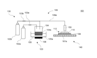
- FIG. 1 is a schematic configuration diagram showing an example of a film forming apparatus of the present invention.
- FIG. It is a figure explaining an example of the misting part which concerns on this invention.
- FIG. 3 is a diagram illustrating an example of a film forming apparatus used in Comparative Example 1;
- FIG. 8 is a diagram illustrating an example of a film forming apparatus used in Comparative Example 2;
- FIG. 10 is a diagram illustrating an example of a film forming apparatus used in Comparative Example 3;
- FIG. 12 is a diagram illustrating an example of a film forming apparatus used in Example 12;
- a film forming apparatus comprising: a gas supply unit; and a film forming unit for heat-treating the mist conveyed by the carrier gas to form a film, wherein the film forming unit includes a film forming chamber and the film forming unit.
- a film having good in-plane uniformity of film thickness is formed by a film forming apparatus in which the height position difference between the inner surface of the ceiling of the film chamber and the substrate mounting surface of the substrate mounting portion is 0.15 cm or more and 6.05 cm or less. was found to be able to form a film, and the present invention was completed.
- the present inventors have also proposed a film formation method for forming a film on a substrate by heat-treating a raw material solution that has been turned into a mist, comprising: A mist transporting step of transporting the mist to a film forming chamber by a carrier gas, and a film forming step of supplying the mist onto the substrate mounted on the substrate mounting part in the film forming chamber, heat-treating the substrate, and forming a film.
- the mist is supplied between the ceiling of the film forming chamber and the substrate from a nozzle provided above the substrate mounting part, and the exhaust gas is discharged from above the substrate in the film forming chamber.
- a film having good in-plane uniformity of film thickness can be formed by a film forming method in which film is formed while supplying the rectified mist onto the substrate by exhausting the mist to the outside of the film forming chamber. I found that I could do it, and completed the present invention.
- the term "mist” as used in the present invention refers to a general term for fine particles of liquid dispersed in gas, and includes what is called fog, liquid droplets, and the like.
- FIG. 1 shows an example of a film forming apparatus 101 according to the present invention.
- the film forming apparatus 101 includes a mist forming unit 120 that forms mist from a raw material solution to generate mist, a carrier gas supply unit 130 that supplies a carrier gas for transporting the mist, and a heat treatment of the mist to form a film on a substrate. It has a film forming section 140 , a transporting section 109 that connects the misting section 120 and the film forming section 140 , transports the mist by a carrier gas, and an exhaust section 170 that exhausts the exhaust gas from the film forming chamber 107 . Further, the operation of the film forming apparatus 101 may be controlled by including a control unit (not shown) that controls the whole or part of the film forming apparatus 101 .
- the mist generating unit 120 mists the raw material solution to generate mist.
- the misting means is not particularly limited as long as it can mist the raw material solution, and may be a known misting means, but it is preferable to use a misting means using ultrasonic vibration. This is because mist can be made more stably.
- misting unit 120 may include a mist generation source 104 containing a raw material solution 104a, a container 105 containing a medium capable of transmitting ultrasonic vibrations, such as water 105a, and an ultrasonic transducer 106 attached to the bottom surface of the container 105.
- a mist generation source 104 which is a container containing a raw material solution 104a, is contained in a container 105 containing water 105a using a support (not shown).
- An ultrasonic transducer 106 is provided at the bottom of the container 105, and the ultrasonic transducer 106 and the oscillator 116 are connected. When the oscillator 116 is operated, the ultrasonic vibrator 106 vibrates, ultrasonic waves propagate through the water 105a into the mist generation source 104, and the raw material solution 104a turns into mist.
- the carrier gas supply unit 130 has a carrier gas source 102a for supplying a carrier gas (main carrier gas), and has a flow control valve 103a for adjusting the flow rate of the main carrier gas sent out from the carrier gas source 102a. good too.
- a carrier gas source 102b for dilution that supplies a carrier gas for dilution (carrier gas for dilution) as needed, and a flow rate for adjusting the flow rate of the carrier gas for dilution sent out from the carrier gas source 102b for dilution
- a control valve 103b may also be provided.
- the type of carrier gas is not particularly limited, and can be appropriately selected according to the film to be deposited. Examples thereof include oxygen, ozone, inert gases such as nitrogen and argon, and reducing gases such as hydrogen gas and forming gas. Also, the number of carrier gases may be one, or two or more. For example, a diluent gas obtained by diluting the same gas as the first carrier gas with another gas (for example, diluted 10 times) may be further used as the second carrier gas, and air may also be used. In addition, the carrier gas may be supplied at two or more locations instead of at one location.
- the film forming section 140 includes a film forming chamber 107 , a substrate mounting portion 112 provided inside the film forming chamber 107 , a nozzle 150 for supplying mist to the inside of the film forming chamber 107 , and an inside of the film forming chamber 107 . and an exhaust portion 170 for exhausting the exhaust gas from.
- the film forming section 140 includes a film forming chamber 107 that partially or entirely surrounds the film forming section 140 .
- the film forming chamber 107 may be formed by enclosing the entire or part of the film forming unit 140 .
- the deposition chamber 107 does not have a completely enclosed shape, but is provided with an exhaust port 111 for exhausting the exhaust gas generated in the deposition chamber. It may have a structure capable of exhausting air.
- the film forming section 140 is equipped with a substrate mounting section 112 on which the substrate 110 is mounted.
- the film forming section 140 can be equipped with a hot plate 108 for heating the placed substrate 110 .
- the hot plate 108 may be provided inside the film forming chamber 107 as shown in FIG. 1 or may be provided outside the film forming chamber 107 .
- the film formation chamber in the present invention includes a bottom wall having a bottom surface parallel to the substrate mounting surface on which the substrate is mounted, and a surface (inner surface of the film forming chamber) that intersects the normal line of the substrate mounting surface. It has a ceiling that is a top wall and side walls that have at least one or more side surfaces (inner surfaces) in contact with the bottom wall.
- the inner surface of the ceiling may be parallel to the substrate mounting surface, and the shape may be a cube, rectangular parallelepiped, or columnar shape having side surfaces orthogonal to the inner surface and the bottom surface of the ceiling. ), and the ceiling and side walls may be integrated.
- the film forming chamber may be formed by setting the structure in advance, or each element constituting the film forming chamber may be made movable so that the shape can be set according to the purpose. It is good as a thing.
- the ceiling in the present invention refers to an upper wall having a surface (also referred to as a "ceiling surface") that intersects with the normal line of the substrate mounting surface of the film forming chamber 107.
- the deposition chamber 107 has an exhaust section 170, and the height difference I [cm] between the substrate mounting surface 113 and the inner surface of the ceiling of the deposition chamber is 0.15 cm or more and 6.05 cm or less. Any length is acceptable, but 0.25 cm or more and 3.05 cm or less is preferable.
- the mist supplied from the nozzle 150 into the film forming chamber 107 passes between the ceiling of the film forming chamber 107, the substrate mounting surface 113 of the substrate mounting part 112, and the substrate 110 on the substrate mounting surface 113,
- the mist is rectified so as to flow in the direction of the exhaust section 170, and the flow speed and direction of the mist can be made uniform.
- the inner surface of the ceiling of the film forming chamber 107 and the substrate mounting surface are preferably parallel. Furthermore, when the substrate is placed on the substrate placement part 112, the height position difference K between the inner surface of the ceiling of the deposition chamber 107 and the surface to be processed of the substrate 110 should be 0.1 cm or more and 6.0 cm or less. is preferable, and 0.2 cm or more and 3.0 cm or less is more preferable. This is because the in-plane uniformity of the film thickness of the film to be formed is further improved.
- the film forming section 140 is provided with a nozzle 150 for supplying mist to the substrate 110 in the film forming chamber 107 above the substrate mounting section 112 .
- the nozzle 150 in the present invention refers to a member for supplying mist into the film forming chamber 107 .
- the supply pipe 109a of the transfer unit 109 which will be described later, may be connected to the film forming chamber 107, and the supply pipe 109a may be used as a nozzle.
- the nozzle 150 includes a connecting portion 151 that connects the conveying portion 109 and the nozzle 150, and a nozzle opening surface (also simply referred to as an opening surface) 152 for ejecting mist.
- the number of nozzles and the number of opening surfaces are not particularly limited as long as they are one or more.
- a plurality of nozzles may be provided as shown in FIG. 5 (nozzle 150a), and a plurality of opening surfaces may be provided as shown in FIG. 6 (nozzle 150b).
- the angle formed by the plane including the nozzle opening surface 152 and the plane including the substrate 110 is not particularly limited.
- a nozzle having an inclined nozzle opening surface may be provided so that the mist can easily flow in a specific direction. However, as shown in FIG. It is preferable that the surface 113 and the nozzle opening surface are provided parallel to each other. This is because a film having better in-plane uniformity of film thickness can be formed with a simpler structure.
- the film forming unit 140 has a position adjusting mechanism (not shown) that can appropriately adjust the height position difference H [cm] between the nozzle opening surface 152 and the surface to be processed of the substrate 110 within a range to be described later. may be provided.
- the ceiling of the film formation chamber 107 has a hole for supplying mist from the nozzle 150 (that is, donut shape), or the film formation chamber 107 has a structure made by combining a plurality of members. It has a structure in which a hole can be formed in the ceiling, and a nozzle is inserted into this hole. If the structure is made by combining a plurality of members, the size of the hole in the ceiling of the film formation chamber 107, the difference H, the difference I, the difference K [cm], and the film formation to be described later can be determined according to the area of the nozzle opening surface. This is preferable because the shortest distance J [cm] between the inner surface of the side wall of the chamber 107 and the substrate mounting area 114 can be appropriately adjusted.
- the height position of the nozzle opening surface may be the same height position as the ceiling of the film formation chamber 107 as shown in FIGS.
- H K as shown in FIGS.
- the nozzle 150 may be constructed by assembling a plurality of members, and by adjusting the size of the members, the area S [cm 2 ] of the opening surface of the nozzle can be appropriately adjusted.
- the area S of the nozzle opening surface 152 is preferably 0.1 or more and 400 cm 2 or less.
- the height position difference H between the nozzle opening surface 152 and the surface to be processed of the substrate 110 is preferably 0.1 cm or more and 6.0 cm or less, more preferably 0.2 or more and 3.0 cm or less. This is because the film to be formed has even better in-plane uniformity of film thickness.
- the area of the nozzle opening surface 152 is S [cm 2 ] and the area of the surface to be processed of the substrate is A [cm 2 ], S/A ⁇ 0.3 is preferable, and 0.004 ⁇ S/A is more preferable. ⁇ 0.15.
- S/A ⁇ 0.3 the film has better in-plane uniformity of film thickness.
- the area A of the substrate is preferably 10 cm 2 or more, more preferably 50 cm 2 or more, and preferably has a diameter of 4 inches (100 mm) or more, and the upper limit is not particularly limited.
- the larger the area of the substrate the larger the area of the film that can be obtained in one film formation, which is suitable for mass production of semiconductor devices.
- the nozzle 150 may be equipped with a temperature adjustment mechanism (not shown) capable of adjusting the temperature of the outer surface of the nozzle 150 and the temperature of the inner surface of the nozzle 150 . If the temperature of the inner and outer surfaces is too high, the evaporation of the mist will be accelerated, resulting in an increase in the film thickness at a position away from the nozzle opening surface on the substrate. The film thickness is reduced at locations near the nozzle opening surface. It is preferable to control the temperature at about 40 to 120°C. The adjustment of H changes the distance from the hot plate 108, and thus the temperature of the nozzle 150 changes. Therefore, it is preferable to provide a temperature control mechanism separate from the hot plate 108 .
- the temperature adjustment mechanism may perform heat exchange using a liquid or gas heat medium, such as by providing a pipe around the nozzle 150, or may apply the Peltier effect. Alternatively, heating by a ribbon heater or the like may be used.
- a heat medium a wide range of known heat mediums can be used. For example, liquid heat mediums such as water, glycols, alcohols, and silicon oils, and gaseous heat mediums such as air, nitrogen, helium, and fluorocarbons are preferably used.
- the shape of the nozzle opening surface 152 is not particularly limited. A polygonal shape, a circular shape, an elliptical shape, etc. are conceivable, but a quadrangular shape is preferable, and a rectangular shape is more preferable.
- L [cm] is the long axis length of the nozzle opening surface 152
- R [cm] is the maximum length of the substrate in the nozzle long axis direction
- L/R ⁇ 1 is good. This is because, if L/R ⁇ 1, a film with good in-plane uniformity of film thickness can be formed on a large-sized substrate.
- the upper limit of L/R is not particularly limited, it is preferably 3 or less because the larger the L/R, the more mist is not supplied to the substrate.
- the angle between the inner surface of the ceiling of the deposition chamber 107 and the substrate 110 and the angle between the inner surface of the ceiling of the deposition chamber 107 and the nozzle opening surface 152 are not particularly limited, but they are preferably parallel. This is because a film having better in-plane uniformity of film thickness can be formed with a simpler structure.
- the shape of the ceiling of the deposition chamber 107 can be tetrahedral, semicircular, circular, or elliptical, but is preferably rectangular or circular. This is because the symmetry is good and the in-plane uniformity of the film thickness of the film to be formed is good.
- a part or the whole of the ceiling of the deposition chamber 107 may be curved or bent so that the mist can easily flow out in a specific direction. preferably placed parallel to the More specifically, the film forming chamber 107 is installed such that the substrate mounting surface 113 of the substrate mounting portion 112 on which the substrate 110 is mounted and the inner surface of the ceiling of the film forming chamber 107 are parallel. is preferred. This is because the formed film has good in-plane uniformity of film thickness.
- the material of the film forming chamber 107 is not particularly limited. Polysulfone, polyethersulfone, polyphenylene sulfide, polyetheretherketone, polyimide, polyetherimide, fluororesin, metals such as iron, aluminum, stainless steel, and gold, quartz, glass, and boron nitride can be considered. It is preferable to use metals such as iron, aluminum, stainless steel, and gold, quartz, boron nitride, and the like, because deformation during heat treatment deteriorates the in-plane uniformity of the film thickness.
- the film formation chamber 107 may be equipped with a temperature control mechanism (not shown) capable of adjusting the temperature of the wall surface of the film formation chamber. If the temperature of the wall surface is too high, the evaporation of the mist will be accelerated, and the film thickness will decrease on the substrate away from the nozzle opening surface. The film thickness decreases at positions close to the upper nozzle opening surface. It is preferable to control the temperature at about 40 to 120°C.
- the substrate mounting part 112 does not have to be provided in the center of the film formation chamber 107 as shown in FIG. It may be different with respect to the inner surface (side surface) of each side wall provided on the front, rear, left, and right.
- the shortest distance between the inner surface of the side wall of the film forming chamber 107 and the substrate mounting area 114 of the substrate mounting part 112 is J [cm].
- the shortest distance J [cm] is not particularly limited, but is preferably 5 cm or less, and may be 0 cm (that is, in contact), but should be 0.5 cm or more and 4 cm or less. is more preferred. If J is within such a range, it is possible to effectively suppress the lateral diffusion of the mist, so the mist is stably supplied to the edge of the substrate 110, and the in-plane uniformity of the film thickness is reduced. In addition, when J is small, it is possible to stably suppress the decrease in the mist supplied at the edge of the substrate due to the friction with the wall surface of the film forming chamber 107, thereby suppressing the decrease in the film thickness.
- the inner surface of the side wall in the present invention means a surface in contact with the bottom surface parallel to the substrate mounting surface of the substrate mounting part 112 of the film formation chamber 107 .
- B/A ⁇ 1 where B [cm 2 ] is the area of the inner surface of the ceiling of the deposition chamber 107 (total area including the nozzle opening surface 152 ), and A [cm 2 ] is the area of the surface to be processed of the substrate.
- 0.0 is preferable, 3.0 or more is preferable, and 5.0 or more is more preferable. This is because the mist flow is less likely to be disturbed by thermal convection in the vicinity of the substrate.
- B is preferably 100 or more. Within these numerical ranges, a film having even better in-plane film thickness uniformity is formed.
- the upper limits of B/A and B are not particularly limited. This is because the rectifying effect of the ceiling of the film formation chamber 107 is exhibited if the value is larger than the above numerical value.
- B/A is preferably 100 or less. This is to prevent the device from becoming unnecessarily large.
- the deposition chamber 107 may be equipped with a temperature control mechanism (not shown) that can control the temperature of the inner surface of the ceiling and the inner surface of the side walls. If the surface temperature is too high, the evaporation of the mist will be accelerated, resulting in an increase in the film thickness on the substrate away from the nozzle opening surface. The film thickness is reduced at locations near the opening surface. It is preferable to control the temperature at about 40 to 120°C.
- the temperature adjustment mechanism may be one that performs heat exchange using a liquid or gas heat medium, one that applies the Peltier effect, or heating by a ribbon heater or the like.
- the heat medium a wide range of known heat mediums can be used. For example, liquid heat mediums such as water, glycols, alcohols, and silicon oils, and gaseous heat mediums such as air, nitrogen, helium, and fluorocarbons are preferably used.
- the film forming section 140 can be provided with a moving mechanism such as a moving stage 161a for moving the substrate 110 below the nozzle 150 as shown in FIG.
- a moving mechanism such as a moving stage 161a for moving the substrate 110 below the nozzle 150 as shown in FIG.
- the direction in which the substrate is moved is not particularly limited.
- FIGS. 9 and 10 show views of the inside of the film forming chamber 107 equipped with a moving mechanism, as viewed from above the substrate mounting portion.
- a moving stage 161a on which the substrate 110 and the hot plate 108 are placed is provided, and the substrate 110 and the hot plate 108 reciprocate under the nozzle 150, as shown in the moving mechanism 160a of FIG.
- the substrate 110 and the hot plate 108 are rotated under the nozzle 150 by a moving stage 161b on which the substrate 110 and the hot plate 108 are placed, as shown in the moving mechanism 160b of FIG.
- a mechanism for rotating the substrate may be provided to rotate the substrate.
- a plurality of substrates 110 and nozzles 150 may be placed on the film forming unit 140 as shown in FIG. 10, or a plurality of substrates may be placed on the film forming unit 140 of FIG.
- films can be formed on many substrates at once while maintaining the in-plane uniformity of the film thickness, so that it is more suitable for mass production.
- the speed at which the substrate is moved and the moving range are not particularly limited.
- 0.5 times or more is preferable, and 1 time or more is more preferable.
- the number of times is set to 0.1 or more, it is possible to prevent the supply gas from being greatly affected by the rising air current accompanying the local evaporation of mist, and the rectification effect of the top plate being difficult to be exhibited. deterioration of uniformity can be more reliably prevented.
- the upper limit of the number of times is not particularly limited, but if the number of times increases, the fixation of the substrate becomes unstable due to inertial force.
- v/D [/min] is 0, where v [mm/min] is the moving speed of the substrate with respect to the width D [mm] of moving the substrate. It is preferably 0.1 or more, preferably 0.5 or more and 120 or less, more preferably 1 to 60. D is not particularly limited. For example, D is preferably the diameter [mm] or more of the substrate (100 or more if the diameter of the substrate is 4 inches), and the upper limit is not particularly limited. If the size is increased, films can be formed on a large number of substrates per nozzle.
- v is not particularly limited. It is preferably 10 mm/min or more and 30000 mm/min, preferably 30 mm/min or more and 12000 mm/min, and more preferably 60 mm/min or more and 6000 mm/min or less.
- the speed is preferably 0.1 rpm or more, preferably 0.5 to 120 rpm, more preferably 1 to 60 rpm.
- the mist supplied together with the carrier gas on the substrate 110 is used for deposition, and the subsequent gas (also referred to as “exhaust gas”) is the mist that is not used for deposition, and the mist that is generated during deposition. gas, carrier gas, etc.) is provided to flow outside the substrate 110 .
- the shape and configuration of the exhaust part 170 are not particularly limited as long as the exhaust part 170 can exhaust the exhaust gas from above the substrate 110 to the outside of the substrate 110 .
- an exhaust port 111 may be provided on the side of the substrate 110 in the deposition chamber 107 to perform forced exhaust.
- a configuration in which the carrier gas or the like supplied between the ceiling of the deposition chamber 107 and the substrate 110 from the nozzle 150 flows to the outside of the substrate 110 is particularly preferable.
- the term "outside of the substrate 110" as used herein refers to the area of the substrate surface excluding the space formed in the normal direction of the surface.
- the exhaust port 111 provided in the film forming chamber 107 can be used as described above, or the exhaust port 111 can be additionally provided with means for forced exhaust. can.
- An example of such an exhaust section 170 is shown in FIG.
- an exhaust unit 172 provided outside the film formation chamber 107 forces the gas in the film formation chamber 107 to exhaust from an exhaust port 111 provided on the side surface of the film formation chamber 107 through an exhaust duct 171.
- the exhaust unit 172 is provided with an exhaust flow control valve 173 for adjusting the exhaust flow rate, so that the exhaust flow rate can be adjusted.
- the substrate 110 A uniform gas flow parallel to the surface of the substrate 110 is generated upwards, allowing a uniform film to be produced on the substrate 110 .
- the shape of the exhaust port 111 is not particularly limited, and may be circular, rectangular, or the like, but preferably has a symmetrical structure perpendicular to the gas flow direction. This is because the symmetry is good and the in-plane uniformity of the film thickness is good.
- the exhaust part 170 may be provided at one place as shown in FIG. 8, or may be provided at two or more places as shown in FIGS. It is preferable that they are provided in a pair of facing directions of the film formation chamber, and more preferably that they are provided so as to be symmetrical with respect to the center of the nozzle opening surface. This is because a film having good in-plane uniformity of film thickness can be formed.
- the exhaust section 170 may be provided with a temperature control mechanism (not shown) for controlling the temperature of a part or the whole thereof in order to suppress the deposition of solids inside the exhaust section.
- a temperature control mechanism suppresses deposition of solids in the exhaust section 170, making it easier to control the exhaust flow rate.
- the temperature adjustment mechanism may be one that performs heat exchange using a liquid or gas heat medium such as by providing a pipe around the exhaust duct 171, or one that applies the Peltier effect. Alternatively, heating by a ribbon heater or the like may be used.
- a heat medium a wide range of known heat mediums can be used. For example, liquid heat mediums such as water, glycols, alcohols, and silicon oils, and gaseous heat mediums such as air, nitrogen, helium, and fluorocarbons are preferably used.
- the material of the member constituting the exhaust part 170 is not particularly limited, and polysulfone, polyethersulfone, polyphenylene sulfide, polyetheretherketone, polyimide, polyetherimide, fluororesin, iron, aluminum, stainless steel, gold, etc. metals, quartz, boron nitride, and the like. It is preferably made of boron nitride. This is because it is possible to suppress non-uniform exhaust gas flow due to rusting and deposition of solids due to unintended reaction with unreacted raw materials.
- the exhaust port 111 (exhaust unit 170) can be moved by providing the exhaust port 111 on the moving mechanisms 160a and 160b. good.
- the conveying section 109 connects the mist forming section 120 and the film forming section 140 . Mist is transported by the carrier gas from the mist generation source 104 of the mist generating unit 120 to the nozzle 150 of the film forming unit 140 via the transport unit 109 .
- the transport section 109 can be, for example, a supply pipe 109a.
- As the supply pipe 109a for example, a quartz pipe or a resin tube can be used.
- the raw material solution 104a is not particularly limited as long as it contains a material that can be misted, and may be an inorganic material or an organic material.
- a metal or metal compound solution (aqueous solution, etc.) is preferably used as the raw material solution, and one or more selected from gallium, iron, indium, aluminum, vanadium, titanium, chromium, rhodium, nickel and cobalt. Anything containing metal can be used.
- the raw material solution contains gallium, a gallium oxide film having good in-plane uniformity of film thickness can be formed.
- the raw material solution is not particularly limited as long as the metal solution can be misted, but as the raw material solution, a metal in the form of a complex or a salt dissolved or dispersed in an organic solvent or water can be preferably used.
- forms of the complex include acetylacetonate complexes, carbonyl complexes, ammine complexes, hydride complexes, and the like.
- Salt forms include, for example, metal chloride salts, metal bromide salts, and metal iodide salts.
- a solution obtained by dissolving the above metal in hydrobromic acid, hydrochloric acid, hydroiodic acid, or the like can also be used as an aqueous salt solution.
- the solute concentration is preferably 0.01 to 1 mol/L.
- the raw material solution may be mixed with additives such as those containing halogen (for example, hydrohalic acid) and oxidizing agents.
- the hydrohalic acid includes, for example, hydrobromic acid, hydrochloric acid, hydroiodic acid, etc. Among them, hydrobromic acid and hydroiodic acid are preferable.
- the oxidizing agent include hydrogen peroxide (H 2 O 2 ), sodium peroxide (Na 2 O 2 ), barium peroxide (BaO 2 ), benzoyl peroxide (C 6 H 5 CO) 2 O 2 and the like.
- Peroxides hypochlorous acid (HClO), perchloric acid, nitric acid, ozone water, organic peroxides such as peracetic acid and nitrobenzene, and the like.
- HCLO hypochlorous acid
- perchloric acid nitric acid
- ozone water organic peroxides such as peracetic acid and nitrobenzene, and the like.
- organic peroxides such as peracetic acid and nitrobenzene, and the like.
- the raw material solution may contain a dopant.
- a dopant is not specifically limited. Examples include n-type dopants such as tin, germanium, silicon, titanium, zirconium, vanadium or niobium, or p-type dopants such as copper, silver, tin, iridium and rhodium.
- the dopant concentration may be, for example, about 1.0 ⁇ 10 ⁇ 9 to 1.0 mol/L, and even at a low concentration of about 1.0 ⁇ 10 ⁇ 7 mol/L or less, about 0.01 mol/L. /L or higher concentration.
- the substrate 110 is not particularly limited as long as it can form a film and can support a film.
- the material of the substrate 110 is also not particularly limited, and a known substrate can be used, and it may be an organic compound or an inorganic compound. Examples include polysulfone, polyethersulfone, polyphenylene sulfide, polyetheretherketone, polyimide, polyetherimide, fluororesin, metals such as iron, aluminum, stainless steel, and gold, quartz, glass, calcium carbonate, gallium oxide, and zinc oxide. etc.
- single crystal substrates such as silicon, sapphire, lithium niobate, lithium tantalate, SiC, GaN, iron oxide, and chromium oxide can be used, and the single crystal substrates described above are desirable in the present invention. With these, a crystalline oxide film of better quality can be obtained.
- sapphire substrates, lithium tantalate substrates, and lithium niobate substrates are relatively inexpensive and industrially advantageous.
- the thickness of the substrate is not particularly limited, but preferably 10 to 2000 ⁇ m, more preferably 50 to 800 ⁇ m.
- Film formation may be performed directly on the substrate, or may be laminated on an intermediate layer formed on the substrate.
- the intermediate layer is not particularly limited, and can be composed mainly of, for example, an oxide containing any one of aluminum, titanium, vanadium, chromium, iron, gallium, rhodium, indium, and iridium.
- the substrate 110 can have a surface area on which a film is formed, for example, of 10 cm 2 or more, more preferably 50 cm 2 or more, or a diameter of 4 inches (100 mm) or more. This is preferable because a film with good in-plane uniformity can be formed over a large area.
- the upper limits of the area and diameter of the substrate are not particularly limited, for example, the area can be 750 cm 2 or the diameter can be 300 mm.
- the raw material solution 104a is accommodated in the mist generation source 104 of the mist generator 120, the substrate 110 such as a crystalline substrate is placed on the hot plate 108, and the hot plate 108 is operated.
- the flow control valves 103a and 103b are opened to supply the main carrier gas from the carrier gas source 102a and the carrier gas for dilution from the carrier gas source 102b for dilution into the film formation chamber 107, and the atmosphere of the film formation chamber 107 is changed to carrier gas. While sufficiently replacing with gas, the flow rate of the main carrier gas and the flow rate of the diluent carrier gas are adjusted and controlled respectively.
- the ultrasonic oscillator 106 is vibrated, and the vibration is propagated to the raw material solution 104a through the water 105a, thereby misting the raw material solution 104a and generating mist.
- the mist is conveyed by the carrier gas from the mist generating section 120 to the film forming section 140 via the conveying section 109 and introduced into the film forming chamber 107 .
- mist is supplied between the ceiling of the film forming chamber 107 and the substrate 110 from the nozzle 150 provided above the substrate mounting part 112 (the hot plate 108 on which the substrate 110 is mounted). Then, the exhaust is rectified by the exhaust from the ceiling of the film formation chamber 107 and the exhaust part 170 (exhaust port 111 and the like) and supplied onto the substrate 110, and is heat-treated by the heat of the hot plate 108 in the film formation chamber 107 and thermally reacts. , is deposited on the substrate 110 .
- the setting is made as described in the above film forming apparatus, and in particular, the height difference between the inner surface of the ceiling of the film forming chamber and the substrate mounting surface of the substrate mounting part is 0.5.
- a film forming apparatus having a film forming chamber set to have a thickness of 15 cm or more and 6.05 cm or less a film having excellent in-plane uniformity of film thickness can be formed. Uniform gas flow along the substrate (parallel to the substrate surface) above the substrate due to the synergistic effect of the rectification effect of the ceiling of the deposition chamber and the convection generated by the supply of mist from the nozzle and the exhaust gas exhaust. is generated, and a uniform film can be formed on the substrate.
- the thermal reaction of the mist in the film forming section 140 is not particularly limited as long as the mist reacts by heating. It can be appropriately set according to the raw material and the film-formed material.
- the heating temperature can be in the range of 120-600°C, preferably in the range of 200-600°C, more preferably in the range of 300-550°C.
- the heating temperature is T [°C]
- the area of the nozzle opening surface 152 is S [cm 2 ]
- the flow rate of the carrier gas is Q [L/min]
- ST/Q is preferably 40 or more, more preferably 100 or more. 2000 or less.
- ST/Q ⁇ 40 the film has better in-plane uniformity of film thickness.
- the thermal reaction may be performed under vacuum, under a non-oxygen atmosphere, under a reducing gas atmosphere, under an air atmosphere, or under an oxygen atmosphere, and may be appropriately set according to the film to be deposited.
- the reaction pressure may be under atmospheric pressure, under increased pressure or under reduced pressure, but film formation under atmospheric pressure is preferable because the apparatus configuration can be simplified.
- the flow rate of the carrier gas is not particularly limited.
- the flow rate is preferably 1 to 80 L/min, more preferably 4 to 40 L/min.
- the flow rate Q of the carrier gas is the value measured at 20°C. can be converted to a volumetric flow rate at
- the flow rate of the exhaust gas is not particularly limited, preferably, when the flow rate of the carrier gas supplied from the nozzle 150 is Q [L/min] and the amount of exhaust gas discharged from the exhaust section 170 is E [L/min], E/Q is preferably 5.0 or less, more preferably 0.5 or more and 3.0 or less. This is because the film has excellent in-plane uniformity of film thickness. Also, at this time, E exhausted from the exhaust part 170 is measured at 20 ° C.
- a linear velocity measured using an anemometer and the area of the opening surface of the exhaust port 111 can be calculated by the product of If the wind speed is measured at other temperatures, or the flow rate is measured by other methods or temperatures, it can be converted to volumetric flow rate at 20° C. using the gas equation of state.
- the area of the nozzle opening surface 152 is S [cm 2 ], the flow rate of the carrier gas is Q [L/min], and the height difference between the nozzle opening surface 152 and the surface to be processed of the substrate 110 (for example, the nozzle opening surface When H [cm] is the longest distance between 152 and the surface of substrate 110, SH/Q is preferably 0.015 or more, preferably 0.1 or more and 20 or less. When SH/Q ⁇ 0.015, the film has better in-plane uniformity of film thickness.
- the velocity of the gas in the direction orthogonal to the substrate on the nozzle opening surface 152 is preferably 0.01 to 8.0 m/s, preferably 0.1 to 2.0 m/s.
- the velocity of the gas in the direction perpendicular to the substrate at the nozzle opening surface 152 is obtained by dividing the carrier gas flow rate Q [L/min] by the area of the nozzle opening surface 152 S [cm 2 ] and converting the units. calculate.
- forming a film while moving the substrate 110 under the nozzle 150 by the moving mechanism 160 is effective in forming a large-area film, and the film thickness distribution is more uniform in the plane and an excellent film can be obtained. is effective for forming a film.
- annealing may be performed after film formation.
- the temperature of the annealing treatment is not particularly limited, but is preferably 600° C. or lower, more preferably 550° C. or lower. This is because the crystallinity of the film is not impaired.
- the annealing treatment time is not particularly limited, but is preferably 10 seconds to 10 hours, more preferably 10 seconds to 1 hour.
- a crystalline oxide film such as a semiconductor film obtained by forming a film by the film forming method according to the present invention is a large-area film with excellent in-plane uniformity of film thickness.
- Example 1 In this example, a film forming apparatus as shown in FIG. 1 was used. A nozzle opening surface 152 is fixed so as to be in the same plane as the ceiling of the film forming chamber 107 .
- B the area of the ceiling
- B 600
- Gallium iodide was added to water and dissolved by stirring at 60°C for 60 minutes to prepare a 0.1 mol/L aqueous solution, which was used as the raw material solution 104a.
- the raw material solution 104 a obtained as described above was accommodated in the mist generation source 104 .
- the temperature of the solution at this time was 25°C.
- a 4-inch (100 mm diameter) c-plane sapphire substrate as the substrate 110 was placed on the hot plate 108 in the deposition chamber 107, and the hot plate 108 was operated to raise the temperature to 500°C.
- the flow control valves 103a and 103b are opened to supply nitrogen gas as a carrier gas into the film forming chamber 107 from the carrier gas source 102a (main carrier gas) and the dilution carrier gas supply source 102b (dilution carrier gas).
- the atmosphere in the film forming chamber 107 was sufficiently replaced with these carrier gases, and the flow rate of the main carrier gas and the diluent carrier gas were adjusted to 12 L/min and 12 L/min, respectively.
- the exhaust flow rate adjustment valve 173 was adjusted so that the exhaust amount E [L/min] at the exhaust port 111 was 24. At this time, E/Q was 1.0.
- the ultrasonic oscillator 106 was vibrated at 2.4 MHz, and the vibration was propagated through the water 105a to the raw material solution 104a, thereby misting the raw material solution 104a to generate mist.
- This mist was supplied to the substrate 110 through the supply pipe 109a and the nozzle 150 by carrier gas.
- a nozzle having a rectangular nozzle opening surface 152 is used as the nozzle 150.
- the mist is thermally reacted in the deposition chamber 107 while the exhaust gas is exhausted from the exhaust port 111, so that the gallium oxide ( ⁇ -Ga) having a corundum structure is formed on the substrate 110 2 O 3 ) was formed.
- the film formation time was 300 minutes.
- a moving stage 161a as shown in FIG. 13 reciprocated the substrate and hot plate at a speed of 15 [cm/min] so as to pass under the nozzle once per minute.
- Example 1 The procedure was the same as in Example 1, except that a film forming apparatus without a film forming chamber 107 as shown in FIG. 12 was used and the film forming time was set to 60 minutes.
- Example 2 The area S of the nozzle opening surface 152 is 2.4 [cm 2 ], the height difference H [cm] between the nozzle opening surface 152 and the substrate 110 is 6.0 [cm], the ceiling of the film forming chamber 107 and the substrate
- the height position difference I between the mounting portion 112 and the substrate mounting surface 113 was changed to 6.05 [cm]
- the flow rate Q of the carrier gas was changed to 48 [L/min]
- SH/Q was changed to 0.3
- Example 3 The area S of the nozzle opening surface 152 is 12 [cm 2 ], the height difference H [cm] between the nozzle opening surface 152 and the substrate 110 is 0.1 [cm], and the ceiling of the deposition chamber 107 and the substrate placement
- the height position difference I between the portion 112 and the substrate mounting surface 113 is changed to 0.15 [cm]
- the flow rate Q of the carrier gas is changed to 12 [L/min]
- the exhaust amount E is changed to 12 [L/min].
- SH/Q 0.1
- ST/Q 500
- Example 5 The shortest distance J [cm] between the substrate mounting area 114 and the inner surface of the side wall of the deposition chamber 107 is set to 5.0 [cm], and the area B [cm 2 ] of the ceiling of the deposition chamber 107 is set to 800 [cm 2 ]. Film formation was carried out in the same manner as in Example 1, except that B/A was changed to 10.2 and the film formation time was set to 240 minutes.
- Example 7 Film formation was carried out in the same manner as in Example 1, except that the exhaust amount E was changed to 120 [L/min], E/Q was set to 5.0, and the film formation time was set to 360 minutes.
- Example 8 Film formation was performed in the same manner as in Example 1, except that the exhaust amount E was changed to 360 [L/min], E/Q was set to 15.0, and the film formation time was set to 60 minutes.
- Example 9 A 6-inch (150 mm diameter) c-plane sapphire substrate was used as the substrate 110, the flow rate Q of the carrier gas was 36 [L/min], the exhaust amount E was 36 [L/min], and the major axis of the nozzle opening surface 152.
- the length L [cm] is 18 [cm]
- the area S of the nozzle opening surface 152 is 9.0 [cm 2 ]
- the area A of the substrate 110 is 176.7 [cm 2 ]
- S/A is 0.051.
- B/A 3.4
- the film formation time was set to 180 minutes.
- Example 11 A 0.1 mol/L solution was prepared by dissolving an aluminum acetylacetonate complex in a hydrochloric acid solution and used as a raw material solution.
- the height position difference I from the substrate mounting surface of 112 was changed to 3.05 [cm]
- the film formation temperature T [° C.] was changed to 550 [° C.]
- ST/Q was set to 137.5.
- Film formation was performed in the same manner as in Example 1, except that the film formation time was 60 minutes.
- Example 12 Dissolving gallium nitrate in water to prepare a 0.1 mol/L solution and using it as a raw material solution, using a film forming apparatus as shown in FIG. Film formation was performed in the same manner as in Example 1, except that the substrate was not moved and the film formation time was set to 60 minutes.
- a substrate mounting for mounting a substrate is provided in the film forming unit and includes a misting unit, a carrier gas supply unit, a film forming unit, and an exhaust unit.
- a nozzle for supplying mist onto the substrate and a film forming chamber containing the substrate mounting portion are provided above the portion, and the height difference between the inner surface of the ceiling of the film forming chamber and the substrate mounting portion is set to zero. It was found that by using a film forming apparatus in which a film forming chamber is set to have a thickness of 0.15 cm or more and 6.05 cm or less, a film having excellent in-plane uniformity of film thickness can be obtained.
- Patent Document 5 Due to the difference in the substrate installation method and the presence or absence of a mechanism for rectifying mist between Patent Document 5 and the film forming apparatus and film forming method according to the present invention, the 4 described in Patent Document 5 It is presumed that in the example of forming a film on a substrate of inches or more, a film with good in-plane uniformity of film thickness could not be obtained.
- the present invention is not limited to the above embodiments.
- the above-described embodiment is an example, and any device having substantially the same configuration as the technical idea described in the claims of the present invention and exhibiting the same effect is the present invention. included in the technical scope of
Landscapes
- Chemical & Material Sciences (AREA)
- General Chemical & Material Sciences (AREA)
- Chemical Kinetics & Catalysis (AREA)
- Engineering & Computer Science (AREA)
- Materials Engineering (AREA)
- Metallurgy (AREA)
- Organic Chemistry (AREA)
- Mechanical Engineering (AREA)
- Inorganic Chemistry (AREA)
- Dispersion Chemistry (AREA)
- Crystallography & Structural Chemistry (AREA)
- Chemically Coating (AREA)
Priority Applications (5)
| Application Number | Priority Date | Filing Date | Title |
|---|---|---|---|
| CN202280068535.5A CN118103547A (zh) | 2021-10-14 | 2022-06-29 | 成膜装置及制造方法 |
| JP2023554260A JPWO2023062889A1 (https=) | 2021-10-14 | 2022-06-29 | |
| EP22880594.1A EP4417732A1 (en) | 2021-10-14 | 2022-06-29 | Film deposition device and manufacturing method |
| KR1020247011983A KR20240074787A (ko) | 2021-10-14 | 2022-06-29 | 성막 장치 및 제조 방법 |
| US18/700,338 US20240401195A1 (en) | 2021-10-14 | 2022-06-29 | Film-forming apparatus and manufacturing method |
Applications Claiming Priority (2)
| Application Number | Priority Date | Filing Date | Title |
|---|---|---|---|
| JP2021-168663 | 2021-10-14 | ||
| JP2021168663 | 2021-10-14 |
Publications (1)
| Publication Number | Publication Date |
|---|---|
| WO2023062889A1 true WO2023062889A1 (ja) | 2023-04-20 |
Family
ID=85988244
Family Applications (1)
| Application Number | Title | Priority Date | Filing Date |
|---|---|---|---|
| PCT/JP2022/025998 Ceased WO2023062889A1 (ja) | 2021-10-14 | 2022-06-29 | 成膜装置及び製造方法 |
Country Status (7)
| Country | Link |
|---|---|
| US (1) | US20240401195A1 (https=) |
| EP (1) | EP4417732A1 (https=) |
| JP (1) | JPWO2023062889A1 (https=) |
| KR (1) | KR20240074787A (https=) |
| CN (1) | CN118103547A (https=) |
| TW (1) | TW202316499A (https=) |
| WO (1) | WO2023062889A1 (https=) |
Cited By (2)
| Publication number | Priority date | Publication date | Assignee | Title |
|---|---|---|---|---|
| JPWO2023079787A1 (https=) * | 2021-11-02 | 2023-05-11 | ||
| JP7731648B1 (ja) * | 2024-03-06 | 2025-09-01 | 株式会社Tmeic | 基材表面処理装置 |
Citations (10)
| Publication number | Priority date | Publication date | Assignee | Title |
|---|---|---|---|---|
| JPH01257337A (ja) | 1988-04-06 | 1989-10-13 | Fujitsu Ltd | 気相エピタキシャル成長装置 |
| JPH11111706A (ja) * | 1997-10-06 | 1999-04-23 | Ebara Corp | 原料供給装置 |
| JP2005307238A (ja) | 2004-04-19 | 2005-11-04 | Shizuo Fujita | 成膜方法及び成膜装置 |
| JP2012046772A (ja) | 2010-08-24 | 2012-03-08 | Sharp Corp | ミストcvd装置及びミスト発生方法 |
| JP5397794B1 (ja) | 2013-06-04 | 2014-01-22 | Roca株式会社 | 酸化物結晶薄膜の製造方法 |
| JP2014063973A (ja) * | 2012-08-26 | 2014-04-10 | Kumamoto Univ | 酸化亜鉛結晶層の製造方法及び酸化亜鉛結晶層並びにミスト化学気相成長装置 |
| JP2017020076A (ja) * | 2015-07-10 | 2017-01-26 | 東芝三菱電機産業システム株式会社 | 成膜装置及び成膜方法 |
| JP2020098846A (ja) * | 2018-12-18 | 2020-06-25 | 信越化学工業株式会社 | 酸化ガリウム膜の製造方法 |
| WO2020261355A1 (ja) | 2019-06-25 | 2020-12-30 | 日本碍子株式会社 | 半導体膜 |
| JP6925548B1 (ja) * | 2020-07-08 | 2021-08-25 | 信越化学工業株式会社 | 酸化ガリウム半導体膜の製造方法及び成膜装置 |
Family Cites Families (1)
| Publication number | Priority date | Publication date | Assignee | Title |
|---|---|---|---|---|
| JPS5397794U (https=) | 1977-01-12 | 1978-08-08 |
-
2022
- 2022-06-29 EP EP22880594.1A patent/EP4417732A1/en active Pending
- 2022-06-29 WO PCT/JP2022/025998 patent/WO2023062889A1/ja not_active Ceased
- 2022-06-29 JP JP2023554260A patent/JPWO2023062889A1/ja active Pending
- 2022-06-29 CN CN202280068535.5A patent/CN118103547A/zh active Pending
- 2022-06-29 KR KR1020247011983A patent/KR20240074787A/ko active Pending
- 2022-06-29 US US18/700,338 patent/US20240401195A1/en active Pending
- 2022-07-05 TW TW111125084A patent/TW202316499A/zh unknown
Patent Citations (10)
| Publication number | Priority date | Publication date | Assignee | Title |
|---|---|---|---|---|
| JPH01257337A (ja) | 1988-04-06 | 1989-10-13 | Fujitsu Ltd | 気相エピタキシャル成長装置 |
| JPH11111706A (ja) * | 1997-10-06 | 1999-04-23 | Ebara Corp | 原料供給装置 |
| JP2005307238A (ja) | 2004-04-19 | 2005-11-04 | Shizuo Fujita | 成膜方法及び成膜装置 |
| JP2012046772A (ja) | 2010-08-24 | 2012-03-08 | Sharp Corp | ミストcvd装置及びミスト発生方法 |
| JP2014063973A (ja) * | 2012-08-26 | 2014-04-10 | Kumamoto Univ | 酸化亜鉛結晶層の製造方法及び酸化亜鉛結晶層並びにミスト化学気相成長装置 |
| JP5397794B1 (ja) | 2013-06-04 | 2014-01-22 | Roca株式会社 | 酸化物結晶薄膜の製造方法 |
| JP2017020076A (ja) * | 2015-07-10 | 2017-01-26 | 東芝三菱電機産業システム株式会社 | 成膜装置及び成膜方法 |
| JP2020098846A (ja) * | 2018-12-18 | 2020-06-25 | 信越化学工業株式会社 | 酸化ガリウム膜の製造方法 |
| WO2020261355A1 (ja) | 2019-06-25 | 2020-12-30 | 日本碍子株式会社 | 半導体膜 |
| JP6925548B1 (ja) * | 2020-07-08 | 2021-08-25 | 信越化学工業株式会社 | 酸化ガリウム半導体膜の製造方法及び成膜装置 |
Cited By (4)
| Publication number | Priority date | Publication date | Assignee | Title |
|---|---|---|---|---|
| JPWO2023079787A1 (https=) * | 2021-11-02 | 2023-05-11 | ||
| JP7762218B2 (ja) | 2021-11-02 | 2025-10-29 | 信越化学工業株式会社 | 成膜装置及び成膜方法並びに積層体 |
| JP7731648B1 (ja) * | 2024-03-06 | 2025-09-01 | 株式会社Tmeic | 基材表面処理装置 |
| WO2025186929A1 (ja) * | 2024-03-06 | 2025-09-12 | 株式会社Tmeic | 基材表面処理装置 |
Also Published As
| Publication number | Publication date |
|---|---|
| US20240401195A1 (en) | 2024-12-05 |
| EP4417732A1 (en) | 2024-08-21 |
| JPWO2023062889A1 (https=) | 2023-04-20 |
| CN118103547A (zh) | 2024-05-28 |
| TW202316499A (zh) | 2023-04-16 |
| KR20240074787A (ko) | 2024-05-28 |
Similar Documents
| Publication | Publication Date | Title |
|---|---|---|
| JP7234310B2 (ja) | 酸化ガリウム半導体膜の製造方法及び成膜装置 | |
| JP7223515B2 (ja) | 成膜装置及び成膜方法 | |
| WO2020129625A1 (ja) | 酸化ガリウム膜の製造方法 | |
| JP2022119880A (ja) | 成膜装置及び成膜方法 | |
| JP7803500B2 (ja) | 酸化ガリウム半導体膜の製造方法 | |
| JP7731969B2 (ja) | 成膜装置、成膜方法、酸化ガリウム膜および積層体 | |
| WO2023062889A1 (ja) | 成膜装置及び製造方法 | |
| JP2023030097A (ja) | 結晶性酸化物薄膜 | |
| JP2023106479A (ja) | 成膜装置及び成膜方法 | |
| JP7265517B2 (ja) | 成膜方法 | |
| JP7436333B2 (ja) | 成膜方法及び成膜装置 | |
| WO2022191230A1 (ja) | 酸化物半導体膜およびその成膜方法、半導体装置 | |
| US20240425982A1 (en) | Film forming apparatus and film forming method, and oxide semiconductor film and laminate | |
| JP7274024B2 (ja) | 成膜装置 | |
| TW202338143A (zh) | 成膜方法 | |
| JP7313530B2 (ja) | 成膜方法 | |
| JP7610231B2 (ja) | 原料溶液の製造方法、成膜方法及び製品ロット | |
| TW202405226A (zh) | 成膜方法及成膜裝置 |
Legal Events
| Date | Code | Title | Description |
|---|---|---|---|
| 121 | Ep: the epo has been informed by wipo that ep was designated in this application |
Ref document number: 22880594 Country of ref document: EP Kind code of ref document: A1 |
|
| ENP | Entry into the national phase |
Ref document number: 2023554260 Country of ref document: JP Kind code of ref document: A |
|
| WWE | Wipo information: entry into national phase |
Ref document number: 202280068535.5 Country of ref document: CN Ref document number: 202447029070 Country of ref document: IN |
|
| ENP | Entry into the national phase |
Ref document number: 20247011983 Country of ref document: KR Kind code of ref document: A |
|
| WWE | Wipo information: entry into national phase |
Ref document number: 2022880594 Country of ref document: EP |
|
| NENP | Non-entry into the national phase |
Ref country code: DE |
|
| ENP | Entry into the national phase |
Ref document number: 2022880594 Country of ref document: EP Effective date: 20240514 |