WO2023058668A1 - 光通信システム - Google Patents
光通信システム Download PDFInfo
- Publication number
- WO2023058668A1 WO2023058668A1 PCT/JP2022/037202 JP2022037202W WO2023058668A1 WO 2023058668 A1 WO2023058668 A1 WO 2023058668A1 JP 2022037202 W JP2022037202 W JP 2022037202W WO 2023058668 A1 WO2023058668 A1 WO 2023058668A1
- Authority
- WO
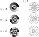
- WIPO (PCT)
- Prior art keywords
- liquid crystal
- optical
- phase
- polarized light
- pattern
- Prior art date
- Legal status (The legal status is an assumption and is not a legal conclusion. Google has not performed a legal analysis and makes no representation as to the accuracy of the status listed.)
- Ceased
Links
Images






Classifications
-
- G—PHYSICS
- G02—OPTICS
- G02B—OPTICAL ELEMENTS, SYSTEMS OR APPARATUS
- G02B5/00—Optical elements other than lenses
- G02B5/30—Polarising elements
-
- G—PHYSICS
- G02—OPTICS
- G02B—OPTICAL ELEMENTS, SYSTEMS OR APPARATUS
- G02B5/00—Optical elements other than lenses
- G02B5/30—Polarising elements
- G02B5/3083—Birefringent or phase retarding elements
-
- H—ELECTRICITY
- H04—ELECTRIC COMMUNICATION TECHNIQUE
- H04B—TRANSMISSION
- H04B10/00—Transmission systems employing electromagnetic waves other than radio-waves, e.g. infrared, visible or ultraviolet light, or employing corpuscular radiation, e.g. quantum communication
- H04B10/50—Transmitters
- H04B10/516—Details of coding or modulation
- H04B10/532—Polarisation modulation
-
- H—ELECTRICITY
- H04—ELECTRIC COMMUNICATION TECHNIQUE
- H04J—MULTIPLEX COMMUNICATION
- H04J14/00—Optical multiplex systems
- H04J14/05—Spatial multiplexing systems
-
- H—ELECTRICITY
- H04—ELECTRIC COMMUNICATION TECHNIQUE
- H04J—MULTIPLEX COMMUNICATION
- H04J14/00—Optical multiplex systems
- H04J14/06—Polarisation multiplex systems
Definitions
- the present invention relates to optical communication systems.
- the amount of communication on the Internet is increasing year by year, and there is a demand for increased capacity in the optical communication system, which is the backbone network.
- Non-Patent Document 1 proposes an optical communication system using 15 different modes of light.
- an object of the present invention is to provide a multiplex optical communication system with a simple optical system and high efficiency.
- a patterned retardation plate is applied, and a plurality of incident light beams or expanded incident light passes through the patterned retardation plate only once, thereby generating a plurality of different modes. It was found that by adopting a configuration that converts light into an optical vortex, it is possible to provide a multiplex optical communication system with a simple optical system and high efficiency.
- an optical transmitter ; a transmission line; including an optical receiver, An optical communication system, wherein the optical transmitter includes a polarized light source, a patterned retardation plate that converts light from the polarized light source into a plurality of optical vortices, a modulator, and a multiplexer.
- the optical transmitter includes a polarized light source, a patterned retardation plate that converts light from the polarized light source into a plurality of optical vortices, a modulator, and a multiplexer.
- a plurality of polarized light sources or a single polarized light source is distributed by widening, and a modulator is included between the patterned retardation plate and the multiplexer.
- a modulator is included between the patterned retardation plate and the multiplexer.
- the patterned retardation plate includes those in which the azimuth angle of the slow axis changes continuously by ⁇ ⁇ 180° ( ⁇ is an integer) when making one turn around a certain point [1] ⁇
- [6] further including a polarizing plate, The optical communication system according to any one of [1] to [5], wherein the polarizing plate and the patterned retardation plate are integrated.
- the optical communication system according to any one of [1] to [6], comprising an alignment mechanism capable of accurately aligning the center of the patterned retardation plate and the incident position of light.
- the patterned retardation plate has a plurality of retardation patterns different in at least one of the order and the number of nodes in the same plane.
- a patterned retardation plate having a plurality of retardation patterns different in at least one of the order and the number of nodes in the same plane.
- FIG. 1 is a conceptual diagram of an optical communication system 1 according to Embodiment 1.
- FIG. FIG. 4 is a schematic diagram of the slow axis distribution of the phase difference pattern used in the present invention.
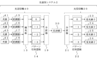
- 2 is a conceptual diagram of an optical communication system 2 according to Embodiment 2.
- FIG. It is a figure for demonstrating the relationship between the phase of a retardation pattern, and the direction of a liquid crystal compound.
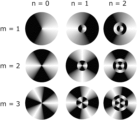
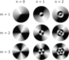
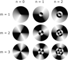
- FIG. 2 is a conceptual diagram showing an example of a phase difference pattern used in the present invention in terms of phase distribution; It is the figure which represented each phase difference pattern with phase distribution, and the figure which represented each phase difference pattern with slow-axis distribution. It is the figure which represented each phase difference pattern with phase distribution, and the figure which represented each phase difference pattern with slow-axis distribution.
- FIG. 4 is a conceptual diagram showing another example of the phase difference pattern used in the present invention in terms of phase distribution
- FIG. 2 is a conceptual diagram of an exposure mask used when producing a retardation pattern used in the present invention, and a diagram showing the polarization direction of light for exposure.
- FIG. 2 is a conceptual diagram of an exposure mask used when producing a retardation pattern used in the present invention, and a diagram showing the polarization direction of light for exposure.
- FIG. 2 is a conceptual diagram of an exposure mask used when producing a retardation pattern used in the present invention, and a diagram showing the polarization direction of light for exposure.
- FIG. 2 is a conceptual diagram of an exposure mask used when producing each phase difference pattern
- FIG. 2 is a conceptual diagram of an exposure mask used when producing each phase difference pattern
- FIG. 2 is a conceptual diagram of an exposure mask used when producing each phase difference pattern;
- FIG. 1 is a conceptual diagram showing the configuration of an optical communication system 1 according to Embodiment 1 of the present invention.
- An optical communication system 1 connects an optical transmitter 10 that transmits a plurality of signal lights, an optical receiver 20 that receives a plurality of signal lights transmitted from the optical transmitter 10, and the optical transmitter 10 and the optical receiver 20. It has a transmission line 30 that
- the optical transmitter 10 has a light source 11 , a beam spreading element 12 , a polarizing plate 13 , a patterned retardation plate 14 , modulators 15 to 18 and a multiplexer 19 .
- the light source 11 must be a polarized light source, but the light source itself may emit polarized light, or the light source may have a polarizing plate.
- the light emitted from the light source 11 is preferably near-infrared light. Near-infrared light is light in the wavelength range of 700 nm to 2500 nm.
- a light emitting diode (LED), a laser light source, or the like can be used as the light source 11 .
- the light emitted from the light source 11 enters the beam expanding element 12 and is expanded in the horizontal direction.
- a cylindrical lens, a microlens (combination of a convex lens and a concave lens), or the like can be used as the beam expanding element 12 .
- the widened light enters the polarizing plate 13 and is converted into linearly polarized light.
- the polarizing plate 13 is not particularly limited as long as it has a degree of polarization corresponding to the wavelength of the light source 11, and either an absorption type or a reflection type can be used.
- each light is divided into optical vortices with different spiral directions and pitches of the spiral structure and superimposed.
- the linearly polarized light enters the pattern retardation plate 14 and is converted into optical vortices corresponding to each order.
- the pattern retardation plate 14 has a plurality of retardation patterns for converting incident linearly polarized light into optical vortices.
- the number of retardation patterns that the patterned retardation plate has may be 2 to 3, or may be 5 or more. That is, the number of m can be adjusted as needed.
- Each phase difference pattern preferably has a configuration in which the azimuth angle of the slow axis in the plane changes discretely or continuously in the circumferential direction around one point, and in particular, the azimuth angle of the slow axis is More preferably, it changes discretely or continuously by ⁇ 180° ( ⁇ is an integer) when making one turn around one point.
- ⁇ is an integer
- m +1
- the direction of the slow axis changes counterclockwise (counterclockwise) by 180° when one rotation is made counterclockwise about the central point. becomes.
- the phase difference between the patterned retardation plate 14 and the patterned retardation plate 22 is preferably ⁇ /2 with respect to the wavelength ⁇ of the incident light.
- the retardation patterns of the patterned retardation plates 14 and 22 can be produced by a known method. As a specific example, it can be produced by the method described in JP-A-2008-233903.
- the polarizing plate 13 and the pattern retardation plate 14 may be integrated.
- a known bonding method such as an adhesive and/or an adhesive may be used.
- the integration has the advantage of reducing the loss of light due to reflection on the air interface and simplifying the assembly because the number of parts is reduced.
- the pattern retardation plate 14 and the pattern retardation plate 22, which will be described later, preferably have an alignment mechanism capable of accurately aligning the incident position of the incident light with the center of each retardation pattern. By precisely aligning the incident position of the incident light with the center of each phase difference pattern, the conversion efficiency can be maximized and the S/N ratio of communication is improved.
- a plurality of optical vortices generated by passing through each phase difference pattern are incident on modulators 15 to 18, respectively.
- the modulators 15 to 18 modulate the amplitude of the incident optical vortex.
- the amplitude of each optical vortex is modulated by the modulators 15 to 18 only for the optical vortex of the order corresponding to the required signal.
- Amplitude modulation may be two-step digital modulation or multi-step modulation.
- the modulators 15 to 18 for example, MEMS (Micro-Electro-Mechanical Systems) mirrors and LCOS (Liquid Crystal On Silicon) elements can be used.
- a different signal is assigned to each optical vortex by the modulators 15-18.
- the optical vortices modulated by the modulators 15 to 18 are multiplexed by the multiplexer 19 and transmitted to the transmission line 30 .
- the multiplexer 19 is not limited, and various known multiplexers can be used.
- Transmission line 30 may be free space, but is preferably optical fiber for S/N ratio and stability.
- the optical fiber is not particularly limited, and any optical fiber generally used in optical communication systems can be used.
- optical receiver 20 constituting the optical communication system of the present invention
- a known receiver for optical vortex can be applied. That is, it is sufficient that the signal can be reproduced from the amplitude of each channel after demultiplexing the optical vortex with an appropriate demultiplexer.
- FIG. 1 The configuration shown in FIG. 1 is a preferred example of the optical receiver 20.
- FIG. The optical receiver 20 has a demultiplexer 21, a pattern phase difference plate 22, and light receiving elements 23-26.
- the transmitted optical signal (multiplexed optical vortex) is demultiplexed by the demultiplexer 21 so that it can be incident on each phase difference pattern of the pattern phase difference plate 22 .
- the pattern retardation plate 22 has the same order as the phase difference pattern of the pattern retardation plate 14, but has the same absolute value but a different sign.
- an optical signal is incident on a phase difference pattern with the same absolute value as the order of the optical vortex that has passed through the modulators 15 to 18 but with a different sign, the 0th-order light with the maximum optical intensity at the central portion is generated.
- zero-order light is not generated, and the donut-shaped light intensity distribution of the light vortex is maintained, so the light intensity becomes 0 at the central portion. That is, each phase difference pattern of the patterned phase difference plate 22 intensifies only the light intensity of the central portion of the light vortex of the corresponding order.
- each phase difference pattern of the pattern phase difference plate 22 is received by the light receiving elements 23 to 26, and if the light intensity of the central portion is measured, an optical signal corresponding to the order of the optical vortex passed by the optical transmitter 10 is obtained. is detected. Thereby, the signal assigned to each optical vortex can be detected.
- the optical system is simple and highly efficient multiplex optical communication is possible by using the optical vortex generated by the phase difference pattern.
- FIG. 3 is a conceptual diagram showing the configuration of an optical communication system 2 according to Embodiment 2 of the present invention.
- the optical transmitter 40 has light sources 41 to 44 consisting of a plurality of light sources, that there is no beam spreading element 12, and that the modulators 15 to 18 are the light sources 41 to 44 and the polarizing plate 13. It differs from the first embodiment in that it is arranged between them. Except for this point, the second embodiment is the same as the first embodiment.
- the optical transmitter 40 has light sources 41 - 44 , modulators 15 - 18 , a polarizing plate 13 , a pattern retardation plate 14 and a multiplexer 16 .
- the light sources 41 to 44 are arranged in the same number as the number of the phase difference patterns arranged on the pattern retardation plate 14. By turning ON/OFF the light sources 41 to 44 or applying modulation by the modulators 15 to 18, Signal can be switched.
- the light sources 41 to 44 are not particularly limited, and light sources generally used in optical communication systems can be used, but near-infrared light is preferred.
- the lights emitted from the light sources 41 to 44 enter the polarizing plate 13 and are converted into linearly polarized light, enter the phase difference patterns of each order on the pattern phase difference plate 14 , and generate optical vortices of each order. integrated with.
- the subsequent transmission line 30 and optical receiver 20 are the same as in the first embodiment.
- the optical system is simple and highly efficient multiplex optical communication is possible by using the optical vortex generated by the phase difference pattern.
- the optical communication system 2 is configured to have the modulators 15 to 18 between the light sources 41 to 44 and the polarizing plate 13, but is not limited to this. and the multiplexer 19, the modulators 15 to 18 may be provided.
- the patterned retardation plate has a configuration in which a plurality of retardation patterns are arranged in one direction, but the pattern is not limited to this, and may be arranged two-dimensionally.
- the beam expanding element may expand the light in two orthogonal directions, or a plurality of light sources may be arranged in two directions according to the arrangement of the phase difference patterns. May be ordered in dimension order.
- a plurality of light sources may be arranged in one direction, and the light emitted from each light source may be widened by a plurality of beam widening elements in a direction perpendicular to the arrangement direction of the light sources.
- the retardation pattern of the patterned retardation plate of the optical communication system of the present invention will be described in more detail below.
- the patterned retardation plate is preferably a liquid crystal layer formed using a composition containing a liquid crystal compound, and each retardation pattern is such that the optic axis derived from the liquid crystal compound is oriented in a pattern described later. is preferred.
- FIG. 4 is a diagram showing the relationship between the orientation of the optical axis and the normalized phase for each minute area.
- FIG. 4 shows the direction of the optical axis (slow axis) of each minute region in the phase difference pattern as a normalized phase from 0 to 2 ⁇ , visualized in a gray scale with 0 being black and 2 ⁇ being white. is.
- Reference numeral 50 in FIG. 4 represents (orientation of the optical axis of) the liquid crystal compound.
- phase 1 the state in which the optical axis 50 faces the horizontal direction in the figure (the angle of the optical axis in the polar coordinate display is 0°) is defined as phase 0.
- a state in which the optical axis 50 is rotated counterclockwise by 180° is defined as a phase 2 ⁇ , and the phase is normalized according to the counterclockwise rotation angle.
- the phase is ⁇ /2 when the optical axis 50 is rotated counterclockwise by 45° (the second optical axis 50 from the left), and the phase is ⁇ /2 when the optical axis 50 is rotated by 90° (the third optical axis 50 from the left).
- the 135° rotated state (second optical axis 50 from the right) has a phase of 3 ⁇ /2.
- the change in the optical axis 50 is actually a continuous change, and the optical axis (liquid crystal compound) 50 oriented at an angle therebetween exists between the optical axes 50 in FIG.
- the states of the optical axes of phase 0 and phase 2 ⁇ are the same.
- the phase of the phase difference pattern is represented in grayscale, and the orientation of the optical axis 50 is superimposed.
- the direction of the optic axis 50 in minute regions in the liquid crystal layer is the direction of the optic axis derived from the liquid crystal compound. Therefore, the optical axis 50 in FIG. 5 can also be said to be the optical axis of the liquid crystal compound.
- the liquid crystal compound is a rod-like liquid crystal compound
- the long axis of the rod-like liquid crystal compound is the optical axis derived from the liquid crystal compound.
- the axis perpendicular to the discotic surface of the discotic liquid crystal compound is the optical axis.
- the direction of the optic axis (liquid crystal compound) 50 in the minute area rotates counterclockwise when viewed counterclockwise in the circumferential direction.
- the optical axis 50 rotates by half (180°) during one turn in the circumferential direction from the position where the phase is 0, that is, the phase gradually changes from 0 to 2 ⁇ .
- the direction of the optical axis (liquid crystal compound) 50 in the minute area is counterclockwise.
- the optical axis 50 rotates once in the circumferential direction from the position where the phase is 0, and the optical axis 50 rotates once (360°), that is, the phase repeats the phase change from 0 to 2 ⁇ twice.
- the direction of the optical axis (liquid crystal compound) 50 in the minute area is counterclockwise. While rotating, the optical axis 50 rotates once and a half (540°) during one turn in the circumferential direction from the position where the phase is 0, that is, the phase repeats the phase change from 0 to 2 ⁇ three times. .
- examples of retardation patterns possessed by patterned retardation layers are represented by phases (gray scale) normalized from 0 to 2 ⁇ .
- the phase difference pattern has a phase that changes in the circumferential direction and a constant phase in the radial direction, but is not limited to this.
- the retardation pattern of the patterned retardation layer may have nodes with discontinuous phases in the radial direction.
- FIG. 6 shows another example of the retardation pattern possessed by the patterned retardation layer.
- the diagram on the left side is a diagram showing the phase difference pattern
- the diagram on the right side is a schematic diagram of the slow axis distribution of the phase difference pattern.
- the phase when viewed counterclockwise in the circumferential direction, gradually changes from 0 to 2 ⁇ during one turn in the circumferential direction from the position where the phase is 0.
- the position of the phase 0 in the circumferential direction is shifted by 90° between the circular area and the annular area.
- the position of the phase 0 in the circumferential direction is shifted by 60° between the circular area and the annular area.
- the patterned retardation plate of the optical communication system of the present invention may include a retardation pattern having nodes.
- the phase gradually changes from 0 to 2 ⁇ during one turn in the circumferential direction from the position where the phase is 0. .
- the position of the phase 0 in the circumferential direction is shifted by 180° between the circular area and the first annular area.
- the position of the phase 0 in the circumferential direction is shifted by 180° between the first annular region and the second annular region. In other words, the non-adjacent circular region and the second annular region coincide in the position where the phase is 0 in the circumferential direction.
- the position of the phase 0 in the circumferential direction is shifted by 90° between the circular region and the first annular region.
- the position of the phase 0 in the circumferential direction is shifted by 90° between the first annular region and the second annular region. In other words, the non-adjacent circular region and the second annular region coincide in the position where the phase is 0 in the circumferential direction.
- the position of the phase 0 in the circumferential direction is shifted by 60° between the circular area and the first annular area.
- the position of the phase 0 in the circumferential direction is shifted by 60° between the first annular region and the second annular region. In other words, the non-adjacent circular region and the second annular region coincide in the position where the phase is 0 in the circumferential direction.
- the patterned retardation plate of the optical communication system of the present invention may include retardation patterns having different numbers of nodes and/or different orders.
- the patterned retardation plate of the present invention is a patterned retardation plate having a plurality of retardation patterns for converting incident polarized light into an optical vortex, and having a plurality of retardation patterns of different orders in the same plane. .
- the retardation patterns possessed by the patterned retardation plate are as described above, and the patterned retardation plate has retardation patterns with different numbers of nodes and/or different orders in the same plane.
- the method of forming the retardation pattern is not particularly limited.
- the patterned retardation plate is a liquid crystal layer formed by aligning a liquid crystal compound in a predetermined alignment state
- a liquid crystal composition containing a liquid crystal compound is used as an alignment film for aligning the liquid crystal compound in a predetermined retardation pattern.
- a liquid crystal phase in which the direction of the optic axis derived from the liquid crystal compound is oriented in a retardation pattern is formed by coating on the liquid crystal compound, and the liquid crystal phase is fixed in a layer.
- the liquid crystal layer may be formed by multi-layer coating.
- Multi-layer coating means that the first layer of the liquid crystal composition is first applied on the alignment film, heated, cooled, and then UV-cured to prepare a liquid crystal fixing layer, and the second and subsequent layers are applied to the liquid crystal fixing layer.
- a liquid crystal layer is formed by repeatedly applying multiple coats, heating, cooling, and curing with ultraviolet rays until a desired thickness is obtained.
- the alignment film is an alignment film for aligning the liquid crystal compound in a predetermined retardation pattern when forming the liquid crystal layer.
- a so-called photo-alignment film obtained by irradiating a photo-alignment material with polarized or non-polarized light to form an alignment film is preferably used. That is, in the present invention, a photo-alignment film formed by coating a support with a photo-alignment material, for example, is preferably used as the alignment film. Irradiation with polarized light can be performed in a direction perpendicular to or oblique to the photo-alignment film, and irradiation with non-polarized light can be performed in a direction oblique to the photo-alignment film.
- photo-alignment materials used in the alignment film include, for example, JP-A-2006-285197, JP-A-2007-76839, JP-A-2007-138138, and JP-A-2007-94071.
- Preferable examples include photodimerizable compounds described in JP-A-177561 and JP-A-2014-12823, particularly cinnamate compounds, chalcone compounds and coumarin compounds.
- azo compounds, photocrosslinkable polyimides, photocrosslinkable polyamides, photocrosslinkable polyesters, cinnamate compounds, and chalcone compounds are preferably used.
- the thickness of the alignment film is not limited, and the thickness may be appropriately set according to the material for forming the alignment film so that the required alignment function can be obtained.
- the thickness of the alignment film is preferably 0.01 to 5 ⁇ m, more preferably 0.05 to 2 ⁇ m.
- the preferred method of exposing the alignment film for forming the alignment pattern includes a method of exposing the alignment film by a direct writing method, and a method of subjecting the alignment film to multiple times of polarized light exposure using masks having different exposure patterns. , are mentioned.
- a support having an alignment film is placed on an XY stage, a linearly polarized light beam is passed through a ⁇ /2 plate and focused on the alignment film, and the XY stage is moved to achieve alignment.
- the polarization direction of the linearly polarized light is converted to an arbitrary direction, thereby drawing a desired alignment pattern on the alignment film.
- the rotation of the ⁇ /2 plate and the movement of the XY stage are controlled by, for example, a computer, so that the position on the surface of the alignment film where the light is focused and the direction of polarization of the light correspond to each other.
- a desired orientation pattern can be formed thereon.
- the intensity of the light to be irradiated, the exposure time, and the like may be appropriately set according to the material for forming the alignment film and the like.
- the amount of exposure per unit area can be adjusted by the intensity of the irradiated light and the scanning speed. It is preferably 100 mJ/m 2 or more, more preferably 150 mJ/m 2 , from the viewpoint of performing sufficient exposure to give alignment to the alignment film. Also, from the viewpoint of preventing deterioration of orientation due to excessive irradiation, it is preferably 5 J/m 2 or less, more preferably 3 J/m 2 or less.
- the spot diameter of the light beam focused on the alignment film may be any size that can impart a desired alignment pattern to the alignment film.
- a method of performing polarization exposure multiple times using masks having different exposure patterns (hereinafter also referred to as multiple polarization exposure method) will be described below.
- the multiple polarized exposure method includes, for example, a step of subjecting the photo-alignment film to polarized light exposure three times.
- the exposure methods are different from each other.
- An example of the multiple polarization exposure method will be described with reference to FIGS. 9 to 11. FIG.
- the upper diagram in FIG. 9 is a diagram conceptually showing the mask used for the first polarized exposure, and the lower diagram in FIG. 9 shows the polarization direction of the linearly polarized light irradiated in the first polarized exposure. is an arrow.
- the upper diagram in FIG. 10 conceptually shows the mask used for the second polarized exposure, and the lower diagram in FIG. 10 shows the polarization direction of the linearly polarized light irradiated in the second polarized exposure. is an arrow indicating
- the upper diagram in FIG. 11 conceptually illustrates the mask used for the third polarized exposure, and the lower diagram in FIG. 11 illustrates the polarization direction of the linearly polarized light irradiated in the third polarized exposure.
- the transmittance of the mask used in each polarization exposure is represented by white areas with high transmittance (eg, 100%) and black areas with low transmittance (eg, 0%). It is a figure represented by gray scale.
- the transmittance is lowest at positions 180° in the circumferential direction from the highest transmittance position, and the transmittance It has a transmittance pattern with a graded transmittance.
- the positions of the masks used for the first to third polarized exposures where the transmittance is highest are shifted in the circumferential direction. Specifically, the position where the transmittance of the mask for the second time is the highest is shifted by 120° in the circumferential direction from the position where the transmittance of the mask for the first time is the highest.
- the position where the transmittance of the third mask is highest is displaced from the position where the transmittance of the first mask is highest by 240° (120° relative to the second mask) in the circumferential direction.
- the polarization direction of the linearly polarized light used for the first polarized exposure is orthogonal to the direction in which the transmittance of the first mask is highest (rightward direction in the figure).
- the polarization direction of the linearly polarized light used for the second polarized light exposure is shifted counterclockwise by 60° from the polarization direction of the first linearly polarized light.
- the polarization direction of the linearly polarized light used for the third polarized light exposure is shifted clockwise by 60° ( ⁇ 60°) from the polarization direction of the first linearly polarized light. That is, the polarization direction of the linearly polarized light used for the third polarized light exposure is shifted clockwise by 120° ( ⁇ 120°) from the polarization direction of the second linearly polarized light.
- an alignment regulating force is generated in a direction orthogonal to the polarization direction of the irradiated linearly polarized light. Therefore, at the position in the direction of azimuth 0° (right side in the figure), the transmittance of the first mask is high, and the transmittance of the second and third masks is lower than the transmittance of the first mask and substantially the same. Therefore, when the polarization directions of the first to third times are superimposed, the film is exposed to linearly polarized light in the vertical direction in the drawing, and an orientation regulating force is generated in the direction (horizontal direction) perpendicular to this.
- the transmittance of the first mask is low, and the transmittance of the second and third masks is higher than that of the first time and substantially the same.
- the film is exposed to linearly polarized light in the left-right direction in the figure, and an alignment regulating force is generated in the up-down direction in the figure.
- the orientation for forming a retardation pattern in which the direction of the orientation regulating force changes for each position in the plane of the orientation film and the azimuth angle of the slow axis changes when making one turn around a certain point. Patterns can be formed.
- the order of polarized light exposure is not limited to the above, and a desired alignment pattern can be obtained even in a different order from the above by performing polarized light exposure three times using a mask and different polarized lights.
- the polarization direction of polarized light exposure and the alignment direction of the liquid crystal may be the same. In that case, a desired alignment pattern can be obtained by appropriately rotating each exposure mask pattern by the same angle accordingly.
- the polarized light exposure is performed three times, but there is no limitation to this, and the polarized light exposure may be performed four times or more as long as a desired orientation pattern can be obtained.
- the transmittance distribution of the mask used in each polarized light exposure and the polarization direction of the linearly polarized light to be irradiated are not limited to the above examples as long as the desired alignment pattern can be obtained.
- the transmittance distribution of the mask used in each polarized light exposure and the polarization direction of the linearly polarized light to be irradiated may be appropriately set according to the desired alignment pattern.
- each phase difference pattern shown in FIGS. 5 to 7 can be formed.
- masks with different transmittance patterns are arranged in the in-plane direction and polarized light exposure can be performed using the same linearly polarized light.
- By forming a liquid crystal layer on such an alignment film having a plurality of alignment patterns it is possible to manufacture a patterned retardation plate having retardation patterns of different orders in the same plane.
- liquid crystal layer A liquid crystal layer is formed on the surface of the alignment film.
- the liquid crystal layer is a liquid crystal layer formed by fixing a liquid crystal phase in which a liquid crystal compound is aligned, and is a liquid crystal layer having a retardation pattern.
- the liquid crystal layer can be formed by fixing a liquid crystal phase in which a liquid crystal compound is oriented in a retardation pattern.
- the structure in which the liquid crystal phase is fixed may be a structure in which the alignment of the liquid crystal compound that is the liquid crystal phase is maintained, and typically, the polymerizable liquid crystal compound is aligned along the retardation pattern.
- the structure is polymerized and cured by UV irradiation, heating, or the like to form a layer having no fluidity, and at the same time, the structure is changed to a state in which the orientation is not changed by an external field or external force.
- the liquid crystal compound does not have to exhibit liquid crystallinity in the liquid crystal layer.
- the polymerizable liquid crystal compound may be polymerized by a curing reaction and lose liquid crystallinity.
- a liquid crystal composition containing a liquid crystal compound is an example of a material used for forming a liquid crystal layer having a fixed liquid crystal phase.
- the liquid crystal compound is preferably a polymerizable liquid crystal compound.
- the liquid crystal composition used for forming the liquid crystal layer may further contain a surfactant, a polymerization initiator, and the like.
- the polymerizable liquid crystal compound may be a rod-like liquid crystal compound or a discotic liquid crystal compound.
- An example of the rod-like polymerizable liquid crystal compound forming the liquid crystal layer is a rod-like nematic liquid crystal compound.
- Rod-shaped nematic liquid crystal compounds include azomethines, azoxys, cyanobiphenyls, cyanophenyl esters, benzoic acid esters, cyclohexanecarboxylic acid phenyl esters, cyanophenylcyclohexanes, cyano-substituted phenylpyrimidines, and alkoxy-substituted phenylpyrimidines.
- phenyldioxane, tolan, and alkenylcyclohexylbenzonitriles are preferably used. Not only low-molecular-weight liquid crystal compounds but also high-molecular liquid-crystal compounds can be used.
- the alignment of the rod-shaped liquid crystal compound it is more preferable to fix the alignment of the rod-shaped liquid crystal compound by polymerization.
- the polymerizable rod-shaped liquid crystal compound Makromol. Chem. , vol. 190, pp. 2255 (1989), Advanced Materials vol. 5, pp. 107 (1993), US Pat. 95/24455, 97/00600, 98/23580, 98/52905, JP-A-1-272551, JP-A-6-16616, JP-A-7-110469, JP-A-11-80081 No. 2001-64627, etc.
- the rod-like liquid crystal compound for example, those described in JP-A-11-513019 and JP-A-2007-279688 can also be preferably used.
- two or more types of polymerizable liquid crystal compounds may be used in combination. When two or more kinds of polymerizable liquid crystal compounds are used together, the alignment temperature can be lowered.
- polymerizable groups examples include unsaturated polymerizable groups, epoxy groups, and aziridinyl groups, preferably unsaturated polymerizable groups, and more preferably ethylenically unsaturated polymerizable groups.
- Polymerizable groups can be introduced into molecules of liquid crystal compounds by various methods.
- the number of polymerizable groups possessed by the polymerizable liquid crystal compound is preferably 1 to 6, more preferably 1 to 3.
- a cyclic organopolysiloxane compound having a cholesteric phase as disclosed in JP-A-57-165480 can be used as polymerizable liquid crystal compounds other than the above.
- the polymer liquid crystal compounds described above there are polymers in which mesogenic groups exhibiting liquid crystal are introduced into the main chain, side chains, or both of the main chain and side chains, and polymer cholesteric compounds in which cholesteryl groups are introduced into the side chains.
- Liquid crystals, liquid crystalline polymers as disclosed in JP-A-9-133810, and liquid-crystalline polymers as disclosed in JP-A-11-293252 and the like can be used.
- Discotic Liquid Crystal Compound As the discotic liquid crystal compound, for example, those described in JP-A-2007-108732 and JP-A-2010-244038 can be preferably used.
- the liquid crystal compound rises in the thickness direction in the liquid crystal layer, and the optical axis derived from the liquid crystal compound is an axis perpendicular to the disc surface, a so-called fast phase. Defined as an axis.
- the amount of the polymerizable liquid crystal compound added in the liquid crystal composition is preferably 75 to 99.9% by mass, and preferably 80 to 99%, based on the solid content mass (mass excluding the solvent) of the liquid crystal composition. % by mass is more preferred, and 85 to 90% by mass is even more preferred.
- liquid crystal compound a liquid crystal compound having a high refractive index anisotropy ⁇ n can be preferably used in order to obtain high diffraction efficiency.
- the liquid crystal composition used for forming the liquid crystal layer may contain a surfactant.
- the surfactant is preferably a compound that can stably or quickly function as an alignment control agent that contributes to the alignment of the liquid crystal compound.
- Examples of surfactants include silicone-based surfactants and fluorine-based surfactants, with fluorine-based surfactants being preferred examples.
- the surfactant include compounds described in paragraphs [0082] to [0090] of JP-A-2014-119605, and compounds described in paragraphs [0031] to [0034] of JP-A-2012-203237. , compounds exemplified in paragraphs [0092] and [0093] of JP-A-2005-99248, paragraphs [0076] to [0078] and paragraphs [0082] to [0085] of JP-A-2002-129162 compounds exemplified therein, and fluorine (meth)acrylate polymers described in paragraphs [0018] to [0043] of JP-A-2007-272185.
- surfactant may be used individually by 1 type, and may use 2 or more types together.
- fluorosurfactant compounds described in paragraphs [0082] to [0090] of JP-A-2014-119605 are preferable.
- the amount of the surfactant added in the liquid crystal composition is preferably 0.01 to 10% by mass, more preferably 0.01 to 5% by mass, and 0.02 to 2% by mass with respect to the total mass of the liquid crystal compound. is more preferred.
- the liquid crystal composition contains a polymerizable compound, it preferably contains a polymerization initiator.
- the polymerization initiator used is preferably a photopolymerization initiator capable of initiating the polymerization reaction by ultraviolet irradiation.
- photoinitiators include ⁇ -carbonyl compounds (described in US Pat. Nos. 2,367,661 and 2,367,670), acyloin ethers (described in US Pat. No. 2,448,828), ⁇ -hydrocarbons substituted aromatic acyloin compounds (described in US Pat. No.
- the content of the photopolymerization initiator in the liquid crystal composition is preferably 0.1 to 20% by mass, more preferably 0.5 to 12% by mass, based on the content of the liquid crystal compound.
- the liquid crystal composition may optionally contain a cross-linking agent in order to improve film strength and durability after curing.
- a cross-linking agent those that are cured by ultraviolet rays, heat, moisture, etc. can be preferably used.
- the cross-linking agent is not particularly limited and can be appropriately selected depending on the intended purpose.
- polyfunctional acrylate compounds such as trimethylolpropane tri(meth)acrylate and pentaerythritol tri(meth)acrylate
- epoxy compounds such as ethylene glycol diglycidyl ether
- aziridine compounds such as 2,2-bishydroxymethylbutanol-tris[3-(1-aziridinyl)propionate] and 4,4-bis(ethyleneiminocarbonylamino)diphenylmethane
- hexa isocyanate compounds such as methylene diisocyanate and biuret-type isocyanate
- alkoxysilane compounds such as vinyltrimethoxysilane and N-(2-aminoethyl)3-aminopropyltrimethoxysilane, etc.
- the content of the cross-linking agent is preferably 3 to 20% by mass, more preferably 5 to 15% by mass, based on the solid mass of the liquid crystal composition. When the content of the cross-linking agent is within the above range, the effect of improving the cross-linking density is likely to be obtained, and the stability of the liquid crystal phase is further improved.
- the liquid crystal composition may further contain polymerization inhibitors, antioxidants, ultraviolet absorbers, light stabilizers, colorants, metal oxide fine particles, etc., within a range that does not reduce optical performance. can be added at
- the liquid crystal composition is preferably used as a liquid when forming the liquid crystal layer.
- the liquid crystal composition may contain a solvent.
- the solvent is not limited and can be appropriately selected according to the purpose, but organic solvents are preferred.
- the organic solvent is not limited and can be appropriately selected depending on the purpose. Examples include ketones, alkyl halides, amides, sulfoxides, heterocyclic compounds, hydrocarbons, esters, and ethers. etc. These may be used individually by 1 type, and may use 2 or more types together. Among these, ketones are preferred in consideration of the load on the environment.
- a liquid crystal composition is applied to the surface on which the liquid crystal layer is to be formed, and the liquid crystal compound is aligned in a predetermined liquid crystal alignment pattern to form a liquid crystal phase, and then the liquid crystal compound is cured.
- a liquid crystal layer preferably a liquid crystal layer. That is, when the liquid crystal layer is formed on the alignment film, the liquid crystal composition is applied to the alignment film, the liquid crystal compound is aligned in a predetermined liquid crystal alignment pattern, and then the liquid crystal compound is cured to fix the liquid crystal phase. It is preferable to form a liquid crystal layer formed by The liquid crystal composition can be applied by printing methods such as inkjet and scroll printing, and known methods such as spin coating, bar coating and spray coating, which can uniformly apply the liquid to the sheet.
- the applied liquid crystal composition is dried and/or heated as necessary, and then cured to form a liquid crystal layer.
- the liquid crystal compound in the liquid crystal composition may be aligned in a predetermined liquid crystal alignment pattern.
- the heating temperature is preferably 200° C. or lower, more preferably 130° C. or lower.
- the aligned liquid crystal compound is further polymerized as necessary.
- Polymerization may be either thermal polymerization or photopolymerization by light irradiation, but photopolymerization is preferred.
- the irradiation energy is preferably 20 mJ/cm 2 to 50 J/cm 2 , more preferably 50 to 1500 mJ/cm 2 .
- light irradiation may be performed under heating conditions or under a nitrogen atmosphere.
- the wavelength of the ultraviolet rays to be irradiated is preferably 250 to 430 nm.
- the thickness of the liquid crystal layer is not limited, and may be appropriately set according to the application of the liquid crystal layer, the material for forming the liquid crystal layer, and the like.
- the value of in-plane retardation (Re) in minute regions is half the wavelength of the light emitted from the light source of the optical communication system (for example, near-infrared light), that is, ⁇ /2. is preferred.
- the in-plane retardation is calculated from the product of the refractive index difference ⁇ n accompanying the refractive index anisotropy in the region and the thickness of the liquid crystal layer.
- the refractive index difference associated with the refractive index anisotropy of the region in the liquid crystal layer is the difference between the refractive index in the slow axis direction and the refractive index in the direction orthogonal to the slow axis direction in the plane of the region. is the refractive index difference defined by the difference.
- the refractive index difference ⁇ n accompanying the refractive index anisotropy of the region is the difference between the refractive index of the liquid crystal compound in the direction of the optical axis and the refractive index of the liquid crystal compound in the direction perpendicular to the optical axis in the plane of the region. be equivalent to. That is, the refractive index difference ⁇ n is equal to the refractive index difference of the liquid crystal compound.
- liquid crystal layer functions as a so-called ⁇ /2 plate
- the present invention includes a mode in which a laminate integrally including a support and an alignment film functions as a ⁇ /2 plate.
- optical communication system and the patterned retardation plate of the present invention have been described in detail above, the present invention is not limited to the above examples, and various improvements and modifications can be made without departing from the gist of the present invention. Of course it is also good.
- Example 1 ⁇ Production of liquid crystal layer> (support) A flat glass substrate was prepared as a support.
- the following coating solution for forming an alignment film was applied onto the support by spin coating.
- the support on which the coating film of the alignment film-forming coating liquid was formed was dried on a hot plate at 60° C. for 60 seconds to form an alignment film.
- Photo-alignment material A 1.00 parts by mass Water 16.00 parts by mass Butoxy ethanol 42.00 parts by mass Propylene glycol monomethyl ether 42.00 parts by mass ⁇ ⁇
- composition A-1 As a liquid crystal composition for forming a liquid crystal layer, the following composition A-1 was prepared.
- Composition A-1 Liquid crystal compound L-1 100.00 parts by mass Polymerization initiator (manufactured by BASF, Irgacure OXE01) 1.00 parts by mass Leveling agent T-1 0.08 parts by mass Methyl ethyl ketone 1050.00 parts by mass ⁇ ⁇
- the liquid crystal layer was formed by coating the composition A-1 on the alignment film P-1 in multiple layers.
- Multi-layer coating means that the first layer composition A-1 is first applied on the alignment film, and after heating and UV curing to prepare a liquid crystal fixing layer, the second and subsequent layers are applied to the liquid crystal fixing layer. It refers to repeating the process of coating in layers and then curing with UV rays after heating in the same manner.
- the above composition A-1 is applied on the alignment film P-1, the coating film is heated to 80 ° C. on a hot plate, and then a high-pressure mercury lamp is used in a nitrogen atmosphere.
- the alignment of the liquid crystal compound was fixed by irradiating the coating film with ultraviolet rays of 365 nm at an irradiation amount of 300 mJ/cm 2 .
- the second and subsequent layers were overcoated on this liquid crystal fixing layer, heated under the same conditions as above, and then UV-cured to prepare a liquid crystal fixing layer.
- the liquid crystal layer was formed by repeating coating until the total thickness reached a desired thickness.
- the thickness of the liquid crystal layer was set to 2.0 ⁇ m.
Landscapes
- Physics & Mathematics (AREA)
- Engineering & Computer Science (AREA)
- Computer Networks & Wireless Communication (AREA)
- Signal Processing (AREA)
- General Physics & Mathematics (AREA)
- Optics & Photonics (AREA)
- Electromagnetism (AREA)
- Polarising Elements (AREA)
Priority Applications (3)
| Application Number | Priority Date | Filing Date | Title |
|---|---|---|---|
| CN202280067292.3A CN118104159A (zh) | 2021-10-08 | 2022-10-05 | 光通信系统 |
| JP2023552910A JP7833476B2 (ja) | 2021-10-08 | 2022-10-05 | 光通信システム |
| US18/627,762 US20240275514A1 (en) | 2021-10-08 | 2024-04-05 | Optical communication system |
Applications Claiming Priority (4)
| Application Number | Priority Date | Filing Date | Title |
|---|---|---|---|
| JP2021-165927 | 2021-10-08 | ||
| JP2021165927 | 2021-10-08 | ||
| JP2022152673 | 2022-09-26 | ||
| JP2022-152673 | 2022-09-26 |
Related Child Applications (1)
| Application Number | Title | Priority Date | Filing Date |
|---|---|---|---|
| US18/627,762 Continuation US20240275514A1 (en) | 2021-10-08 | 2024-04-05 | Optical communication system |
Publications (1)
| Publication Number | Publication Date |
|---|---|
| WO2023058668A1 true WO2023058668A1 (ja) | 2023-04-13 |
Family
ID=85803496
Family Applications (1)
| Application Number | Title | Priority Date | Filing Date |
|---|---|---|---|
| PCT/JP2022/037202 Ceased WO2023058668A1 (ja) | 2021-10-08 | 2022-10-05 | 光通信システム |
Country Status (3)
| Country | Link |
|---|---|
| US (1) | US20240275514A1 (https=) |
| JP (1) | JP7833476B2 (https=) |
| WO (1) | WO2023058668A1 (https=) |
Citations (7)
| Publication number | Priority date | Publication date | Assignee | Title |
|---|---|---|---|---|
| JP2004334169A (ja) * | 2003-04-17 | 2004-11-25 | Sony Corp | ビーム合波素子、ビーム合波方法、ビーム分離素子、ビーム分離方法及び励起光出力装置 |
| JP2019517176A (ja) * | 2016-04-12 | 2019-06-20 | ケーブル テレビジョン ラボラトリーズ,インク. | ファイバ通信システム及び方法 |
| US20200200985A1 (en) * | 2018-12-21 | 2020-06-25 | Hewlett Packard Enterprise Development Lp | Mode Division Multiplexing Using Vertical-Cavity Surface Emitting Lasers |
| US20200350990A1 (en) * | 2019-04-30 | 2020-11-05 | At&T Intellectual Property I, L.P. | Enhancement of optical communications and optical fiber performance |
| US20200407082A1 (en) * | 2019-06-27 | 2020-12-31 | Nxgen Partners Ip, Llc | Radar system and method for detecting and identifying targets using orbital angular momentum correlation matrix |
| US11057116B1 (en) * | 2020-06-01 | 2021-07-06 | Lockheed Martin Corporation | Optical orbital angular momentum for remote sensing and communication |
| WO2021161969A1 (ja) * | 2020-02-14 | 2021-08-19 | 富士フイルム株式会社 | 光通信デバイス |
Family Cites Families (3)
| Publication number | Priority date | Publication date | Assignee | Title |
|---|---|---|---|---|
| ITMI20111188A1 (it) * | 2011-06-29 | 2012-12-30 | Milano Politecnico | Sistema di comunicazione ottico a multiplazione di modo |
| US9331875B2 (en) * | 2014-04-04 | 2016-05-03 | Nxgen Partners Ip, Llc | System and method for communication using orbital angular momentum with multiple layer overlay modulation |
| US10626329B2 (en) * | 2015-04-21 | 2020-04-21 | United States Of America As Represented By The Secretary Of The Air Force | Methods of making voxelated liquid crystal elastomers |
-
2022
- 2022-10-05 JP JP2023552910A patent/JP7833476B2/ja active Active
- 2022-10-05 WO PCT/JP2022/037202 patent/WO2023058668A1/ja not_active Ceased
-
2024
- 2024-04-05 US US18/627,762 patent/US20240275514A1/en active Pending
Patent Citations (7)
| Publication number | Priority date | Publication date | Assignee | Title |
|---|---|---|---|---|
| JP2004334169A (ja) * | 2003-04-17 | 2004-11-25 | Sony Corp | ビーム合波素子、ビーム合波方法、ビーム分離素子、ビーム分離方法及び励起光出力装置 |
| JP2019517176A (ja) * | 2016-04-12 | 2019-06-20 | ケーブル テレビジョン ラボラトリーズ,インク. | ファイバ通信システム及び方法 |
| US20200200985A1 (en) * | 2018-12-21 | 2020-06-25 | Hewlett Packard Enterprise Development Lp | Mode Division Multiplexing Using Vertical-Cavity Surface Emitting Lasers |
| US20200350990A1 (en) * | 2019-04-30 | 2020-11-05 | At&T Intellectual Property I, L.P. | Enhancement of optical communications and optical fiber performance |
| US20200407082A1 (en) * | 2019-06-27 | 2020-12-31 | Nxgen Partners Ip, Llc | Radar system and method for detecting and identifying targets using orbital angular momentum correlation matrix |
| WO2021161969A1 (ja) * | 2020-02-14 | 2021-08-19 | 富士フイルム株式会社 | 光通信デバイス |
| US11057116B1 (en) * | 2020-06-01 | 2021-07-06 | Lockheed Martin Corporation | Optical orbital angular momentum for remote sensing and communication |
Also Published As
| Publication number | Publication date |
|---|---|
| JP7833476B2 (ja) | 2026-03-19 |
| JPWO2023058668A1 (https=) | 2023-04-13 |
| US20240275514A1 (en) | 2024-08-15 |
Similar Documents
| Publication | Publication Date | Title |
|---|---|---|
| JP7030847B2 (ja) | 光学素子、導光素子および画像表示装置 | |
| JP7232887B2 (ja) | 光学素子、導光素子および画像表示装置 | |
| WO2020022513A1 (ja) | 光学素子の製造方法および光学素子 | |
| JP7676601B2 (ja) | 画像表示装置およびarグラス | |
| WO2017030176A1 (ja) | 投映システムおよび投映システムの中間像スクリーンの製造方法 | |
| JP7483111B2 (ja) | 光学素子および画像表示装置 | |
| JP7367010B2 (ja) | 光学素子、波長選択フィルタおよびセンサー | |
| JPWO2020075711A1 (ja) | 光学積層体、導光素子およびar表示デバイス | |
| WO2020022500A1 (ja) | 光学素子の製造方法および光学素子 | |
| WO2020022504A1 (ja) | 光学素子の製造方法および光学素子 | |
| WO2020022501A1 (ja) | 光学素子の製造方法および光学素子 | |
| WO2019163944A1 (ja) | 光学素子 | |
| WO2024057917A1 (ja) | 光学素子および光学センサー | |
| JP2023076530A (ja) | 光偏向装置および光学装置 | |
| WO2022264908A1 (ja) | 透過型液晶回折素子 | |
| JP7526743B2 (ja) | 画像表示装置およびarグラス | |
| WO2023058668A1 (ja) | 光通信システム | |
| WO2021132646A1 (ja) | 光走査装置 | |
| CN115734973B (zh) | 液晶组合物、光学元件及导光元件 | |
| JP7433434B2 (ja) | 光学異方性膜、光学素子、光学システム | |
| WO2023085398A1 (ja) | 光学素子、および、画像表示装置 | |
| WO2022239858A1 (ja) | 光学素子および光学センサー | |
| WO2022239835A1 (ja) | 光学素子、画像表示装置、ヘッドマウントディスプレイ、センシング装置、アイトラッキング装置 | |
| CN118104159A (zh) | 光通信系统 | |
| WO2021157598A1 (ja) | 光学素子および画像表示装置 |
Legal Events
| Date | Code | Title | Description |
|---|---|---|---|
| 121 | Ep: the epo has been informed by wipo that ep was designated in this application |
Ref document number: 22878536 Country of ref document: EP Kind code of ref document: A1 |
|
| ENP | Entry into the national phase |
Ref document number: 2023552910 Country of ref document: JP Kind code of ref document: A |
|
| WWE | Wipo information: entry into national phase |
Ref document number: 202280067292.3 Country of ref document: CN |
|
| NENP | Non-entry into the national phase |
Ref country code: DE |
|
| 122 | Ep: pct application non-entry in european phase |
Ref document number: 22878536 Country of ref document: EP Kind code of ref document: A1 |