WO2023058668A1 - 光通信システム - Google Patents
光通信システム Download PDFInfo
- Publication number
- WO2023058668A1 WO2023058668A1 PCT/JP2022/037202 JP2022037202W WO2023058668A1 WO 2023058668 A1 WO2023058668 A1 WO 2023058668A1 JP 2022037202 W JP2022037202 W JP 2022037202W WO 2023058668 A1 WO2023058668 A1 WO 2023058668A1
- Authority
- WO
- WIPO (PCT)
- Prior art keywords
- liquid crystal
- optical
- phase
- polarized light
- pattern
- Prior art date
Links
- 230000003287 optical effect Effects 0.000 title claims abstract description 153
- 238000004891 communication Methods 0.000 title claims abstract description 50
- 230000005540 biological transmission Effects 0.000 claims abstract description 12
- 230000007246 mechanism Effects 0.000 claims description 3
- 230000010287 polarization Effects 0.000 abstract description 33
- 239000004973 liquid crystal related substance Substances 0.000 description 151
- 150000001875 compounds Chemical class 0.000 description 87
- 238000010586 diagram Methods 0.000 description 46
- 230000008859 change Effects 0.000 description 29
- 238000002834 transmittance Methods 0.000 description 29
- 239000000203 mixture Substances 0.000 description 27
- 238000000034 method Methods 0.000 description 24
- 238000009826 distribution Methods 0.000 description 20
- 239000011248 coating agent Substances 0.000 description 16
- 238000000576 coating method Methods 0.000 description 16
- 239000000463 material Substances 0.000 description 11
- 239000004094 surface-active agent Substances 0.000 description 10
- 238000010438 heat treatment Methods 0.000 description 8
- 239000004985 Discotic Liquid Crystal Substance Substances 0.000 description 6
- 239000003431 cross linking reagent Substances 0.000 description 6
- 238000006116 polymerization reaction Methods 0.000 description 6
- 230000001105 regulatory effect Effects 0.000 description 6
- -1 cyanobiphenyls Chemical group 0.000 description 5
- 239000007788 liquid Substances 0.000 description 5
- 238000006243 chemical reaction Methods 0.000 description 4
- 238000001723 curing Methods 0.000 description 4
- 239000003505 polymerization initiator Substances 0.000 description 4
- 239000005268 rod-like liquid crystal Substances 0.000 description 4
- ZWEHNKRNPOVVGH-UHFFFAOYSA-N 2-Butanone Chemical compound CCC(C)=O ZWEHNKRNPOVVGH-UHFFFAOYSA-N 0.000 description 3
- YCKRFDGAMUMZLT-UHFFFAOYSA-N Fluorine atom Chemical compound [F] YCKRFDGAMUMZLT-UHFFFAOYSA-N 0.000 description 3
- 230000015572 biosynthetic process Effects 0.000 description 3
- 239000003795 chemical substances by application Substances 0.000 description 3
- 239000011737 fluorine Substances 0.000 description 3
- 229910052731 fluorine Inorganic materials 0.000 description 3
- 239000013307 optical fiber Substances 0.000 description 3
- 239000002904 solvent Substances 0.000 description 3
- 230000007480 spreading Effects 0.000 description 3
- 238000003892 spreading Methods 0.000 description 3
- NIXOWILDQLNWCW-UHFFFAOYSA-M Acrylate Chemical compound [O-]C(=O)C=C NIXOWILDQLNWCW-UHFFFAOYSA-M 0.000 description 2
- 229920000106 Liquid crystal polymer Polymers 0.000 description 2
- 239000004988 Nematic liquid crystal Substances 0.000 description 2
- 239000004952 Polyamide Substances 0.000 description 2
- 239000004642 Polyimide Substances 0.000 description 2
- DZBUGLKDJFMEHC-UHFFFAOYSA-N acridine Chemical compound C1=CC=CC2=CC3=CC=CC=C3N=C21 DZBUGLKDJFMEHC-UHFFFAOYSA-N 0.000 description 2
- 239000000853 adhesive Substances 0.000 description 2
- 230000001070 adhesive effect Effects 0.000 description 2
- 150000001788 chalcone derivatives Chemical class 0.000 description 2
- 230000003098 cholesteric effect Effects 0.000 description 2
- 238000004132 cross linking Methods 0.000 description 2
- 239000003999 initiator Substances 0.000 description 2
- 230000010354 integration Effects 0.000 description 2
- 230000001678 irradiating effect Effects 0.000 description 2
- 239000012948 isocyanate Substances 0.000 description 2
- 150000002576 ketones Chemical class 0.000 description 2
- 238000004519 manufacturing process Methods 0.000 description 2
- 239000012299 nitrogen atmosphere Substances 0.000 description 2
- 239000003960 organic solvent Substances 0.000 description 2
- 230000010363 phase shift Effects 0.000 description 2
- 229920002647 polyamide Polymers 0.000 description 2
- 229920000728 polyester Polymers 0.000 description 2
- 229920001721 polyimide Polymers 0.000 description 2
- 229920000642 polymer Polymers 0.000 description 2
- 229920001296 polysiloxane Polymers 0.000 description 2
- 238000007639 printing Methods 0.000 description 2
- 239000007787 solid Substances 0.000 description 2
- 238000004528 spin coating Methods 0.000 description 2
- WBYWAXJHAXSJNI-VOTSOKGWSA-M trans-cinnamate Chemical class [O-]C(=O)\C=C\C1=CC=CC=C1 WBYWAXJHAXSJNI-VOTSOKGWSA-M 0.000 description 2
- UWFRVQVNYNPBEF-UHFFFAOYSA-N 1-(2,4-dimethylphenyl)propan-1-one Chemical compound CCC(=O)C1=CC=C(C)C=C1C UWFRVQVNYNPBEF-UHFFFAOYSA-N 0.000 description 1
- ARXJGSRGQADJSQ-UHFFFAOYSA-N 1-methoxypropan-2-ol Chemical compound COCC(C)O ARXJGSRGQADJSQ-UHFFFAOYSA-N 0.000 description 1
- AUXIEQKHXAYAHG-UHFFFAOYSA-N 1-phenylcyclohexane-1-carbonitrile Chemical class C=1C=CC=CC=1C1(C#N)CCCCC1 AUXIEQKHXAYAHG-UHFFFAOYSA-N 0.000 description 1
- POAOYUHQDCAZBD-UHFFFAOYSA-N 2-butoxyethanol Chemical compound CCCCOCCO POAOYUHQDCAZBD-UHFFFAOYSA-N 0.000 description 1
- 125000003504 2-oxazolinyl group Chemical group O1C(=NCC1)* 0.000 description 1
- WLNDDIWESXCXHM-UHFFFAOYSA-N 2-phenyl-1,4-dioxane Chemical compound C1OCCOC1C1=CC=CC=C1 WLNDDIWESXCXHM-UHFFFAOYSA-N 0.000 description 1
- OXPDQFOKSZYEMJ-UHFFFAOYSA-N 2-phenylpyrimidine Chemical class C1=CC=CC=C1C1=NC=CC=N1 OXPDQFOKSZYEMJ-UHFFFAOYSA-N 0.000 description 1
- UWHCZFSSKUSDNV-UHFFFAOYSA-N 3-(aziridin-1-yl)propanoic acid;2-ethyl-2-(hydroxymethyl)propane-1,3-diol Chemical compound OC(=O)CCN1CC1.OC(=O)CCN1CC1.OC(=O)CCN1CC1.CCC(CO)(CO)CO UWHCZFSSKUSDNV-UHFFFAOYSA-N 0.000 description 1
- 239000004593 Epoxy Substances 0.000 description 1
- 239000005264 High molar mass liquid crystal Substances 0.000 description 1
- PEEHTFAAVSWFBL-UHFFFAOYSA-N Maleimide Chemical compound O=C1NC(=O)C=C1 PEEHTFAAVSWFBL-UHFFFAOYSA-N 0.000 description 1
- ZJCCRDAZUWHFQH-UHFFFAOYSA-N Trimethylolpropane Chemical compound CCC(CO)(CO)CO ZJCCRDAZUWHFQH-UHFFFAOYSA-N 0.000 description 1
- 238000003848 UV Light-Curing Methods 0.000 description 1
- 239000006096 absorbing agent Substances 0.000 description 1
- 238000010521 absorption reaction Methods 0.000 description 1
- 150000001252 acrylic acid derivatives Chemical class 0.000 description 1
- 150000001350 alkyl halides Chemical class 0.000 description 1
- 150000001408 amides Chemical class 0.000 description 1
- 239000003963 antioxidant agent Substances 0.000 description 1
- 235000006708 antioxidants Nutrition 0.000 description 1
- 150000001541 aziridines Chemical class 0.000 description 1
- 125000004069 aziridinyl group Chemical group 0.000 description 1
- 125000005337 azoxy group Chemical group [N+]([O-])(=N*)* 0.000 description 1
- 230000008901 benefit Effects 0.000 description 1
- 150000001558 benzoic acid derivatives Chemical class 0.000 description 1
- JRXXLCKWQFKACW-UHFFFAOYSA-N biphenylacetylene Chemical compound C1=CC=CC=C1C#CC1=CC=CC=C1 JRXXLCKWQFKACW-UHFFFAOYSA-N 0.000 description 1
- ZLSMCQSGRWNEGX-UHFFFAOYSA-N bis(4-aminophenyl)methanone Chemical compound C1=CC(N)=CC=C1C(=O)C1=CC=C(N)C=C1 ZLSMCQSGRWNEGX-UHFFFAOYSA-N 0.000 description 1
- 238000012662 bulk polymerization Methods 0.000 description 1
- 239000003054 catalyst Substances 0.000 description 1
- 239000003153 chemical reaction reagent Substances 0.000 description 1
- HVYWMOMLDIMFJA-DPAQBDIFSA-N cholesterol group Chemical group [C@@H]1(CC[C@H]2[C@@H]3CC=C4C[C@@H](O)CC[C@]4(C)[C@H]3CC[C@]12C)[C@H](C)CCCC(C)C HVYWMOMLDIMFJA-DPAQBDIFSA-N 0.000 description 1
- 239000003086 colorant Substances 0.000 description 1
- 238000001816 cooling Methods 0.000 description 1
- 125000000332 coumarinyl group Chemical class O1C(=O)C(=CC2=CC=CC=C12)* 0.000 description 1
- 125000004802 cyanophenyl group Chemical group 0.000 description 1
- 125000004122 cyclic group Chemical group 0.000 description 1
- 230000006866 deterioration Effects 0.000 description 1
- KIQKWYUGPPFMBV-UHFFFAOYSA-N diisocyanatomethane Chemical compound O=C=NCN=C=O KIQKWYUGPPFMBV-UHFFFAOYSA-N 0.000 description 1
- HBGGXOJOCNVPFY-UHFFFAOYSA-N diisononyl phthalate Chemical class CC(C)CCCCCCOC(=O)C1=CC=CC=C1C(=O)OCCCCCCC(C)C HBGGXOJOCNVPFY-UHFFFAOYSA-N 0.000 description 1
- 239000000539 dimer Substances 0.000 description 1
- CZZYITDELCSZES-UHFFFAOYSA-N diphenylmethane Chemical compound C=1C=CC=CC=1CC1=CC=CC=C1 CZZYITDELCSZES-UHFFFAOYSA-N 0.000 description 1
- 238000001035 drying Methods 0.000 description 1
- 230000000694 effects Effects 0.000 description 1
- 238000005516 engineering process Methods 0.000 description 1
- 125000003700 epoxy group Chemical group 0.000 description 1
- 150000002148 esters Chemical class 0.000 description 1
- NKSJNEHGWDZZQF-UHFFFAOYSA-N ethenyl(trimethoxy)silane Chemical compound CO[Si](OC)(OC)C=C NKSJNEHGWDZZQF-UHFFFAOYSA-N 0.000 description 1
- 150000002170 ethers Chemical class 0.000 description 1
- 230000001747 exhibiting effect Effects 0.000 description 1
- 239000010419 fine particle Substances 0.000 description 1
- 239000005357 flat glass Substances 0.000 description 1
- 150000002391 heterocyclic compounds Chemical class 0.000 description 1
- 229930195733 hydrocarbon Natural products 0.000 description 1
- 150000002430 hydrocarbons Chemical class 0.000 description 1
- 239000003112 inhibitor Substances 0.000 description 1
- 230000000977 initiatory effect Effects 0.000 description 1
- 230000002452 interceptive effect Effects 0.000 description 1
- 150000002513 isocyanates Chemical class 0.000 description 1
- 239000004611 light stabiliser Substances 0.000 description 1
- 239000012528 membrane Substances 0.000 description 1
- QSHDDOUJBYECFT-UHFFFAOYSA-N mercury Chemical compound [Hg] QSHDDOUJBYECFT-UHFFFAOYSA-N 0.000 description 1
- 229910052753 mercury Inorganic materials 0.000 description 1
- 229910044991 metal oxide Inorganic materials 0.000 description 1
- 150000004706 metal oxides Chemical class 0.000 description 1
- 230000004048 modification Effects 0.000 description 1
- 238000012986 modification Methods 0.000 description 1
- PHQOGHDTIVQXHL-UHFFFAOYSA-N n'-(3-trimethoxysilylpropyl)ethane-1,2-diamine Chemical compound CO[Si](OC)(OC)CCCNCCN PHQOGHDTIVQXHL-UHFFFAOYSA-N 0.000 description 1
- 150000004866 oxadiazoles Chemical class 0.000 description 1
- WXZMFSXDPGVJKK-UHFFFAOYSA-N pentaerythritol Chemical compound OCC(CO)(CO)CO WXZMFSXDPGVJKK-UHFFFAOYSA-N 0.000 description 1
- 125000001791 phenazinyl group Chemical class C1(=CC=CC2=NC3=CC=CC=C3N=C12)* 0.000 description 1
- OPYYWWIJPHKUDZ-UHFFFAOYSA-N phenyl cyclohexanecarboxylate Chemical class C1CCCCC1C(=O)OC1=CC=CC=C1 OPYYWWIJPHKUDZ-UHFFFAOYSA-N 0.000 description 1
- 239000011295 pitch Substances 0.000 description 1
- 229920000765 poly(2-oxazolines) Chemical class 0.000 description 1
- 229920000058 polyacrylate Polymers 0.000 description 1
- 230000008569 process Effects 0.000 description 1
- 150000004053 quinones Chemical class 0.000 description 1
- 230000009257 reactivity Effects 0.000 description 1
- 150000004756 silanes Chemical class 0.000 description 1
- 229910052710 silicon Inorganic materials 0.000 description 1
- 239000010703 silicon Substances 0.000 description 1
- 239000000243 solution Substances 0.000 description 1
- 238000005507 spraying Methods 0.000 description 1
- 239000000126 substance Substances 0.000 description 1
- 239000000758 substrate Substances 0.000 description 1
- 150000003462 sulfoxides Chemical class 0.000 description 1
- 238000012719 thermal polymerization Methods 0.000 description 1
- 238000009281 ultraviolet germicidal irradiation Methods 0.000 description 1
- XLYOFNOQVPJJNP-UHFFFAOYSA-N water Substances O XLYOFNOQVPJJNP-UHFFFAOYSA-N 0.000 description 1
Images


Classifications
-
- G—PHYSICS
- G02—OPTICS
- G02B—OPTICAL ELEMENTS, SYSTEMS OR APPARATUS
- G02B5/00—Optical elements other than lenses
- G02B5/30—Polarising elements
-
- H—ELECTRICITY
- H04—ELECTRIC COMMUNICATION TECHNIQUE
- H04J—MULTIPLEX COMMUNICATION
- H04J14/00—Optical multiplex systems
Definitions
- the present invention relates to optical communication systems.
- the amount of communication on the Internet is increasing year by year, and there is a demand for increased capacity in the optical communication system, which is the backbone network.
- Non-Patent Document 1 proposes an optical communication system using 15 different modes of light.
- an object of the present invention is to provide a multiplex optical communication system with a simple optical system and high efficiency.
- a patterned retardation plate is applied, and a plurality of incident light beams or expanded incident light passes through the patterned retardation plate only once, thereby generating a plurality of different modes. It was found that by adopting a configuration that converts light into an optical vortex, it is possible to provide a multiplex optical communication system with a simple optical system and high efficiency.
- an optical transmitter ; a transmission line; including an optical receiver, An optical communication system, wherein the optical transmitter includes a polarized light source, a patterned retardation plate that converts light from the polarized light source into a plurality of optical vortices, a modulator, and a multiplexer.
- the optical transmitter includes a polarized light source, a patterned retardation plate that converts light from the polarized light source into a plurality of optical vortices, a modulator, and a multiplexer.
- a plurality of polarized light sources or a single polarized light source is distributed by widening, and a modulator is included between the patterned retardation plate and the multiplexer.
- a modulator is included between the patterned retardation plate and the multiplexer.
- the patterned retardation plate includes those in which the azimuth angle of the slow axis changes continuously by ⁇ ⁇ 180° ( ⁇ is an integer) when making one turn around a certain point [1] ⁇
- [6] further including a polarizing plate, The optical communication system according to any one of [1] to [5], wherein the polarizing plate and the patterned retardation plate are integrated.
- the optical communication system according to any one of [1] to [6], comprising an alignment mechanism capable of accurately aligning the center of the patterned retardation plate and the incident position of light.
- the patterned retardation plate has a plurality of retardation patterns different in at least one of the order and the number of nodes in the same plane.
- a patterned retardation plate having a plurality of retardation patterns different in at least one of the order and the number of nodes in the same plane.
- FIG. 1 is a conceptual diagram of an optical communication system 1 according to Embodiment 1.
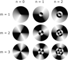
- FIG. FIG. 4 is a schematic diagram of the slow axis distribution of the phase difference pattern used in the present invention.
- 2 is a conceptual diagram of an optical communication system 2 according to Embodiment 2.
- FIG. It is a figure for demonstrating the relationship between the phase of a retardation pattern, and the direction of a liquid crystal compound.
- FIG. 2 is a conceptual diagram showing an example of a phase difference pattern used in the present invention in terms of phase distribution; It is the figure which represented each phase difference pattern with phase distribution, and the figure which represented each phase difference pattern with slow-axis distribution. It is the figure which represented each phase difference pattern with phase distribution, and the figure which represented each phase difference pattern with slow-axis distribution.
- FIG. 4 is a conceptual diagram showing another example of the phase difference pattern used in the present invention in terms of phase distribution
- FIG. 2 is a conceptual diagram of an exposure mask used when producing a retardation pattern used in the present invention, and a diagram showing the polarization direction of light for exposure.
- FIG. 2 is a conceptual diagram of an exposure mask used when producing a retardation pattern used in the present invention, and a diagram showing the polarization direction of light for exposure.
- FIG. 2 is a conceptual diagram of an exposure mask used when producing a retardation pattern used in the present invention, and a diagram showing the polarization direction of light for exposure.
- FIG. 2 is a conceptual diagram of an exposure mask used when producing each phase difference pattern
- FIG. 2 is a conceptual diagram of an exposure mask used when producing each phase difference pattern
- FIG. 2 is a conceptual diagram of an exposure mask used when producing each phase difference pattern;
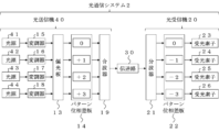
- FIG. 1 is a conceptual diagram showing the configuration of an optical communication system 1 according to Embodiment 1 of the present invention.
- An optical communication system 1 connects an optical transmitter 10 that transmits a plurality of signal lights, an optical receiver 20 that receives a plurality of signal lights transmitted from the optical transmitter 10, and the optical transmitter 10 and the optical receiver 20. It has a transmission line 30 that
- the optical transmitter 10 has a light source 11 , a beam spreading element 12 , a polarizing plate 13 , a patterned retardation plate 14 , modulators 15 to 18 and a multiplexer 19 .
- the light source 11 must be a polarized light source, but the light source itself may emit polarized light, or the light source may have a polarizing plate.
- the light emitted from the light source 11 is preferably near-infrared light. Near-infrared light is light in the wavelength range of 700 nm to 2500 nm.
- a light emitting diode (LED), a laser light source, or the like can be used as the light source 11 .
- the light emitted from the light source 11 enters the beam expanding element 12 and is expanded in the horizontal direction.
- a cylindrical lens, a microlens (combination of a convex lens and a concave lens), or the like can be used as the beam expanding element 12 .
- the widened light enters the polarizing plate 13 and is converted into linearly polarized light.
- the polarizing plate 13 is not particularly limited as long as it has a degree of polarization corresponding to the wavelength of the light source 11, and either an absorption type or a reflection type can be used.
- each light is divided into optical vortices with different spiral directions and pitches of the spiral structure and superimposed.
- the linearly polarized light enters the pattern retardation plate 14 and is converted into optical vortices corresponding to each order.
- the pattern retardation plate 14 has a plurality of retardation patterns for converting incident linearly polarized light into optical vortices.
- the number of retardation patterns that the patterned retardation plate has may be 2 to 3, or may be 5 or more. That is, the number of m can be adjusted as needed.
- Each phase difference pattern preferably has a configuration in which the azimuth angle of the slow axis in the plane changes discretely or continuously in the circumferential direction around one point, and in particular, the azimuth angle of the slow axis is More preferably, it changes discretely or continuously by ⁇ 180° ( ⁇ is an integer) when making one turn around one point.
- ⁇ is an integer
- m +1
- the direction of the slow axis changes counterclockwise (counterclockwise) by 180° when one rotation is made counterclockwise about the central point. becomes.
- the phase difference between the patterned retardation plate 14 and the patterned retardation plate 22 is preferably ⁇ /2 with respect to the wavelength ⁇ of the incident light.
- the retardation patterns of the patterned retardation plates 14 and 22 can be produced by a known method. As a specific example, it can be produced by the method described in JP-A-2008-233903.
- the polarizing plate 13 and the pattern retardation plate 14 may be integrated.
- a known bonding method such as an adhesive and/or an adhesive may be used.
- the integration has the advantage of reducing the loss of light due to reflection on the air interface and simplifying the assembly because the number of parts is reduced.
- the pattern retardation plate 14 and the pattern retardation plate 22, which will be described later, preferably have an alignment mechanism capable of accurately aligning the incident position of the incident light with the center of each retardation pattern. By precisely aligning the incident position of the incident light with the center of each phase difference pattern, the conversion efficiency can be maximized and the S/N ratio of communication is improved.
- a plurality of optical vortices generated by passing through each phase difference pattern are incident on modulators 15 to 18, respectively.
- the modulators 15 to 18 modulate the amplitude of the incident optical vortex.
- the amplitude of each optical vortex is modulated by the modulators 15 to 18 only for the optical vortex of the order corresponding to the required signal.
- Amplitude modulation may be two-step digital modulation or multi-step modulation.
- the modulators 15 to 18 for example, MEMS (Micro-Electro-Mechanical Systems) mirrors and LCOS (Liquid Crystal On Silicon) elements can be used.
- a different signal is assigned to each optical vortex by the modulators 15-18.
- the optical vortices modulated by the modulators 15 to 18 are multiplexed by the multiplexer 19 and transmitted to the transmission line 30 .
- the multiplexer 19 is not limited, and various known multiplexers can be used.
- Transmission line 30 may be free space, but is preferably optical fiber for S/N ratio and stability.
- the optical fiber is not particularly limited, and any optical fiber generally used in optical communication systems can be used.
- optical receiver 20 constituting the optical communication system of the present invention
- a known receiver for optical vortex can be applied. That is, it is sufficient that the signal can be reproduced from the amplitude of each channel after demultiplexing the optical vortex with an appropriate demultiplexer.
- FIG. 1 The configuration shown in FIG. 1 is a preferred example of the optical receiver 20.
- FIG. The optical receiver 20 has a demultiplexer 21, a pattern phase difference plate 22, and light receiving elements 23-26.
- the transmitted optical signal (multiplexed optical vortex) is demultiplexed by the demultiplexer 21 so that it can be incident on each phase difference pattern of the pattern phase difference plate 22 .
- the pattern retardation plate 22 has the same order as the phase difference pattern of the pattern retardation plate 14, but has the same absolute value but a different sign.
- an optical signal is incident on a phase difference pattern with the same absolute value as the order of the optical vortex that has passed through the modulators 15 to 18 but with a different sign, the 0th-order light with the maximum optical intensity at the central portion is generated.
- zero-order light is not generated, and the donut-shaped light intensity distribution of the light vortex is maintained, so the light intensity becomes 0 at the central portion. That is, each phase difference pattern of the patterned phase difference plate 22 intensifies only the light intensity of the central portion of the light vortex of the corresponding order.
- each phase difference pattern of the pattern phase difference plate 22 is received by the light receiving elements 23 to 26, and if the light intensity of the central portion is measured, an optical signal corresponding to the order of the optical vortex passed by the optical transmitter 10 is obtained. is detected. Thereby, the signal assigned to each optical vortex can be detected.
- the optical system is simple and highly efficient multiplex optical communication is possible by using the optical vortex generated by the phase difference pattern.
- FIG. 3 is a conceptual diagram showing the configuration of an optical communication system 2 according to Embodiment 2 of the present invention.
- the optical transmitter 40 has light sources 41 to 44 consisting of a plurality of light sources, that there is no beam spreading element 12, and that the modulators 15 to 18 are the light sources 41 to 44 and the polarizing plate 13. It differs from the first embodiment in that it is arranged between them. Except for this point, the second embodiment is the same as the first embodiment.
- the optical transmitter 40 has light sources 41 - 44 , modulators 15 - 18 , a polarizing plate 13 , a pattern retardation plate 14 and a multiplexer 16 .
- the light sources 41 to 44 are arranged in the same number as the number of the phase difference patterns arranged on the pattern retardation plate 14. By turning ON/OFF the light sources 41 to 44 or applying modulation by the modulators 15 to 18, Signal can be switched.
- the light sources 41 to 44 are not particularly limited, and light sources generally used in optical communication systems can be used, but near-infrared light is preferred.
- the lights emitted from the light sources 41 to 44 enter the polarizing plate 13 and are converted into linearly polarized light, enter the phase difference patterns of each order on the pattern phase difference plate 14 , and generate optical vortices of each order. integrated with.
- the subsequent transmission line 30 and optical receiver 20 are the same as in the first embodiment.
- the optical system is simple and highly efficient multiplex optical communication is possible by using the optical vortex generated by the phase difference pattern.
- the optical communication system 2 is configured to have the modulators 15 to 18 between the light sources 41 to 44 and the polarizing plate 13, but is not limited to this. and the multiplexer 19, the modulators 15 to 18 may be provided.
- the patterned retardation plate has a configuration in which a plurality of retardation patterns are arranged in one direction, but the pattern is not limited to this, and may be arranged two-dimensionally.
- the beam expanding element may expand the light in two orthogonal directions, or a plurality of light sources may be arranged in two directions according to the arrangement of the phase difference patterns. May be ordered in dimension order.
- a plurality of light sources may be arranged in one direction, and the light emitted from each light source may be widened by a plurality of beam widening elements in a direction perpendicular to the arrangement direction of the light sources.
- the retardation pattern of the patterned retardation plate of the optical communication system of the present invention will be described in more detail below.
- the patterned retardation plate is preferably a liquid crystal layer formed using a composition containing a liquid crystal compound, and each retardation pattern is such that the optic axis derived from the liquid crystal compound is oriented in a pattern described later. is preferred.
- FIG. 4 is a diagram showing the relationship between the orientation of the optical axis and the normalized phase for each minute area.
- FIG. 4 shows the direction of the optical axis (slow axis) of each minute region in the phase difference pattern as a normalized phase from 0 to 2 ⁇ , visualized in a gray scale with 0 being black and 2 ⁇ being white. is.
- Reference numeral 50 in FIG. 4 represents (orientation of the optical axis of) the liquid crystal compound.
- phase 1 the state in which the optical axis 50 faces the horizontal direction in the figure (the angle of the optical axis in the polar coordinate display is 0°) is defined as phase 0.
- a state in which the optical axis 50 is rotated counterclockwise by 180° is defined as a phase 2 ⁇ , and the phase is normalized according to the counterclockwise rotation angle.
- the phase is ⁇ /2 when the optical axis 50 is rotated counterclockwise by 45° (the second optical axis 50 from the left), and the phase is ⁇ /2 when the optical axis 50 is rotated by 90° (the third optical axis 50 from the left).
- the 135° rotated state (second optical axis 50 from the right) has a phase of 3 ⁇ /2.
- the change in the optical axis 50 is actually a continuous change, and the optical axis (liquid crystal compound) 50 oriented at an angle therebetween exists between the optical axes 50 in FIG.
- the states of the optical axes of phase 0 and phase 2 ⁇ are the same.
- the phase of the phase difference pattern is represented in grayscale, and the orientation of the optical axis 50 is superimposed.
- the direction of the optic axis 50 in minute regions in the liquid crystal layer is the direction of the optic axis derived from the liquid crystal compound. Therefore, the optical axis 50 in FIG. 5 can also be said to be the optical axis of the liquid crystal compound.
- the liquid crystal compound is a rod-like liquid crystal compound
- the long axis of the rod-like liquid crystal compound is the optical axis derived from the liquid crystal compound.
- the axis perpendicular to the discotic surface of the discotic liquid crystal compound is the optical axis.
- the direction of the optic axis (liquid crystal compound) 50 in the minute area rotates counterclockwise when viewed counterclockwise in the circumferential direction.
- the optical axis 50 rotates by half (180°) during one turn in the circumferential direction from the position where the phase is 0, that is, the phase gradually changes from 0 to 2 ⁇ .
- the direction of the optical axis (liquid crystal compound) 50 in the minute area is counterclockwise.
- the optical axis 50 rotates once in the circumferential direction from the position where the phase is 0, and the optical axis 50 rotates once (360°), that is, the phase repeats the phase change from 0 to 2 ⁇ twice.
- the direction of the optical axis (liquid crystal compound) 50 in the minute area is counterclockwise. While rotating, the optical axis 50 rotates once and a half (540°) during one turn in the circumferential direction from the position where the phase is 0, that is, the phase repeats the phase change from 0 to 2 ⁇ three times. .
- examples of retardation patterns possessed by patterned retardation layers are represented by phases (gray scale) normalized from 0 to 2 ⁇ .
- the phase difference pattern has a phase that changes in the circumferential direction and a constant phase in the radial direction, but is not limited to this.
- the retardation pattern of the patterned retardation layer may have nodes with discontinuous phases in the radial direction.
- FIG. 6 shows another example of the retardation pattern possessed by the patterned retardation layer.
- the diagram on the left side is a diagram showing the phase difference pattern
- the diagram on the right side is a schematic diagram of the slow axis distribution of the phase difference pattern.
- the phase when viewed counterclockwise in the circumferential direction, gradually changes from 0 to 2 ⁇ during one turn in the circumferential direction from the position where the phase is 0.
- the position of the phase 0 in the circumferential direction is shifted by 90° between the circular area and the annular area.
- the position of the phase 0 in the circumferential direction is shifted by 60° between the circular area and the annular area.
- the patterned retardation plate of the optical communication system of the present invention may include a retardation pattern having nodes.
- the phase gradually changes from 0 to 2 ⁇ during one turn in the circumferential direction from the position where the phase is 0. .
- the position of the phase 0 in the circumferential direction is shifted by 180° between the circular area and the first annular area.
- the position of the phase 0 in the circumferential direction is shifted by 180° between the first annular region and the second annular region. In other words, the non-adjacent circular region and the second annular region coincide in the position where the phase is 0 in the circumferential direction.
- the position of the phase 0 in the circumferential direction is shifted by 90° between the circular region and the first annular region.
- the position of the phase 0 in the circumferential direction is shifted by 90° between the first annular region and the second annular region. In other words, the non-adjacent circular region and the second annular region coincide in the position where the phase is 0 in the circumferential direction.
- the position of the phase 0 in the circumferential direction is shifted by 60° between the circular area and the first annular area.
- the position of the phase 0 in the circumferential direction is shifted by 60° between the first annular region and the second annular region. In other words, the non-adjacent circular region and the second annular region coincide in the position where the phase is 0 in the circumferential direction.
- the patterned retardation plate of the optical communication system of the present invention may include retardation patterns having different numbers of nodes and/or different orders.
- the patterned retardation plate of the present invention is a patterned retardation plate having a plurality of retardation patterns for converting incident polarized light into an optical vortex, and having a plurality of retardation patterns of different orders in the same plane. .
- the retardation patterns possessed by the patterned retardation plate are as described above, and the patterned retardation plate has retardation patterns with different numbers of nodes and/or different orders in the same plane.
- the method of forming the retardation pattern is not particularly limited.
- the patterned retardation plate is a liquid crystal layer formed by aligning a liquid crystal compound in a predetermined alignment state
- a liquid crystal composition containing a liquid crystal compound is used as an alignment film for aligning the liquid crystal compound in a predetermined retardation pattern.
- a liquid crystal phase in which the direction of the optic axis derived from the liquid crystal compound is oriented in a retardation pattern is formed by coating on the liquid crystal compound, and the liquid crystal phase is fixed in a layer.
- the liquid crystal layer may be formed by multi-layer coating.
- Multi-layer coating means that the first layer of the liquid crystal composition is first applied on the alignment film, heated, cooled, and then UV-cured to prepare a liquid crystal fixing layer, and the second and subsequent layers are applied to the liquid crystal fixing layer.
- a liquid crystal layer is formed by repeatedly applying multiple coats, heating, cooling, and curing with ultraviolet rays until a desired thickness is obtained.
- the alignment film is an alignment film for aligning the liquid crystal compound in a predetermined retardation pattern when forming the liquid crystal layer.
- a so-called photo-alignment film obtained by irradiating a photo-alignment material with polarized or non-polarized light to form an alignment film is preferably used. That is, in the present invention, a photo-alignment film formed by coating a support with a photo-alignment material, for example, is preferably used as the alignment film. Irradiation with polarized light can be performed in a direction perpendicular to or oblique to the photo-alignment film, and irradiation with non-polarized light can be performed in a direction oblique to the photo-alignment film.
- photo-alignment materials used in the alignment film include, for example, JP-A-2006-285197, JP-A-2007-76839, JP-A-2007-138138, and JP-A-2007-94071.
- Preferable examples include photodimerizable compounds described in JP-A-177561 and JP-A-2014-12823, particularly cinnamate compounds, chalcone compounds and coumarin compounds.
- azo compounds, photocrosslinkable polyimides, photocrosslinkable polyamides, photocrosslinkable polyesters, cinnamate compounds, and chalcone compounds are preferably used.
- the thickness of the alignment film is not limited, and the thickness may be appropriately set according to the material for forming the alignment film so that the required alignment function can be obtained.
- the thickness of the alignment film is preferably 0.01 to 5 ⁇ m, more preferably 0.05 to 2 ⁇ m.
- the preferred method of exposing the alignment film for forming the alignment pattern includes a method of exposing the alignment film by a direct writing method, and a method of subjecting the alignment film to multiple times of polarized light exposure using masks having different exposure patterns. , are mentioned.
- a support having an alignment film is placed on an XY stage, a linearly polarized light beam is passed through a ⁇ /2 plate and focused on the alignment film, and the XY stage is moved to achieve alignment.
- the polarization direction of the linearly polarized light is converted to an arbitrary direction, thereby drawing a desired alignment pattern on the alignment film.
- the rotation of the ⁇ /2 plate and the movement of the XY stage are controlled by, for example, a computer, so that the position on the surface of the alignment film where the light is focused and the direction of polarization of the light correspond to each other.
- a desired orientation pattern can be formed thereon.
- the intensity of the light to be irradiated, the exposure time, and the like may be appropriately set according to the material for forming the alignment film and the like.
- the amount of exposure per unit area can be adjusted by the intensity of the irradiated light and the scanning speed. It is preferably 100 mJ/m 2 or more, more preferably 150 mJ/m 2 , from the viewpoint of performing sufficient exposure to give alignment to the alignment film. Also, from the viewpoint of preventing deterioration of orientation due to excessive irradiation, it is preferably 5 J/m 2 or less, more preferably 3 J/m 2 or less.
- the spot diameter of the light beam focused on the alignment film may be any size that can impart a desired alignment pattern to the alignment film.
- a method of performing polarization exposure multiple times using masks having different exposure patterns (hereinafter also referred to as multiple polarization exposure method) will be described below.
- the multiple polarized exposure method includes, for example, a step of subjecting the photo-alignment film to polarized light exposure three times.
- the exposure methods are different from each other.
- An example of the multiple polarization exposure method will be described with reference to FIGS. 9 to 11. FIG.
- the upper diagram in FIG. 9 is a diagram conceptually showing the mask used for the first polarized exposure, and the lower diagram in FIG. 9 shows the polarization direction of the linearly polarized light irradiated in the first polarized exposure. is an arrow.
- the upper diagram in FIG. 10 conceptually shows the mask used for the second polarized exposure, and the lower diagram in FIG. 10 shows the polarization direction of the linearly polarized light irradiated in the second polarized exposure. is an arrow indicating
- the upper diagram in FIG. 11 conceptually illustrates the mask used for the third polarized exposure, and the lower diagram in FIG. 11 illustrates the polarization direction of the linearly polarized light irradiated in the third polarized exposure.
- the transmittance of the mask used in each polarization exposure is represented by white areas with high transmittance (eg, 100%) and black areas with low transmittance (eg, 0%). It is a figure represented by gray scale.
- the transmittance is lowest at positions 180° in the circumferential direction from the highest transmittance position, and the transmittance It has a transmittance pattern with a graded transmittance.
- the positions of the masks used for the first to third polarized exposures where the transmittance is highest are shifted in the circumferential direction. Specifically, the position where the transmittance of the mask for the second time is the highest is shifted by 120° in the circumferential direction from the position where the transmittance of the mask for the first time is the highest.
- the position where the transmittance of the third mask is highest is displaced from the position where the transmittance of the first mask is highest by 240° (120° relative to the second mask) in the circumferential direction.
- the polarization direction of the linearly polarized light used for the first polarized exposure is orthogonal to the direction in which the transmittance of the first mask is highest (rightward direction in the figure).
- the polarization direction of the linearly polarized light used for the second polarized light exposure is shifted counterclockwise by 60° from the polarization direction of the first linearly polarized light.
- the polarization direction of the linearly polarized light used for the third polarized light exposure is shifted clockwise by 60° ( ⁇ 60°) from the polarization direction of the first linearly polarized light. That is, the polarization direction of the linearly polarized light used for the third polarized light exposure is shifted clockwise by 120° ( ⁇ 120°) from the polarization direction of the second linearly polarized light.
- an alignment regulating force is generated in a direction orthogonal to the polarization direction of the irradiated linearly polarized light. Therefore, at the position in the direction of azimuth 0° (right side in the figure), the transmittance of the first mask is high, and the transmittance of the second and third masks is lower than the transmittance of the first mask and substantially the same. Therefore, when the polarization directions of the first to third times are superimposed, the film is exposed to linearly polarized light in the vertical direction in the drawing, and an orientation regulating force is generated in the direction (horizontal direction) perpendicular to this.
- the transmittance of the first mask is low, and the transmittance of the second and third masks is higher than that of the first time and substantially the same.
- the film is exposed to linearly polarized light in the left-right direction in the figure, and an alignment regulating force is generated in the up-down direction in the figure.
- the orientation for forming a retardation pattern in which the direction of the orientation regulating force changes for each position in the plane of the orientation film and the azimuth angle of the slow axis changes when making one turn around a certain point. Patterns can be formed.
- the order of polarized light exposure is not limited to the above, and a desired alignment pattern can be obtained even in a different order from the above by performing polarized light exposure three times using a mask and different polarized lights.
- the polarization direction of polarized light exposure and the alignment direction of the liquid crystal may be the same. In that case, a desired alignment pattern can be obtained by appropriately rotating each exposure mask pattern by the same angle accordingly.
- the polarized light exposure is performed three times, but there is no limitation to this, and the polarized light exposure may be performed four times or more as long as a desired orientation pattern can be obtained.
- the transmittance distribution of the mask used in each polarized light exposure and the polarization direction of the linearly polarized light to be irradiated are not limited to the above examples as long as the desired alignment pattern can be obtained.
- the transmittance distribution of the mask used in each polarized light exposure and the polarization direction of the linearly polarized light to be irradiated may be appropriately set according to the desired alignment pattern.
- each phase difference pattern shown in FIGS. 5 to 7 can be formed.
- masks with different transmittance patterns are arranged in the in-plane direction and polarized light exposure can be performed using the same linearly polarized light.
- By forming a liquid crystal layer on such an alignment film having a plurality of alignment patterns it is possible to manufacture a patterned retardation plate having retardation patterns of different orders in the same plane.
- liquid crystal layer A liquid crystal layer is formed on the surface of the alignment film.
- the liquid crystal layer is a liquid crystal layer formed by fixing a liquid crystal phase in which a liquid crystal compound is aligned, and is a liquid crystal layer having a retardation pattern.
- the liquid crystal layer can be formed by fixing a liquid crystal phase in which a liquid crystal compound is oriented in a retardation pattern.
- the structure in which the liquid crystal phase is fixed may be a structure in which the alignment of the liquid crystal compound that is the liquid crystal phase is maintained, and typically, the polymerizable liquid crystal compound is aligned along the retardation pattern.
- the structure is polymerized and cured by UV irradiation, heating, or the like to form a layer having no fluidity, and at the same time, the structure is changed to a state in which the orientation is not changed by an external field or external force.
- the liquid crystal compound does not have to exhibit liquid crystallinity in the liquid crystal layer.
- the polymerizable liquid crystal compound may be polymerized by a curing reaction and lose liquid crystallinity.
- a liquid crystal composition containing a liquid crystal compound is an example of a material used for forming a liquid crystal layer having a fixed liquid crystal phase.
- the liquid crystal compound is preferably a polymerizable liquid crystal compound.
- the liquid crystal composition used for forming the liquid crystal layer may further contain a surfactant, a polymerization initiator, and the like.
- the polymerizable liquid crystal compound may be a rod-like liquid crystal compound or a discotic liquid crystal compound.
- An example of the rod-like polymerizable liquid crystal compound forming the liquid crystal layer is a rod-like nematic liquid crystal compound.
- Rod-shaped nematic liquid crystal compounds include azomethines, azoxys, cyanobiphenyls, cyanophenyl esters, benzoic acid esters, cyclohexanecarboxylic acid phenyl esters, cyanophenylcyclohexanes, cyano-substituted phenylpyrimidines, and alkoxy-substituted phenylpyrimidines.
- phenyldioxane, tolan, and alkenylcyclohexylbenzonitriles are preferably used. Not only low-molecular-weight liquid crystal compounds but also high-molecular liquid-crystal compounds can be used.
- the alignment of the rod-shaped liquid crystal compound it is more preferable to fix the alignment of the rod-shaped liquid crystal compound by polymerization.
- the polymerizable rod-shaped liquid crystal compound Makromol. Chem. , vol. 190, pp. 2255 (1989), Advanced Materials vol. 5, pp. 107 (1993), US Pat. 95/24455, 97/00600, 98/23580, 98/52905, JP-A-1-272551, JP-A-6-16616, JP-A-7-110469, JP-A-11-80081 No. 2001-64627, etc.
- the rod-like liquid crystal compound for example, those described in JP-A-11-513019 and JP-A-2007-279688 can also be preferably used.
- two or more types of polymerizable liquid crystal compounds may be used in combination. When two or more kinds of polymerizable liquid crystal compounds are used together, the alignment temperature can be lowered.
- polymerizable groups examples include unsaturated polymerizable groups, epoxy groups, and aziridinyl groups, preferably unsaturated polymerizable groups, and more preferably ethylenically unsaturated polymerizable groups.
- Polymerizable groups can be introduced into molecules of liquid crystal compounds by various methods.
- the number of polymerizable groups possessed by the polymerizable liquid crystal compound is preferably 1 to 6, more preferably 1 to 3.
- a cyclic organopolysiloxane compound having a cholesteric phase as disclosed in JP-A-57-165480 can be used as polymerizable liquid crystal compounds other than the above.
- the polymer liquid crystal compounds described above there are polymers in which mesogenic groups exhibiting liquid crystal are introduced into the main chain, side chains, or both of the main chain and side chains, and polymer cholesteric compounds in which cholesteryl groups are introduced into the side chains.
- Liquid crystals, liquid crystalline polymers as disclosed in JP-A-9-133810, and liquid-crystalline polymers as disclosed in JP-A-11-293252 and the like can be used.
- Discotic Liquid Crystal Compound As the discotic liquid crystal compound, for example, those described in JP-A-2007-108732 and JP-A-2010-244038 can be preferably used.
- the liquid crystal compound rises in the thickness direction in the liquid crystal layer, and the optical axis derived from the liquid crystal compound is an axis perpendicular to the disc surface, a so-called fast phase. Defined as an axis.
- the amount of the polymerizable liquid crystal compound added in the liquid crystal composition is preferably 75 to 99.9% by mass, and preferably 80 to 99%, based on the solid content mass (mass excluding the solvent) of the liquid crystal composition. % by mass is more preferred, and 85 to 90% by mass is even more preferred.
- liquid crystal compound a liquid crystal compound having a high refractive index anisotropy ⁇ n can be preferably used in order to obtain high diffraction efficiency.
- the liquid crystal composition used for forming the liquid crystal layer may contain a surfactant.
- the surfactant is preferably a compound that can stably or quickly function as an alignment control agent that contributes to the alignment of the liquid crystal compound.
- Examples of surfactants include silicone-based surfactants and fluorine-based surfactants, with fluorine-based surfactants being preferred examples.
- the surfactant include compounds described in paragraphs [0082] to [0090] of JP-A-2014-119605, and compounds described in paragraphs [0031] to [0034] of JP-A-2012-203237. , compounds exemplified in paragraphs [0092] and [0093] of JP-A-2005-99248, paragraphs [0076] to [0078] and paragraphs [0082] to [0085] of JP-A-2002-129162 compounds exemplified therein, and fluorine (meth)acrylate polymers described in paragraphs [0018] to [0043] of JP-A-2007-272185.
- surfactant may be used individually by 1 type, and may use 2 or more types together.
- fluorosurfactant compounds described in paragraphs [0082] to [0090] of JP-A-2014-119605 are preferable.
- the amount of the surfactant added in the liquid crystal composition is preferably 0.01 to 10% by mass, more preferably 0.01 to 5% by mass, and 0.02 to 2% by mass with respect to the total mass of the liquid crystal compound. is more preferred.
- the liquid crystal composition contains a polymerizable compound, it preferably contains a polymerization initiator.
- the polymerization initiator used is preferably a photopolymerization initiator capable of initiating the polymerization reaction by ultraviolet irradiation.
- photoinitiators include ⁇ -carbonyl compounds (described in US Pat. Nos. 2,367,661 and 2,367,670), acyloin ethers (described in US Pat. No. 2,448,828), ⁇ -hydrocarbons substituted aromatic acyloin compounds (described in US Pat. No.
- the content of the photopolymerization initiator in the liquid crystal composition is preferably 0.1 to 20% by mass, more preferably 0.5 to 12% by mass, based on the content of the liquid crystal compound.
- the liquid crystal composition may optionally contain a cross-linking agent in order to improve film strength and durability after curing.
- a cross-linking agent those that are cured by ultraviolet rays, heat, moisture, etc. can be preferably used.
- the cross-linking agent is not particularly limited and can be appropriately selected depending on the intended purpose.
- polyfunctional acrylate compounds such as trimethylolpropane tri(meth)acrylate and pentaerythritol tri(meth)acrylate
- epoxy compounds such as ethylene glycol diglycidyl ether
- aziridine compounds such as 2,2-bishydroxymethylbutanol-tris[3-(1-aziridinyl)propionate] and 4,4-bis(ethyleneiminocarbonylamino)diphenylmethane
- hexa isocyanate compounds such as methylene diisocyanate and biuret-type isocyanate
- alkoxysilane compounds such as vinyltrimethoxysilane and N-(2-aminoethyl)3-aminopropyltrimethoxysilane, etc.
- the content of the cross-linking agent is preferably 3 to 20% by mass, more preferably 5 to 15% by mass, based on the solid mass of the liquid crystal composition. When the content of the cross-linking agent is within the above range, the effect of improving the cross-linking density is likely to be obtained, and the stability of the liquid crystal phase is further improved.
- the liquid crystal composition may further contain polymerization inhibitors, antioxidants, ultraviolet absorbers, light stabilizers, colorants, metal oxide fine particles, etc., within a range that does not reduce optical performance. can be added at
- the liquid crystal composition is preferably used as a liquid when forming the liquid crystal layer.
- the liquid crystal composition may contain a solvent.
- the solvent is not limited and can be appropriately selected according to the purpose, but organic solvents are preferred.
- the organic solvent is not limited and can be appropriately selected depending on the purpose. Examples include ketones, alkyl halides, amides, sulfoxides, heterocyclic compounds, hydrocarbons, esters, and ethers. etc. These may be used individually by 1 type, and may use 2 or more types together. Among these, ketones are preferred in consideration of the load on the environment.
- a liquid crystal composition is applied to the surface on which the liquid crystal layer is to be formed, and the liquid crystal compound is aligned in a predetermined liquid crystal alignment pattern to form a liquid crystal phase, and then the liquid crystal compound is cured.
- a liquid crystal layer preferably a liquid crystal layer. That is, when the liquid crystal layer is formed on the alignment film, the liquid crystal composition is applied to the alignment film, the liquid crystal compound is aligned in a predetermined liquid crystal alignment pattern, and then the liquid crystal compound is cured to fix the liquid crystal phase. It is preferable to form a liquid crystal layer formed by The liquid crystal composition can be applied by printing methods such as inkjet and scroll printing, and known methods such as spin coating, bar coating and spray coating, which can uniformly apply the liquid to the sheet.
- the applied liquid crystal composition is dried and/or heated as necessary, and then cured to form a liquid crystal layer.
- the liquid crystal compound in the liquid crystal composition may be aligned in a predetermined liquid crystal alignment pattern.
- the heating temperature is preferably 200° C. or lower, more preferably 130° C. or lower.
- the aligned liquid crystal compound is further polymerized as necessary.
- Polymerization may be either thermal polymerization or photopolymerization by light irradiation, but photopolymerization is preferred.
- the irradiation energy is preferably 20 mJ/cm 2 to 50 J/cm 2 , more preferably 50 to 1500 mJ/cm 2 .
- light irradiation may be performed under heating conditions or under a nitrogen atmosphere.
- the wavelength of the ultraviolet rays to be irradiated is preferably 250 to 430 nm.
- the thickness of the liquid crystal layer is not limited, and may be appropriately set according to the application of the liquid crystal layer, the material for forming the liquid crystal layer, and the like.
- the value of in-plane retardation (Re) in minute regions is half the wavelength of the light emitted from the light source of the optical communication system (for example, near-infrared light), that is, ⁇ /2. is preferred.
- the in-plane retardation is calculated from the product of the refractive index difference ⁇ n accompanying the refractive index anisotropy in the region and the thickness of the liquid crystal layer.
- the refractive index difference associated with the refractive index anisotropy of the region in the liquid crystal layer is the difference between the refractive index in the slow axis direction and the refractive index in the direction orthogonal to the slow axis direction in the plane of the region. is the refractive index difference defined by the difference.
- the refractive index difference ⁇ n accompanying the refractive index anisotropy of the region is the difference between the refractive index of the liquid crystal compound in the direction of the optical axis and the refractive index of the liquid crystal compound in the direction perpendicular to the optical axis in the plane of the region. be equivalent to. That is, the refractive index difference ⁇ n is equal to the refractive index difference of the liquid crystal compound.
- liquid crystal layer functions as a so-called ⁇ /2 plate
- the present invention includes a mode in which a laminate integrally including a support and an alignment film functions as a ⁇ /2 plate.
- optical communication system and the patterned retardation plate of the present invention have been described in detail above, the present invention is not limited to the above examples, and various improvements and modifications can be made without departing from the gist of the present invention. Of course it is also good.
- Example 1 ⁇ Production of liquid crystal layer> (support) A flat glass substrate was prepared as a support.
- the following coating solution for forming an alignment film was applied onto the support by spin coating.
- the support on which the coating film of the alignment film-forming coating liquid was formed was dried on a hot plate at 60° C. for 60 seconds to form an alignment film.
- Photo-alignment material A 1.00 parts by mass Water 16.00 parts by mass Butoxy ethanol 42.00 parts by mass Propylene glycol monomethyl ether 42.00 parts by mass ⁇ ⁇
- composition A-1 As a liquid crystal composition for forming a liquid crystal layer, the following composition A-1 was prepared.
- Composition A-1 Liquid crystal compound L-1 100.00 parts by mass Polymerization initiator (manufactured by BASF, Irgacure OXE01) 1.00 parts by mass Leveling agent T-1 0.08 parts by mass Methyl ethyl ketone 1050.00 parts by mass ⁇ ⁇
- the liquid crystal layer was formed by coating the composition A-1 on the alignment film P-1 in multiple layers.
- Multi-layer coating means that the first layer composition A-1 is first applied on the alignment film, and after heating and UV curing to prepare a liquid crystal fixing layer, the second and subsequent layers are applied to the liquid crystal fixing layer. It refers to repeating the process of coating in layers and then curing with UV rays after heating in the same manner.
- the above composition A-1 is applied on the alignment film P-1, the coating film is heated to 80 ° C. on a hot plate, and then a high-pressure mercury lamp is used in a nitrogen atmosphere.
- the alignment of the liquid crystal compound was fixed by irradiating the coating film with ultraviolet rays of 365 nm at an irradiation amount of 300 mJ/cm 2 .
- the second and subsequent layers were overcoated on this liquid crystal fixing layer, heated under the same conditions as above, and then UV-cured to prepare a liquid crystal fixing layer.
- the liquid crystal layer was formed by repeating coating until the total thickness reached a desired thickness.
- the thickness of the liquid crystal layer was set to 2.0 ⁇ m.
Landscapes
- Physics & Mathematics (AREA)
- Engineering & Computer Science (AREA)
- Computer Networks & Wireless Communication (AREA)
- Signal Processing (AREA)
- General Physics & Mathematics (AREA)
- Optics & Photonics (AREA)
- Polarising Elements (AREA)
Abstract
本発明によれば、光学系がシンプルで高効率な多重光通信システムを提供することができる。光送信機と、伝送路と、光受信機を含み、光送信機は、偏光光源と、偏光板と、偏光光源からの光を複数の光渦に変換するパターン位相差板と、変調器と、合波器とを含む、光通信システム。
Description
本発明は、光通信システムに関する。
インターネット上の通信量は年々増大しており、基幹ネットワークである光通信システムにおいても大容量化が求められている。
光通信システムの大容量化を実現するために空間分割多重による光通信システムが検討されている。例えば、非特許文献1には、15種類の異なるモードの光を利用した光通信システムが提案されている。
Georg Rademacher, Benjamin J. Puttnam, Ruben S. Luis, Tobias A. Eriksson, Nicolas K. Fontaine, Mikael Mazur, Haoshuo Chen, Roland Ryf, David T. Neilson, Pierre Sillard, Frank Achten, Yoshinari Awaji and Hideaki Furukawa, Nature Communications, vol. 12, Article number: 4238, 2021年
しかしながら、従来技術では光のモードを変換するのに反射型の複雑な光学系が必要であり、さらに変換効率が低いという問題があった。
そこで本発明は、光学系がシンプルで高効率な多重光通信システムを提供することを課題とする。
本発明者らが鋭意検討の結果、パターン位相差板を適用し、入射する複数の光線または拡張されて入射する光が、前記パターン位相差板を1回通過するだけで、複数の異なるモードの光渦に変換する構成を採用することにより、光学系がシンプルで高効率な多重光通信システムを提供できることを見出した。
すなわち、以下の構成により上記課題を達成することができることを見出した。
[1]光送信機と、
伝送路と、
光受信機を含み、
光送信機は、偏光光源と、偏光光源からの光を複数の光渦に変換するパターン位相差板と、変調器と、合波器とを含む、光通信システム。
[2]偏光光源が複数個、ないしは1つの偏光光源から拡幅で分配する構成であり、パターン位相差板と合波器の間に変調器を含む、[1]に記載の光通信システム。
[3]偏光光源が複数個であり、それぞれの偏光光源とパターン位相差板との間に変調器がそれぞれある、[1]に記載の光通信システム。
[4]パターン位相差板は、面内の遅相軸の方位角が、ある1点を中心に変化するものを含む、[1]~[3]のいずれかに記載の光通信システム。
[5]パターン位相差板は、ある1点を中心に1周したときの遅相軸の方位角がα×180°(αは整数)だけ連続的に変化するものを含む、[1]~[4]のいずれかに記載の光通信システム。
[6]さらに、偏光板を含み、
偏光板と、パターン位相差板が一体になっている、[1]~[5]のいずれかに記載の光通信システム。
[7]パターン位相差板の中心と光の入射位置を正確に合わせることができる位置合わせ機構を備えた[1]~[6]のいずれかに記載の光通信システム。
[8]パターン位相差板は、次数および節の数の少なくとも一方が異なる複数の位相差パターンを同一面内に有する、[1]~[7]のいずれかに記載の光通信システム。
[9]入射する偏光を光渦に変換する位相差パターンを複数有し、
次数および節の数の少なくとも一方が異なる複数の位相差パターンを同一面内に有する、パターン位相差板。
本発明によれば、光学系がシンプルで高効率な多重光通信システムを提供することができる。
以下、本発明の実施形態について、図面を用いて詳細に説明する。ただし、本発明は多くの異なる形態による実施が可能であり、以下に示す実施形態の例示に限定されるものではない。
<実施形態1>
図1は、本発明の実施形態1による光通信システム1の構成を示す概念図である。光通信システム1は複数の信号光を送信する光送信機10と、光送信機10から送信された複数の信号光を受信する光受信機20と、光送信機10と光受信機20を接続する伝送路30を備えている。
図1は、本発明の実施形態1による光通信システム1の構成を示す概念図である。光通信システム1は複数の信号光を送信する光送信機10と、光送信機10から送信された複数の信号光を受信する光受信機20と、光送信機10と光受信機20を接続する伝送路30を備えている。
<光送信機>
光送信機10は光源11と光束拡幅素子12と偏光板13とパターン位相差板14と変調器15~18と合波器19を有している。光源11は偏光光源である必要があるが、光源そのものが偏光を出射するものでも、光源に偏光板を有するものでもよい。
光源11の出射光は、近赤外光であることが好ましい。近赤外光は700nm~2500nmの波長域の光である。光源11としては、発光ダイオード(LED)、レーザー光源等を用いることができる。
光送信機10は光源11と光束拡幅素子12と偏光板13とパターン位相差板14と変調器15~18と合波器19を有している。光源11は偏光光源である必要があるが、光源そのものが偏光を出射するものでも、光源に偏光板を有するものでもよい。
光源11の出射光は、近赤外光であることが好ましい。近赤外光は700nm~2500nmの波長域の光である。光源11としては、発光ダイオード(LED)、レーザー光源等を用いることができる。
光源11から出射された光は、光束拡幅素子12に入射し横方向に拡幅される。光束拡幅素子12としては例えばシリンドリカルレンズ、マイクロレンズ(凸レンズと凹レンズとの組み合わせ)等を使用することができる。
拡幅された光は偏光板13に入射し直線偏光に変換される。偏光板13は光源11の波長に対応した偏光度を持つものであれば特に限定されず、吸収型、反射型のいずれも使用することができる。
高効率な多重光通信を行うためには、それぞれの光が干渉しない状態で重ね合わせることが必要である。
本件では、この多重光通信のために、それぞれの光を、らせん構造のらせん方向と、そのピッチの異なる光渦に分けて重ね合わせることとしている。
本件では、この多重光通信のために、それぞれの光を、らせん構造のらせん方向と、そのピッチの異なる光渦に分けて重ね合わせることとしている。
直線偏光はパターン位相差板14に入射し、各次数に対応した、光渦に変換される。パターン位相差板14は、入射する直線偏光を光渦に変換する位相差パターンを複数有するものである。パターン位相差板14と後述するパターン位相差板22はm次(mは整数)の次数を持つ位相差パターンがそれぞれ横方向に並んでいる。なお、図1ではパターン位相差板14およびパターン位相差板22が有する位相差パターンの次数は、m=0、±1、±2、±3の場合を例示しているが、これに限定されない。パターン位相差板が有する位相差パターンの数は2~3であってもよく、あるいは、5以上であってもよい。すなわち、必要に応じてmの数を調整することができる。また、パターン位相差板が有する位相差パターンの次数mは、m=0~±3に限定はされず、+4以上あるいは-4以下であってもよい。また、パターン位相差板が有する位相差パターンの次数mは、連続しているものに限定はされず、離散的であってもよい。例えば、m=0、±2、±3、±5の次数の位相差パターンを有するものであってもよい。
各位相差パターンは面内の遅相軸の方位角がある1点を中心に周方向に離散的、もしくは、連続的に変化する構成であることが好ましく、特に遅相軸の方位角が、ある1点を中心に1周したときに、α×180°(αは整数)だけ離散的、もしくは、連続的に変化するものがより好ましい。この場合のある1点とは、任意の点を示すのではなく、その点を中心としてパターンが形成されているような点を示す。
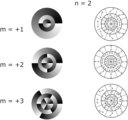
図2に、パターンの例として、m=±1~±3の位相差パターンの遅相軸分布の模式図を示す。ここで、m=+1の場合には、中央の点を中心として左回り(反時計回り)に1回転すると、遅相軸の向きが左回り(反時計回り)に180°変化していることとなる。m=+2の場合には、中央の点を中心として左回り(反時計回り)に1回転すると、遅相軸の向きが左回り(反時計回り)に360°変化していることとなる。また、m=-1の場合には、中央の点を中心として左回り(反時計回り)に1回転すると、遅相軸の向きが右回り(時計回り)に180°変化していることとなる。m=-2の場合には、中央の点を中心として左回り(反時計回り)に1回転すると、遅相軸の向きが右回り(時計回り)に360°変化していることとなる。
パターン位相差板14とパターン位相差板22の位相差は入射光の波長λに対してλ/2であることが好ましい。前述の遅相軸分布と位相差をもつ位相差パターンに直線偏光を入射させることでα=m次の次数を持つ光渦を発生させることができる。
パターン位相差板14と22の位相差パターンは公知の方法で作製することができる。具体例としては、特開2008-233903号公報に記載の方法で作製できる。
偏光板13とパターン位相差板14は一体化されていても良い。一体化する方法としては粘着剤および/または接着剤など公知の貼合方法を用いればよい。一体化することで空気界面の反射による光のロスを低減でき、部材数が減るので組立てがシンプルになるという利点がある。
パターン位相差板14と後述するパターン位相差板22には入射光の入射位置と各位相差パターンの中心を正確に合わせることができる位置合わせ機構を有していることが好ましい。入射光の入射位置と各位相差パターンの中心を正確に合わせることで、変換効率を最大化することができ、通信のS/N比が向上する。
各位相差パターンを通過して生成された複数の光渦はそれぞれ変調器15~18に入射される。
変調器15~18はそれぞれ入射する光渦に対して振幅の変調を行う。
それぞれの光渦は変調器15~18により必要な信号に対応した次数の光渦のみに振幅の変調が行われる。振幅の変調としては、二段階のデジタル変調であってもよく、多段階の変調であっても良い。変調器15~18としては、例えばMEMS(Micro―Electro-Mechanical Systems)ミラー、LCOS(Liquid Crystal On Silicon)素子を使用することができる。
変調器15~18により、各光渦には異なる信号が割り当てられる。
それぞれの光渦は変調器15~18により必要な信号に対応した次数の光渦のみに振幅の変調が行われる。振幅の変調としては、二段階のデジタル変調であってもよく、多段階の変調であっても良い。変調器15~18としては、例えばMEMS(Micro―Electro-Mechanical Systems)ミラー、LCOS(Liquid Crystal On Silicon)素子を使用することができる。
変調器15~18により、各光渦には異なる信号が割り当てられる。
各変調器15~18で変調された光渦は、合波器19で合波されて伝送路30に送信される。
合波器19としては制限はなく、種々の公知の合波器が利用可能である。
合波器19としては制限はなく、種々の公知の合波器が利用可能である。
<伝送路>
各変調器15~18を通過した光渦を合波器19により合波し、伝送路30を通して光受信機20に送信する。伝送路30は自由空間であってもよいが、S/N比および安定性の点では光ファイバーであることが好ましい。光ファイバーは特に限定されず、一般的に光通信システムに使用される光ファイバーであれば使用することができる。
各変調器15~18を通過した光渦を合波器19により合波し、伝送路30を通して光受信機20に送信する。伝送路30は自由空間であってもよいが、S/N比および安定性の点では光ファイバーであることが好ましい。光ファイバーは特に限定されず、一般的に光通信システムに使用される光ファイバーであれば使用することができる。
<光受信機>
本発明の光通信システムを構成する光受信機20としては、光渦用の受信装置であれば公知のものを適用できる。すなわち、光渦を適切な分波器で分波した後、各チャンネルの振幅から信号を再生できるものであればよい。
本発明の光通信システムを構成する光受信機20としては、光渦用の受信装置であれば公知のものを適用できる。すなわち、光渦を適切な分波器で分波した後、各チャンネルの振幅から信号を再生できるものであればよい。
図1に示す構成は、光受信機20の好ましい一例である。光受信機20は分波器21とパターン位相差板22と受光素子23~26を有している。送信された光信号(合波された光渦)は分波器21によりパターン位相差板22の各位相差パターンにそれぞれ入射できるように分波される。
パターン位相差板22はパターン位相差板14の位相差パターンの次数と絶対値は同じだが符号が異なるものが配置されている。変調器15~18を通過した光渦の次数と絶対値が同じで符号が異なる位相差パターンに光信号が入射すると、中央部分の光強度が最大になる0次光が発生する。一方で絶対値が異なる光渦が入射すると0次光は発生せず、光渦のドーナツ状の光強度分布が維持されるので中央部分は光強度が0になる。すなわち、パターン位相差板22が有する各位相差パターンは、対応する次数の光渦の中央部分の光強度のみを強める。パターン位相差板22の各位相差パターンを通過した光を、受光素子23~26で受光し、中央部分の光強度を測定すれば光送信機10で通過させた光渦の次数に対応した光信号だけが検出される。これにより、各光渦に割り当てられた信号を検出することができる。
以上に説明したように、実施形態1に係る光通信システム1によれば、位相差パターンにより発生する光渦を利用することで光学系がシンプルで高効率な多重光通信が可能となる。
<実施形態2>
図3は、本発明の実施形態2による光通信システム2の構成を示す概念図である。図3において、図1に示される構成要素と同一又は対応する構成要素には、図1に示される符号と同じ符号が付される。実施形態2は光送信機40において複数の光源からなる光源41~44を有している点と、光束拡幅素子12が無い点と、変調器15~18が光源41~44と偏光板13の間に配置される点が実施形態1と異なる。この点を除いて、実施形態2は、実施形態1と同じである。
図3は、本発明の実施形態2による光通信システム2の構成を示す概念図である。図3において、図1に示される構成要素と同一又は対応する構成要素には、図1に示される符号と同じ符号が付される。実施形態2は光送信機40において複数の光源からなる光源41~44を有している点と、光束拡幅素子12が無い点と、変調器15~18が光源41~44と偏光板13の間に配置される点が実施形態1と異なる。この点を除いて、実施形態2は、実施形態1と同じである。
<光送信機>
光送信機40は光源41~44と変調器15~18と偏光板13とパターン位相差板14と合波器16を有している。光源41~44はパターン位相差板14に配置された位相差パターンの数と同じ数だけ配置されており、光源41~44のON/OFF、または、変調器15~18による変調を加えることにより信号を切り替えることができる。光源41~44は特に限定されず、一般的に光通信システムに使用される光源であれば使用することができるが、近赤外光であることが好ましい。
光送信機40は光源41~44と変調器15~18と偏光板13とパターン位相差板14と合波器16を有している。光源41~44はパターン位相差板14に配置された位相差パターンの数と同じ数だけ配置されており、光源41~44のON/OFF、または、変調器15~18による変調を加えることにより信号を切り替えることができる。光源41~44は特に限定されず、一般的に光通信システムに使用される光源であれば使用することができるが、近赤外光であることが好ましい。
<伝送路と光受信機>
光源41~44から出射された光は偏光板13に入射し直線偏光に変換され、パターン位相差板14の各次数の位相差パターンに入射し各次数の光渦が生成され、合波器19で統合される。以降の伝送路30と光受信機20は実施形態1と同じである。
光源41~44から出射された光は偏光板13に入射し直線偏光に変換され、パターン位相差板14の各次数の位相差パターンに入射し各次数の光渦が生成され、合波器19で統合される。以降の伝送路30と光受信機20は実施形態1と同じである。
以上に説明したように、実施形態2に係る光通信システム2によれば、位相差パターンにより発生する光渦を利用することで光学系がシンプルで高効率な多重光通信が可能となる。
なお、図3に示す例では、光通信システム2において、光源41~44と偏光板13との間に変調器15~18を有する構成としたがこれに限定はされず、パターン位相差板14と合波器19との間に変調器15~18を有する構成としてもよい。
また、上述した例では、パターン位相差板は、複数の位相差パターンをある一方向に配列して有する構成としたが、これに限定はされず、2次元的に配列されていてもよい。位相差パターンが2次元的に配列されている場合には、光束拡幅素子が直交する2方向に光を拡幅するものであってもよいし、複数の光源を位相差パターンの配列に合わせて2次元定期に配列してもよい。あるいは、複数の光源を一方向に配列し、各光源から出射される光を複数の光束拡幅素子でそれぞれ光源の配列方向と直交する方向に拡幅する構成としてもよい。
以下、本発明の光通信システムが有するパターン位相差板が有する位相差パターンについてより詳細に説明する。
パターン位相差板は、液晶化合物を含む組成物を用いて形成された液晶層であることが好ましく、各位相差パターンは、液晶化合物由来の光学軸が後述するパターンで配向されているものであることが好ましい。
位相差パターンの位相について図4を用いて説明する。
図4は、微小な領域ごとの光学軸の向きと規格化した位相との関係を表す図である。図4は、位相差パターン中の微小な領域ごとの光学軸(遅相軸)の向きを0~2πで規格化した位相で表し、0を黒、2πを白とするグレースケールで可視化した図である。また、図4中の符号50は、液晶化合物(の光学軸の向き)を表す。
図4は、微小な領域ごとの光学軸の向きと規格化した位相との関係を表す図である。図4は、位相差パターン中の微小な領域ごとの光学軸(遅相軸)の向きを0~2πで規格化した位相で表し、0を黒、2πを白とするグレースケールで可視化した図である。また、図4中の符号50は、液晶化合物(の光学軸の向き)を表す。
図4の一番左の光学軸50のように、光学軸50が図中左右方向を向いている(極座標表示における光学軸の角度が0°)状態を位相0と定義し、ここから、図の一番右に示す光学軸50のように、光学軸50が反時計回りに180°回転した状態を位相2πと定義して、反時計回りに回転した角度に応じて位相を規格化する。例えば、光学軸50が反時計回りに45°回転した状態(左から2番目の光学軸50)は位相π/2であり、90°回転した状態(左から3番目の光学軸50)は位相πであり、135°回転した状態(右から2番目の光学軸50)は位相3π/2である。なお、光学軸50の変化は、実際には連続的な変化であり、図4において光学軸50同士の間には、その間の角度に配向された光学軸(液晶化合物)50が存在する。また、図からわかるように、位相0と位相2πの光学軸の状態は同じである。
一例として、図2に示したm=+1~+3の位相差パターンの位相について図5を用いて説明する。
図5において、位相差パターンの位相をグレースケールで表し、また、光学軸50の向きを重畳して示している。基本的に、液晶層中の微小な領域における光学軸50の向きは、液晶化合物由来の光学軸の向きである。従って、図5中の光学軸50は、液晶化合物の光学軸とも言える。液晶化合物が棒状液晶化合物の場合には、棒状液晶化合物の長軸が液晶化合物に由来する光学軸である。また、液晶化合物が円盤液晶化合物の場合には、円盤状液晶化合物の円盤面に垂直な軸が光学軸である。
図5において、位相差パターンの位相をグレースケールで表し、また、光学軸50の向きを重畳して示している。基本的に、液晶層中の微小な領域における光学軸50の向きは、液晶化合物由来の光学軸の向きである。従って、図5中の光学軸50は、液晶化合物の光学軸とも言える。液晶化合物が棒状液晶化合物の場合には、棒状液晶化合物の長軸が液晶化合物に由来する光学軸である。また、液晶化合物が円盤液晶化合物の場合には、円盤状液晶化合物の円盤面に垂直な軸が光学軸である。
図5に示すように、m=+1の位相差パターンの場合、周方向に反時計回りに見た際に、微小な領域における光学軸(液晶化合物)50の向きは、反時計回りに回転しており、位相が0の位置から、周方向に1周する間に、光学軸50は半回転(180°)、すなわち、位相が0から2πまで漸次、変化している。
また、図5に示すように、m=+2の位相差パターンの場合、周方向に反時計回りに見た際に、微小な領域における光学軸(液晶化合物)50の向きは、反時計回りに回転しており、位相が0の位置から、周方向に1周する間に、光学軸50は1回転(360°)、すなわち、位相が0から2πまでの位相変化を2回繰り返している。
また、図5に示すように、m=+3の位相差パターンの場合、周方向に反時計回りに見た際に、微小な領域における光学軸(液晶化合物)50の向きは、反時計回りに回転しており、位相が0の位置から、周方向に1周する間に、光学軸50は1回転半(540°)、すなわち、位相が0から2πまでの位相変化を3回繰り返している。
以下の説明では、パターン位相差層が有する位相差パターンの例を、0~2πで規格化した位相(グレースケール)で表す。
図5に示す例では、位相差パターンは、周方向に位相が変化し、半径方向には位相は一定としたが、これに限定はされない。パターン位相差層が有する位相差パターンは、半径方向に位相が非連続な節を有するものであってもよい。
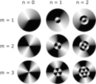
図6にパターン位相差層が有する位相差パターンの他の例を示す。図6において、左側の図は位相差パターンを位相で表す図であり、右側の図は位相差パターンの遅相軸分布の模式図である。図6は節が1(n=1)で次数が1~3(m=+1~+3)の場合の位相差パターンをそれぞれ示している。
図6の次数m=+1の図について説明する。
図6の左上に示すとおり、n=1、m=+1の位相差パターンは、半径方向に位相が非連続な節を有する。言い換えると、n=1、m=+1の位相差パターンは、円形の領域とこの領域の外側の円環状の領域を有しており、位相が0となる位置が互いに異なっている。具体的には、円形の領域においては、周方向に反時計回りに見た際に、位相が0の位置から周方向に1周する間に、位相が0から2πまで漸次、変化している。すなわち、円形の領域における位相変化は、節がない(n=0)場合の次数1(m=+1)の場合と同様である。一方、円環状の領域においては、周方向に反時計回りに見た際に、位相が0の位置から周方向に1周する間に、位相が0から2πまで漸次、変化しているが、位相が0の位置が円形の領域における位相0の位置から周方向に180°ズレている。すなわち、円環状の領域における位相変化は、節がない(n=0)場合の次数1(m=+1)の場合と同様である。
図6の左上に示すとおり、n=1、m=+1の位相差パターンは、半径方向に位相が非連続な節を有する。言い換えると、n=1、m=+1の位相差パターンは、円形の領域とこの領域の外側の円環状の領域を有しており、位相が0となる位置が互いに異なっている。具体的には、円形の領域においては、周方向に反時計回りに見た際に、位相が0の位置から周方向に1周する間に、位相が0から2πまで漸次、変化している。すなわち、円形の領域における位相変化は、節がない(n=0)場合の次数1(m=+1)の場合と同様である。一方、円環状の領域においては、周方向に反時計回りに見た際に、位相が0の位置から周方向に1周する間に、位相が0から2πまで漸次、変化しているが、位相が0の位置が円形の領域における位相0の位置から周方向に180°ズレている。すなわち、円環状の領域における位相変化は、節がない(n=0)場合の次数1(m=+1)の場合と同様である。
図6中右上に示される、このようなn=1、m=+1の位相差パターンの遅相軸分布の模式図から、半径方向に位相、すなわち、遅相軸の方向が非連続に変化していることがわかる。
図6の次数m=+2の図について説明する。
図6の左真ん中に示すとおり、n=1、m=+2の位相差パターンは、半径方向に位相が非連続な節を有する。言い換えると、n=1、m=+2の位相差パターンは、円形の領域とこの領域の外側の円環状の領域を有しており、位相が0となる位置が互いに異なっている。具体的には、円形の領域においては、周方向に反時計回りに見た際に、位相が0の位置から周方向に1周する間に、0から2πまでの位相変化を2回繰り返している。すなわち、円形の領域における位相変化は、節がない(n=0)場合の次数2(m=+2)の場合と同様である。一方、円環状の領域においては、周方向に反時計回りに見た際に、位相が0の位置から周方向に1周する間に、0から2πまでの位相変化を2回繰り返している。すなわち、円環状の領域における位相変化も、節がない(n=0)場合の次数2(m=+2)の場合と同様である。また、円形の領域と円環状の領域とでは、周方向における位相が0の位置が90°ズレている。
図6の左真ん中に示すとおり、n=1、m=+2の位相差パターンは、半径方向に位相が非連続な節を有する。言い換えると、n=1、m=+2の位相差パターンは、円形の領域とこの領域の外側の円環状の領域を有しており、位相が0となる位置が互いに異なっている。具体的には、円形の領域においては、周方向に反時計回りに見た際に、位相が0の位置から周方向に1周する間に、0から2πまでの位相変化を2回繰り返している。すなわち、円形の領域における位相変化は、節がない(n=0)場合の次数2(m=+2)の場合と同様である。一方、円環状の領域においては、周方向に反時計回りに見た際に、位相が0の位置から周方向に1周する間に、0から2πまでの位相変化を2回繰り返している。すなわち、円環状の領域における位相変化も、節がない(n=0)場合の次数2(m=+2)の場合と同様である。また、円形の領域と円環状の領域とでは、周方向における位相が0の位置が90°ズレている。
図6中右真ん中に示される、このようなn=1、m=+2の位相差パターンの遅相軸分布の模式図から、半径方向に位相、すなわち、遅相軸の方向が非連続に変化していることがわかる。
図6の次数m=+3の図について説明する。
図6の左下に示すとおり、n=1、m=+3の位相差パターンは、半径方向に位相が非連続な節を有する。言い換えると、n=1、m=+3の位相差パターンは、円形の領域とこの領域の外側の円環状の領域を有しており、位相が0となる位置が互いに異なっている。具体的には、円形の領域においては、周方向に反時計回りに見た際に、位相が0の位置から周方向に1周する間に、0から2πまでの位相変化を3回繰り返している。すなわち、円形の領域における位相変化は、節がない(n=0)場合の次数3(m=+3)の場合と同様である。一方、円環状の領域においては、周方向に反時計回りに見た際に、位相が0の位置から周方向に1周する間に、0から2πまでの位相変化を3回繰り返している。すなわち、円環状の領域における位相変化も、節がない(n=0)場合の次数3(m=+3)の場合と同様である。また、円形の領域と円環状の領域とでは、周方向における位相が0の位置が60°ズレている。
図6の左下に示すとおり、n=1、m=+3の位相差パターンは、半径方向に位相が非連続な節を有する。言い換えると、n=1、m=+3の位相差パターンは、円形の領域とこの領域の外側の円環状の領域を有しており、位相が0となる位置が互いに異なっている。具体的には、円形の領域においては、周方向に反時計回りに見た際に、位相が0の位置から周方向に1周する間に、0から2πまでの位相変化を3回繰り返している。すなわち、円形の領域における位相変化は、節がない(n=0)場合の次数3(m=+3)の場合と同様である。一方、円環状の領域においては、周方向に反時計回りに見た際に、位相が0の位置から周方向に1周する間に、0から2πまでの位相変化を3回繰り返している。すなわち、円環状の領域における位相変化も、節がない(n=0)場合の次数3(m=+3)の場合と同様である。また、円形の領域と円環状の領域とでは、周方向における位相が0の位置が60°ズレている。
図6中右下に示される、このようなn=1、m=+3の位相差パターンの遅相軸分布の模式図から、半径方向に位相、すなわち、遅相軸の方向が非連続に変化していることがわかる。
このように節を有する位相差パターンは、次数が同じであっても節の無い位相差パターンとは異なる状態の光渦を発生させることができる。従って、本発明の光通信システムが有するパターン位相差板は、節を有する位相差パターンを含んでいてもよい。
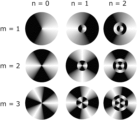
次に、節が2(n=2)の場合の位相差パターンの例について図7を用いて説明する。図7において、左側の図は位相差パターンを位相で表す図であり、右側の図は位相差パターンの遅相軸分布の模式図である。図7は節が2(n=2)で次数が1~3(m=+1~+3)の場合の位相差パターンをそれぞれ示している。
図7の次数m=+1の図について説明する。
図7の左上に示すとおり、n=2、m=+1の位相差パターンは、半径方向に位相が非連続な節を2つ有する。言い換えると、n=2、m=+1の位相差パターンは、円形の領域とこの領域の外側の2つの円環状の領域を有しており、隣り合う領域において位相が0となる位置が互いに異なっている。具体的には、円形の領域においては、周方向に反時計回りに見た際に、位相が0の位置から周方向に1周する間に、位相が0から2πまで漸次、変化している。すなわち、円形の領域における位相変化は、節がない(n=0)場合の次数1(m=+1)の場合と同様である。一方、円形の領域に接している1つ目の円環状の領域においては、周方向に反時計回りに見た際に、位相が0の位置から周方向に1周する間に、位相が0から2πまで漸次、変化している。すなわち、1つ目の円環状の領域における位相変化は、節がない(n=0)場合の次数1(m=+1)の場合と同様である。また、円形の領域と1つ目の円環状の領域とでは、周方向における位相が0の位置が180°ズレている。また、1つ目の円環状の領域の外側に接している2つ目の円環状の領域においては、周方向に反時計回りに見た際に、位相が0の位置から周方向に1周する間に、位相が0から2πまで漸次、変化している。すなわち、2つ目の円環状の領域における位相変化は、節がない(n=0)場合の次数1(m=+1)の場合と同様である。また、1つ目の円環状の領域と2つ目の円環状の領域とでは、周方向における位相が0の位置が180°ズレている。すなわち、隣接していない円形の領域と2つ目の円環状の領域とでは周方向における位相が0の位置が一致している。
図7の左上に示すとおり、n=2、m=+1の位相差パターンは、半径方向に位相が非連続な節を2つ有する。言い換えると、n=2、m=+1の位相差パターンは、円形の領域とこの領域の外側の2つの円環状の領域を有しており、隣り合う領域において位相が0となる位置が互いに異なっている。具体的には、円形の領域においては、周方向に反時計回りに見た際に、位相が0の位置から周方向に1周する間に、位相が0から2πまで漸次、変化している。すなわち、円形の領域における位相変化は、節がない(n=0)場合の次数1(m=+1)の場合と同様である。一方、円形の領域に接している1つ目の円環状の領域においては、周方向に反時計回りに見た際に、位相が0の位置から周方向に1周する間に、位相が0から2πまで漸次、変化している。すなわち、1つ目の円環状の領域における位相変化は、節がない(n=0)場合の次数1(m=+1)の場合と同様である。また、円形の領域と1つ目の円環状の領域とでは、周方向における位相が0の位置が180°ズレている。また、1つ目の円環状の領域の外側に接している2つ目の円環状の領域においては、周方向に反時計回りに見た際に、位相が0の位置から周方向に1周する間に、位相が0から2πまで漸次、変化している。すなわち、2つ目の円環状の領域における位相変化は、節がない(n=0)場合の次数1(m=+1)の場合と同様である。また、1つ目の円環状の領域と2つ目の円環状の領域とでは、周方向における位相が0の位置が180°ズレている。すなわち、隣接していない円形の領域と2つ目の円環状の領域とでは周方向における位相が0の位置が一致している。
図7中右上に示される、このようなn=2、m=+1の位相差パターンの遅相軸分布の模式図から、半径方向に位相、すなわち、遅相軸の方向が非連続に2回、変化していることがわかる。
図7の次数m=+2の図について説明する。
図7の左真ん中に示すとおり、n=2、m=+2の位相差パターンは、半径方向に位相が非連続な節を2つ有する。言い換えると、n=2、m=+2の位相差パターンは、円形の領域とこの領域の外側の2つの円環状の領域を有しており、隣り合う領域において位相が0となる位置が互いに異なっている。具体的には、円形の領域においては、周方向に反時計回りに見た際に、位相が0の位置から周方向に1周する間に、0から2πまでの位相変化を2回繰り返している。すなわち、円形の領域における位相変化は、節がない(n=0)場合の次数2(m=+2)の場合と同様である。一方、円形の領域に接している1つ目の円環状の領域においては、周方向に反時計回りに見た際に、位相が0の位置から周方向に1周する間に、0から2πまでの位相変化を2回繰り返している。すなわち、1つ目の円環状の領域における位相変化は、節がない(n=0)場合の次数2(m=+2)の場合と同様である。また、円形の領域と1つ目の円環状の領域とでは、周方向における位相が0の位置が90°ズレている。また、1つ目の円環状の領域の外側に接している2つ目の円環状の領域においては、周方向に反時計回りに見た際に、位相が0の位置から周方向に1周する間に、0から2πまでの位相変化を2回繰り返している。すなわち、2つ目の円環状の領域における位相変化は、節がない(n=0)場合の次数2(m=+2)の場合と同様である。また、1つ目の円環状の領域と2つ目の円環状の領域とでは、周方向における位相が0の位置が90°ズレている。すなわち、隣接していない円形の領域と2つ目の円環状の領域とでは周方向における位相が0の位置が一致している。
図7の左真ん中に示すとおり、n=2、m=+2の位相差パターンは、半径方向に位相が非連続な節を2つ有する。言い換えると、n=2、m=+2の位相差パターンは、円形の領域とこの領域の外側の2つの円環状の領域を有しており、隣り合う領域において位相が0となる位置が互いに異なっている。具体的には、円形の領域においては、周方向に反時計回りに見た際に、位相が0の位置から周方向に1周する間に、0から2πまでの位相変化を2回繰り返している。すなわち、円形の領域における位相変化は、節がない(n=0)場合の次数2(m=+2)の場合と同様である。一方、円形の領域に接している1つ目の円環状の領域においては、周方向に反時計回りに見た際に、位相が0の位置から周方向に1周する間に、0から2πまでの位相変化を2回繰り返している。すなわち、1つ目の円環状の領域における位相変化は、節がない(n=0)場合の次数2(m=+2)の場合と同様である。また、円形の領域と1つ目の円環状の領域とでは、周方向における位相が0の位置が90°ズレている。また、1つ目の円環状の領域の外側に接している2つ目の円環状の領域においては、周方向に反時計回りに見た際に、位相が0の位置から周方向に1周する間に、0から2πまでの位相変化を2回繰り返している。すなわち、2つ目の円環状の領域における位相変化は、節がない(n=0)場合の次数2(m=+2)の場合と同様である。また、1つ目の円環状の領域と2つ目の円環状の領域とでは、周方向における位相が0の位置が90°ズレている。すなわち、隣接していない円形の領域と2つ目の円環状の領域とでは周方向における位相が0の位置が一致している。
図7中右真ん中に示される、このようなn=2、m=+2の位相差パターンの遅相軸分布の模式図から、半径方向に位相、すなわち、遅相軸の方向が非連続に2回、変化していることがわかる。
図7の次数m=+3の図について説明する。
図7の左下に示すとおり、n=2、m=+3の位相差パターンは、半径方向に位相が非連続な節を2つ有する。言い換えると、n=2、m=+3の位相差パターンは、円形の領域とこの領域の外側の2つの円環状の領域を有しており、隣り合う領域において位相が0となる位置が互いに異なっている。具体的には、円形の領域においては、周方向に反時計回りに見た際に、位相が0の位置から周方向に1周する間に、0から2πまでの位相変化を3回繰り返している。すなわち、円形の領域における位相変化は、節がない(n=0)場合の次数3(m=+3)の場合と同様である。一方、円形の領域に接している1つ目の円環状の領域においては、周方向に反時計回りに見た際に、位相が0の位置から周方向に1周する間に、0から2πまでの位相変化を3回繰り返している。すなわち、1つ目の円環状の領域における位相変化は、節がない(n=0)場合の次数3(m=+3)の場合と同様である。また、円形の領域と1つ目の円環状の領域とでは、周方向における位相が0の位置が60°ズレている。また、1つ目の円環状の領域の外側に接している2つ目の円環状の領域においては、周方向に反時計回りに見た際に、位相が0の位置から周方向に1周する間に、0から2πまでの位相変化を3回繰り返している。すなわち、2つ目の円環状の領域における位相変化は、節がない(n=0)場合の次数3(m=+3)の場合と同様である。また、1つ目の円環状の領域と2つ目の円環状の領域とでは、周方向における位相が0の位置が60°ズレている。すなわち、隣接していない円形の領域と2つ目の円環状の領域とでは周方向における位相が0の位置が一致している。
図7の左下に示すとおり、n=2、m=+3の位相差パターンは、半径方向に位相が非連続な節を2つ有する。言い換えると、n=2、m=+3の位相差パターンは、円形の領域とこの領域の外側の2つの円環状の領域を有しており、隣り合う領域において位相が0となる位置が互いに異なっている。具体的には、円形の領域においては、周方向に反時計回りに見た際に、位相が0の位置から周方向に1周する間に、0から2πまでの位相変化を3回繰り返している。すなわち、円形の領域における位相変化は、節がない(n=0)場合の次数3(m=+3)の場合と同様である。一方、円形の領域に接している1つ目の円環状の領域においては、周方向に反時計回りに見た際に、位相が0の位置から周方向に1周する間に、0から2πまでの位相変化を3回繰り返している。すなわち、1つ目の円環状の領域における位相変化は、節がない(n=0)場合の次数3(m=+3)の場合と同様である。また、円形の領域と1つ目の円環状の領域とでは、周方向における位相が0の位置が60°ズレている。また、1つ目の円環状の領域の外側に接している2つ目の円環状の領域においては、周方向に反時計回りに見た際に、位相が0の位置から周方向に1周する間に、0から2πまでの位相変化を3回繰り返している。すなわち、2つ目の円環状の領域における位相変化は、節がない(n=0)場合の次数3(m=+3)の場合と同様である。また、1つ目の円環状の領域と2つ目の円環状の領域とでは、周方向における位相が0の位置が60°ズレている。すなわち、隣接していない円形の領域と2つ目の円環状の領域とでは周方向における位相が0の位置が一致している。
図7中右下に示される、このようなn=2、m=+3の位相差パターンの遅相軸分布の模式図から、半径方向に位相、すなわち、遅相軸の方向が非連続に2回、変化していることがわかる。
このように節の数および/または次数が異なる位相差パターンは、互いに異なる状態の光渦を発生させることができる。従って、本発明の光通信システムが有するパターン位相差板は、節の数および/または次数が異なる位相差パターンを含んでいてもよい。
節の数は0~2に限定はされず、3以上であってもよい。また、前述のとおり、次数も0~±3に限定はされず、+4以上あるいは-4以下であってもよい。一例として、n=2~5で、m=+3~+5の場合の位相差パターンを図8に示す。各位相差パターンは、互いに異なる光渦を発生させることができる。
[パターン位相差板]
本発明のパターン位相差板は、入射する偏光を光渦に変換する位相差パターンを複数有するものであって、次数の異なる複数の位相差パターンを同一面内に有する、パターン位相差板である。
本発明のパターン位相差板は、入射する偏光を光渦に変換する位相差パターンを複数有するものであって、次数の異なる複数の位相差パターンを同一面内に有する、パターン位相差板である。
パターン位相差板が有する位相差パターンは、上述のとおりであり、パターン位相差板は、節の数および/または次数が異なる位相差パターンを同一面内に有する。
パターン位相差板における位相差パターンの配列については特に制限はない。例えば、節n=0、次数m=0~+3の4種の位相差パターンを次数の順に一方向に配列した構成とすることができる。
次に、位相差パターンの形成方法について説明する。
本発明において、位相差パターンの形成方法には特に制限はない。
パターン位相差板が、液晶化合物を所定の配向状態に配向してなる液晶層である場合には、液晶化合物を含む液晶組成物を、液晶化合物を所定の位相差パターンに配向するための配向膜上に塗布して、液晶化合物由来の光学軸の向きを位相差パターンに配向した液晶相を形成し、これを層状に固定して形成できる。
また、本発明において、液晶層は、多層塗布による形成されてもよい。多層塗布とは、先ず配向膜の上に1層目の液晶組成物を塗布、加熱、冷却後に紫外線硬化を行って液晶固定化層を作製した後、2層目以降はその液晶固定化層に重ね塗りして塗布を行い、同様に加熱、冷却後に紫外線硬化を行うことを、所望の厚みになるまで繰り返して、液晶層を形成する方法である。
(配向膜)
配向膜は、液晶層を形成する際に、液晶化合物を所定の位相差パターンに配向するための配向膜である。
配向膜は、液晶層を形成する際に、液晶化合物を所定の位相差パターンに配向するための配向膜である。
配向膜は、光配向性の素材に偏光または非偏光を照射して配向膜とした、いわゆる光配向膜が好適に利用される。すなわち、本発明においては、配向膜として、例えば支持体上に、光配向材料を塗布して形成した光配向膜が、好適に利用される。
偏光の照射は、光配向膜に対して、垂直方向または斜め方向から行うことができ、非偏光の照射は、光配向膜に対して、斜め方向から行うことができる。
偏光の照射は、光配向膜に対して、垂直方向または斜め方向から行うことができ、非偏光の照射は、光配向膜に対して、斜め方向から行うことができる。
本発明に利用可能な配向膜に用いられる光配向材料としては、例えば、特開2006-285197号公報、特開2007-76839号公報、特開2007-138138号公報、特開2007-94071号公報、特開2007-121721号公報、特開2007-140465号公報、特開2007-156439号公報、特開2007-133184号公報、特開2009-109831号公報、特許第3883848号公報および特許第4151746号公報に記載のアゾ化合物、特開2002-229039号公報に記載の芳香族エステル化合物、特開2002-265541号公報および特開2002-317013号公報に記載の光配向性単位を有するマレイミドおよび/またはアルケニル置換ナジイミド化合物、特許第4205195号および特許第4205198号に記載の光架橋性シラン誘導体、特表2003-520878号公報、特表2004-529220号公報および特許第4162850号に記載の光架橋性ポリイミド、光架橋性ポリアミドおよび光架橋性ポリエステル、ならびに、特開平9-118717号公報、特表平10-506420号公報、特表2003-505561号公報、国際公開第2010/150748号、特開2013-177561号公報および特開2014-12823号公報に記載の光二量化可能な化合物、特にシンナメート化合物、カルコン化合物およびクマリン化合物等が、好ましい例として例示される。
中でも、アゾ化合物、光架橋性ポリイミド、光架橋性ポリアミド、光架橋性ポリエステル、シンナメート化合物、および、カルコン化合物は、好適に利用される。
中でも、アゾ化合物、光架橋性ポリイミド、光架橋性ポリアミド、光架橋性ポリエステル、シンナメート化合物、および、カルコン化合物は、好適に利用される。
配向膜の厚さには、制限はなく、配向膜の形成材料に応じて、必要な配向機能を得られる厚さを、適宜、設定すればよい。
配向膜の厚さは、0.01~5μmが好ましく、0.05~2μmがより好ましい。
配向膜の厚さは、0.01~5μmが好ましく、0.05~2μmがより好ましい。
本発明において、配向パターンを形成するための配向膜の好適な露光方法としては、配向膜を直接描画法で露光する方法、および、異なる露光パターンを有するマスクを用いて複数回、偏光露光する方法、が挙げられる。
直接描画法は、配向膜を有する支持体をXYステージ上に配置し、直線偏光された光ビームをλ/2板を通して、配向膜上に合焦させて、XYステージを移動させることで、合焦位置を走査し、また、λ/2板を回転させることで、直線偏光の偏光方向を任意の方向に変換することで、配向膜に所望の配向パターンを描画するものである。
λ/2板の回転、および、XYステージの移動は、例えば、コンピュータにより制御されて、配向膜表面の、光が合焦される位置と、光の偏光方向とを対応させることで、配向膜上に所望の配向パターンを形成することができる。
λ/2板の回転、および、XYステージの移動は、例えば、コンピュータにより制御されて、配向膜表面の、光が合焦される位置と、光の偏光方向とを対応させることで、配向膜上に所望の配向パターンを形成することができる。
照射する光の強度、露光時間等は、配向膜の形成材料等に応じて適宜設定すればよい。
単位面積あたりの露光量は、照射する光の強度と走査速度で調整することができる。配向膜に配向性を与えるために十分な露光を行う観点から、100mJ/m2以上であることが好ましく、150mJ/m2であることがより好ましい。また、過剰な照射による配向性低下を防ぐ観点から、5J/m2以下であることが好ましく、3J/m2以下であることがより好ましい。
また、配向膜上において合焦される光ビームのスポット径は、所望の配向パターンを配向膜に付与することができる大きさであればよい。
単位面積あたりの露光量は、照射する光の強度と走査速度で調整することができる。配向膜に配向性を与えるために十分な露光を行う観点から、100mJ/m2以上であることが好ましく、150mJ/m2であることがより好ましい。また、過剰な照射による配向性低下を防ぐ観点から、5J/m2以下であることが好ましく、3J/m2以下であることがより好ましい。
また、配向膜上において合焦される光ビームのスポット径は、所望の配向パターンを配向膜に付与することができる大きさであればよい。
以下、異なる露光パターンを有するマスクを用いて複数回、偏光露光する方法(以下、多重偏光露光法ともいう)について説明する。
多重偏光露光法は、光配向膜に例えば、3回の偏光露光を行う工程を有し、3回の偏光露光において、照射光量パターンを互いに異なるものとし、かつ、照射する直線偏光の偏光方向を互いに異なるものとする、露光方法である。
多重偏光露光法の一例を図9~図11を用いて説明する。
多重偏光露光法の一例を図9~図11を用いて説明する。
図9の上の図は、1回目の偏光露光に用いられるマスクを概念的に表す図であり、図9の下の図は、1回目の偏光露光で照射される直線偏光の偏光方向を示す矢印である。
また、図10の上の図は、2回目の偏光露光に用いられるマスクを概念的に表す図であり、図10の下の図は、2回目の偏光露光で照射される直線偏光の偏光方向を示す矢印である。
また、図11の上の図は、3回目の偏光露光に用いられるマスクを概念的に表す図であり、図11の下の図は、3回目の偏光露光で照射される直線偏光の偏光方向を示す矢印である。
図9~図11の上に示す図は、各偏光露光で用いるマスクの透過率を、透過率が高い(例えば、100%の)領域を白、低い(例えば、0%の)領域を黒としてグレースケールで表した図である。
また、図10の上の図は、2回目の偏光露光に用いられるマスクを概念的に表す図であり、図10の下の図は、2回目の偏光露光で照射される直線偏光の偏光方向を示す矢印である。
また、図11の上の図は、3回目の偏光露光に用いられるマスクを概念的に表す図であり、図11の下の図は、3回目の偏光露光で照射される直線偏光の偏光方向を示す矢印である。
図9~図11の上に示す図は、各偏光露光で用いるマスクの透過率を、透過率が高い(例えば、100%の)領域を白、低い(例えば、0%の)領域を黒としてグレースケールで表した図である。
図9~図11に示すように、1~3回目の偏光露光に用いるマスクはいずれも、透過率が最も高い位置から、周方向に180°の位置で透過率が最も低くなり、その間では透過率が漸次変化する透過率パターンを有している。また、1~3回目の偏光露光に用いるマスクは、透過率が最も高くなる位置が周方向に互いにズレている。具体的には、2回目のマスクの透過率が最も高くなる位置は、1回目のマスクの透過率が最も高くなる位置から周方向に120°ズレている。また、3回目のマスクの透過率が最も高くなる位置は、1回目のマスクの透過率が最も高くなる位置から周方向に240°(2回目のマスクに対して120°)ズレている。
また、図9に示すように、1回目の偏光露光に用いる直線偏光の偏光方向は、1回目のマスクの透過率が最も高くなる方向(図中右方向)に対して直交している。
また、図9および図10に示すように、2回目の偏光露光に用いる直線偏光の偏光方向は、1回目の直線偏光の偏光方向と反時計回りに60°ズレている。
また、図9および図11に示すように、3回目の偏光露光に用いる直線偏光の偏光方向は、1回目の直線偏光の偏光方向と時計回りに60°(-60°)ズレている。すなわち、3回目の偏光露光に用いる直線偏光の偏光方向は、2回目の直線偏光の偏光方向と時計回りに120°(-120°)ズレている。
また、図9および図10に示すように、2回目の偏光露光に用いる直線偏光の偏光方向は、1回目の直線偏光の偏光方向と反時計回りに60°ズレている。
また、図9および図11に示すように、3回目の偏光露光に用いる直線偏光の偏光方向は、1回目の直線偏光の偏光方向と時計回りに60°(-60°)ズレている。すなわち、3回目の偏光露光に用いる直線偏光の偏光方向は、2回目の直線偏光の偏光方向と時計回りに120°(-120°)ズレている。
偏光方向が異なる直線偏光を用いて複数回の偏光露光を行うと、露光量に応じて平均化した配向規制力が生じる。そのため、このようなマスクおよび直線偏光を用いて複数回の偏光露光を行うことにより、各偏光露光の露光量の比率が配向膜の面内の位置ごとに変わり、配向膜の位置ごとに、配向規制力の方向が変わる。
例えば、アゾ系の光配向膜を用いた場合には、照射した直線偏光の偏光方向と直交する方向に配向規制力が生じる。そのため、方位0°の方向(図中右側)の位置においては、1回目のマスクの透過率が高く、2回目および3回目のマスクの透過率が1回目のマスクの透過率よりも低く略同じであるため、1回目~3回目の偏光方向を重ね合わせると、図中上下方向の直線偏光に露光された状態となり、これに直交する方向(左右方向)に配向規制力が生じる。また、方位180°の方向(図中左側)の位置においては、1回目のマスクの透過率が低く、2回目および3回目のマスクの透過率が1回目よりも高く略同じであるため、1回目~3回目の偏光方向を重ね合わせると、図中左右方向の直線偏光に露光された状態となり、図中上下方向に配向規制力が生じる。
このように、配向膜の面内の位置ごとに配向規制力の方向が変わり、ある1点を中心に1周したときの遅相軸の方位角が変化する位相差パターンを形成するための配向パターンを形成することができる。
このように、配向膜の面内の位置ごとに配向規制力の方向が変わり、ある1点を中心に1周したときの遅相軸の方位角が変化する位相差パターンを形成するための配向パターンを形成することができる。
図9~図11に示す例の場合には、図2に示す次数m=+1の位相差パターンを形成するための配向パターンを配向膜に形成することができる。
なお、偏光露光の順番が上記に限定はされず、マスクおよび異なる偏光を用いた偏光露光を3回行えば、上記と異なる順番でも所望の配向パターンを得ることができる。
また、光配向膜の種類によっては、偏光露光の偏光方向と液晶の配向方向が同じになる場合がある。その場合は、それに合わせて各露光マスクパターンを同じ角度だけ適宜回転させることで、所望の配向パターンを得ることができる。
また、上記説明では、3回の偏光露光を行うとしたが、所望の配向パターンを得ることができれば、これに限定はされず、4回以上の偏光露光を行ってもよい。
また、各偏光露光で用いるマスクの透過率の分布、および、照射する直線偏光の偏光方向は、所望の配向パターンを得ることができれば、上記例に限定はされない。各偏光露光で用いるマスクの透過率の分布、および、照射する直線偏光の偏光方向は、所望の配向パターンに応じて適宜、設定すればよい。
図12~図14に、節n=0~2、次数m=+1~+3の各位相差パターンを形成するための配向パターンを形成するためのマスクの透過率を概念的に表す図を示す。
図12に示すマスクを用いる際には、図に示すマスクに対して偏向方向が上下方向となる直線偏光を用い(図9参照)、図13に示すマスクを用いる際には、図に示すマスクの上下方向に対して偏向方向が反時計回りに60°傾いている直線偏光を用い(図10参照)、図14に示すマスクを用いる際には、図に示すマスクの上下方向に対して偏向方向が時計回りに60°(-60°)傾いている直線偏光を用いる(図11参照)。
図12~図14に示すマスクを用いて偏光露光を3回行うことにより、図5~図7に示す各位相差パターンを形成することができる。
ここで、多重偏光露光法による配向パターンの形成は、透過率のパターンが異なるマスクを面内方向に配列して同じ直線偏光を用いて偏光露光を行うことができるため、1つの配向膜の同一面内上に異なる配向パターンを容易に形成することができる点で有利である。
例えば、節n=0、次数m=+1~+3の位相差パターンに対応する配向パターンを1つの配向膜に形成する場合に、図9および図12に示す節n=0、次数m=+1~+3に対応する透過率のパターンを面内に配列して有するマスクを用いて1回目の偏光露光を行い、図10および図13に示す節n=0、次数m=+1~+3に対応する透過率のパターンを面内に配列して有するマスクを用いて2回目の偏光露光を行い、図11および図14に示す節n=0、次数m=+1~+3に対応する透過率のパターンを面内に配列して有するマスクを用いて3回目の偏光露光を行うことで、1つの配向膜に節n=0、次数m=+1~+3の位相差パターンに対応する配向パターンを形成することができる。このような複数の配向パターンを有する配向膜上に液晶層を形成することで、次数が異なる位相差パターンを同一面内に有するパターン位相差板を作製することができる。
例えば、節n=0、次数m=+1~+3の位相差パターンに対応する配向パターンを1つの配向膜に形成する場合に、図9および図12に示す節n=0、次数m=+1~+3に対応する透過率のパターンを面内に配列して有するマスクを用いて1回目の偏光露光を行い、図10および図13に示す節n=0、次数m=+1~+3に対応する透過率のパターンを面内に配列して有するマスクを用いて2回目の偏光露光を行い、図11および図14に示す節n=0、次数m=+1~+3に対応する透過率のパターンを面内に配列して有するマスクを用いて3回目の偏光露光を行うことで、1つの配向膜に節n=0、次数m=+1~+3の位相差パターンに対応する配向パターンを形成することができる。このような複数の配向パターンを有する配向膜上に液晶層を形成することで、次数が異なる位相差パターンを同一面内に有するパターン位相差板を作製することができる。
(液晶層)
液晶層は、配向膜の表面に形成される。
上述したように、液晶層は、液晶化合物を配向した液晶相を固定してなる、液晶層であり、位相差パターンを有する液晶層である。
液晶層は、配向膜の表面に形成される。
上述したように、液晶層は、液晶化合物を配向した液晶相を固定してなる、液晶層であり、位相差パターンを有する液晶層である。
<<液晶層の形成方法>>
液晶層は、液晶化合物を位相差パターンに配向した液晶相を層状に固定して形成できる。
液晶相を固定した構造は、液晶相となっている液晶化合物の配向が保持されている構造であればよく、典型的には、重合性液晶化合物を位相差パターンに沿った配向状態としたうえで、紫外線照射、加熱等によって重合、硬化し、流動性が無い層を形成して、同時に、外場または外力によって配向形態に変化を生じさせることない状態に変化した構造が好ましい。
なお、液晶相を固定した構造においては、液晶相の光学的性質が保持されていれば十分であり、液晶層において、液晶化合物は液晶性を示さなくてもよい。例えば、重合性液晶化合物は、硬化反応により高分子量化して、液晶性を失っていてもよい。
液晶相を固定してなる液晶層の形成に用いる材料としては、一例として、液晶化合物を含む液晶組成物が挙げられる。液晶化合物は重合性液晶化合物であるのが好ましい。
また、液晶層の形成に用いる液晶組成物は、さらに界面活性剤、重合開始剤等を含んでいてもよい。
また、液晶層の形成に用いる液晶組成物は、さらに界面活性剤、重合開始剤等を含んでいてもよい。
--重合性液晶化合物--
重合性液晶化合物は、棒状液晶化合物であっても、円盤状液晶化合物であってもよい。
液晶層を形成する棒状の重合性液晶化合物の例としては、棒状ネマチック液晶化合物が挙げられる。棒状ネマチック液晶化合物としては、アゾメチン類、アゾキシ類、シアノビフェニル類、シアノフェニルエステル類、安息香酸エステル類、シクロヘキサンカルボン酸フェニルエステル類、シアノフェニルシクロヘキサン類、シアノ置換フェニルピリミジン類、アルコキシ置換フェニルピリミジン類、フェニルジオキサン類、トラン類、および、アルケニルシクロヘキシルベンゾニトリル類等が好ましく用いられる。低分子液晶化合物だけではなく、高分子液晶化合物も用いることができる。
棒状液晶化合物を重合によって配向を固定することがより好ましく、重合性棒状液晶化合物としては、Makromol. Chem., 190巻、2255頁(1989年)、Advanced Materials 5巻、107頁(1993年)、米国特許4683327号明細書、同5622648号明細書、同5770107号明細書、国際公開第95/22586号、同95/24455号、同97/00600号、同98/23580号、同98/52905号、特開平1-272551号公報、同6-16616号公報、同7-110469号公報、同11-80081号公報、および、特願2001-64627号公報などに記載の化合物を用いることができる。さらに棒状液晶化合物としては、例えば、特表平11-513019号公報および特開2007-279688号公報に記載のものも好ましく用いることができる。また、2種類以上の重合性液晶化合物を併用してもよい。2種類以上の重合性液晶化合物を併用すると、配向温度を低下させることができる。
重合性基の例には、不飽和重合性基、エポキシ基、およびアジリジニル基が含まれ、不飽和重合性基が好ましく、エチレン性不飽和重合性基がより好ましい。重合性基は種々の方法で、液晶化合物の分子中に導入できる。重合性液晶化合物が有する重合性基の個数は、好ましくは1~6個、より好ましくは1~3個である。
また、上記以外の重合性液晶化合物としては、特開昭57-165480号公報に開示されているようなコレステリック相を有する環式オルガノポリシロキサン化合物等を用いることができる。さらに、前述の高分子液晶化合物としては、液晶を呈するメソゲン基を主鎖、側鎖、あるいは主鎖および側鎖の両方の位置に導入した高分子、コレステリル基を側鎖に導入した高分子コレステリック液晶、特開平9-133810号公報に開示されているような液晶性高分子、および、特開平11-293252号公報に開示されているような液晶性高分子等を用いることができる。
--円盤状液晶化合物--
円盤状液晶化合物としては、例えば、特開2007-108732号公報や特開2010-244038号公報に記載のものを好ましく用いることができる。
なお、液晶層に円盤状液晶化合物を用いた場合には、液晶層において、液晶化合物は厚さ方向に立ち上がっており、液晶化合物に由来する光学軸は、円盤面に垂直な軸、いわゆる進相軸として定義される。
円盤状液晶化合物としては、例えば、特開2007-108732号公報や特開2010-244038号公報に記載のものを好ましく用いることができる。
なお、液晶層に円盤状液晶化合物を用いた場合には、液晶層において、液晶化合物は厚さ方向に立ち上がっており、液晶化合物に由来する光学軸は、円盤面に垂直な軸、いわゆる進相軸として定義される。
また、液晶組成物中の重合性液晶化合物の添加量は、液晶組成物の固形分質量(溶媒を除いた質量)に対して、75~99.9質量%であるのが好ましく、80~99質量%であるのがより好ましく、85~90質量%であるのがさらに好ましい。
液晶化合物としては、高い回折効率を得るために、屈折率異方性Δnの高い液晶化合物を好ましく用いることができる。
--界面活性剤--
液晶層を形成する際に用いる液晶組成物は、界面活性剤を含有してもよい。
界面活性剤は、安定的に、または迅速に、液晶化合物の配向に寄与する配向制御剤として機能できる化合物が好ましい。界面活性剤としては、例えば、シリコ-ン系界面活性剤およびフッ素系界面活性剤が挙げられ、フッ素系界面活性剤が好ましく例示される。
液晶層を形成する際に用いる液晶組成物は、界面活性剤を含有してもよい。
界面活性剤は、安定的に、または迅速に、液晶化合物の配向に寄与する配向制御剤として機能できる化合物が好ましい。界面活性剤としては、例えば、シリコ-ン系界面活性剤およびフッ素系界面活性剤が挙げられ、フッ素系界面活性剤が好ましく例示される。
界面活性剤の具体例としては、特開2014-119605号公報の段落[0082]~[0090]に記載の化合物、特開2012-203237号公報の段落[0031]~[0034]に記載の化合物、特開2005-99248号公報の段落[0092]および[0093]中に例示されている化合物、特開2002-129162号公報の段落[0076]~[0078]および段落[0082]~[0085]中に例示されている化合物、ならびに、特開2007-272185号公報の段落[0018]~[0043]等に記載のフッ素(メタ)アクリレート系ポリマー、などが挙げられる。
なお、界面活性剤は、1種を単独で用いてもよいし、2種以上を併用してもよい。
フッ素系界面活性剤として、特開2014-119605号公報の段落[0082]~[0090]に記載の化合物が好ましい。
なお、界面活性剤は、1種を単独で用いてもよいし、2種以上を併用してもよい。
フッ素系界面活性剤として、特開2014-119605号公報の段落[0082]~[0090]に記載の化合物が好ましい。
液晶組成物中における、界面活性剤の添加量は、液晶化合物の全質量に対して0.01~10質量%が好ましく、0.01~5質量%がより好ましく、0.02~2質量%がさらに好ましい。
--重合開始剤--
液晶組成物が重合性化合物を含む場合は、重合開始剤を含有しているのが好ましい。紫外線照射により重合反応を進行させる態様では、使用する重合開始剤は、紫外線照射によって重合反応を開始可能な光重合開始剤であるのが好ましい。
光重合開始剤の例には、α-カルボニル化合物(米国特許第2367661号、米国特許第2367670号の各明細書記載)、アシロインエーテル(米国特許第2448828号明細書記載)、α-炭化水素置換芳香族アシロイン化合物(米国特許第2722512号明細書記載)、多核キノン化合物(米国特許第3046127号、米国特許第2951758号の各明細書記載)、トリアリールイミダゾールダイマーとp-アミノフェニルケトンとの組み合わせ(米国特許第3549367号明細書記載)、アクリジンおよびフェナジン化合物(特開昭60-105667号公報、米国特許第4239850号明細書記載)、ならびに、オキサジアゾール化合物(米国特許第4212970号明細書記載)等が挙げられる。
液晶組成物中の光重合開始剤の含有量は、液晶化合物の含有量に対して0.1~20質量%であるのが好ましく、0.5~12質量%であるのがさらに好ましい。
--架橋剤--
液晶組成物は、硬化後の膜強度向上、耐久性向上のため、任意に架橋剤を含有していてもよい。架橋剤としては、紫外線、熱、および、湿気等で硬化するものが好適に使用できる。
架橋剤としては、特に制限はなく、目的に応じて適宜選択することができ、例えばトリメチロールプロパントリ(メタ)アクリレートおよびペンタエリスリトールトリ(メタ)アクリレート等の多官能アクリレート化合物;グリシジル(メタ)アクリレートおよびエチレングリコールジグリシジルエーテル等のエポキシ化合物;2,2-ビスヒドロキシメチルブタノール-トリス[3-(1-アジリジニル)プロピオネート]および4,4-ビス(エチレンイミノカルボニルアミノ)ジフェニルメタン等のアジリジン化合物;ヘキサメチレンジイソシアネートおよびビウレット型イソシアネート等のイソシアネート化合物;オキサゾリン基を側鎖に有するポリオキサゾリン化合物;ならびに、ビニルトリメトキシシラン、N-(2-アミノエチル)3-アミノプロピルトリメトキシシラン等のアルコキシシラン化合物などが挙げられる。また、架橋剤の反応性に応じて公知の触媒を用いることができ、膜強度および耐久性向上に加えて生産性を向上させることができる。これらは、1種単独で使用してもよいし、2種以上を併用してもよい。
架橋剤の含有量は、液晶組成物の固形分質量に対して、3~20質量%が好ましく、5~15質量%がより好ましい。架橋剤の含有量が上記範囲内であれば、架橋密度向上の効果が得られやすく、液晶相の安定性がより向上する。
--その他の添加剤--
液晶組成物中には、必要に応じて、さらに重合禁止剤、酸化防止剤、紫外線吸収剤、光安定化剤、色材、および、金属酸化物微粒子等を、光学的性能等を低下させない範囲で添加することができる。
液晶組成物中には、必要に応じて、さらに重合禁止剤、酸化防止剤、紫外線吸収剤、光安定化剤、色材、および、金属酸化物微粒子等を、光学的性能等を低下させない範囲で添加することができる。
液晶組成物は、液晶層を形成する際には、液体として用いられるのが好ましい。
液晶組成物は溶媒を含んでいてもよい。溶媒には、制限はなく、目的に応じて適宜選択することができるが、有機溶媒が好ましい。
有機溶媒には、制限はなく、目的に応じて適宜選択することができ、例えば、ケトン類、アルキルハライド類、アミド類、スルホキシド類、ヘテロ環化合物、炭化水素類、エステル類、および、エーテル類などが挙げられる。これらは、1種単独で使用してもよいし、2種以上を併用してもよい。これらの中でも、環境への負荷を考慮した場合にはケトン類が好ましい。
液晶組成物は溶媒を含んでいてもよい。溶媒には、制限はなく、目的に応じて適宜選択することができるが、有機溶媒が好ましい。
有機溶媒には、制限はなく、目的に応じて適宜選択することができ、例えば、ケトン類、アルキルハライド類、アミド類、スルホキシド類、ヘテロ環化合物、炭化水素類、エステル類、および、エーテル類などが挙げられる。これらは、1種単独で使用してもよいし、2種以上を併用してもよい。これらの中でも、環境への負荷を考慮した場合にはケトン類が好ましい。
液晶層を形成する際には、液晶層の形成面に液晶組成物を塗布して、液晶化合物を所定の液晶配向パターンに配向された液晶相の状態に配向した後、液晶化合物を硬化して、液晶層とするのが好ましい。
すなわち、配向膜上に液晶層を形成する場合には、配向膜に液晶組成物を塗布して、液晶化合物を所定の液晶配向パターンに配向した後、液晶化合物を硬化して、液晶相を固定してなる液晶層を形成するのが好ましい。
液晶組成物の塗布は、インクジェットおよびスクロール印刷等の印刷法、ならびに、スピンコート、バーコートおよびスプレー塗布等のシート状物に液体を一様に塗布できる公知の方法が全て利用可能である。
すなわち、配向膜上に液晶層を形成する場合には、配向膜に液晶組成物を塗布して、液晶化合物を所定の液晶配向パターンに配向した後、液晶化合物を硬化して、液晶相を固定してなる液晶層を形成するのが好ましい。
液晶組成物の塗布は、インクジェットおよびスクロール印刷等の印刷法、ならびに、スピンコート、バーコートおよびスプレー塗布等のシート状物に液体を一様に塗布できる公知の方法が全て利用可能である。
塗布された液晶組成物は、必要に応じて乾燥および/または加熱され、その後、硬化され、液晶層を形成する。この乾燥および/または加熱の工程で、液晶組成物中の液晶化合物が所定の液晶配向パターンに配向すればよい。加熱を行う場合、加熱温度は、200℃以下が好ましく、130℃以下がより好ましい。
配向させた液晶化合物は、必要に応じて、さらに重合される。重合は、熱重合、および、光照射による光重合のいずれでもよいが、光重合が好ましい。光照射は、紫外線を用いるのが好ましい。照射エネルギーは、20mJ/cm2~50J/cm2が好ましく、50~1500mJ/cm2がより好ましい。光重合反応を促進するため、加熱条件下または窒素雰囲気下で光照射を実施してもよい。照射する紫外線の波長は250~430nmが好ましい。
液晶層の厚さには、制限はなく、液晶層の用途、および、液晶層の形成材料等に応じて、適宜、設定すればよい。
液晶層において、微小な領域における面内レタデーション(Re)の値は、光通信システムの光源が出射する光の波長(例えば、近赤外光)に対して、半波長すなわちλ/2であるのが好ましい。面内レタデーションは、領域内の屈折率異方性に伴う屈折率差Δnと液晶層の厚さとの積により算出される。ここで、液晶層における領域の屈折率異方性に伴う屈折率差とは、領域の面内における遅相軸の方向の屈折率と、遅相軸の方向に直交する方向の屈折率との差により定義される屈折率差である。すなわち、領域の屈折率異方性に伴う屈折率差Δnは、領域の面内において、光学軸の方向の液晶化合物の屈折率と、光学軸に垂直な方向の液晶化合物の屈折率との差に等しい。つまり、屈折率差Δnは、液晶化合物の屈折率差に等しい。
なお、いわゆるλ/2板として機能するのは液晶層であるが、本発明においては、支持体および配向膜を一体的に備えた積層体がλ/2板として機能する態様を含む。
以上、本発明の光通信システムおよびパターン位相差板について詳細に説明したが、本発明は上述の例に限定はされず、本発明の要旨を逸脱しない範囲において、各種の改良や変更を行ってもよいのは、もちろんである。
以下に実施例を挙げて本発明の特徴をさらに具体的に説明する。
以下の実施例に示す材料、試薬、使用量、物質量、割合、処理内容、および、処理手順等は、本発明の趣旨を逸脱しない限り適宜変更することができる。したがって、本発明の範囲は以下に示す具体例により限定的に解釈されるべきものではない。
以下の実施例に示す材料、試薬、使用量、物質量、割合、処理内容、および、処理手順等は、本発明の趣旨を逸脱しない限り適宜変更することができる。したがって、本発明の範囲は以下に示す具体例により限定的に解釈されるべきものではない。
[実施例1]
<液晶層の作製>
(支持体)
支持体として、平板状のガラス基板を用意した。
<液晶層の作製>
(支持体)
支持体として、平板状のガラス基板を用意した。
(配向膜の形成)
支持体上に、下記の配向膜形成用塗布液をスピンコートで塗布した。この配向膜形成用塗布液の塗膜が形成された支持体を60℃のホットプレート上で60秒間乾燥し、配向膜を形成した。
支持体上に、下記の配向膜形成用塗布液をスピンコートで塗布した。この配向膜形成用塗布液の塗膜が形成された支持体を60℃のホットプレート上で60秒間乾燥し、配向膜を形成した。
配向膜形成用塗布液
――――――――――――――――――――――――――――――――
光配向用素材A 1.00質量部
水 16.00質量部
ブトキシエタノール 42.00質量部
プロピレングリコールモノメチルエーテル 42.00質量部
――――――――――――――――――――――――――――――――
――――――――――――――――――――――――――――――――
光配向用素材A 1.00質量部
水 16.00質量部
ブトキシエタノール 42.00質量部
プロピレングリコールモノメチルエーテル 42.00質量部
――――――――――――――――――――――――――――――――
-光配向用素材A-

(配向膜の露光)
以下のように配向膜に対して偏光露光を3回行うことにより、配向膜に配向パターンを形成した。
以下のように配向膜に対して偏光露光を3回行うことにより、配向膜に配向パターンを形成した。
〔1回目の偏光露光〕
図12に示すような、n=0~2、m=+1~+3用の透過率のパターンを、図12に示す状態に配列してなるマスクを用いて、マスクに対して偏光方向が図9に示す方向となるようにワイヤーグリッド偏光板の角度を調整して、1回目の偏光露光を行った。ワイヤーグリッドは光源の前に配置した。光源としては、波長355nmのレーザー光源を用いた。ワイヤーグリッド通過後の露光量は、100mJ/m2とした。
図12に示すような、n=0~2、m=+1~+3用の透過率のパターンを、図12に示す状態に配列してなるマスクを用いて、マスクに対して偏光方向が図9に示す方向となるようにワイヤーグリッド偏光板の角度を調整して、1回目の偏光露光を行った。ワイヤーグリッドは光源の前に配置した。光源としては、波長355nmのレーザー光源を用いた。ワイヤーグリッド通過後の露光量は、100mJ/m2とした。
〔2回目の偏光露光〕
図13に示すような、n=0~2、m=+1~+3用の透過率のパターンを、図13に示す状態に配列してなるマスクを用いて、マスクに対して偏光方向が図10に示す方向となるようにした以外は、1回目の偏光露光と同様に、2回目の偏光露光を行った。
図13に示すような、n=0~2、m=+1~+3用の透過率のパターンを、図13に示す状態に配列してなるマスクを用いて、マスクに対して偏光方向が図10に示す方向となるようにした以外は、1回目の偏光露光と同様に、2回目の偏光露光を行った。
〔3回目の偏光露光〕
図14に示すような、n=0~2、m=+1~+3用の透過率のパターンを、図14に示す状態に配列してなるマスクを用いて、マスクに対して偏光方向が図11に示す方向となるようにした以外は、1回目の偏光露光と同様に、3回目の偏光露光を行った。
以上により、複数の配向パターンを有する配向膜P-1を形成した。
図14に示すような、n=0~2、m=+1~+3用の透過率のパターンを、図14に示す状態に配列してなるマスクを用いて、マスクに対して偏光方向が図11に示す方向となるようにした以外は、1回目の偏光露光と同様に、3回目の偏光露光を行った。
以上により、複数の配向パターンを有する配向膜P-1を形成した。
(液晶層の形成)
液晶層を形成する液晶組成物として、下記の組成物A-1を調製した。
組成物A-1
――――――――――――――――――――――――――――――――
液晶化合物L-1 100.00質量部
重合開始剤(BASF製、Irgacure OXE01)
1.00質量部
レベリング剤T-1 0.08質量部
メチルエチルケトン 1050.00質量部
――――――――――――――――――――――――――――――――
液晶層を形成する液晶組成物として、下記の組成物A-1を調製した。
組成物A-1
――――――――――――――――――――――――――――――――
液晶化合物L-1 100.00質量部
重合開始剤(BASF製、Irgacure OXE01)
1.00質量部
レベリング剤T-1 0.08質量部
メチルエチルケトン 1050.00質量部
――――――――――――――――――――――――――――――――
液晶化合物L-1

レベリング剤T-1

液晶層は、組成物A-1を配向膜P-1上に多層塗布することにより形成した。多層塗布とは、先ず配向膜の上に1層目の組成物A-1を塗布、加熱後に紫外線硬化を行って液晶固定化層を作製した後、2層目以降はその液晶固定化層に重ね塗りして塗布を行い、同様に加熱後に紫外線硬化を行うことを繰り返すことを指す。多層塗布により形成することにより、液晶層の総厚が厚くなった時でも配向膜の配向方向が液晶層の下面から上面にわたって反映される。
先ず1層目は、配向膜P-1上に上記の組成物A-1を塗布して、塗膜をホットプレート上で80℃に加熱し、その後、窒素雰囲気下で高圧水銀灯を用いて波長365nmの紫外線を300mJ/cm2の照射量で塗膜に照射することにより、液晶化合物の配向を固定化した。
2層目以降は、この液晶固定化層に重ね塗りして、上と同じ条件で加熱後に紫外線硬化を行って液晶固定化層を作製した。このようにして、総厚が所望の膜厚になるまで重ね塗りを繰り返し、液晶層を形成した。液晶層の厚みは、2.0μmとした。
液晶層は、n=0~2、m=+1~+3の位相差パターンを有することを偏光顕微鏡で確認した。また、各位相差パターンの直径は3.0mmとした。
以上の結果から、複数の位相差パターンを有するパターン位相差板を作製できることを確認した。また、各位相差パターンに直線偏光をそれぞれ入射することで、複数の光渦に変換することを確認した。
1、2 光通信システム
10 光送信機
11 光源
12 光束拡幅素子
13 偏光板
14 パターン位相差板
15~18 変調器
19 合波器
20 光受信機
21 分波器
22 パターン位相差板
23~26 受光素子
30 伝送路
40 光送信機
41~44 光源
50 液晶化合物
10 光送信機
11 光源
12 光束拡幅素子
13 偏光板
14 パターン位相差板
15~18 変調器
19 合波器
20 光受信機
21 分波器
22 パターン位相差板
23~26 受光素子
30 伝送路
40 光送信機
41~44 光源
50 液晶化合物
Claims (9)
- 光送信機と、
伝送路と、
光受信機を含み、
前記光送信機は、偏光光源と、前記偏光光源からの光を複数の光渦に変換するパターン位相差板と、変調器と、合波器とを含む、光通信システム。 - 前記偏光光源が複数個、ないしは1つの偏光光源から拡幅で分配する構成であり、前記パターン位相差板と前記合波器の間に前記変調器を含む、請求項1に記載の光通信システム。
- 前記偏光光源が複数個であり、それぞれの前記偏光光源と前記パターン位相差板との間に前記変調器がそれぞれある、請求項1に記載の光通信システム。
- 前記パターン位相差板は、面内の遅相軸の方位角が、ある1点を中心に変化するものを含む、請求項1に記載の光通信システム。
- 前記パターン位相差板は、ある1点を中心に1周したときの前記遅相軸の方位角がα×180°だけ連続的に変化するものを含む、請求項1に記載の光通信システム。
なお、αは整数である。 - さらに、偏光板を含み、
前記偏光板と、前記パターン位相差板が一体になっている、請求項1に記載の光通信システム。 - 前記パターン位相差板の中心と光の入射位置を正確に合わせることができる位置合わせ機構を備えた請求項1に記載の光通信システム。
- 前記パターン位相差板は、次数および節の数の少なくとも一方が異なる複数の位相差パターンを同一面内に有する、請求項1~7のいずれか一項に記載の光通信システム。
- 入射する偏光を光渦に変換する位相差パターンを複数有し、
次数および節の数の少なくとも一方が異なる複数の前記位相差パターンを同一面内に有する、パターン位相差板。
Applications Claiming Priority (4)
| Application Number | Priority Date | Filing Date | Title |
|---|---|---|---|
| JP2021-165927 | 2021-10-08 | ||
| JP2021165927 | 2021-10-08 | ||
| JP2022-152673 | 2022-09-26 | ||
| JP2022152673 | 2022-09-26 |
Publications (1)
| Publication Number | Publication Date |
|---|---|
| WO2023058668A1 true WO2023058668A1 (ja) | 2023-04-13 |
Family
ID=85803496
Family Applications (1)
| Application Number | Title | Priority Date | Filing Date |
|---|---|---|---|
| PCT/JP2022/037202 WO2023058668A1 (ja) | 2021-10-08 | 2022-10-05 | 光通信システム |
Country Status (1)
| Country | Link |
|---|---|
| WO (1) | WO2023058668A1 (ja) |
Citations (7)
| Publication number | Priority date | Publication date | Assignee | Title |
|---|---|---|---|---|
| JP2004334169A (ja) * | 2003-04-17 | 2004-11-25 | Sony Corp | ビーム合波素子、ビーム合波方法、ビーム分離素子、ビーム分離方法及び励起光出力装置 |
| JP2019517176A (ja) * | 2016-04-12 | 2019-06-20 | ケーブル テレビジョン ラボラトリーズ,インク. | ファイバ通信システム及び方法 |
| US20200200985A1 (en) * | 2018-12-21 | 2020-06-25 | Hewlett Packard Enterprise Development Lp | Mode Division Multiplexing Using Vertical-Cavity Surface Emitting Lasers |
| US20200350990A1 (en) * | 2019-04-30 | 2020-11-05 | At&T Intellectual Property I, L.P. | Enhancement of optical communications and optical fiber performance |
| US20200407082A1 (en) * | 2019-06-27 | 2020-12-31 | Nxgen Partners Ip, Llc | Radar system and method for detecting and identifying targets using orbital angular momentum correlation matrix |
| US11057116B1 (en) * | 2020-06-01 | 2021-07-06 | Lockheed Martin Corporation | Optical orbital angular momentum for remote sensing and communication |
| WO2021161969A1 (ja) * | 2020-02-14 | 2021-08-19 | 富士フイルム株式会社 | 光通信デバイス |
-
2022
- 2022-10-05 WO PCT/JP2022/037202 patent/WO2023058668A1/ja unknown
Patent Citations (7)
| Publication number | Priority date | Publication date | Assignee | Title |
|---|---|---|---|---|
| JP2004334169A (ja) * | 2003-04-17 | 2004-11-25 | Sony Corp | ビーム合波素子、ビーム合波方法、ビーム分離素子、ビーム分離方法及び励起光出力装置 |
| JP2019517176A (ja) * | 2016-04-12 | 2019-06-20 | ケーブル テレビジョン ラボラトリーズ,インク. | ファイバ通信システム及び方法 |
| US20200200985A1 (en) * | 2018-12-21 | 2020-06-25 | Hewlett Packard Enterprise Development Lp | Mode Division Multiplexing Using Vertical-Cavity Surface Emitting Lasers |
| US20200350990A1 (en) * | 2019-04-30 | 2020-11-05 | At&T Intellectual Property I, L.P. | Enhancement of optical communications and optical fiber performance |
| US20200407082A1 (en) * | 2019-06-27 | 2020-12-31 | Nxgen Partners Ip, Llc | Radar system and method for detecting and identifying targets using orbital angular momentum correlation matrix |
| WO2021161969A1 (ja) * | 2020-02-14 | 2021-08-19 | 富士フイルム株式会社 | 光通信デバイス |
| US11057116B1 (en) * | 2020-06-01 | 2021-07-06 | Lockheed Martin Corporation | Optical orbital angular momentum for remote sensing and communication |
Similar Documents
| Publication | Publication Date | Title |
|---|---|---|
| JP7030847B2 (ja) | 光学素子、導光素子および画像表示装置 | |
| JP7232887B2 (ja) | 光学素子、導光素子および画像表示装置 | |
| WO2020022513A1 (ja) | 光学素子の製造方法および光学素子 | |
| WO2017030176A1 (ja) | 投映システムおよび投映システムの中間像スクリーンの製造方法 | |
| WO2019093228A1 (ja) | 光学素子 | |
| WO2020022504A1 (ja) | 光学素子の製造方法および光学素子 | |
| JP7367010B2 (ja) | 光学素子、波長選択フィルタおよびセンサー | |
| JPWO2020075711A1 (ja) | 光学積層体、導光素子およびar表示デバイス | |
| WO2021132630A1 (ja) | ハイパースペクトルセンサー、ハイパースペクトルカメラ | |
| JP6931417B2 (ja) | 光学素子 | |
| WO2021157585A1 (ja) | 光学素子および画像表示装置 | |
| WO2023058668A1 (ja) | 光通信システム | |
| WO2020022501A1 (ja) | 光学素子の製造方法および光学素子 | |
| CN115734973B (zh) | 液晶组合物、光学元件及导光元件 | |
| WO2020022500A1 (ja) | 光学素子の製造方法および光学素子 | |
| WO2021256422A1 (ja) | 光学素子、導光素子および液晶組成物 | |
| JP7483111B2 (ja) | 光学素子および画像表示装置 | |
| JP7252355B2 (ja) | 光偏向装置および光学装置 | |
| WO2022202776A1 (ja) | 液晶組成物、光学素子および導光素子 | |
| WO2023085398A1 (ja) | 光学素子、および、画像表示装置 | |
| JP7433434B2 (ja) | 光学異方性膜、光学素子、光学システム | |
| WO2022264908A1 (ja) | 透過型液晶回折素子 | |
| WO2021157598A1 (ja) | 光学素子および画像表示装置 | |
| WO2021132063A1 (ja) | 画像表示装置およびarグラス | |
| JP7292414B2 (ja) | 導光素子および画像表示装置 |
Legal Events
| Date | Code | Title | Description |
|---|---|---|---|
| 121 | Ep: the epo has been informed by wipo that ep was designated in this application |
Ref document number: 22878536 Country of ref document: EP Kind code of ref document: A1 |
|
| ENP | Entry into the national phase |
Ref document number: 2023552910 Country of ref document: JP Kind code of ref document: A |