WO2023054497A1 - 蓄電装置および蓄電装置の製造方法 - Google Patents
蓄電装置および蓄電装置の製造方法 Download PDFInfo
- Publication number
- WO2023054497A1 WO2023054497A1 PCT/JP2022/036230 JP2022036230W WO2023054497A1 WO 2023054497 A1 WO2023054497 A1 WO 2023054497A1 JP 2022036230 W JP2022036230 W JP 2022036230W WO 2023054497 A1 WO2023054497 A1 WO 2023054497A1
- Authority
- WO
- WIPO (PCT)
- Prior art keywords
- current collector
- case
- electrode
- overlapping region
- storage device
- Prior art date
- Legal status (The legal status is an assumption and is not a legal conclusion. Google has not performed a legal analysis and makes no representation as to the accuracy of the status listed.)
- Ceased
Links
Images





Classifications
-
- H—ELECTRICITY
- H01—ELECTRIC ELEMENTS
- H01M—PROCESSES OR MEANS, e.g. BATTERIES, FOR THE DIRECT CONVERSION OF CHEMICAL ENERGY INTO ELECTRICAL ENERGY
- H01M50/00—Constructional details or processes of manufacture of the non-active parts of electrochemical cells other than fuel cells, e.g. hybrid cells
- H01M50/50—Current conducting connections for cells or batteries
- H01M50/531—Electrode connections inside a battery casing
- H01M50/538—Connection of several leads or tabs of wound or folded electrode stacks
-
- H—ELECTRICITY
- H01—ELECTRIC ELEMENTS
- H01M—PROCESSES OR MEANS, e.g. BATTERIES, FOR THE DIRECT CONVERSION OF CHEMICAL ENERGY INTO ELECTRICAL ENERGY
- H01M50/00—Constructional details or processes of manufacture of the non-active parts of electrochemical cells other than fuel cells, e.g. hybrid cells
- H01M50/50—Current conducting connections for cells or batteries
- H01M50/531—Electrode connections inside a battery casing
- H01M50/533—Electrode connections inside a battery casing characterised by the shape of the leads or tabs
-
- H—ELECTRICITY
- H01—ELECTRIC ELEMENTS
- H01G—CAPACITORS; CAPACITORS, RECTIFIERS, DETECTORS, SWITCHING DEVICES, LIGHT-SENSITIVE OR TEMPERATURE-SENSITIVE DEVICES OF THE ELECTROLYTIC TYPE
- H01G11/00—Hybrid capacitors, i.e. capacitors having different positive and negative electrodes; Electric double-layer [EDL] capacitors; Processes for the manufacture thereof or of parts thereof
- H01G11/66—Current collectors
- H01G11/72—Current collectors specially adapted for integration in multiple or stacked hybrid or EDL capacitors
-
- H—ELECTRICITY
- H01—ELECTRIC ELEMENTS
- H01G—CAPACITORS; CAPACITORS, RECTIFIERS, DETECTORS, SWITCHING DEVICES, LIGHT-SENSITIVE OR TEMPERATURE-SENSITIVE DEVICES OF THE ELECTROLYTIC TYPE
- H01G11/00—Hybrid capacitors, i.e. capacitors having different positive and negative electrodes; Electric double-layer [EDL] capacitors; Processes for the manufacture thereof or of parts thereof
- H01G11/74—Terminals, e.g. extensions of current collectors
- H01G11/76—Terminals, e.g. extensions of current collectors specially adapted for integration in multiple or stacked hybrid or EDL capacitors
-
- H—ELECTRICITY
- H01—ELECTRIC ELEMENTS
- H01G—CAPACITORS; CAPACITORS, RECTIFIERS, DETECTORS, SWITCHING DEVICES, LIGHT-SENSITIVE OR TEMPERATURE-SENSITIVE DEVICES OF THE ELECTROLYTIC TYPE
- H01G11/00—Hybrid capacitors, i.e. capacitors having different positive and negative electrodes; Electric double-layer [EDL] capacitors; Processes for the manufacture thereof or of parts thereof
- H01G11/78—Cases; Housings; Encapsulations; Mountings
- H01G11/82—Fixing or assembling a capacitive element in a housing, e.g. mounting electrodes, current collectors or terminals in containers or encapsulations
-
- H—ELECTRICITY
- H01—ELECTRIC ELEMENTS
- H01G—CAPACITORS; CAPACITORS, RECTIFIERS, DETECTORS, SWITCHING DEVICES, LIGHT-SENSITIVE OR TEMPERATURE-SENSITIVE DEVICES OF THE ELECTROLYTIC TYPE
- H01G11/00—Hybrid capacitors, i.e. capacitors having different positive and negative electrodes; Electric double-layer [EDL] capacitors; Processes for the manufacture thereof or of parts thereof
- H01G11/84—Processes for the manufacture of hybrid or EDL capacitors, or components thereof
-
- H—ELECTRICITY
- H01—ELECTRIC ELEMENTS
- H01M—PROCESSES OR MEANS, e.g. BATTERIES, FOR THE DIRECT CONVERSION OF CHEMICAL ENERGY INTO ELECTRICAL ENERGY
- H01M10/00—Secondary cells; Manufacture thereof
- H01M10/04—Construction or manufacture in general
-
- H—ELECTRICITY
- H01—ELECTRIC ELEMENTS
- H01M—PROCESSES OR MEANS, e.g. BATTERIES, FOR THE DIRECT CONVERSION OF CHEMICAL ENERGY INTO ELECTRICAL ENERGY
- H01M10/00—Secondary cells; Manufacture thereof
- H01M10/04—Construction or manufacture in general
- H01M10/0431—Cells with wound or folded electrodes
-
- H—ELECTRICITY
- H01—ELECTRIC ELEMENTS
- H01M—PROCESSES OR MEANS, e.g. BATTERIES, FOR THE DIRECT CONVERSION OF CHEMICAL ENERGY INTO ELECTRICAL ENERGY
- H01M10/00—Secondary cells; Manufacture thereof
- H01M10/05—Accumulators with non-aqueous electrolyte
- H01M10/058—Construction or manufacture
- H01M10/0587—Construction or manufacture of accumulators having only wound construction elements, i.e. wound positive electrodes, wound negative electrodes and wound separators
-
- H—ELECTRICITY
- H01—ELECTRIC ELEMENTS
- H01M—PROCESSES OR MEANS, e.g. BATTERIES, FOR THE DIRECT CONVERSION OF CHEMICAL ENERGY INTO ELECTRICAL ENERGY
- H01M50/00—Constructional details or processes of manufacture of the non-active parts of electrochemical cells other than fuel cells, e.g. hybrid cells
- H01M50/10—Primary casings; Jackets or wrappings
- H01M50/102—Primary casings; Jackets or wrappings characterised by their shape or physical structure
- H01M50/107—Primary casings; Jackets or wrappings characterised by their shape or physical structure having curved cross-section, e.g. round or elliptic
-
- H—ELECTRICITY
- H01—ELECTRIC ELEMENTS
- H01M—PROCESSES OR MEANS, e.g. BATTERIES, FOR THE DIRECT CONVERSION OF CHEMICAL ENERGY INTO ELECTRICAL ENERGY
- H01M50/00—Constructional details or processes of manufacture of the non-active parts of electrochemical cells other than fuel cells, e.g. hybrid cells
- H01M50/50—Current conducting connections for cells or batteries
- H01M50/543—Terminals
- H01M50/545—Terminals formed by the casing of the cells
-
- H—ELECTRICITY
- H01—ELECTRIC ELEMENTS
- H01M—PROCESSES OR MEANS, e.g. BATTERIES, FOR THE DIRECT CONVERSION OF CHEMICAL ENERGY INTO ELECTRICAL ENERGY
- H01M50/00—Constructional details or processes of manufacture of the non-active parts of electrochemical cells other than fuel cells, e.g. hybrid cells
- H01M50/50—Current conducting connections for cells or batteries
- H01M50/543—Terminals
- H01M50/552—Terminals characterised by their shape
- H01M50/559—Terminals adapted for cells having curved cross-section, e.g. round, elliptic or button cells
- H01M50/56—Cup shaped terminals
-
- Y—GENERAL TAGGING OF NEW TECHNOLOGICAL DEVELOPMENTS; GENERAL TAGGING OF CROSS-SECTIONAL TECHNOLOGIES SPANNING OVER SEVERAL SECTIONS OF THE IPC; TECHNICAL SUBJECTS COVERED BY FORMER USPC CROSS-REFERENCE ART COLLECTIONS [XRACs] AND DIGESTS
- Y02—TECHNOLOGIES OR APPLICATIONS FOR MITIGATION OR ADAPTATION AGAINST CLIMATE CHANGE
- Y02E—REDUCTION OF GREENHOUSE GAS [GHG] EMISSIONS, RELATED TO ENERGY GENERATION, TRANSMISSION OR DISTRIBUTION
- Y02E60/00—Enabling technologies; Technologies with a potential or indirect contribution to GHG emissions mitigation
- Y02E60/10—Energy storage using batteries
-
- Y—GENERAL TAGGING OF NEW TECHNOLOGICAL DEVELOPMENTS; GENERAL TAGGING OF CROSS-SECTIONAL TECHNOLOGIES SPANNING OVER SEVERAL SECTIONS OF THE IPC; TECHNICAL SUBJECTS COVERED BY FORMER USPC CROSS-REFERENCE ART COLLECTIONS [XRACs] AND DIGESTS
- Y02—TECHNOLOGIES OR APPLICATIONS FOR MITIGATION OR ADAPTATION AGAINST CLIMATE CHANGE
- Y02P—CLIMATE CHANGE MITIGATION TECHNOLOGIES IN THE PRODUCTION OR PROCESSING OF GOODS
- Y02P70/00—Climate change mitigation technologies in the production process for final industrial or consumer products
- Y02P70/50—Manufacturing or production processes characterised by the final manufactured product
Definitions
- the present disclosure relates to a power storage device and a method for manufacturing the power storage device.
- a power storage device that includes an electrode body with an exposed current collector at one end, a cylindrical case with a bottom that houses the electrode body, and a current collector plate provided between the electrode body and the bottom of the case. known (for example, Patent Document 1).
- the collector plate is mechanically and electrically connected to the exposed collector and the bottom of the case.
- one object of the present disclosure is to improve the reliability of the power storage device.
- the power storage device includes a strip-shaped first current collector, a first electrode having a first active material layer supported on the first current collector, a strip-shaped second current collector, and the second current collector. a second electrode having a second active material layer supported on a body; and a separator interposed between the first electrode and the second electrode, wherein the first electrode, the second electrode, and the The separator constitutes a columnar wound body, and is provided between a cylindrical case with a bottom that accommodates the wound body, and the first electrode and the bottom of the case.
- the first electrode has an overlapping region overlapping with the current collector plate when viewed from the axial direction of the case, and a non-overlapping region not overlapping with the current collector plate when viewed from the axial direction of the case. an overlap region, wherein the first electrode and the current collector are electrically connected to each other in the overlap region, and the first current collector of the first electrode is located in the non-overlap region It has a contact portion which is provided on at least a part thereof and contacts the bottom portion of the case.
- the manufacturing method is a method for manufacturing the power storage device described above, and includes a first step of electrically connecting the first electrode of the wound body and the current collector plate in the overlap region; a second step of housing the body and the current collector in the case, and bringing the first current collector into contact with the bottom of the case in at least part of the non-overlapping region to form the contact portion; and a third step of electrically connecting the electric plate and the case.
- FIG. 1 is a longitudinal sectional view schematically showing an example of a power storage device according to the present disclosure
- FIG. It is the perspective view which looked at the winding body from the bottom side of a case.
- FIG. 3 is a perspective view of the wound body and the current collecting plate as viewed from the bottom side of the case;
- FIG. 4 is a cross-sectional view of the power storage device taken along line IV-IV in FIG. 3, showing an enlarged view of the vicinity of the bottom of the case;
- FIG. 4 is a cross-sectional view of the power storage device taken along line VV in FIG. 3, showing an enlarged view of the vicinity of the bottom of the case;
- FIG. 4 is a plan view showing a jig used in the method for manufacturing the power storage device of Embodiment 1;
- FIG. 4 is a diagram showing a jig used in the method for manufacturing the power storage device of Embodiment 1, and is an end view taken along line BB.
- FIG. 4 is a view showing a jig used in the method for manufacturing the power storage device of Embodiment 1, and is an end view taken along line CC.
- FIG. 4 is a diagram showing a jig used in the method for manufacturing the power storage device of Embodiment 1, and is an end view taken along line DD.
- FIG. 7 is a diagram for explaining how the jig is used, and is an end view corresponding to line BB of FIG. 6;
- FIG. 7 is a diagram for explaining how the jig is used, and is an end view corresponding to line DD of FIG. 6;
- FIG. 10 is a perspective view of the wound body for explaining the method of manufacturing the power storage device of Embodiment 2;
- FIG. 10 is a diagram for explaining the method for manufacturing the power storage device of Embodiment 2, and is a perspective view of the wound body after the fourth step;
- FIG. 11 is a diagram for explaining the method for manufacturing the power storage device of Embodiment 2, and is a perspective view of the wound body after the fifth step;
- Embodiments of the power storage device and the method for manufacturing the power storage device according to the present disclosure will be described below with examples. However, the disclosure is not limited to the examples described below. In the following description, specific numerical values and materials may be exemplified, but other numerical values and materials may be applied as long as the effects of the present disclosure can be obtained.
- a power storage device includes a strip-shaped first electrode, a strip-shaped second electrode, and a separator interposed therebetween.
- the first electrode, the second electrode, and the separator constitute a columnar wound body. That is, the first electrode and the second electrode are wound with the separator interposed therebetween.
- the first electrode has a strip-shaped first current collector and a first active material layer carried on the first current collector.
- the second electrode has a strip-shaped second current collector and a second active material layer carried on the second current collector.
- the power storage device further includes a cylindrical case with a bottom that houses the wound body, and a collector plate that is provided between the first electrode and the bottom of the case and electrically connected to both.
- the first electrode has an overlapping region that overlaps the current collector plate when viewed from the axial direction of the case (hereinafter also simply referred to as the axial direction) and a non-overlapping region that does not overlap the current collector plate when viewed from the axial direction.
- the shape of the overlapping region corresponds to the shape of the current collector plate. For example, if the current collector plate has a cross shape, the overlap region also has a cross shape.
- a non-overlapping region is a region of the first electrode that is not included in the overlapping region when viewed in the axial direction.
- the first electrode and the current collector plate are electrically connected to each other in the overlapping region.
- This connection may be implemented in various ways.
- the first electrode and the current collector plate may be connected to each other by welding (eg, laser welding), by brazing, or by gluing.
- the first electrode and the current collector plate may be electrically and mechanically connected to each other in the overlapping region.
- the first current collector of the first electrode has a contact portion provided in at least part of the non-overlapping region and in contact with the bottom of the case. That is, the first current collector is connected to the bottom of the case via the current collector plate in the overlap region, while directly contacting the bottom of the case at the contact portion in the non-overlap region. Therefore, in addition to the existing path through the current collector plate and case, a path through the contact portion and case is formed as a path through which heat generated during charging and discharging is dissipated from the first electrode. Therefore, the heat radiation characteristic of the power storage device can be improved, and the reliability of the power storage device can be enhanced.
- the overlapping region and the non-overlapping region may be formed at the end of the power storage device on the side of the sealing plate in the wound body, and the contact portion electrically connects the sealing plate or the current collecting plate and the sealing plate. It may be in contact with the conductive member.
- the first current collector may have a first uncoated portion where the first active material layer is not formed at one end in its short direction (or width direction).
- the first electrode, the second electrode, and the separator may be wound with the first uncoated portion protruding from the second electrode in the axial direction of the case.
- the overlapping area and the non-overlapping area may be comprised of a rolled first uncoated portion.
- the contact portion may be bent in the radial direction of the case and may be in surface contact with the bottom of the case. According to this configuration, the heat transfer characteristics between the contact portion and the bottom portion of the case are enhanced, and the heat dissipation characteristics of the power storage device can be further improved. Furthermore, the contact portion that makes surface contact with the bottom portion of the case can stabilize the posture of the wound body.
- the contact portion may be bent radially inward of the case.
- the contact portion may be formed by bending the end portion of the first current collector radially inward of the case. This makes it possible to easily form the contact portion while suppressing breakage of the first electrode.
- the current collector plate may have a connection portion connected to the case, and at least one arm portion extending from the connection portion in a radial direction of the case and connected to the first electrode.
- the connecting portion may be located in the center and protrude toward the bottom portion of the case rather than the arm portion.
- the connecting portion can be easily pressed against the bottom portion of the case from the wound body side toward the bottom portion side of the case. Therefore, when the connecting portion and the bottom portion of the case are welded together from the outside of the case, it is possible to suppress defective welding caused by the distance between the bottom portion of the case and the connecting portion.
- the back surface of the surface facing the bottom of the case may be recessed.
- the length of the portion of the first current collector in the non-overlapping region extending toward the bottom of the case from the connection point between the current collector and the first electrode is equal to the length of the current collector and the first electrode. It may be longer than the distance from the connection point with the electrode to the connection point between the collector plate and the bottom of the case. With this configuration, it is possible to easily achieve contact with the bottom portion of the case by bending the tip (contact portion) of the first current collector in the axial direction.
- the contact portion may be closer to the inside than the outside of the wound body in the radial direction of the case.
- the contact portion may be closer to the outside than the inside of the non-overlapping region in the circumferential direction of the case.
- the contact portion can be formed in the non-overlapping region more easily.
- the current collector can be made dense at the contact portion. Moreover, breakage of the first current collector in the non-overlapping region can be suppressed, and the reliability of the power storage device increases.
- the non-overlapping region may have a region (non-contact region) located outside the contact portion in the radial direction of the case and farther from the bottom of the case than the contact portion.
- the contact portion can be formed in the non-overlapping region more easily.
- the contact portion is provided more inside in the radial direction of the case, so that the circumferential dimension of the contact portion is smaller than that of the contact portion provided on the outer side in the radial direction. The tension in the circumferential direction is suppressed in the current collector, and the current collector constituting the contact portion is less likely to bend (or warp) in the radial direction, making it easier to form the contact portion at a higher height.
- the first current collector may be bent in the radial direction of the case in the overlapping region and the non-overlapping region, and the bent portion of the overlapping region may be longer than the bent portion of the non-overlapping region.
- the deformation allowance of the first current collector in the overlapping region is small, it is possible to increase the rigidity in the overlapping region.
- the first current collector in the overlapping region is pressed, it becomes easier to obtain a reaction force from the first current collector. Therefore, it becomes easy to join the current collector plate and the first current collector in the overlapping region.
- a method for manufacturing a power storage device is the above-described method for manufacturing a power storage device, and includes a first step, a second step, and a third step.
- the first electrode of the wound body and the current collecting plate are electrically connected in the overlap region of the first electrode.
- This connection may be implemented in various ways.
- the first electrode and the current collector plate may be connected to each other by welding (eg, laser welding), by brazing, or by gluing.
- the wound body and the current collector are housed in a case, and the first current collector is brought into contact with the bottom of the case in at least part of the non-overlapping region of the first electrode to form a contact portion.
- the contact portion may be formed in advance before housing the wound body and the current collector plate in the case, or may be formed using the bottom portion of the case during housing.
- the current collecting plate and the case are electrically connected.
- This connection may be implemented in various ways.
- the current collector plate and the case may be electrically connected by laser welding, ultrasonic welding, or brazing.
- the current collector plate and the case may be electrically and mechanically connected.
- the first electrode and the current collector may be electrically connected in a state in which the current collector is sandwiched between a jig having recesses corresponding to the non-overlapping regions and the winding body. .
- the jig may be used with the surface on which the concave portion is formed facing the first electrode. Due to the current collector sandwiched between the jig and the wound body, the overlapping region of the first electrode is recessed according to the shape of the current collector. On the other hand, the non-overlapping region of the first electrode is accommodated in the concave portion of the jig, and its end portion contacts the bottom surface of the concave portion and is bent. This gives the non-overlapping region of the first electrode a shape corresponding to the contact portion that makes surface contact with the bottom of the case.
- a method for manufacturing a power storage device includes, prior to the first to third steps, a fourth step of holding down the first current collector in the overlapping region of the first electrodes to project the non-overlapping region from the overlapping region; A fifth step of pressing down the first current collector shallower than in the fourth step in the non-overlapping region of the first electrode before the first to third steps to form a curved surface in the non-overlapping region with respect to the axial direction. and a step.
- the overlapping region may be pressed so as to correspond to the shape of the current collector plate.
- a fifth step is to give the non-overlapping region a shape corresponding to the contact portion that makes surface contact with the bottom of the case.
- Various instruments for example, rollers
- the present disclosure it is possible to improve the reliability of the power storage device. Further, according to the present disclosure, it is possible to reduce the resistance of the power storage device. Furthermore, according to the present disclosure, the posture of the wound body can be stabilized within the case.
- the power storage device 10 of this embodiment is a lithium ion secondary battery.
- the power storage device 10 of the present disclosure is not limited to this.
- the power storage device 10 may be a lithium ion capacitor, an electric double layer capacitor, an intermediate power storage device between a lithium ion secondary battery and a lithium ion capacitor, or other electrochemical devices.
- the power storage device 10 includes a strip-shaped negative electrode 21, a strip-shaped positive electrode 23, and a separator 25 interposed between the negative electrode 21 and the positive electrode 23, as shown in FIGS.
- the negative electrode 21 , the positive electrode 23 , and the separator 25 constitute a columnar wound body 20 . That is, the negative electrode 21 and the positive electrode 23 are wound with the separator 25 interposed therebetween.
- the negative electrode 21 and the positive electrode 23 are offset in the axial direction and face each other such that a positive electrode current collector exposed portion 24a and a negative electrode current collector exposed portion 22a, which will be described later, protrude in opposite directions. are doing.
- the negative electrode 21 has a strip-shaped negative electrode current collector 22 and a negative electrode active material layer (not shown) carried thereon.
- the negative electrode active material layer is formed on both sides of the negative electrode current collector 22 .
- a negative electrode current collector exposed portion 22a having no negative electrode active material layer is formed.
- the negative electrode 21 is an example of a first electrode.
- the negative electrode current collector 22 is an example of a first current collector.
- the negative electrode active material layer is an example of the first active material layer.
- the negative electrode current collector exposed portion 22a is an example of a first uncoated portion.
- a sheet-shaped metal material is used for the negative electrode current collector 22 .
- the sheet-shaped metal material may be a metal foil, a metal porous body, or the like.
- metal materials copper, copper alloys, nickel, stainless steel, and the like can be used.
- the thickness of the negative electrode current collector 22 is, for example, 10 ⁇ m or more and 100 ⁇ m or less.
- the negative electrode active material layer contains, for example, a negative electrode active material, a conductive agent, and a binder.
- the negative electrode active material layer is obtained, for example, by applying a negative electrode mixture slurry containing a negative electrode active material, a conductive agent, and a binder to both surfaces of the negative electrode current collector 22, drying the coating film, and then rolling. be done.
- a negative electrode active material is a material that absorbs and releases lithium ions. Examples of negative electrode active materials include carbon materials, metal compounds, alloys, and ceramic materials.
- the positive electrode 23 has a strip-shaped positive electrode current collector 24 and a positive electrode active material layer (not shown) carried thereon.
- the positive electrode active material layers are formed on both sides of the positive electrode current collector 24 .
- a positive electrode current collector exposed portion 24a having no positive electrode active material layer is formed.
- the positive electrode 23 is an example of a second electrode.
- the positive electrode current collector 24 is an example of a second current collector.
- the positive electrode active material layer is an example of the second active material layer.
- a sheet-shaped metal material is used for the positive electrode current collector 24 .
- the sheet-shaped metal material may be a metal foil, a metal porous body, or the like. Aluminum, an aluminum alloy, nickel, titanium, etc. can be used as the metal material.
- the thickness of the positive electrode current collector 24 is, for example, 10 ⁇ m or more and 100 ⁇ m or less.
- the positive electrode active material layer contains, for example, a positive electrode active material, a conductive agent, and a binder.
- the positive electrode active material layer is obtained, for example, by coating both surfaces of the positive electrode current collector 24 with a positive electrode mixture slurry containing a positive electrode active material, a conductive agent, and a binder, drying the coating film, and then rolling. be done.
- a positive electrode active material is a material that absorbs and releases lithium ions. Examples of positive electrode active materials include lithium-containing transition metal oxides, transition metal fluorides, polyanions, fluorinated polyanions, and transition metal sulfides.
- the separator 25 is belt-shaped, and may be made of, for example, a microporous membrane made of resin such as polyolefin, woven fabric, or non-woven fabric.
- the thickness of the separator 25 is, for example, 10 ⁇ m or more and 300 ⁇ m or less, preferably 10 ⁇ m or more and 40 ⁇ m or less.
- Power storage device 10 further includes bottomed cylindrical case 30 that accommodates wound body 20 , negative electrode current collector plate 40 and positive electrode current collector plate 50 , and sealing plate 60 that seals the opening of case 30 . .
- the case 30 is made of a metal material (eg, aluminum).
- the case 30 may be cylindrical with a bottom, but is not limited to this.
- Case 30 functions as a negative terminal of power storage device 10 .
- the negative electrode current collector plate 40 is provided between the negative electrode 21 (or the wound body 20 ) and the bottom of the case 30 .
- the negative electrode current collector plate 40 is electrically connected to the negative electrode current collector exposed portion 22 a and the bottom portion of the case 30 .
- the electrical connection between the negative electrode current collector exposed portion 22a and the negative electrode current collector plate 40 may be made by laser welding, for example.
- the electrical connection between the bottom of the case 30 and the negative collector plate 40 may be made by ultrasonic welding, for example.
- the negative collector plate 40 is an example of a collector plate.
- the negative electrode current collector plate 40 is formed in a cross shape as a whole.
- the negative electrode current collector plate 40 has a plurality of (four in this example) arm portions 41 extending along the radial direction of the case 30 and a protruding portion 42 protruding toward the bottom of the case 30 .
- the number of arm portions 41 may be three or less, or may be five or more.
- the negative collector plate 40 may be connected to the bottom of the case 30 at the protruding portion 42 .
- the negative electrode current collector plate 40 may have a ring-shaped portion that connects the distal ends of the plurality of arm portions 41 .
- the projecting portion 42 is an example of a connecting portion.
- the positive electrode current collector plate 50 is provided between the positive electrode 23 (or the wound body 20) and the sealing plate 60, and is electrically connected to the positive electrode current collector exposed portion 24a and the sealing plate 60.
- the electrical connection between the positive electrode current collector exposed portion 24a and the positive electrode current collector plate 50 may be made by laser welding, for example.
- the connection between the sealing plate 60 and the positive collector plate 50 may be made via a metal lead 70 .
- the sealing plate 60 is made of a conductive member (for example, metal).
- the sealing plate 60 is crimped to the opening edge of the case 30 via a gasket 80 . With such a configuration, the opening of the case 30 is sealed. Sealing plate 60 functions as a positive electrode terminal of power storage device 10 .
- the negative electrode 21 includes an overlapping region R1 overlapping the negative electrode current collector plate 40 when viewed in the axial direction of the case 30 (hereinafter also simply referred to as the axial direction), and a negative electrode region R1 when viewed in the axial direction. It has a non-overlapping region R2 that does not overlap with the collector plate 40 .
- the overlapping region R1 of the present embodiment has a cross shape. Four non-overlapping regions R2 of the present embodiment are formed, each of which is fan-shaped.
- the negative electrode 21 and the negative electrode current collecting plate 40 are electrically connected to each other in the overlapping region R1.
- This electrical connection may be made, for example, by laser welding performed along the longitudinal direction of each arm portion 41 .
- the negative electrode 21 and the negative electrode current collector plate 40 are electrically and mechanically connected in the overlap region R1.
- the negative electrode current collector 22 has a contact portion 22b that is provided in at least part of the non-overlapping region R2 and contacts the bottom of the case 30. As shown in FIG. The contact portion 22b is located closer to the bottom portion of the case 30 than the joint portion between the arm portion 41 and the overlap region R1. The contact portion 22 b is formed by bending the end portion of the negative electrode current collector exposed portion 22 a and is in surface contact with the bottom portion of the case 30 . Further, the contact portion 22b extends radially inward of the case 30 .
- the manufacturing method includes a first step, a second step, and a third step.
- the negative electrode 21 and the negative electrode current collector plate 40 are electrically connected in the overlapping region R1 of the negative electrode 21 .
- This electrical connection may be made, for example, by laser welding performed along the longitudinal direction of each arm portion 41 .
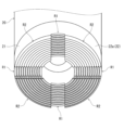
- a jig 90 shown in FIGS. 6(a) to 6(d) is used.
- the jig 90 is shaped like a rectangular plate as a whole.
- the jig 90 has a concave portion 91 corresponding to the non-overlapping region R2 on its one surface.
- Four concave portions 91 are provided in the present embodiment, each of which is fan-shaped.
- a slit 92 corresponding to the overlapping region R1 is formed between adjacent recesses 91 .
- a pressing portion 93 for pressing the negative electrode current collecting plate 40 is provided in the central portion of the jig 90 .
- the negative electrode 21 and the negative electrode current collector 40 are electrically connected with the negative electrode current collector 40 sandwiched between the jig 90 and the wound body 20. connect to.
- a bent portion bent surface 22c
- FIG. 7A shows the laser beam L used for laser welding.
- the wound body 20 and the negative electrode current collector plate 40 are accommodated in the case 30, and the negative electrode current collector 22 is brought into contact with the bottom of the case 30 in at least a part of the non-overlapping region of the negative electrode 21 to form the contact portion 22b. to form
- the negative electrode current collector plate 40 and the case 30 are electrically connected.
- This electrical connection may be made, for example, by laser welding.
- the method for manufacturing a power storage device of this embodiment includes a fourth step and a fifth step.
- the fifth step is executed after the fourth step, but the execution order of both steps is not limited to this.
- the negative electrode current collector 22 is pressed down to shift the non-overlapping region R2 to the overlapping region R1 before the first to third steps.
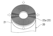
- the fourth step may be performed by pressing a roller (not shown) against the negative electrode current collector exposed portion 22a and rolling the roller in the direction of the arrow in FIG. 8A.
- the negative electrode current collector 22 is pressed shallower than in the fourth step in the non-overlapping region R2 of the negative electrode 21 to form a non-overlapping region.
- a surface (bent surface 22c) bent with respect to the axial direction is formed in the overlapping region R2.
- the fifth step may be performed by pressing a roller (not shown) against the negative electrode current collector exposed portion 22a and rolling the roller in the direction of the arrow in FIG. 8B.
- the present disclosure can be used for a power storage device and a method for manufacturing the power storage device.
Landscapes
- Engineering & Computer Science (AREA)
- Chemical & Material Sciences (AREA)
- Chemical Kinetics & Catalysis (AREA)
- Electrochemistry (AREA)
- General Chemical & Material Sciences (AREA)
- Power Engineering (AREA)
- Manufacturing & Machinery (AREA)
- Microelectronics & Electronic Packaging (AREA)
- Secondary Cells (AREA)
- Connection Of Batteries Or Terminals (AREA)
- Electric Double-Layer Capacitors Or The Like (AREA)
Priority Applications (4)
| Application Number | Priority Date | Filing Date | Title |
|---|---|---|---|
| US18/682,092 US20250023204A1 (en) | 2021-09-30 | 2022-09-28 | Power storage device and method for manufacturing power storage device |
| EP22876363.7A EP4411974A4 (en) | 2021-09-30 | 2022-09-28 | Power storage device and method for manufacturing power storage device |
| CN202280054020.XA CN117795762A (zh) | 2021-09-30 | 2022-09-28 | 蓄电装置和蓄电装置的制造方法 |
| JP2023551614A JP7843462B2 (ja) | 2021-09-30 | 2022-09-28 | 蓄電装置および蓄電装置の製造方法 |
Applications Claiming Priority (2)
| Application Number | Priority Date | Filing Date | Title |
|---|---|---|---|
| JP2021-161249 | 2021-09-30 | ||
| JP2021161249 | 2021-09-30 |
Publications (1)
| Publication Number | Publication Date |
|---|---|
| WO2023054497A1 true WO2023054497A1 (ja) | 2023-04-06 |
Family
ID=85780728
Family Applications (1)
| Application Number | Title | Priority Date | Filing Date |
|---|---|---|---|
| PCT/JP2022/036230 Ceased WO2023054497A1 (ja) | 2021-09-30 | 2022-09-28 | 蓄電装置および蓄電装置の製造方法 |
Country Status (5)
| Country | Link |
|---|---|
| US (1) | US20250023204A1 (https=) |
| EP (1) | EP4411974A4 (https=) |
| JP (1) | JP7843462B2 (https=) |
| CN (1) | CN117795762A (https=) |
| WO (1) | WO2023054497A1 (https=) |
Citations (3)
| Publication number | Priority date | Publication date | Assignee | Title |
|---|---|---|---|---|
| JP2000260418A (ja) * | 1999-03-12 | 2000-09-22 | Furukawa Battery Co Ltd:The | 円筒型蓄電池用集電体並びに円筒型蓄電池 |
| JP2001102031A (ja) * | 1999-09-30 | 2001-04-13 | Sanyo Electric Co Ltd | 電気エネルギー蓄積デバイス及びその製造方法 |
| JP2010257851A (ja) * | 2009-04-27 | 2010-11-11 | Toyota Motor Corp | 電池の製造方法 |
Family Cites Families (3)
| Publication number | Priority date | Publication date | Assignee | Title |
|---|---|---|---|---|
| JP4446205B2 (ja) * | 2008-04-14 | 2010-04-07 | トヨタ自動車株式会社 | 電池およびその製造方法 |
| WO2019004039A1 (ja) * | 2017-06-28 | 2019-01-03 | 三洋電機株式会社 | 電池及びその製造方法 |
| CN114207918B (zh) * | 2019-08-08 | 2024-05-10 | 株式会社村田制作所 | 二次电池、电池包、电子设备、电动工具及电动车辆 |
-
2022
- 2022-09-28 US US18/682,092 patent/US20250023204A1/en active Pending
- 2022-09-28 WO PCT/JP2022/036230 patent/WO2023054497A1/ja not_active Ceased
- 2022-09-28 JP JP2023551614A patent/JP7843462B2/ja active Active
- 2022-09-28 EP EP22876363.7A patent/EP4411974A4/en active Pending
- 2022-09-28 CN CN202280054020.XA patent/CN117795762A/zh active Pending
Patent Citations (3)
| Publication number | Priority date | Publication date | Assignee | Title |
|---|---|---|---|---|
| JP2000260418A (ja) * | 1999-03-12 | 2000-09-22 | Furukawa Battery Co Ltd:The | 円筒型蓄電池用集電体並びに円筒型蓄電池 |
| JP2001102031A (ja) * | 1999-09-30 | 2001-04-13 | Sanyo Electric Co Ltd | 電気エネルギー蓄積デバイス及びその製造方法 |
| JP2010257851A (ja) * | 2009-04-27 | 2010-11-11 | Toyota Motor Corp | 電池の製造方法 |
Non-Patent Citations (1)
| Title |
|---|
| See also references of EP4411974A4 * |
Also Published As
| Publication number | Publication date |
|---|---|
| EP4411974A1 (en) | 2024-08-07 |
| US20250023204A1 (en) | 2025-01-16 |
| EP4411974A4 (en) | 2025-05-14 |
| JPWO2023054497A1 (https=) | 2023-04-06 |
| CN117795762A (zh) | 2024-03-29 |
| JP7843462B2 (ja) | 2026-04-10 |
Similar Documents
| Publication | Publication Date | Title |
|---|---|---|
| JP6550848B2 (ja) | 角形二次電池 | |
| WO2023286687A1 (ja) | 集電板およびこれを用いた蓄電装置 | |
| KR20040094792A (ko) | 이차 전지 | |
| JP7167427B2 (ja) | 二次電池 | |
| US20220271399A1 (en) | Battery | |
| US10608233B2 (en) | Method of manufacturing secondary battery | |
| CN111902968A (zh) | 电池以及其制造方法 | |
| JP7734325B2 (ja) | 蓄電装置 | |
| WO2021039267A1 (ja) | 角形二次電池及びその製造方法 | |
| JPWO2019116914A1 (ja) | 蓄電素子 | |
| WO2023054497A1 (ja) | 蓄電装置および蓄電装置の製造方法 | |
| JP7702674B2 (ja) | 蓄電装置 | |
| CN119009149A (zh) | 蓄电单元 | |
| KR102733272B1 (ko) | 이차전지 | |
| WO2023127565A1 (ja) | 集電板および蓄電装置 | |
| WO2022249780A1 (ja) | 接合方法 | |
| CN115635180A (zh) | 焊头、端子部件以及二次电池 | |
| WO2021187349A1 (ja) | 密閉電池 | |
| EP4318515A1 (en) | Power storage device | |
| JP7702673B2 (ja) | 蓄電装置 | |
| US20250096431A1 (en) | Power storage cell | |
| US20250096434A1 (en) | Power storage cell | |
| US20250105302A1 (en) | Power storage cell | |
| WO2025205532A1 (ja) | 円筒形電池の製造方法、及び円筒形電池 | |
| WO2025115651A1 (ja) | 円筒形電池 |
Legal Events
| Date | Code | Title | Description |
|---|---|---|---|
| 121 | Ep: the epo has been informed by wipo that ep was designated in this application |
Ref document number: 22876363 Country of ref document: EP Kind code of ref document: A1 |
|
| WWE | Wipo information: entry into national phase |
Ref document number: 2023551614 Country of ref document: JP |
|
| WWE | Wipo information: entry into national phase |
Ref document number: 202280054020.X Country of ref document: CN |
|
| WWE | Wipo information: entry into national phase |
Ref document number: 18682092 Country of ref document: US Ref document number: 202447008218 Country of ref document: IN |
|
| NENP | Non-entry into the national phase |
Ref country code: DE |
|
| ENP | Entry into the national phase |
Ref document number: 2022876363 Country of ref document: EP Effective date: 20240430 |