WO2023054497A1 - Power storage device and method for manufacturing power storage device - Google Patents
Power storage device and method for manufacturing power storage device Download PDFInfo
- Publication number
- WO2023054497A1 WO2023054497A1 PCT/JP2022/036230 JP2022036230W WO2023054497A1 WO 2023054497 A1 WO2023054497 A1 WO 2023054497A1 JP 2022036230 W JP2022036230 W JP 2022036230W WO 2023054497 A1 WO2023054497 A1 WO 2023054497A1
- Authority
- WO
- WIPO (PCT)
- Prior art keywords
- current collector
- case
- electrode
- overlapping region
- storage device
- Prior art date
Links
- 238000003860 storage Methods 0.000 title claims abstract description 81
- 238000004519 manufacturing process Methods 0.000 title claims description 32
- 238000000034 method Methods 0.000 title claims description 27
- 239000011149 active material Substances 0.000 claims description 10
- 238000003825 pressing Methods 0.000 claims description 8
- 238000005452 bending Methods 0.000 claims description 5
- 238000003466 welding Methods 0.000 description 14
- 238000007789 sealing Methods 0.000 description 11
- 239000007773 negative electrode material Substances 0.000 description 10
- 239000007774 positive electrode material Substances 0.000 description 10
- 239000007769 metal material Substances 0.000 description 7
- HBBGRARXTFLTSG-UHFFFAOYSA-N Lithium ion Chemical group [Li+] HBBGRARXTFLTSG-UHFFFAOYSA-N 0.000 description 6
- 238000010586 diagram Methods 0.000 description 6
- 229910001416 lithium ion Inorganic materials 0.000 description 6
- 229910052751 metal Inorganic materials 0.000 description 6
- 239000002184 metal Substances 0.000 description 6
- PXHVJJICTQNCMI-UHFFFAOYSA-N Nickel Chemical compound [Ni] PXHVJJICTQNCMI-UHFFFAOYSA-N 0.000 description 4
- 239000011230 binding agent Substances 0.000 description 4
- 239000006258 conductive agent Substances 0.000 description 4
- 239000000463 material Substances 0.000 description 4
- 238000005096 rolling process Methods 0.000 description 4
- 238000005219 brazing Methods 0.000 description 3
- 239000003990 capacitor Substances 0.000 description 3
- 239000011248 coating agent Substances 0.000 description 3
- 238000000576 coating method Methods 0.000 description 3
- 238000004804 winding Methods 0.000 description 3
- 238000004026 adhesive bonding Methods 0.000 description 2
- 229910052782 aluminium Inorganic materials 0.000 description 2
- XAGFODPZIPBFFR-UHFFFAOYSA-N aluminium Chemical compound [Al] XAGFODPZIPBFFR-UHFFFAOYSA-N 0.000 description 2
- 238000007599 discharging Methods 0.000 description 2
- 238000001035 drying Methods 0.000 description 2
- 239000011888 foil Substances 0.000 description 2
- 239000000203 mixture Substances 0.000 description 2
- 229910052759 nickel Inorganic materials 0.000 description 2
- 229920000447 polyanionic polymer Polymers 0.000 description 2
- 239000002002 slurry Substances 0.000 description 2
- 229910000838 Al alloy Inorganic materials 0.000 description 1
- RYGMFSIKBFXOCR-UHFFFAOYSA-N Copper Chemical compound [Cu] RYGMFSIKBFXOCR-UHFFFAOYSA-N 0.000 description 1
- 229910000881 Cu alloy Inorganic materials 0.000 description 1
- WHXSMMKQMYFTQS-UHFFFAOYSA-N Lithium Chemical compound [Li] WHXSMMKQMYFTQS-UHFFFAOYSA-N 0.000 description 1
- RTAQQCXQSZGOHL-UHFFFAOYSA-N Titanium Chemical compound [Ti] RTAQQCXQSZGOHL-UHFFFAOYSA-N 0.000 description 1
- 229910045601 alloy Inorganic materials 0.000 description 1
- 239000000956 alloy Substances 0.000 description 1
- 239000003575 carbonaceous material Substances 0.000 description 1
- 229910010293 ceramic material Inorganic materials 0.000 description 1
- 239000010949 copper Substances 0.000 description 1
- 229910052802 copper Inorganic materials 0.000 description 1
- 230000002950 deficient Effects 0.000 description 1
- 230000000694 effects Effects 0.000 description 1
- 230000017525 heat dissipation Effects 0.000 description 1
- 229910052744 lithium Inorganic materials 0.000 description 1
- 150000002736 metal compounds Chemical class 0.000 description 1
- 239000012982 microporous membrane Substances 0.000 description 1
- 239000004745 nonwoven fabric Substances 0.000 description 1
- 229920000098 polyolefin Polymers 0.000 description 1
- 230000005855 radiation Effects 0.000 description 1
- 239000011347 resin Substances 0.000 description 1
- 229920005989 resin Polymers 0.000 description 1
- 239000010935 stainless steel Substances 0.000 description 1
- 229910001220 stainless steel Inorganic materials 0.000 description 1
- 239000010936 titanium Substances 0.000 description 1
- 229910052719 titanium Inorganic materials 0.000 description 1
- 229910052723 transition metal Inorganic materials 0.000 description 1
- 229910021561 transition metal fluoride Inorganic materials 0.000 description 1
- 229910000314 transition metal oxide Inorganic materials 0.000 description 1
- -1 transition metal sulfides Chemical class 0.000 description 1
- 239000002759 woven fabric Substances 0.000 description 1
Images


Classifications
-
- H—ELECTRICITY
- H01—ELECTRIC ELEMENTS
- H01G—CAPACITORS; CAPACITORS, RECTIFIERS, DETECTORS, SWITCHING DEVICES OR LIGHT-SENSITIVE DEVICES, OF THE ELECTROLYTIC TYPE
- H01G11/00—Hybrid capacitors, i.e. capacitors having different positive and negative electrodes; Electric double-layer [EDL] capacitors; Processes for the manufacture thereof or of parts thereof
- H01G11/66—Current collectors
- H01G11/70—Current collectors characterised by their structure
-
- H—ELECTRICITY
- H01—ELECTRIC ELEMENTS
- H01G—CAPACITORS; CAPACITORS, RECTIFIERS, DETECTORS, SWITCHING DEVICES OR LIGHT-SENSITIVE DEVICES, OF THE ELECTROLYTIC TYPE
- H01G11/00—Hybrid capacitors, i.e. capacitors having different positive and negative electrodes; Electric double-layer [EDL] capacitors; Processes for the manufacture thereof or of parts thereof
- H01G11/74—Terminals, e.g. extensions of current collectors
-
- H—ELECTRICITY
- H01—ELECTRIC ELEMENTS
- H01G—CAPACITORS; CAPACITORS, RECTIFIERS, DETECTORS, SWITCHING DEVICES OR LIGHT-SENSITIVE DEVICES, OF THE ELECTROLYTIC TYPE
- H01G11/00—Hybrid capacitors, i.e. capacitors having different positive and negative electrodes; Electric double-layer [EDL] capacitors; Processes for the manufacture thereof or of parts thereof
- H01G11/78—Cases; Housings; Encapsulations; Mountings
- H01G11/82—Fixing or assembling a capacitive element in a housing, e.g. mounting electrodes, current collectors or terminals in containers or encapsulations
-
- H—ELECTRICITY
- H01—ELECTRIC ELEMENTS
- H01G—CAPACITORS; CAPACITORS, RECTIFIERS, DETECTORS, SWITCHING DEVICES OR LIGHT-SENSITIVE DEVICES, OF THE ELECTROLYTIC TYPE
- H01G11/00—Hybrid capacitors, i.e. capacitors having different positive and negative electrodes; Electric double-layer [EDL] capacitors; Processes for the manufacture thereof or of parts thereof
- H01G11/84—Processes for the manufacture of hybrid or EDL capacitors, or components thereof
-
- H—ELECTRICITY
- H01—ELECTRIC ELEMENTS
- H01M—PROCESSES OR MEANS, e.g. BATTERIES, FOR THE DIRECT CONVERSION OF CHEMICAL ENERGY INTO ELECTRICAL ENERGY
- H01M50/00—Constructional details or processes of manufacture of the non-active parts of electrochemical cells other than fuel cells, e.g. hybrid cells
- H01M50/10—Primary casings, jackets or wrappings of a single cell or a single battery
- H01M50/102—Primary casings, jackets or wrappings of a single cell or a single battery characterised by their shape or physical structure
- H01M50/107—Primary casings, jackets or wrappings of a single cell or a single battery characterised by their shape or physical structure having curved cross-section, e.g. round or elliptic
-
- H—ELECTRICITY
- H01—ELECTRIC ELEMENTS
- H01M—PROCESSES OR MEANS, e.g. BATTERIES, FOR THE DIRECT CONVERSION OF CHEMICAL ENERGY INTO ELECTRICAL ENERGY
- H01M50/00—Constructional details or processes of manufacture of the non-active parts of electrochemical cells other than fuel cells, e.g. hybrid cells
- H01M50/50—Current conducting connections for cells or batteries
- H01M50/531—Electrode connections inside a battery casing
- H01M50/533—Electrode connections inside a battery casing characterised by the shape of the leads or tabs
-
- H—ELECTRICITY
- H01—ELECTRIC ELEMENTS
- H01M—PROCESSES OR MEANS, e.g. BATTERIES, FOR THE DIRECT CONVERSION OF CHEMICAL ENERGY INTO ELECTRICAL ENERGY
- H01M50/00—Constructional details or processes of manufacture of the non-active parts of electrochemical cells other than fuel cells, e.g. hybrid cells
- H01M50/50—Current conducting connections for cells or batteries
- H01M50/531—Electrode connections inside a battery casing
- H01M50/538—Connection of several leads or tabs of wound or folded electrode stacks
-
- H—ELECTRICITY
- H01—ELECTRIC ELEMENTS
- H01M—PROCESSES OR MEANS, e.g. BATTERIES, FOR THE DIRECT CONVERSION OF CHEMICAL ENERGY INTO ELECTRICAL ENERGY
- H01M50/00—Constructional details or processes of manufacture of the non-active parts of electrochemical cells other than fuel cells, e.g. hybrid cells
- H01M50/50—Current conducting connections for cells or batteries
- H01M50/543—Terminals
- H01M50/545—Terminals formed by the casing of the cells
-
- H—ELECTRICITY
- H01—ELECTRIC ELEMENTS
- H01M—PROCESSES OR MEANS, e.g. BATTERIES, FOR THE DIRECT CONVERSION OF CHEMICAL ENERGY INTO ELECTRICAL ENERGY
- H01M50/00—Constructional details or processes of manufacture of the non-active parts of electrochemical cells other than fuel cells, e.g. hybrid cells
- H01M50/50—Current conducting connections for cells or batteries
- H01M50/543—Terminals
- H01M50/552—Terminals characterised by their shape
- H01M50/559—Terminals adapted for cells having curved cross-section, e.g. round, elliptic or button cells
- H01M50/56—Cup shaped terminals
Abstract
A power storage device according to the present invention includes: a first electrode having a first current collector, a second electrode having a second current collector, and a separator interposed between the first electrode and the second electrode. The first electrode, the second electrode, and the separator constitute a columnar wound body. The power storage device further includes a cylindrical bottomed case for accommodating the wound body, and a current collecting plate electrically connected to the first electrode and the case. The first electrode has an overlapping region that overlaps the current collecting plate when viewed in the axial direction of the case, and a non-overlapping region that does not overlap the current collecting plate when viewed in the axial direction. The first electrode and the current collecting plate are electrically connected to each other in the overlapping region. The first current collector includes a contact portion that is provided in at least a part of the non-overlapping region and that is in contact with the bottom of the case.
Description
本開示は、蓄電装置および蓄電装置の製造方法に関する。
The present disclosure relates to a power storage device and a method for manufacturing the power storage device.
従来、一端に集電体が露出した電極体と、電極体を収容する有底筒状のケースと、電極体とケースの底部との間に設けられた集電板とを備えた蓄電装置が知られている(例えば、特許文献1)。特許文献1の蓄電装置では、集電板が、露出した集電体とケースの底部とに機械的かつ電気的に接続されている。
Conventionally, there is a power storage device that includes an electrode body with an exposed current collector at one end, a cylindrical case with a bottom that houses the electrode body, and a current collector plate provided between the electrode body and the bottom of the case. known (for example, Patent Document 1). In the power storage device of Patent Document 1, the collector plate is mechanically and electrically connected to the exposed collector and the bottom of the case.
ところで、蓄電装置の信頼性のさらなる改善が望まれている。このような状況において、本開示は、蓄電装置の信頼性を改善することを目的の1つとする。
By the way, further improvement in the reliability of power storage devices is desired. Under such circumstances, one object of the present disclosure is to improve the reliability of the power storage device.
本開示に係る一局面は、蓄電装置に関する。当該蓄電装置は、帯状の第1集電体、および前記第1集電体に担持された第1活物質層を有する第1電極と、帯状の第2集電体、および前記第2集電体に担持された第2活物質層を有する第2電極と、前記第1電極と前記第2電極との間に介在するセパレータと、を備え、前記第1電極、前記第2電極、および前記セパレータは、柱状の巻回体を構成しており、前記巻回体を収容する有底筒状のケースと、前記第1電極と前記ケースの底部との間に設けられ、両者に電気的に接続される集電板と、をさらに備え、前記第1電極は、前記ケースの軸方向から見て前記集電板と重なる重複領域と、前記軸方向から見て前記集電板と重ならない非重複領域とを有し、前記第1電極と前記集電板とは、前記重複領域において互いに電気的に接続されており、前記第1電極の前記第1集電体は、前記非重複領域の少なくとも一部に設けられ、前記ケースの底部に接触する接触部を有する。
One aspect of the present disclosure relates to a power storage device. The power storage device includes a strip-shaped first current collector, a first electrode having a first active material layer supported on the first current collector, a strip-shaped second current collector, and the second current collector. a second electrode having a second active material layer supported on a body; and a separator interposed between the first electrode and the second electrode, wherein the first electrode, the second electrode, and the The separator constitutes a columnar wound body, and is provided between a cylindrical case with a bottom that accommodates the wound body, and the first electrode and the bottom of the case. and a current collector plate to be connected, wherein the first electrode has an overlapping region overlapping with the current collector plate when viewed from the axial direction of the case, and a non-overlapping region not overlapping with the current collector plate when viewed from the axial direction of the case. an overlap region, wherein the first electrode and the current collector are electrically connected to each other in the overlap region, and the first current collector of the first electrode is located in the non-overlap region It has a contact portion which is provided on at least a part thereof and contacts the bottom portion of the case.
本開示に係る別の一局面は、蓄電装置の製造方法に関する。当該製造方法は、上述の蓄電装置の製造方法であって、前記重複領域において、前記巻回体の前記第1電極と前記集電板とを電気的に接続する第1工程と、前記巻回体および前記集電板を前記ケースに収容し、前記非重複領域の少なくとも一部において前記第1集電体を前記ケースの底部に接触させて前記接触部を形成する第2工程と、前記集電板と前記ケースとを電気的に接続する第3工程と、を備える。
Another aspect of the present disclosure relates to a method for manufacturing a power storage device. The manufacturing method is a method for manufacturing the power storage device described above, and includes a first step of electrically connecting the first electrode of the wound body and the current collector plate in the overlap region; a second step of housing the body and the current collector in the case, and bringing the first current collector into contact with the bottom of the case in at least part of the non-overlapping region to form the contact portion; and a third step of electrically connecting the electric plate and the case.
本開示によれば、蓄電装置の信頼性を改善することができる。
According to the present disclosure, it is possible to improve the reliability of the power storage device.
本開示に係る蓄電装置および蓄電装置の製造方法の実施形態について例を挙げて以下に説明する。しかしながら、本開示は以下に説明する例に限定されない。以下の説明では、具体的な数値や材料を例示する場合があるが、本開示の効果が得られる限り、他の数値や材料を適用してもよい。
Embodiments of the power storage device and the method for manufacturing the power storage device according to the present disclosure will be described below with examples. However, the disclosure is not limited to the examples described below. In the following description, specific numerical values and materials may be exemplified, but other numerical values and materials may be applied as long as the effects of the present disclosure can be obtained.
(蓄電装置)
本開示に係る蓄電装置は、帯状の第1電極と、帯状の第2電極と、両者の間に介在するセパレータとを備える。第1電極、第2電極、およびセパレータは、柱状の巻回体を構成している。すなわち、第1電極と第2電極とは、セパレータを介して巻回されている。 (Power storage device)
A power storage device according to the present disclosure includes a strip-shaped first electrode, a strip-shaped second electrode, and a separator interposed therebetween. The first electrode, the second electrode, and the separator constitute a columnar wound body. That is, the first electrode and the second electrode are wound with the separator interposed therebetween.
第1電極は、帯状の第1集電体と、第1集電体に担持された第1活物質層とを有する。第2電極は、帯状の第2集電体と、第2集電体に担持された第2活物質層とを有する。
The first electrode has a strip-shaped first current collector and a first active material layer carried on the first current collector. The second electrode has a strip-shaped second current collector and a second active material layer carried on the second current collector.
蓄電装置は、上記巻回体を収容する有底筒状のケースと、第1電極とケースの底部との間に設けられ、両者に電気的に接続される集電板とをさらに備える。
The power storage device further includes a cylindrical case with a bottom that houses the wound body, and a collector plate that is provided between the first electrode and the bottom of the case and electrically connected to both.
第1電極は、ケースの軸方向(以下、単に軸方向ともいう。)から見て集電板と重なる重複領域と、軸方向から見て集電板と重ならない非重複領域とを有する。重複領域の形状は、集電板の形状に対応している。例えば、集電板が十字形状を有する場合、重複領域も十字形状を有する。非重複領域は、軸方向から見て、第1電極のうち重複領域に含まれない領域である。
The first electrode has an overlapping region that overlaps the current collector plate when viewed from the axial direction of the case (hereinafter also simply referred to as the axial direction) and a non-overlapping region that does not overlap the current collector plate when viewed from the axial direction. The shape of the overlapping region corresponds to the shape of the current collector plate. For example, if the current collector plate has a cross shape, the overlap region also has a cross shape. A non-overlapping region is a region of the first electrode that is not included in the overlapping region when viewed in the axial direction.
第1電極と集電板とは、重複領域において互いに電気的に接続されている。この接続は、種々の態様で実現されてもよい。例えば、第1電極と集電板とは、溶接(例えば、レーザ溶接)により、ろう付けにより、または接着により互いに接続されてもよい。第1電極と集電板とは、重複領域において互いに電気的かつ機械的に接続されていてもよい。
The first electrode and the current collector plate are electrically connected to each other in the overlapping region. This connection may be implemented in various ways. For example, the first electrode and the current collector plate may be connected to each other by welding (eg, laser welding), by brazing, or by gluing. The first electrode and the current collector plate may be electrically and mechanically connected to each other in the overlapping region.
第1電極の第1集電体は、非重複領域の少なくとも一部に設けられ、ケースの底部に接触する接触部を有する。つまり、第1集電体は、重複領域では集電板を介してケースの底部に接続される一方、非重複領域では接触部において直接的にケースの底部に接触する。このため、充放電時に発生する熱を第1電極から放熱する経路として、従来から存在する集電板およびケースを経由する経路に加えて、接触部およびケースを経由する経路が形成される。したがって、蓄電装置の放熱特性を改善でき、蓄電装置の信頼性を高めることができる。さらに、接触部とケースの底部との間に充放電に利用可能な電流経路が形成されるので、蓄電装置の低抵抗化を図ることができる。なお、重複領域および非重複領域は、巻回体において蓄電装置の封口板側の端部に形成されていてもよく、接触部が封口板や、集電板と封口板とを電気的に接続する導電部材に当接していてもよい。
The first current collector of the first electrode has a contact portion provided in at least part of the non-overlapping region and in contact with the bottom of the case. That is, the first current collector is connected to the bottom of the case via the current collector plate in the overlap region, while directly contacting the bottom of the case at the contact portion in the non-overlap region. Therefore, in addition to the existing path through the current collector plate and case, a path through the contact portion and case is formed as a path through which heat generated during charging and discharging is dissipated from the first electrode. Therefore, the heat radiation characteristic of the power storage device can be improved, and the reliability of the power storage device can be enhanced. Furthermore, since a current path that can be used for charging and discharging is formed between the contact portion and the bottom portion of the case, it is possible to reduce the resistance of the power storage device. The overlapping region and the non-overlapping region may be formed at the end of the power storage device on the side of the sealing plate in the wound body, and the contact portion electrically connects the sealing plate or the current collecting plate and the sealing plate. It may be in contact with the conductive member.
第1集電体は、その短手方向(あるいは、幅方向)の一端に第1活物質層が形成されていない第1未塗布部を有してもよい。巻回体では、ケースの軸方向において、第1未塗布部が第2電極から突出した状態で第1電極、第2電極、およびセパレータが巻回されてもよい。重複領域および非重複領域は、巻回された第1未塗布部で構成されていてもよい。
The first current collector may have a first uncoated portion where the first active material layer is not formed at one end in its short direction (or width direction). In the wound body, the first electrode, the second electrode, and the separator may be wound with the first uncoated portion protruding from the second electrode in the axial direction of the case. The overlapping area and the non-overlapping area may be comprised of a rolled first uncoated portion.
接触部は、ケースの径方向に屈曲していると共にケースの底部に面接触していてもよい。この構成によると、接触部とケースの底部との間の伝熱特性が高まり、蓄電装置の放熱特性をより一層改善することができる。さらに、ケースの底部に面接触する接触部により、巻回体の姿勢を安定させることができる。
The contact portion may be bent in the radial direction of the case and may be in surface contact with the bottom of the case. According to this configuration, the heat transfer characteristics between the contact portion and the bottom portion of the case are enhanced, and the heat dissipation characteristics of the power storage device can be further improved. Furthermore, the contact portion that makes surface contact with the bottom portion of the case can stabilize the posture of the wound body.
接触部は、ケースの径方向内側に向かって屈曲していてもよい。例えば、接触部は、第1集電体の端部をケースの径方向内側に屈曲させて形成されていてもよい。これにより、第1電極が破れるのを抑止しつつ、接触部を容易に形成することができる。
The contact portion may be bent radially inward of the case. For example, the contact portion may be formed by bending the end portion of the first current collector radially inward of the case. This makes it possible to easily form the contact portion while suppressing breakage of the first electrode.
集電板は、ケースと接続する接続部と、接続部からケースの径方向に延びて第1電極と接続する少なくとも1つのアーム部と、を有してもよい。また、集電板において、接続部は中心に位置し、アーム部よりもケースの底部に向かって突出していてもよい。このような接続部を用いることにより、ケースの底部に対して、接続部を巻回体側からケースの底部側へ向かって容易に押し当てることができる。そのため、この接続部とケースの底部とをケースの外から溶接して接合する際に、ケースの底部と接続部とが離れていることにより発生する溶接不良を抑制することができる。また、接続部において、ケースの底部と対向する面の裏側の面は窪んでいてもよい。
The current collector plate may have a connection portion connected to the case, and at least one arm portion extending from the connection portion in a radial direction of the case and connected to the first electrode. Moreover, in the current collector plate, the connecting portion may be located in the center and protrude toward the bottom portion of the case rather than the arm portion. By using such a connecting portion, the connecting portion can be easily pressed against the bottom portion of the case from the wound body side toward the bottom portion side of the case. Therefore, when the connecting portion and the bottom portion of the case are welded together from the outside of the case, it is possible to suppress defective welding caused by the distance between the bottom portion of the case and the connecting portion. In addition, in the connecting portion, the back surface of the surface facing the bottom of the case may be recessed.
ケースの軸方向において、非重複領域の第1集電体のうち、集電板と第1電極との接続箇所よりもケースの底部に向かって延びる部分の長さは、集電板と第1電極との接続箇所から集電板とケースの底部との接続箇所までの距離よりも長くてもよい。この構成により、第1集電体の軸方向の先端(接触部)を屈曲させた状体でケースの底部と当接させることが容易に実現できる。
In the axial direction of the case, the length of the portion of the first current collector in the non-overlapping region extending toward the bottom of the case from the connection point between the current collector and the first electrode is equal to the length of the current collector and the first electrode. It may be longer than the distance from the connection point with the electrode to the connection point between the collector plate and the bottom of the case. With this configuration, it is possible to easily achieve contact with the bottom portion of the case by bending the tip (contact portion) of the first current collector in the axial direction.
接触部は、ケースの径方向において巻回体の外側よりも内側に近くてもよい。または、接触部は、ケースの周方向において非重複領域の内側よりも外側に近くてもよい。この構成により、より簡便に非重複領域に接触部を形成できる。また、接触部における集電体を密にすることができる。また、非重複領域における第1集電体の破断を抑制することができ、蓄電装置の信頼性が高まる。
The contact portion may be closer to the inside than the outside of the wound body in the radial direction of the case. Alternatively, the contact portion may be closer to the outside than the inside of the non-overlapping region in the circumferential direction of the case. With this configuration, the contact portion can be formed in the non-overlapping region more easily. In addition, the current collector can be made dense at the contact portion. Moreover, breakage of the first current collector in the non-overlapping region can be suppressed, and the reliability of the power storage device increases.
非重複領域は、ケースの径方向において接触部よりも外側に配置され、接触部よりもケースの底部から遠い領域(非接触領域)を有してもよい。この構成により、より簡便に非重複領域に接触部を形成できる。また、非重複領域で、ケースの径方向において、より内側に接触部を設けることにより、径方向において外側に設けられた接触部より、接触部の周方向寸法が小さくなるので、接触部を構成する集電体に周方向のテンションが抑制され、接触部を構成する集電体が径方向に曲がり(又は反り)にくくより高く接触部を形成しやすい。
The non-overlapping region may have a region (non-contact region) located outside the contact portion in the radial direction of the case and farther from the bottom of the case than the contact portion. With this configuration, the contact portion can be formed in the non-overlapping region more easily. In addition, in the non-overlapping region, the contact portion is provided more inside in the radial direction of the case, so that the circumferential dimension of the contact portion is smaller than that of the contact portion provided on the outer side in the radial direction. The tension in the circumferential direction is suppressed in the current collector, and the current collector constituting the contact portion is less likely to bend (or warp) in the radial direction, making it easier to form the contact portion at a higher height.
第1集電体は、重複領域および非重複領域においてケースの径方向に屈曲していて、重複領域の屈曲部分の方が非重複領域の屈曲部分よりも長くてもよい。この構成では、重複領域での第1集電体の変形代が小さいため、重複領域における剛性を高めることが可能となり、集電板をこの重複領域で接合する際に、集電板を介して重複領域の第1集電体を押したときに当該第1集電体から反力を得やすくなる。そのため、集電板と重複領域の第1集電体との接合が容易になる。
The first current collector may be bent in the radial direction of the case in the overlapping region and the non-overlapping region, and the bent portion of the overlapping region may be longer than the bent portion of the non-overlapping region. In this configuration, since the deformation allowance of the first current collector in the overlapping region is small, it is possible to increase the rigidity in the overlapping region. When the first current collector in the overlapping region is pressed, it becomes easier to obtain a reaction force from the first current collector. Therefore, it becomes easy to join the current collector plate and the first current collector in the overlapping region.
(蓄電装置の製造方法)
本開示に係る蓄電装置の製造方法は、上述の蓄電装置の製造方法であって、第1工程と、第2工程と、第3工程とを備える。 (Method for manufacturing power storage device)
A method for manufacturing a power storage device according to the present disclosure is the above-described method for manufacturing a power storage device, and includes a first step, a second step, and a third step.
第1工程では、第1電極の重複領域において、巻回体の第1電極と集電板とを電気的に接続する。この接続は、種々の態様で実現されてもよい。例えば、第1電極と集電板とは、溶接(例えば、レーザ溶接)により、ろう付けにより、または接着により互いに接続されてもよい。
In the first step, the first electrode of the wound body and the current collecting plate are electrically connected in the overlap region of the first electrode. This connection may be implemented in various ways. For example, the first electrode and the current collector plate may be connected to each other by welding (eg, laser welding), by brazing, or by gluing.
第2工程では、巻回体および集電板をケースに収容し、第1電極の非重複領域の少なくとも一部において第1集電体をケースの底部に接触させて接触部を形成する。接触部は、巻回体および集電板をケースに収容する前に、予め成形されていてもよいし、当該収容時にケースの底部を利用して成形されてもよい。
In the second step, the wound body and the current collector are housed in a case, and the first current collector is brought into contact with the bottom of the case in at least part of the non-overlapping region of the first electrode to form a contact portion. The contact portion may be formed in advance before housing the wound body and the current collector plate in the case, or may be formed using the bottom portion of the case during housing.
第3工程では、集電板とケースとを電気的に接続する。この接続は、種々の態様で実現されてもよい。例えば、集電板とケースとは、レーザ溶接により、超音波溶接により、またはろう付けにより電気的に接続されてもよい。集電板とケースとは、電気的かつ機械的に接続されてもよい。
In the third step, the current collecting plate and the case are electrically connected. This connection may be implemented in various ways. For example, the current collector plate and the case may be electrically connected by laser welding, ultrasonic welding, or brazing. The current collector plate and the case may be electrically and mechanically connected.
第1工程において、非重複領域に対応する凹部を有する治具と巻回体との間に集電板を挟み込んだ状態で、第1電極と集電板とを電気的に接続してもよい。治具は、凹部が形成された面を第1電極に対向させて使用されてもよい。治具と巻回体との間に挟み込まれた集電板により、第1電極の重複領域が集電板の形状にしたがって凹む。一方、第1電極の非重複領域は、治具の凹部に収容されると共に、その端部が当該凹部の底面に当接して屈曲される。これにより、第1電極の非重複領域に、ケースの底部に面接触する接触部に対応する形状が与えられる。
In the first step, the first electrode and the current collector may be electrically connected in a state in which the current collector is sandwiched between a jig having recesses corresponding to the non-overlapping regions and the winding body. . The jig may be used with the surface on which the concave portion is formed facing the first electrode. Due to the current collector sandwiched between the jig and the wound body, the overlapping region of the first electrode is recessed according to the shape of the current collector. On the other hand, the non-overlapping region of the first electrode is accommodated in the concave portion of the jig, and its end portion contacts the bottom surface of the concave portion and is bent. This gives the non-overlapping region of the first electrode a shape corresponding to the contact portion that makes surface contact with the bottom of the case.
蓄電装置の製造方法は、第1~第3工程よりも前に、第1電極の重複領域において、第1集電体を押さえ込んで非重複領域を重複領域よりも突出させる第4工程と、第1~第3工程よりも前に、第1電極の非重複領域において、第4工程よりも浅く第1集電体を押さえ込んで非重複領域に軸方向に対して屈曲した面を形成する第5工程と、をさらに備えてもよい。第4工程では、重複領域を集電板の形状に対応するように押さえ込んでもよい。第5工程は、非重複領域に、ケースの底部に面接触する接触部に対応する形状が与えられる。第4工程および第5工程における第1電極の押さえ込みには、種々の器具(例えば、ローラ)を用い得る。なお、第4工程と第5工程の実行順序は、どちらが先であってもよいし、両工程が同時に実行されてもよい。
A method for manufacturing a power storage device includes, prior to the first to third steps, a fourth step of holding down the first current collector in the overlapping region of the first electrodes to project the non-overlapping region from the overlapping region; A fifth step of pressing down the first current collector shallower than in the fourth step in the non-overlapping region of the first electrode before the first to third steps to form a curved surface in the non-overlapping region with respect to the axial direction. and a step. In the fourth step, the overlapping region may be pressed so as to correspond to the shape of the current collector plate. A fifth step is to give the non-overlapping region a shape corresponding to the contact portion that makes surface contact with the bottom of the case. Various instruments (for example, rollers) can be used for pressing the first electrode in the fourth and fifth steps. As for the execution order of the fourth step and the fifth step, either may be performed first, or both steps may be performed at the same time.
以上のように、本開示によれば、蓄電装置の信頼性を改善することができる。また、本開示によれば、蓄電装置の低抵抗化を図ることが可能である。さらに、本開示によれば、ケース内において、巻回体の姿勢を安定させることができる。
As described above, according to the present disclosure, it is possible to improve the reliability of the power storage device. Further, according to the present disclosure, it is possible to reduce the resistance of the power storage device. Furthermore, according to the present disclosure, the posture of the wound body can be stabilized within the case.
以下では、本開示に係る蓄電装置および蓄電装置の製造方法の一例について、図面を参照して具体的に説明する。以下で説明する一例の蓄電装置および蓄電装置の製造方法の構成要素および工程には、上述した構成要素および工程を適用できる。以下で説明する一例の蓄電装置および蓄電装置の製造方法の構成要素および工程は、上述した記載に基づいて変更できる。また、以下で説明する事項を、上記の実施形態に適用してもよい。以下で説明する一例の蓄電装置および蓄電装置の製造方法の構成要素および工程のうち、本開示に係る蓄電装置および蓄電装置の製造方法に必須ではない構成要素および工程は省略してもよい。なお、以下で示す図は模式的なものであり、実際の部材の形状や数を正確に反映するものではない。
An example of a power storage device and a method for manufacturing the power storage device according to the present disclosure will be specifically described below with reference to the drawings. The components and steps described above can be applied to the components and steps of the example of the power storage device and the method for manufacturing the power storage device described below. The components and steps of an example power storage device and a method of manufacturing the power storage device described below can be modified based on the above description. Also, the matters described below may be applied to the above embodiments. Among the components and steps of the example of the power storage device and the method for manufacturing the power storage device described below, components and steps that are not essential to the power storage device and the method for manufacturing the power storage device according to the present disclosure may be omitted. It should be noted that the drawings shown below are schematic and do not accurately reflect the actual shape and number of members.
《実施形態1》
本開示の実施形態1について説明する。本実施形態の蓄電装置10は、リチウムイオン二次電池である。しかしながら、本開示の蓄電装置10は、これに限られるものではない。例えば、蓄電装置10は、リチウムイオンキャパシタ、電気二重層コンデンサ、リチウムイオン二次電池とリチウムイオンキャパシタとの中間的な蓄電装置、またはその他の電気化学デバイスであってもよい。 <<Embodiment 1>>
A first embodiment of the present disclosure will be described. Thepower storage device 10 of this embodiment is a lithium ion secondary battery. However, the power storage device 10 of the present disclosure is not limited to this. For example, the power storage device 10 may be a lithium ion capacitor, an electric double layer capacitor, an intermediate power storage device between a lithium ion secondary battery and a lithium ion capacitor, or other electrochemical devices.
本開示の実施形態1について説明する。本実施形態の蓄電装置10は、リチウムイオン二次電池である。しかしながら、本開示の蓄電装置10は、これに限られるものではない。例えば、蓄電装置10は、リチウムイオンキャパシタ、電気二重層コンデンサ、リチウムイオン二次電池とリチウムイオンキャパシタとの中間的な蓄電装置、またはその他の電気化学デバイスであってもよい。 <<Embodiment 1>>
A first embodiment of the present disclosure will be described. The
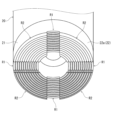
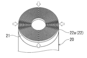
蓄電装置10は、図1~図5に示すように、帯状の負極21と、帯状の正極23と、負極21と正極23との間に介在するセパレータ25とを備える。負極21、正極23、およびセパレータ25は、柱状の巻回体20を構成している。すなわち、負極21と正極23とは、セパレータ25を介して巻回されている。なお、巻回体20において、負極21と正極23とは、後述する正極集電体露出部24aと負極集電体露出部22aとが互いに反対方向に突出するように、軸方向にずれて対向している。
The power storage device 10 includes a strip-shaped negative electrode 21, a strip-shaped positive electrode 23, and a separator 25 interposed between the negative electrode 21 and the positive electrode 23, as shown in FIGS. The negative electrode 21 , the positive electrode 23 , and the separator 25 constitute a columnar wound body 20 . That is, the negative electrode 21 and the positive electrode 23 are wound with the separator 25 interposed therebetween. In the wound body 20, the negative electrode 21 and the positive electrode 23 are offset in the axial direction and face each other such that a positive electrode current collector exposed portion 24a and a negative electrode current collector exposed portion 22a, which will be described later, protrude in opposite directions. are doing.
負極21は、帯状の負極集電体22と、これに担持された負極活物質層(図示せず)とを有する。負極活物質層は、負極集電体22の両面に形成されている。負極集電体22の長手方向に沿う一方の端部には、負極活物質層を有さない負極集電体露出部22aが形成されている。負極21は、第1電極の一例である。負極集電体22は、第1集電体の一例である。負極活物質層は、第1活物質層の一例である。負極集電体露出部22aは、第1未塗布部の一例である。
The negative electrode 21 has a strip-shaped negative electrode current collector 22 and a negative electrode active material layer (not shown) carried thereon. The negative electrode active material layer is formed on both sides of the negative electrode current collector 22 . At one end along the longitudinal direction of the negative electrode current collector 22, a negative electrode current collector exposed portion 22a having no negative electrode active material layer is formed. The negative electrode 21 is an example of a first electrode. The negative electrode current collector 22 is an example of a first current collector. The negative electrode active material layer is an example of the first active material layer. The negative electrode current collector exposed portion 22a is an example of a first uncoated portion.
負極集電体22には、シート状の金属材料が用いられる。シート状の金属材料は、金属箔、金属多孔体などであればよい。金属材料としては、銅、銅合金、ニッケル、ステンレス鋼などを用い得る。負極集電体22の厚さは、例えば、10μm以上、100μm以下である。
A sheet-shaped metal material is used for the negative electrode current collector 22 . The sheet-shaped metal material may be a metal foil, a metal porous body, or the like. As metal materials, copper, copper alloys, nickel, stainless steel, and the like can be used. The thickness of the negative electrode current collector 22 is, for example, 10 μm or more and 100 μm or less.
負極活物質層は、例えば、負極活物質と導電剤と結着剤とを含む。負極活物質層は、例えば、負極集電体22の両面に負極活物質と導電剤と結着剤とを含む負極合材スラリーを塗布し、塗膜を乾燥させた後、圧延することにより得られる。負極活物質は、リチウムイオンを吸蔵および放出する材料である。負極活物質としては、炭素材料、金属化合物、合金、セラミックス材料などが挙げられる。
The negative electrode active material layer contains, for example, a negative electrode active material, a conductive agent, and a binder. The negative electrode active material layer is obtained, for example, by applying a negative electrode mixture slurry containing a negative electrode active material, a conductive agent, and a binder to both surfaces of the negative electrode current collector 22, drying the coating film, and then rolling. be done. A negative electrode active material is a material that absorbs and releases lithium ions. Examples of negative electrode active materials include carbon materials, metal compounds, alloys, and ceramic materials.
正極23は、帯状の正極集電体24と、これに担持された正極活物質層(図示せず)とを有する。正極活物質層は、正極集電体24の両面に形成されている。正極集電体24の長手方向に沿う一方の端部には、正極活物質層を有さない正極集電体露出部24aが形成されている。正極23は、第2電極の一例である。正極集電体24は、第2集電体の一例である。正極活物質層は、第2活物質層の一例である。
The positive electrode 23 has a strip-shaped positive electrode current collector 24 and a positive electrode active material layer (not shown) carried thereon. The positive electrode active material layers are formed on both sides of the positive electrode current collector 24 . At one end along the longitudinal direction of the positive electrode current collector 24, a positive electrode current collector exposed portion 24a having no positive electrode active material layer is formed. The positive electrode 23 is an example of a second electrode. The positive electrode current collector 24 is an example of a second current collector. The positive electrode active material layer is an example of the second active material layer.
正極集電体24には、シート状の金属材料が用いられる。シート状の金属材料は、金属箔、金属多孔体などであればよい。金属材料としては、アルミニウム、アルミニウム合金、ニッケル、チタンなどを用い得る。正極集電体24の厚さは、例えば、10μm以上、100μm以下である。
A sheet-shaped metal material is used for the positive electrode current collector 24 . The sheet-shaped metal material may be a metal foil, a metal porous body, or the like. Aluminum, an aluminum alloy, nickel, titanium, etc. can be used as the metal material. The thickness of the positive electrode current collector 24 is, for example, 10 μm or more and 100 μm or less.
正極活物質層は、例えば、正極活物質と導電剤と結着剤とを含む。正極活物質層は、例えば、正極集電体24の両面に正極活物質と導電剤と結着剤とを含む正極合材スラリーを塗布し、塗膜を乾燥させた後、圧延することにより得られる。正極活物質は、リチウムイオンを吸蔵および放出する材料である。正極活物質としては、例えば、リチウム含有遷移金属酸化物、遷移金属フッ化物、ポリアニオン、フッ素化ポリアニオン、遷移金属硫化物などが挙げられる。
The positive electrode active material layer contains, for example, a positive electrode active material, a conductive agent, and a binder. The positive electrode active material layer is obtained, for example, by coating both surfaces of the positive electrode current collector 24 with a positive electrode mixture slurry containing a positive electrode active material, a conductive agent, and a binder, drying the coating film, and then rolling. be done. A positive electrode active material is a material that absorbs and releases lithium ions. Examples of positive electrode active materials include lithium-containing transition metal oxides, transition metal fluorides, polyanions, fluorinated polyanions, and transition metal sulfides.
セパレータ25としては、帯状であり、例えば、ポリオレフィンなどの樹脂製の微多孔膜、織布、不織布などを用い得る。セパレータ25の厚さは、例えば、10μm以上、300μm以下であり、好ましくは、10μm以上、40μm以下である。
The separator 25 is belt-shaped, and may be made of, for example, a microporous membrane made of resin such as polyolefin, woven fabric, or non-woven fabric. The thickness of the separator 25 is, for example, 10 μm or more and 300 μm or less, preferably 10 μm or more and 40 μm or less.
蓄電装置10は、上記巻回体20を収容する有底筒状のケース30と、負極集電板40および正極集電板50と、ケース30の開口を封止する封口板60とをさらに備える。
Power storage device 10 further includes bottomed cylindrical case 30 that accommodates wound body 20 , negative electrode current collector plate 40 and positive electrode current collector plate 50 , and sealing plate 60 that seals the opening of case 30 . .
ケース30は、金属材料(例えば、アルミニウム)で構成される。ケース30は、有底円筒状であってもよいが、これに限定されるものではない。ケース30は、蓄電装置10の負極端子として機能する。
The case 30 is made of a metal material (eg, aluminum). The case 30 may be cylindrical with a bottom, but is not limited to this. Case 30 functions as a negative terminal of power storage device 10 .
負極集電板40は、負極21(あるいは、巻回体20)とケース30の底部との間に設けられる。負極集電板40は、負極集電体露出部22aおよびケース30の底部に電気的に接続される。負極集電体露出部22aと負極集電板40との間の電気的接続は、例えば、レーザ溶接によりなされてもよい。ケース30の底部と負極集電板40との間の電気的接続は、例えば、超音波溶接によりなされてもよい。負極集電板40は、集電板の一例である。
The negative electrode current collector plate 40 is provided between the negative electrode 21 (or the wound body 20 ) and the bottom of the case 30 . The negative electrode current collector plate 40 is electrically connected to the negative electrode current collector exposed portion 22 a and the bottom portion of the case 30 . The electrical connection between the negative electrode current collector exposed portion 22a and the negative electrode current collector plate 40 may be made by laser welding, for example. The electrical connection between the bottom of the case 30 and the negative collector plate 40 may be made by ultrasonic welding, for example. The negative collector plate 40 is an example of a collector plate.
図3に示すように、負極集電板40は、全体として十字状に形成されている。負極集電板40は、ケース30の径方向に沿って延びる複数(この例では、4つ)のアーム部41と、ケース30の底部に向かって突出する突出部42とを有する。なお、アーム部41の数は、3つ以下であってもよいし、5つ以上であってもよい。負極集電板40は、突出部42においてケース30の底部に接続されてもよい。負極集電板40は、複数のアーム部41の先端部同士を繋ぐリング状部分を有してもよい。突出部42は、接続部の一例である。
As shown in FIG. 3, the negative electrode current collector plate 40 is formed in a cross shape as a whole. The negative electrode current collector plate 40 has a plurality of (four in this example) arm portions 41 extending along the radial direction of the case 30 and a protruding portion 42 protruding toward the bottom of the case 30 . Note that the number of arm portions 41 may be three or less, or may be five or more. The negative collector plate 40 may be connected to the bottom of the case 30 at the protruding portion 42 . The negative electrode current collector plate 40 may have a ring-shaped portion that connects the distal ends of the plurality of arm portions 41 . The projecting portion 42 is an example of a connecting portion.
正極集電板50は、正極23(あるいは、巻回体20)と封口板60との間に設けられ、正極集電体露出部24aおよび封口板60に電気的に接続される。正極集電体露出部24aと正極集電板50との間の電気的接続は、例えば、レーザ溶接によりなされてもよい。封口板60と正極集電板50との接続は、金属製のリード70を介してなされてもよい。
The positive electrode current collector plate 50 is provided between the positive electrode 23 (or the wound body 20) and the sealing plate 60, and is electrically connected to the positive electrode current collector exposed portion 24a and the sealing plate 60. The electrical connection between the positive electrode current collector exposed portion 24a and the positive electrode current collector plate 50 may be made by laser welding, for example. The connection between the sealing plate 60 and the positive collector plate 50 may be made via a metal lead 70 .
封口板60は、導電性部材(例えば、金属)で構成されている。封口板60は、ガスケット80を介してケース30の開口縁部にかしめられている。このような構成により、ケース30の開口が封止されている。封口板60は、蓄電装置10の正極端子として機能する。
The sealing plate 60 is made of a conductive member (for example, metal). The sealing plate 60 is crimped to the opening edge of the case 30 via a gasket 80 . With such a configuration, the opening of the case 30 is sealed. Sealing plate 60 functions as a positive electrode terminal of power storage device 10 .
図2および図3に示すように、負極21は、ケース30の軸方向(以下、単に軸方向ともいう。)から見て負極集電板40と重なる重複領域R1と、軸方向から見て負極集電板40と重ならない非重複領域R2とを有する。本実施形態の重複領域R1は、十字形状になっている。本実施形態の非重複領域R2は、4つ形成されていて、それぞれ扇状になっている。
As shown in FIGS. 2 and 3, the negative electrode 21 includes an overlapping region R1 overlapping the negative electrode current collector plate 40 when viewed in the axial direction of the case 30 (hereinafter also simply referred to as the axial direction), and a negative electrode region R1 when viewed in the axial direction. It has a non-overlapping region R2 that does not overlap with the collector plate 40 . The overlapping region R1 of the present embodiment has a cross shape. Four non-overlapping regions R2 of the present embodiment are formed, each of which is fan-shaped.
図4に示すように、負極21と負極集電板40とは、重複領域R1において互いに電気的に接続されている。この電気的接続は、例えば、各アーム部41の長手方向に沿って実行されるレーザ溶接によりなされてもよい。この場合、負極21と負極集電板40とは、重複領域R1において電気的かつ機械的に接続される。
As shown in FIG. 4, the negative electrode 21 and the negative electrode current collecting plate 40 are electrically connected to each other in the overlapping region R1. This electrical connection may be made, for example, by laser welding performed along the longitudinal direction of each arm portion 41 . In this case, the negative electrode 21 and the negative electrode current collector plate 40 are electrically and mechanically connected in the overlap region R1.
図5に示すように、負極集電体22は、非重複領域R2の少なくとも一部に設けられ、ケース30の底部に接触する接触部22bを有する。接触部22bは、アーム部41と重複領域R1との接合部よりもケース30の底部寄りに位置している。接触部22bは、負極集電体露出部22aの端部を屈曲することで形成されていて、ケース30の底部に面接触している。また、接触部22bは、ケース30の径方向内側に向かって延びている。
As shown in FIG. 5, the negative electrode current collector 22 has a contact portion 22b that is provided in at least part of the non-overlapping region R2 and contacts the bottom of the case 30. As shown in FIG. The contact portion 22b is located closer to the bottom portion of the case 30 than the joint portion between the arm portion 41 and the overlap region R1. The contact portion 22 b is formed by bending the end portion of the negative electrode current collector exposed portion 22 a and is in surface contact with the bottom portion of the case 30 . Further, the contact portion 22b extends radially inward of the case 30 .
(蓄電装置の製造方法)
次に、本実施形態の蓄電装置10を製造する方法について説明する。当該製造方法は、第1工程と、第2工程と、第3工程とを備える。 (Method for manufacturing power storage device)
Next, a method for manufacturing thepower storage device 10 of this embodiment will be described. The manufacturing method includes a first step, a second step, and a third step.
次に、本実施形態の蓄電装置10を製造する方法について説明する。当該製造方法は、第1工程と、第2工程と、第3工程とを備える。 (Method for manufacturing power storage device)
Next, a method for manufacturing the
第1工程では、負極21の重複領域R1において、負極21と負極集電板40とを電気的に接続する。この電気的接続は、例えば、各アーム部41の長手方向に沿って実行されるレーザ溶接によりなされてもよい。
In the first step, the negative electrode 21 and the negative electrode current collector plate 40 are electrically connected in the overlapping region R1 of the negative electrode 21 . This electrical connection may be made, for example, by laser welding performed along the longitudinal direction of each arm portion 41 .
本実施形態の第1工程では、図6(a)~図6(d)に示す治具90を用いる。治具90は、図6(a)に示すように、全体として矩形板状に形成されている。治具90は、図6(a)~図6(d)に示すように、その一方の面に、非重複領域R2に対応する凹部91を有する。本実施形態の凹部91は、4つ設けられていて、それぞれ扇状になっている。隣り合う凹部91の間には、重複領域R1に対応するスリット92が形成されている。治具90の中央部には、負極集電板40を押さえるための押さえ部93が設けられている。
In the first step of this embodiment, a jig 90 shown in FIGS. 6(a) to 6(d) is used. As shown in FIG. 6A, the jig 90 is shaped like a rectangular plate as a whole. As shown in FIGS. 6(a) to 6(d), the jig 90 has a concave portion 91 corresponding to the non-overlapping region R2 on its one surface. Four concave portions 91 are provided in the present embodiment, each of which is fan-shaped. A slit 92 corresponding to the overlapping region R1 is formed between adjacent recesses 91 . A pressing portion 93 for pressing the negative electrode current collecting plate 40 is provided in the central portion of the jig 90 .
第1工程では、図7Aおよび図7Bに示すように、治具90と巻回体20との間に負極集電板40を挟み込んだ状態で、負極21と負極集電板40とを電気的に接続する。これにより、負極21と負極集電板40との電気的接続を実現しつつ、接触部22bに対応する屈曲部分(屈曲面22c)を負極集電体露出部22aの端部に形成することができる。なお、図7Aでは、レーザ溶接に用いるレーザ光Lを示してある。
In the first step, as shown in FIGS. 7A and 7B, the negative electrode 21 and the negative electrode current collector 40 are electrically connected with the negative electrode current collector 40 sandwiched between the jig 90 and the wound body 20. connect to. As a result, it is possible to form a bent portion (bent surface 22c) corresponding to the contact portion 22b at the end portion of the negative electrode current collector exposed portion 22a while realizing electrical connection between the negative electrode 21 and the negative electrode current collector plate 40. can. Note that FIG. 7A shows the laser beam L used for laser welding.
第2工程では、巻回体20および負極集電板40をケース30に収容し、負極21の非重複領域の少なくとも一部において負極集電体22をケース30の底部に接触させて接触部22bを形成する。
In the second step, the wound body 20 and the negative electrode current collector plate 40 are accommodated in the case 30, and the negative electrode current collector 22 is brought into contact with the bottom of the case 30 in at least a part of the non-overlapping region of the negative electrode 21 to form the contact portion 22b. to form
第3工程では、負極集電板40とケース30とを電気的に接続する。この電気的接続は、例えば、レーザ溶接によりなされてもよい。
In the third step, the negative electrode current collector plate 40 and the case 30 are electrically connected. This electrical connection may be made, for example, by laser welding.
《実施形態2》
本開示の実施形態2について説明する。本実施形態の蓄電装置の製造方法は、上述の治具90を用いない点で上記実施形態1と異なる。以下、上記実施形態1と異なる点について主に説明する。 <<Embodiment 2>>
A second embodiment of the present disclosure will be described. The method for manufacturing a power storage device of the present embodiment differs from that of the first embodiment in that thejig 90 described above is not used. Differences from the first embodiment will be mainly described below.
本開示の実施形態2について説明する。本実施形態の蓄電装置の製造方法は、上述の治具90を用いない点で上記実施形態1と異なる。以下、上記実施形態1と異なる点について主に説明する。 <<Embodiment 2>>
A second embodiment of the present disclosure will be described. The method for manufacturing a power storage device of the present embodiment differs from that of the first embodiment in that the
本実施形態の蓄電装置の製造方法は、第4工程と、第5工程とを備える。なお、下記の説明では、第4工程の後に第5工程が実行されるが、両工程の実行順序はこれに限られるものではない。
The method for manufacturing a power storage device of this embodiment includes a fourth step and a fifth step. In the following description, the fifth step is executed after the fourth step, but the execution order of both steps is not limited to this.
第4工程では、図8A~図8Bに示すように、第1~第3工程よりも前に、負極21の重複領域R1において、負極集電体22を押さえ込んで非重複領域R2を重複領域R1よりも突出させる。例えば、負極集電体露出部22aに不図示のローラを押し付けた状態で、当該ローラを図8Aの矢印方向に転動させることで第4工程が実行されてもよい。
In the fourth step, as shown in FIGS. 8A to 8B, in the overlapping region R1 of the negative electrode 21, the negative electrode current collector 22 is pressed down to shift the non-overlapping region R2 to the overlapping region R1 before the first to third steps. protrude more than For example, the fourth step may be performed by pressing a roller (not shown) against the negative electrode current collector exposed portion 22a and rolling the roller in the direction of the arrow in FIG. 8A.
第5工程では、図8B~図8Cに示すように、第1~第3工程よりも前に、負極21の非重複領域R2において、第4工程よりも浅く負極集電体22を押さえ込んで非重複領域R2に軸方向に対して屈曲した面(屈曲面22c)を形成する。例えば、負極集電体露出部22aに不図示のローラを押し付けた状態で、当該ローラを図8Bの矢印方向に転動させることで第5工程が実行されてもよい。
In the fifth step, as shown in FIGS. 8B to 8C, prior to the first to third steps, the negative electrode current collector 22 is pressed shallower than in the fourth step in the non-overlapping region R2 of the negative electrode 21 to form a non-overlapping region. A surface (bent surface 22c) bent with respect to the axial direction is formed in the overlapping region R2. For example, the fifth step may be performed by pressing a roller (not shown) against the negative electrode current collector exposed portion 22a and rolling the roller in the direction of the arrow in FIG. 8B.
本開示は、蓄電装置および蓄電装置の製造方法に利用できる。
The present disclosure can be used for a power storage device and a method for manufacturing the power storage device.
10:蓄電装置
20:巻回体
21:負極(第1電極)
22:負極集電体(第1集電体)
22a:負極集電体露出部(第1未塗布部)
22b:接触部
22c:屈曲面
23:正極(第2電極)
24:正極集電体(第2集電体)
24a:正極集電体露出部
25:セパレータ
30:ケース
40:負極集電板(集電板)
41:アーム部
42:突出部(接続部)
50:正極集電板
60:封口板
70:リード
80:ガスケット
90:治具
91:凹部
92:スリット
93:押さえ部
L:レーザ光
R1:重複領域
R2:非重複領域 10: Power storage device 20: Winding body 21: Negative electrode (first electrode)
22: negative electrode current collector (first current collector)
22a: Negative electrode current collector exposed portion (first uncoated portion)
22b:contact portion 22c: curved surface 23: positive electrode (second electrode)
24: Positive electrode current collector (second current collector)
24a: Positive electrode current collector exposed portion 25: Separator 30: Case 40: Negative electrode current collector (current collector)
41: arm portion 42: projecting portion (connecting portion)
50: positive current collector plate 60: sealing plate 70: lead 80: gasket 90: jig 91: concave portion 92: slit 93: pressing portion L: laser beam R1: overlapping region R2: non-overlapping region
20:巻回体
21:負極(第1電極)
22:負極集電体(第1集電体)
22a:負極集電体露出部(第1未塗布部)
22b:接触部
22c:屈曲面
23:正極(第2電極)
24:正極集電体(第2集電体)
24a:正極集電体露出部
25:セパレータ
30:ケース
40:負極集電板(集電板)
41:アーム部
42:突出部(接続部)
50:正極集電板
60:封口板
70:リード
80:ガスケット
90:治具
91:凹部
92:スリット
93:押さえ部
L:レーザ光
R1:重複領域
R2:非重複領域 10: Power storage device 20: Winding body 21: Negative electrode (first electrode)
22: negative electrode current collector (first current collector)
22a: Negative electrode current collector exposed portion (first uncoated portion)
22b:
24: Positive electrode current collector (second current collector)
24a: Positive electrode current collector exposed portion 25: Separator 30: Case 40: Negative electrode current collector (current collector)
41: arm portion 42: projecting portion (connecting portion)
50: positive current collector plate 60: sealing plate 70: lead 80: gasket 90: jig 91: concave portion 92: slit 93: pressing portion L: laser beam R1: overlapping region R2: non-overlapping region
Claims (12)
- 帯状の第1集電体、および前記第1集電体に担持された第1活物質層を有する第1電極と、
帯状の第2集電体、および前記第2集電体に担持された第2活物質層を有する第2電極と、
前記第1電極と前記第2電極との間に介在するセパレータと、
を備え、
前記第1電極、前記第2電極、および前記セパレータは、柱状の巻回体を構成しており、
前記巻回体を収容する有底筒状のケースと、
前記第1電極と前記ケースの底部との間に設けられ、両者に電気的に接続される集電板と、
をさらに備え、
前記第1電極は、前記ケースの軸方向から見て前記集電板と重なる重複領域と、前記軸方向から見て前記集電板と重ならない非重複領域とを有し、
前記第1電極と前記集電板とは、前記重複領域において互いに電気的に接続されており、
前記第1電極の前記第1集電体は、前記非重複領域の少なくとも一部に設けられ、前記ケースの底部に接触する接触部を有する、蓄電装置。 a first electrode having a strip-shaped first current collector and a first active material layer supported on the first current collector;
a second electrode having a strip-shaped second current collector and a second active material layer supported on the second current collector;
a separator interposed between the first electrode and the second electrode;
with
The first electrode, the second electrode, and the separator constitute a columnar wound body,
a cylindrical case with a bottom that accommodates the wound body;
a collector plate provided between the first electrode and the bottom of the case and electrically connected to both;
further comprising
The first electrode has an overlapping region that overlaps with the current collector plate when viewed from the axial direction of the case, and a non-overlapping region that does not overlap with the current collector plate when viewed from the axial direction,
the first electrode and the current collector plate are electrically connected to each other in the overlapping region;
The power storage device, wherein the first current collector of the first electrode has a contact portion provided in at least part of the non-overlapping region and in contact with the bottom portion of the case. - 前記第1集電体は、その短手方向の一端に前記第1活物質層が形成されていない第1未塗布部を有し、
前記巻回体では、前記ケースの軸方向において、前記第1未塗布部が前記第2電極から突出した状態で前記第1電極、前記第2電極、および前記セパレータが巻回され、
前記重複領域および前記非重複領域は、巻回された前記第1未塗布部で構成されている、請求項1に記載の蓄電装置。 The first current collector has a first uncoated portion where the first active material layer is not formed at one end in the width direction thereof,
In the wound body, the first electrode, the second electrode, and the separator are wound with the first uncoated portion protruding from the second electrode in the axial direction of the case,
2. The power storage device according to claim 1, wherein said overlapping region and said non-overlapping region are composed of said first unapplied wound portion. - 前記接触部は、前記ケースの径方向に屈曲していると共に前記ケースの底部に面接触している、請求項1または2に記載の蓄電装置。 The power storage device according to claim 1 or 2, wherein the contact portion is bent in the radial direction of the case and is in surface contact with the bottom portion of the case.
- 前記接触部は、前記ケースの径方向内側に向かって屈曲している、請求項1~3のいずれか1項に記載の蓄電装置。 The power storage device according to any one of claims 1 to 3, wherein the contact portion is bent radially inward of the case.
- 前記集電板は、前記ケースと接続する接続部と、前記接続部から前記ケースの径方向に延びて前記第1電極と接続する少なくとも1つのアーム部と、を有する、請求項1~4のいずれか1項に記載の蓄電装置。 5. The method according to any one of claims 1 to 4, wherein the current collector plate has a connection portion connected to the case, and at least one arm portion extending from the connection portion in a radial direction of the case and connected to the first electrode. The power storage device according to any one of items 1 to 3.
- 前記ケースの軸方向において、前記非重複領域の前記第1集電体のうち、前記集電板と前記第1電極との接続箇所よりも前記ケースの底部に向かって延びる部分の長さは、前記集電板と前記第1電極との接続箇所から前記集電板と前記ケースの底部との接続箇所までの距離よりも長い、請求項1~5のいずれか1項に記載の蓄電装置。 In the axial direction of the case, the length of the portion of the first current collector in the non-overlapping region that extends toward the bottom of the case from the connection point between the current collector plate and the first electrode is 6. The power storage device according to claim 1, wherein the distance from a connection point between said current collector plate and said first electrode to a connection point between said current collector plate and said bottom of said case is longer.
- 前記接触部は、前記ケースの径方向において前記巻回体の外側よりも内側に近く、または前記ケースの周方向において前記非重複領域の内側よりも外側に近い、請求項1~6のいずれか1項に記載の蓄電装置。 7. The contact portion is closer to the inner side than the outer side of the wound body in the radial direction of the case, or closer to the outer side than the inner side of the non-overlapping region in the circumferential direction of the case. 2. The power storage device according to item 1.
- 前記非重複領域は、前記ケースの径方向において前記接触部よりも外側に配置され、前記接触部よりも前記ケースの底部から遠い領域を有する、請求項1~7のいずれか1項に記載の蓄電装置。 The non-overlapping region according to any one of claims 1 to 7, wherein the non-overlapping region has a region located outside the contact portion in the radial direction of the case and farther from the bottom of the case than the contact portion. storage device.
- 前記第1集電体は、前記重複領域および前記非重複領域において前記ケースの径方向に屈曲していて、前記重複領域の屈曲部分の方が前記非重複領域の屈曲部分よりも長い、請求項1~8のいずれか1項に記載の蓄電装置。 The first current collector is bent in the radial direction of the case in the overlapping region and the non-overlapping region, and the bending portion of the overlapping region is longer than the bending portion of the non-overlapping region. 9. The power storage device according to any one of 1 to 8.
- 請求項1~9のいずれか1項に記載の蓄電装置の製造方法であって、
前記重複領域において、前記巻回体の前記第1電極と前記集電板とを電気的に接続する第1工程と、
前記巻回体および前記集電板を前記ケースに収容し、前記非重複領域の少なくとも一部において前記第1集電体を前記ケースの底部に接触させて前記接触部を形成する第2工程と、
前記集電板と前記ケースとを電気的に接続する第3工程と、
を備える、蓄電装置の製造方法。 A method for manufacturing a power storage device according to any one of claims 1 to 9,
a first step of electrically connecting the first electrode of the wound body and the current collector plate in the overlap region;
a second step of housing the wound body and the current collector in the case, and bringing the first current collector into contact with the bottom of the case in at least part of the non-overlapping region to form the contact portion; ,
a third step of electrically connecting the current collecting plate and the case;
A method for manufacturing a power storage device, comprising: - 前記第1工程において、前記非重複領域に対応する凹部を有する治具と前記巻回体との間に前記集電板を挟み込んだ状態で、前記第1電極と前記集電板とを電気的に接続する、請求項10に記載の蓄電装置の製造方法。 In the first step, the first electrode and the current collector are electrically connected to each other while the current collector is sandwiched between a jig having a concave portion corresponding to the non-overlapping region and the wound body. 11. The method of manufacturing a power storage device according to claim 10, wherein the power storage device is connected to the
- 前記第1~第3工程よりも前に、前記第1電極の前記重複領域において、前記第1集電体を押さえ込んで前記非重複領域を前記重複領域よりも突出させる第4工程と、
前記第1~第3工程よりも前に、前記第1電極の前記非重複領域において、前記第4工程よりも浅く前記第1集電体を押さえ込んで前記非重複領域に前記軸方向に対して屈曲した面を形成する第5工程と、
をさらに備える、請求項10に記載の蓄電装置の製造方法。 a fourth step, prior to the first to third steps, in the overlapping region of the first electrode, pressing the first current collector to project the non-overlapping region from the overlapping region;
Prior to the first to third steps, in the non-overlapping region of the first electrode, the first current collector is pushed down shallower than in the fourth step to the non-overlapping region in the axial direction. a fifth step of forming a curved surface;
The method of manufacturing a power storage device according to claim 10, further comprising:
Priority Applications (1)
| Application Number | Priority Date | Filing Date | Title |
|---|---|---|---|
| CN202280054020.XA CN117795762A (en) | 2021-09-30 | 2022-09-28 | Power storage device and method for manufacturing power storage device |
Applications Claiming Priority (2)
| Application Number | Priority Date | Filing Date | Title |
|---|---|---|---|
| JP2021-161249 | 2021-09-30 | ||
| JP2021161249 | 2021-09-30 |
Publications (1)
| Publication Number | Publication Date |
|---|---|
| WO2023054497A1 true WO2023054497A1 (en) | 2023-04-06 |
Family
ID=85780728
Family Applications (1)
| Application Number | Title | Priority Date | Filing Date |
|---|---|---|---|
| PCT/JP2022/036230 WO2023054497A1 (en) | 2021-09-30 | 2022-09-28 | Power storage device and method for manufacturing power storage device |
Country Status (2)
| Country | Link |
|---|---|
| CN (1) | CN117795762A (en) |
| WO (1) | WO2023054497A1 (en) |
Citations (3)
| Publication number | Priority date | Publication date | Assignee | Title |
|---|---|---|---|---|
| JP2000260418A (en) * | 1999-03-12 | 2000-09-22 | Furukawa Battery Co Ltd:The | Collector for cylindrical storage battery and cylindrical storage battery |
| JP2001102031A (en) * | 1999-09-30 | 2001-04-13 | Sanyo Electric Co Ltd | Electric energy storage device and method for producing the same |
| JP2010257851A (en) * | 2009-04-27 | 2010-11-11 | Toyota Motor Corp | Method for manufacturing battery |
-
2022
- 2022-09-28 CN CN202280054020.XA patent/CN117795762A/en active Pending
- 2022-09-28 WO PCT/JP2022/036230 patent/WO2023054497A1/en active Application Filing
Patent Citations (3)
| Publication number | Priority date | Publication date | Assignee | Title |
|---|---|---|---|---|
| JP2000260418A (en) * | 1999-03-12 | 2000-09-22 | Furukawa Battery Co Ltd:The | Collector for cylindrical storage battery and cylindrical storage battery |
| JP2001102031A (en) * | 1999-09-30 | 2001-04-13 | Sanyo Electric Co Ltd | Electric energy storage device and method for producing the same |
| JP2010257851A (en) * | 2009-04-27 | 2010-11-11 | Toyota Motor Corp | Method for manufacturing battery |
Also Published As
| Publication number | Publication date |
|---|---|
| CN117795762A (en) | 2024-03-29 |
Similar Documents
| Publication | Publication Date | Title |
|---|---|---|
| US11050092B2 (en) | Method for manufacturing prismatic secondary battery | |
| JP6550848B2 (en) | Prismatic secondary battery | |
| CN109768339B (en) | Secondary battery | |
| US20220271399A1 (en) | Battery | |
| KR20040094792A (en) | Secondary battery | |
| WO2017010042A1 (en) | Winding-type battery | |
| JP6878878B2 (en) | Rechargeable battery manufacturing method and rechargeable battery | |
| CN112018275B (en) | Process for producing a battery and battery produced by the process | |
| JP6870316B2 (en) | Square secondary battery and its manufacturing method | |
| WO2023054497A1 (en) | Power storage device and method for manufacturing power storage device | |
| WO2017057324A1 (en) | Power storage element and method for manufacturing power storage element | |
| WO2022059797A1 (en) | Power storage device | |
| JP6760045B2 (en) | Square secondary battery and its manufacturing method | |
| US20200127247A1 (en) | Battery and method of manufacturing same | |
| WO2022059788A1 (en) | Power storage device | |
| WO2022059787A1 (en) | Power storage device | |
| CN114207905A (en) | Battery with a battery cell | |
| WO2022210138A1 (en) | Power storage device | |
| WO2022249780A1 (en) | Joining method | |
| WO2023286687A1 (en) | Collector plate and power storage device using same | |
| WO2023127565A1 (en) | Current collector plate and power storage device | |
| WO2024004451A1 (en) | Cylindrical battery | |
| WO2021187349A1 (en) | Sealed battery | |
| JP2018200822A (en) | Laminate type battery | |
| WO2021039267A1 (en) | Rectangular secondary cell and method for manufacturing same |
Legal Events
| Date | Code | Title | Description |
|---|---|---|---|
| 121 | Ep: the epo has been informed by wipo that ep was designated in this application |
Ref document number: 22876363 Country of ref document: EP Kind code of ref document: A1 |
|
| WWE | Wipo information: entry into national phase |
Ref document number: 2023551614 Country of ref document: JP |
|
| ENP | Entry into the national phase |
Ref document number: 2022876363 Country of ref document: EP Effective date: 20240430 |