WO2023054164A1 - 液晶組成物、液晶硬化層、光学フィルム、偏光板および画像表示装置 - Google Patents
液晶組成物、液晶硬化層、光学フィルム、偏光板および画像表示装置 Download PDFInfo
- Publication number
- WO2023054164A1 WO2023054164A1 PCT/JP2022/035363 JP2022035363W WO2023054164A1 WO 2023054164 A1 WO2023054164 A1 WO 2023054164A1 JP 2022035363 W JP2022035363 W JP 2022035363W WO 2023054164 A1 WO2023054164 A1 WO 2023054164A1
- Authority
- WO
- WIPO (PCT)
- Prior art keywords
- liquid crystal
- group
- repeating unit
- crystal composition
- ring
- Prior art date
- Legal status (The legal status is an assumption and is not a legal conclusion. Google has not performed a legal analysis and makes no representation as to the accuracy of the status listed.)
- Ceased
Links
Images
Classifications
-
- C—CHEMISTRY; METALLURGY
- C09—DYES; PAINTS; POLISHES; NATURAL RESINS; ADHESIVES; COMPOSITIONS NOT OTHERWISE PROVIDED FOR; APPLICATIONS OF MATERIALS NOT OTHERWISE PROVIDED FOR
- C09K—MATERIALS FOR MISCELLANEOUS APPLICATIONS, NOT PROVIDED FOR ELSEWHERE
- C09K19/00—Liquid crystal materials
- C09K19/52—Liquid crystal materials characterised by components which are not liquid crystals, e.g. additives with special physical aspect: solvents, solid particles
-
- C—CHEMISTRY; METALLURGY
- C09—DYES; PAINTS; POLISHES; NATURAL RESINS; ADHESIVES; COMPOSITIONS NOT OTHERWISE PROVIDED FOR; APPLICATIONS OF MATERIALS NOT OTHERWISE PROVIDED FOR
- C09K—MATERIALS FOR MISCELLANEOUS APPLICATIONS, NOT PROVIDED FOR ELSEWHERE
- C09K19/00—Liquid crystal materials
- C09K19/04—Liquid crystal materials characterised by the chemical structure of the liquid crystal components, e.g. by a specific unit
- C09K19/38—Polymers
- C09K19/3804—Polymers with mesogenic groups in the main chain
- C09K19/3823—Polymers with mesogenic groups in the main chain containing heterocycles having at least one nitrogen as ring hetero atom
-
- C—CHEMISTRY; METALLURGY
- C08—ORGANIC MACROMOLECULAR COMPOUNDS; THEIR PREPARATION OR CHEMICAL WORKING-UP; COMPOSITIONS BASED THEREON
- C08F—MACROMOLECULAR COMPOUNDS OBTAINED BY REACTIONS ONLY INVOLVING CARBON-TO-CARBON UNSATURATED BONDS
- C08F230/00—Copolymers of compounds having one or more unsaturated aliphatic radicals, each having only one carbon-to-carbon double bond, and containing phosphorus, selenium, tellurium or a metal
- C08F230/04—Copolymers of compounds having one or more unsaturated aliphatic radicals, each having only one carbon-to-carbon double bond, and containing phosphorus, selenium, tellurium or a metal containing a metal
- C08F230/08—Copolymers of compounds having one or more unsaturated aliphatic radicals, each having only one carbon-to-carbon double bond, and containing phosphorus, selenium, tellurium or a metal containing a metal containing silicon
-
- C—CHEMISTRY; METALLURGY
- C08—ORGANIC MACROMOLECULAR COMPOUNDS; THEIR PREPARATION OR CHEMICAL WORKING-UP; COMPOSITIONS BASED THEREON
- C08L—COMPOSITIONS OF MACROMOLECULAR COMPOUNDS
- C08L101/00—Compositions of unspecified macromolecular compounds
- C08L101/02—Compositions of unspecified macromolecular compounds characterised by the presence of specified groups, e.g. terminal or pendant functional groups
-
- C—CHEMISTRY; METALLURGY
- C09—DYES; PAINTS; POLISHES; NATURAL RESINS; ADHESIVES; COMPOSITIONS NOT OTHERWISE PROVIDED FOR; APPLICATIONS OF MATERIALS NOT OTHERWISE PROVIDED FOR
- C09K—MATERIALS FOR MISCELLANEOUS APPLICATIONS, NOT PROVIDED FOR ELSEWHERE
- C09K19/00—Liquid crystal materials
- C09K19/04—Liquid crystal materials characterised by the chemical structure of the liquid crystal components, e.g. by a specific unit
- C09K19/06—Non-steroidal liquid crystal compounds
- C09K19/34—Non-steroidal liquid crystal compounds containing at least one heterocyclic ring
- C09K19/3491—Non-steroidal liquid crystal compounds containing at least one heterocyclic ring having sulfur as hetero atom
- C09K19/3497—Non-steroidal liquid crystal compounds containing at least one heterocyclic ring having sulfur as hetero atom the heterocyclic ring containing sulfur and nitrogen atoms
-
- C—CHEMISTRY; METALLURGY
- C09—DYES; PAINTS; POLISHES; NATURAL RESINS; ADHESIVES; COMPOSITIONS NOT OTHERWISE PROVIDED FOR; APPLICATIONS OF MATERIALS NOT OTHERWISE PROVIDED FOR
- C09K—MATERIALS FOR MISCELLANEOUS APPLICATIONS, NOT PROVIDED FOR ELSEWHERE
- C09K19/00—Liquid crystal materials
- C09K19/04—Liquid crystal materials characterised by the chemical structure of the liquid crystal components, e.g. by a specific unit
- C09K19/38—Polymers
-
- C—CHEMISTRY; METALLURGY
- C09—DYES; PAINTS; POLISHES; NATURAL RESINS; ADHESIVES; COMPOSITIONS NOT OTHERWISE PROVIDED FOR; APPLICATIONS OF MATERIALS NOT OTHERWISE PROVIDED FOR
- C09K—MATERIALS FOR MISCELLANEOUS APPLICATIONS, NOT PROVIDED FOR ELSEWHERE
- C09K19/00—Liquid crystal materials
- C09K19/52—Liquid crystal materials characterised by components which are not liquid crystals, e.g. additives with special physical aspect: solvents, solid particles
- C09K19/54—Additives having no specific mesophase characterised by their chemical composition
-
- G—PHYSICS
- G02—OPTICS
- G02B—OPTICAL ELEMENTS, SYSTEMS OR APPARATUS
- G02B5/00—Optical elements other than lenses
- G02B5/30—Polarising elements
-
- G—PHYSICS
- G02—OPTICS
- G02F—OPTICAL DEVICES OR ARRANGEMENTS FOR THE CONTROL OF LIGHT BY MODIFICATION OF THE OPTICAL PROPERTIES OF THE MEDIA OF THE ELEMENTS INVOLVED THEREIN; NON-LINEAR OPTICS; FREQUENCY-CHANGING OF LIGHT; OPTICAL LOGIC ELEMENTS; OPTICAL ANALOGUE/DIGITAL CONVERTERS
- G02F1/00—Devices or arrangements for the control of the intensity, colour, phase, polarisation or direction of light arriving from an independent light source, e.g. switching, gating or modulating; Non-linear optics
- G02F1/01—Devices or arrangements for the control of the intensity, colour, phase, polarisation or direction of light arriving from an independent light source, e.g. switching, gating or modulating; Non-linear optics for the control of the intensity, phase, polarisation or colour
- G02F1/13—Devices or arrangements for the control of the intensity, colour, phase, polarisation or direction of light arriving from an independent light source, e.g. switching, gating or modulating; Non-linear optics for the control of the intensity, phase, polarisation or colour based on liquid crystals, e.g. single liquid crystal display cells
- G02F1/133—Constructional arrangements; Operation of liquid crystal cells; Circuit arrangements
- G02F1/1333—Constructional arrangements; Manufacturing methods
- G02F1/1335—Structural association of cells with optical devices, e.g. polarisers or reflectors
- G02F1/13363—Birefringent elements, e.g. for optical compensation
-
- C—CHEMISTRY; METALLURGY
- C09—DYES; PAINTS; POLISHES; NATURAL RESINS; ADHESIVES; COMPOSITIONS NOT OTHERWISE PROVIDED FOR; APPLICATIONS OF MATERIALS NOT OTHERWISE PROVIDED FOR
- C09K—MATERIALS FOR MISCELLANEOUS APPLICATIONS, NOT PROVIDED FOR ELSEWHERE
- C09K19/00—Liquid crystal materials
- C09K19/04—Liquid crystal materials characterised by the chemical structure of the liquid crystal components, e.g. by a specific unit
- C09K2019/0444—Liquid crystal materials characterised by the chemical structure of the liquid crystal components, e.g. by a specific unit characterized by a linking chain between rings or ring systems, a bridging chain between extensive mesogenic moieties or an end chain group
- C09K2019/0448—Liquid crystal materials characterised by the chemical structure of the liquid crystal components, e.g. by a specific unit characterized by a linking chain between rings or ring systems, a bridging chain between extensive mesogenic moieties or an end chain group the end chain group being a polymerizable end group, e.g. -Sp-P or acrylate
-
- C—CHEMISTRY; METALLURGY
- C09—DYES; PAINTS; POLISHES; NATURAL RESINS; ADHESIVES; COMPOSITIONS NOT OTHERWISE PROVIDED FOR; APPLICATIONS OF MATERIALS NOT OTHERWISE PROVIDED FOR
- C09K—MATERIALS FOR MISCELLANEOUS APPLICATIONS, NOT PROVIDED FOR ELSEWHERE
- C09K19/00—Liquid crystal materials
- C09K19/52—Liquid crystal materials characterised by components which are not liquid crystals, e.g. additives with special physical aspect: solvents, solid particles
- C09K2019/528—Surfactants
Definitions
- Optical films such as optical compensatory sheets and retardation films are used in various image display devices from the viewpoint of eliminating image coloring and widening the viewing angle.
- a stretched birefringent film has been used as an optical film, but in recent years, it has been proposed to use a retardation layer (liquid crystal cured layer) using a liquid crystal compound instead of the stretched birefringent film.
- the present inventors investigated the liquid crystal composition and liquid crystal cured layer described in Patent Document 1 and others, and found that repelling occurred during formation of the liquid crystal cured layer depending on the structure of the surfactant contained in the liquid crystal composition. Also, it was clarified that the orientation of the formed liquid crystal cured layer was inferior.
- the present invention provides a liquid crystal composition, a cured liquid crystal layer, an optical film, a polarizing plate, and an image display device capable of suppressing cissing during formation of the cured liquid crystal layer and capable of forming a cured liquid crystal layer with excellent alignment.
- the challenge is to
- the inventors of the present invention have made intensive studies to achieve the above problems, and found that by blending a predetermined surfactant in the liquid crystal composition that forms the liquid crystal cured layer, repelling is suppressed during the formation of the liquid crystal cured layer, and , found that a cured liquid crystal layer with excellent alignment can be formed, and completed the present invention. That is, the inventors have found that the above object can be achieved by the following configuration.
- a liquid crystal composition containing a liquid crystal compound and a surfactant contains a repeating unit A containing two or more structures represented by the formula (Ia) described later, and two or more ring structures consisting of a cycloalkane ring or a monocyclic aromatic ring, and at least the ring structure
- liquid crystal composition according to any one of [1] to [10], wherein the liquid crystal compound is a polymerizable liquid crystal compound.
- the polymerizable liquid crystal compound is at least one polymerizable liquid crystal compound selected from the group consisting of a polymerizable rod-like liquid crystal compound and a polymerizable discotic liquid crystal compound.
- a cured liquid crystal layer obtained by fixing the alignment state of the liquid crystal composition according to any one of [1] to [12].
- a polarizing plate comprising the optical film of [14] and a polarizer.
- An image display device comprising the optical film of [14] or the polarizing plate of [15].
- a liquid crystal composition a cured liquid crystal layer, an optical film, a polarizing plate, and an image display device capable of forming a cured liquid crystal layer excellent in orientation while suppressing repelling during formation of the cured liquid crystal layer. be able to.
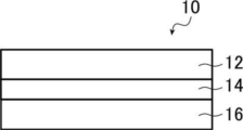
- FIG. 1 is a schematic cross-sectional view showing an example of an optical film.
- each component may use the substance applicable to each component individually by 1 type, or may use 2 or more types together.
- the content of the component refers to the total content of the substances used in combination unless otherwise specified.
- the bonding direction of the divalent group (eg, —O— CO— ) represented in this specification is not particularly limited .
- L 2 is *1-O—CO-*2, where *1 is the position bonded to the L1 side and * 2 is the position bonded to the L3 side. may be *1-CO-O-*2.
- Re( ⁇ ) and Rth( ⁇ ) represent in-plane retardation and thickness direction retardation at wavelength ⁇ , respectively.
- the wavelength ⁇ is 550 nm unless otherwise specified.
- the liquid crystal composition of the present invention is a liquid crystal composition containing a liquid crystal compound and a surfactant.
- the surfactant contained in the liquid crystal composition of the present invention (hereinafter also abbreviated as "specific surfactant”) has a structure represented by formula (Ia) described later (hereinafter also abbreviated as "branched Si structure” ) and two or more ring structures consisting of a cycloalkane ring or a monocyclic aromatic ring, and at least one of the ring structures is a ring structure consisting of a monocyclic aromatic ring. It is a copolymer having the unit B and
- the specific surfactant has a repeating unit A having two or more branched Si structures and a repeating unit B containing two or more predetermined ring structures, thereby reducing the surface tension of the liquid crystal composition and It is thought that, because of the good compatibility with the liquid crystal compound, cissing during formation of the liquid crystal cured layer was suppressed, and a liquid crystal cured layer excellent in orientation could be formed.
- the liquid crystal composition of the present invention will be described in detail below.
- any liquid crystal compound can be used in the present invention, it is preferable to use a rod-like liquid crystal compound or a discotic liquid crystal compound (discotic liquid crystal compound). Two or more kinds of rod-like liquid crystal compounds, two or more kinds of discotic liquid crystal compounds, or mixtures of rod-like liquid crystal compounds and discotic liquid crystal compounds may be used.
- rod-shaped liquid crystal compound for example, those described in claim 1 of JP-A-11-513019 or paragraphs [0026] to [0098] of JP-A-2005-289980 are preferable, and as the discotic liquid crystal compound, For example, those described in paragraphs [0020] to [0067] of JP-A-2007-108732 or paragraphs [0013] to [0108] of JP-A-2010-244038 are preferable. Moreover, you may use a reverse wavelength dispersion liquid crystal compound as a liquid crystal compound.
- R 11 , R 12 and R 13 each independently represent an alkyl group, an alkenyl group, an aryl group or an alkylenearyl group.
- the alkyl group includes, for example, a linear alkyl group having 1 to 18 carbon atoms, a branched chain or a cyclic alkyl group having 3 to 18 carbon atoms. Specific examples include methyl group, ethyl group, propyl group, butyl group, isopropyl group, tert-butyl group, cyclohexyl group and the like.
- Alkenyl groups include, for example, alkenyl groups having 2 to 12 carbon atoms.
- aryl groups include aryl groups having 6 to 12 carbon atoms.
- aryl groups include a phenyl group, an ⁇ -methylphenyl group, a naphthyl group and the like.
- alkylenearyl groups include alkylenearyl groups having 7 to 30 carbon atoms.
- the repeating unit A preferably contains 3 or more structures represented by the above formula (Ia) because the surface tension of the liquid crystal composition is reduced and unevenness can be suppressed during the formation of the liquid crystal cured layer.
- 3 to 6 are included.
- the surface tension of the liquid crystal composition is reduced, and unevenness can be suppressed during the formation of the liquid crystal cured layer.
- both the repeating unit A and the repeating unit B described below are preferably repeating units containing a structure represented by the following formula (Ib).
- R21 and R22 each independently represent a hydrogen atom or an alkyl group.
- R 23 represents a hydrogen atom or a substituent.
- L 1 represents -O- or -NR Z -.
- R Z represents a hydrogen atom or a substituent.
- R 11 , R 12 and R 13 each independently represent an alkyl group, an alkenyl group, an aryl group or an alkylenearyl group.
- L 2 and m are the same as defined in formula (a1) described later.
- R 23 is preferably an alkyl group, more preferably a linear alkyl group having 1 to 4 carbon atoms, and even more preferably a methyl group or an ethyl group.
- R 23 is preferably a hydrogen atom or a methyl group.
- the substituent representing the substituent represented by one embodiment of R Z is preferably an alkyl group, and a linear alkyl group having 1 to 4 carbon atoms. is more preferred, and a methyl group or an ethyl group is even more preferred.
- L 1 is preferably -O- or -NH-, more preferably -O-.
- the surface tension of the liquid crystal composition is reduced while maintaining the compatibility with the liquid crystal compound, and unevenness can be suppressed during the formation of the liquid crystal cured layer.
- ) is preferably a repeating unit.
- R 21 , R 22 and R 23 and L 1 are the same as those described in formula (Ib) above.
- R 11 , R 12 and R 13 are the same as those described in formula (Ia) above.
- the plurality of R 11 may be the same or different, the plurality of R 12 may be the same or different, and the plurality of R 13 may be the same. can be different.
- m represents an integer of 2 or more.
- L 2 represents an m+1 valent linking group.
- m is preferably an integer of 3 or more, more preferably an integer of 3-6, and even more preferably an integer of 3-5.
- repeating unit A examples include repeating units corresponding to monomers (monomers) represented by formulas K-1 to K-22 below.
- monomers represented by formulas K-1 to K-22 below.
- monomer K-1 the monomer represented by the following formula K-1 is referred to as "monomer K-1". The same applies to other monomers.
- the repeating unit B of the specific copolymer contains two or more ring structures consisting of a cycloalkane ring or a monocyclic aromatic ring, and at least one of the ring structures is a repeating ring structure consisting of a monocyclic aromatic ring. be.
- a cyclohexane ring is preferred, a 1,4-cyclohexylene group is more preferred, and a trans-1,4-cyclohexylene group is even more preferred.
- a monocyclic aromatic ring refers to a monocyclic aromatic ring that is not condensed or an individual monocyclic aromatic ring in a condensed ring. That is, the phenyl group is a group having one monocyclic aromatic benzene ring, and the naphthyl group is a group having two monocyclic aromatic benzene rings.
- the number of atoms constituting the monocyclic aromatic ring is not particularly limited, but may be about 5 to 18, preferably 5 to 10, more preferably 5 to 6.
- the monocyclic aromatic ring may be an aromatic ring consisting only of carbon, or a heteroaromatic ring containing an element other than carbon in the ring structure.
- Aromatic rings include benzene rings.
- Heteroaromatic rings include aromatic rings containing one or more atoms selected from sulfur, nitrogen and oxygen atoms. As the heteroaromatic ring, one containing a sulfur atom is preferable, and one containing one sulfur atom is more preferable.
- the repeating unit B is represented by any one of the following formulas (b1) to (b4) for the reason that the compatibility with the liquid crystal compound is improved and repelling is further suppressed during the formation of the liquid crystal cured layer.
- R 21 , R 22 and R 23 and L 1 are the same as explained in the above formula (Ib).
- R 24 and R 25 are each independently defined as defined for R 21 and R 22 in formula (Ib) above, and preferred embodiments are also the same.
- R 26 has the same definition as R 23 in formula (Ib) above, and the preferred embodiments are also the same.
- L 2 has the same definition as L 1 in formula (Ib) above, and the preferred embodiments are also the same.
- SP 1 and SP 2 each independently represent a spacer group.
- SP3 represents a single bond or a divalent linking group.
- Ph 1 represents a ring structure containing two or more monocyclic aromatic rings.
- M 1 represents a mesogenic group.
- T 1 represents a terminal group.
- D b4 represents a mesogenic group derived from a discotic liquid crystal.
- n4 is an integer of 3 or more and 8 or less, and is equal to the valence of Db4 .
- the spacer group represented by SP 1 and SP 2 is not particularly limited as long as it is a divalent linking group that does not contain a ring structure.
- 20 divalent aliphatic hydrocarbon groups and the like are used as the divalent aliphatic hydrocarbon group having 1 to 20 carbon atoms.
- an alkylene group having 1 to 15 carbon atoms is preferable, and an alkylene group having 1 to 8 carbon atoms is more preferable.
- methylene group, ethylene group, propylene group, butylene group, pentylene group, hexylene group, methylhexylene group, heptylene group and the like are preferably mentioned.
- one of -CH 2 - constituting a part of the divalent hydrocarbon group or two or more non-adjacent -CH 2 - are each independently -O-, -S -, -NH-, or -N(Q)- may be substituted.
- the substituent represented by Q is preferably an alkyl group, more preferably a linear alkyl group having 1 to 4 carbon atoms, and still more preferably a methyl group or an ethyl group.
- the spacer group is preferably a group represented by *-(CH 2 ) n1 -O-*.
- n1 represents an integer of 2 to 4
- * represents the binding position with L 1 or Ph 1 (M 1 ).
- R 7 represents a hydrogen atom or a substituent (preferably an alkyl group, more preferably a linear alkyl group having 1 to 4 carbon atoms).
- divalent linking group for example, -O-CO- (a divalent cyclic group having 5 to 8 atoms), -O- (alkylene group having 1 to 12 carbon atoms) -, - (5 atoms to 8 divalent cyclic group) -(bivalent cyclic group having 5 to 8 atoms) -(alkylene group having 1 to 12 carbon atoms) -CO-O-(alkylene group having 1 to 12 carbon atoms)- etc., but not limited to these.
- the ring structure containing two or more monocyclic aromatic rings represented by Ph 1 includes, for example, a naphthyl group and a biphenyl group, which may have a substituent, and among them, a naphthyl group. is preferred.
- the substituent is preferably an alkyl group, more preferably a linear alkyl group having 1 to 4 carbon atoms, and even more preferably a methyl group or an ethyl group.
- the mesogenic group represented by M1 is a group showing the main skeleton of liquid crystal molecules that contributes to liquid crystal formation.
- Liquid crystal molecules exhibit liquid crystallinity, which is an intermediate state (mesophase) between a crystalline state and an isotropic liquid state.
- the mesogenic group is preferably, for example, a group having at least one cyclic structure selected from the group consisting of aromatic hydrocarbon groups, heterocyclic groups and alicyclic groups.
- the mesogenic group is preferably a group having an aromatic hydrocarbon group or a group having an alicyclic group, which may have a substituent, for the reason that the orientation degree of the liquid crystal cured layer is improved.
- a group having one aromatic hydrocarbon group is more preferred, and a group having three aromatic hydrocarbon groups is even more preferred.
- the substituents are preferably alkyl groups, alkoxy groups, alkyl ester groups and acetyl groups, and more preferably methyl groups, tert-butyl groups, methoxy groups and methyl ester groups.
- M 1 in the above formulas (b2) and (b3) preferably represents a mesogenic group represented by the following formula (M1-A) for the reason that repelling is further suppressed during the formation of the liquid crystal cured layer. .
- the substituent which the divalent aromatic ring group may have is preferably an alkyl ester group, an alkyl group, an acetyl group, a methyl ester group, or a linear alkyl group having 1 to 4 carbon atoms. is more preferred, and a methyl group or an ethyl group is even more preferred.
- R 1 to R 5 each independently represent a hydrogen atom, a fluorine atom, or an alkyl group having 1 to 12 carbon atoms.
- the mesogenic group (D b4 ) derived from the discotic liquid crystal compound preferably has a structure represented by the following general formula (I) or formulas (D2) to (D13) described later. .
- L D1 , L D2 and L D3 each independently represent a single bond or a divalent linking group
- H 1 , H 2 and H 3 each independently represent general formula (IA ).
- L D1 , L D2 and L D3 each independently represent a single bond or a divalent linking group.
- R 7 represents a hydrogen atom or a substituent (preferably an alkyl group, more preferably a linear alkyl group having 1 to 4 carbon atoms).
- the divalent cyclic group in L D1 , L D2 and L D3 is a divalent linking group having at least one type of cyclic structure (hereinafter sometimes referred to as a cyclic group).
- the cyclic group is preferably a 5-, 6-, or 7-membered ring, more preferably a 5- or 6-membered ring, and most preferably a 6-membered ring.
- a ring contained in the cyclic group may be a condensed ring. However, a monocyclic ring is more preferable than a condensed ring.
- the ring contained in the cyclic group may be any of an aromatic ring, an aliphatic ring, and a heterocyclic ring.
- Preferred examples of the aromatic ring include a benzene ring and a naphthalene ring.
- a preferred example of the aliphatic ring is a cyclohexane ring.
- the heterocyclic ring is preferably a ring containing at least one sulfur atom, nitrogen atom or oxygen atom, and preferable examples thereof include pyridine ring, pyrimidine ring and oxadiazole ring.
- the cyclic group is more preferably an aromatic ring and a heterocyclic ring.
- the divalent cyclic group in the present invention is more preferably a divalent linking group consisting only of a cyclic structure (including a substituent).
- cyclic group having a pyrimidine ring a pyrimidine-2,5-diyl group is preferred.
- cyclic group having an oxadiazole ring a 1,2,4-oxadiazole-3,5-diyl group is preferred.
- the specific copolymer may have repeating units C other than those described above as long as the effects of the invention are not impaired.
- monomers forming the repeating unit C other than the above include acrylic acid, methacrylic acid, acrylic acid ester compounds, methacrylic acid ester compounds, maleimide compounds, acrylamide compounds, methacrylamide compounds, acrylonitrile, maleic anhydride, Examples include styrene compounds and vinyl compounds.
- the content of the specific surfactant is preferably 0.01 to 10% by mass, preferably 0.02 to 1%, based on the total solid content (100% by mass) of the liquid crystal composition, from the viewpoint that the effect of the present invention is more excellent. % by mass is more preferred, and 0.04 to 0.5% by mass is even more preferred.
- the weight average molecular weight (Mw) of the specific surfactant is preferably 10,000 to 40,000, more preferably 11,000 to 39,000, even more preferably 13,000 to 35,000.
- Mw weight average molecular weight
- the weight average molecular weight in the present invention is a value measured by a gel permeation chromatography (GPC) method.
- the liquid crystal composition of the present invention preferably contains a solvent.
- solvents include ketones (eg, acetone, 2-butanone, methylethylketone, methylisobutylketone, cyclopentanone, and cyclohexanone), ethers (eg, dioxane, tetrahydrofuran, tetrahydropyran, dioxolane, tetrahydrofurfuryl alcohol, and cyclopentyl methyl ether, etc.), aliphatic hydrocarbons (e.g., hexane, etc.), alicyclic hydrocarbons (e.g., cyclohexane, etc.), aromatic hydrocarbons (e.g., benzene, toluene, xylene, and , trimethylbenzene, etc.), halogenated carbons (e.g., dichloromethane, trichloromethane
- ethers eg., di
- solvents it is preferable to use an organic solvent, and more preferable to use ketones and/or esters, because the orientation of the cured liquid crystal layer to be formed is improved and the heat resistance is further improved. .
- the liquid crystal composition of the invention may contain a polymerization initiator.
- the polymerization initiator is not particularly limited, it is preferably a compound having photosensitivity, that is, a photopolymerization initiator.
- Various compounds can be used as the photopolymerization initiator without any particular limitation. Examples of photoinitiators include ⁇ -carbonyl compounds, acyloin ethers, ⁇ -hydrocarbon-substituted aromatic acyloin compounds, polynuclear quinone compounds, combinations of triarylimidazole dimers and p-aminophenyl ketones, acridine and phenazine compounds.
- oxadiazole compounds o-acyloxime compounds
- acylphosphine oxide compounds oxadiazole compounds
- commercially available products can also be used, and BASF Irgacure-184, Irgacure-907, Irgacure-369, Irgacure-651, Irgacure-819, Irgacure-OXE-01 and Irgacure- OXE-02 and the like.
- the content of the polymerization initiator is preferably 0.01 to 30% by mass, preferably 0.1 to 30% by mass, based on the total solid content (100% by mass) of the liquid crystal composition. 15% by mass is more preferred.
- the liquid crystal composition may contain a chiral agent.
- the chiral agent may be selected depending on the purpose, since the helical twist direction or helical pitch induced by the compound differs.
- the chiral agent is not particularly limited, and known compounds (for example, Liquid Crystal Device Handbook, Chapter 3, Section 4-3, TN (twisted nematic), STN (Super Twisted Nematic) chiral agent, page 199, Japan Society for the Promotion of Science) 142nd Committee, ed., 1989), isosorbide, isomannide derivatives, and the like can be used.
- Chiral agents generally contain an asymmetric carbon atom, but axially chiral compounds or planar chiral compounds that do not contain an asymmetric carbon atom can also be used as chiral agents.
- Examples of axially or planarly chiral compounds include binaphthyl, helicene, paracyclophane, and derivatives thereof.
- the chiral agent may have a polymerizable group.
- the polymerizable group of the chiral agent is preferably an unsaturated polymerizable group, an epoxy group or an aziridinyl group, more preferably an unsaturated polymerizable group, and more preferably an ethylenically unsaturated polymerizable group. preferable.
- a chiral agent may have a photoisomerization site.
- the photoisomerization site is preferably a cinnamoyl site, a chalcone site, an azobenzene site or a stilbene site, more preferably a cinnamoyl site, a chalcone site or a stilbene site.
- Specific compounds of the chiral agent include optically active isosorbide derivatives described in paragraphs 0015 to 0049 of JP-A-2003-313187, optically active isomannide derivatives described in paragraphs 0015-0057 of JP-A-2003-313188, Optically active polyesters/amides described in paragraphs 0015 to 0052 of JP-A-2003-313292, chiral agents described in paragraphs 0012 to 0053 of WO2018/194157, and the like.
- the content of the optional chiral agent is preferably 5.0% by mass or less, more preferably 3.0% by mass or less, relative to the total mass of the liquid crystal compound, in that the liquid crystal compound is easily orientated uniformly. 0% by mass or less is more preferable, and less than 1.0% by mass is particularly preferable. Although the lower limit is not particularly limited, it is preferably 0.01% by mass or more, more preferably 0.02% by mass or more, and even more preferably 0.05% by mass or more.
- a chiral agent may be used individually by 1 type, or may use 2 or more types together. When two or more chiral agents are used in combination, the total content is preferably within the above range.
- the chiral agent used in the liquid crystal composition includes a chiral agent A and a chiral agent B that induces a spiral in the opposite direction to that of the chiral agent A. It is preferred to use two or more chiral agents. For example, when the helix induced by chiral agent A is rightward, the helix induced by chiral agent B is leftward.
- the cured liquid crystal layer of the present invention is a cured liquid crystal layer obtained by fixing the alignment state of the above liquid crystal composition of the present invention.
- Examples of the method for forming the cured liquid crystal layer include a method in which the above-described liquid crystal composition of the present invention is used to form a desired alignment state, and then fixed by polymerization.
- the polymerization conditions are not particularly limited, but it is preferable to use ultraviolet rays in the polymerization by light irradiation.
- the irradiation dose is preferably 10 mJ/cm 2 to 50 J/cm 2 , more preferably 20 mJ/cm 2 to 5 J/cm 2 , still more preferably 30 mJ/cm 2 to 3 J/cm 2 , particularly 50 to 1000 mJ/cm 2 . preferable.
- it may be carried out under heating conditions.
- the liquid crystal cured layer can be formed on an arbitrary support or alignment film in the optical film described later, or on the polarizer in the polarizing plate described later.
- the alignment state of the liquid crystal compound in the liquid crystal cured layer of the present invention may be any of horizontal alignment, vertical alignment, tilt alignment, and twist alignment. Further, as described in WO2021/033640, a first region in which the alignment state of the liquid crystal compound is twisted along the helical axis extending along the thickness direction is fixed, and the alignment state of the liquid crystal compound is homogeneously aligned is fixed.
- One layer may have a plurality of alignment states, such as a liquid crystal cured layer having a second region along the thickness direction.
- the term “horizontal alignment” refers to the main surface of the liquid crystal cured layer (or the surface of the member when the liquid crystal cured layer is formed on a member such as a support and an alignment film), and the liquid crystal It means parallel to the longitudinal direction of the compound. It should be noted that it is not required to be strictly parallel, and in this specification, it means that the orientation is such that the angle formed by the major axis direction of the liquid crystal compound and the main surface of the liquid crystal cured layer is less than 10 °.
- the cured liquid crystal layer of the present invention is preferably an optically anisotropic layer.
- the optically anisotropic layer includes a positive A plate, a positive C plate, a first region in which the orientation state of a liquid crystal compound twisted along a helical axis extending along the thickness direction is fixed, and a homogeneously oriented liquid crystal compound.
- An optically anisotropic layer (hereinafter also referred to as "optically anisotropic layer A”) having a second region formed by fixing the alignment state of a liquid crystal compound along the thickness direction.
- the positive A plate (positive A plate) and the positive C plate (positive C plate) are defined as follows.
- nx is the refractive index in the film in-plane slow axis direction (the direction in which the in-plane refractive index is maximized)
- ny is the refractive index in the direction perpendicular to the in-plane slow axis
- the refraction in the thickness direction When the rate is nz, the positive A plate satisfies the relationship of formula (A1), and the positive C plate satisfies the relation of formula (C1).
- the positive A plate shows a positive Rth value, and the positive C plate shows a negative Rth value.
- Formula (A1) nx>ny ⁇ nz Formula (C1) nz>nx ⁇ ny Note that the above “ ⁇ ” includes not only the case where both are completely the same, but also the case where both are substantially the same. Regarding this “substantially the same”, for a positive A plate, for example, (ny ⁇ nz) ⁇ d (where d is the thickness of the film) is ⁇ 10 to 10 nm, preferably ⁇ 5 to 5 nm. is also included in “ny ⁇ nz”, and the case where (nx ⁇ nz) ⁇ d is ⁇ 10 to 10 nm, preferably ⁇ 5 to 5 nm is also included in “nx ⁇ nz”. In addition, for a positive C plate, for example, (nx ⁇ ny) ⁇ d (where d is the thickness of the film) is 0 to 10 nm, preferably 0 to 5 nm. .
- Re (550) is preferably 100 to 180 nm, more preferably 120 to 160 nm, 130 to 150 nm is more preferred, and 130 to 145 nm is particularly preferred.
- the " ⁇ / 4 plate” is a plate having a ⁇ / 4 function, specifically, the function of converting linearly polarized light of a certain wavelength into circularly polarized light (or circularly polarized light into linearly polarized light) is a plate with
- a first region in which the alignment state of a liquid crystal compound twisted along a helical axis extending along the thickness direction is fixed, and a second region in which the alignment state of a homogeneously aligned liquid crystal compound is fixed are arranged in the thickness direction.
- the optically anisotropic layer (optically anisotropic layer A) provided along .
- the thickness of the first region of the optically anisotropic layer A is d1 (nm) and the refractive index anisotropy of the first region measured at a wavelength of 550 nm is ⁇ n1
- the optically anisotropic layer is suitable for a circularly polarizing plate.
- the first region preferably satisfies the following formula (1-1) in that it can be applied to Formula (1-1) 100 nm ⁇ n1d1 ⁇ 240 nm Among them, it is more preferable to satisfy formula (1-2), and more preferable to satisfy formula (1-3).
- Formula (1-2) 120 nm ⁇ n1d1 ⁇ 220 nm
- Formula (1-3) 140 nm ⁇ n1d1 ⁇ 200 nm
- the refractive index anisotropy ⁇ n1 means the refractive index anisotropy of the first region.
- the absolute value of the twist angle of the liquid crystal compound in the first region is not particularly limited, it is preferably 60 to 120°, more preferably 70 to 110°, in that the optically anisotropic layer can be suitably applied to the circularly polarizing plate.
- the torsion angle is measured using Axoscan manufactured by Axometrics using the company's device analysis software.
- the optically anisotropic layer is a circularly polarizing plate.
- the second region preferably satisfies the following formula (2-1) because it can be suitably applied to Formula (2-1) 100 nm ⁇ n2d2 ⁇ 240 nm Among them, it is more preferable to satisfy formula (2-2), and more preferable to satisfy formula (2-3).
- Formula (2-2) 120 nm ⁇ n2d2 ⁇ 220 nm
- Formula (2-3) 140 nm ⁇ n2d2 ⁇ 200 nm
- the refractive index anisotropy ⁇ n2 means the refractive index anisotropy of the second region.
- the optical film of the invention is an optical film having the liquid crystal cured layer of the invention.
- the structure of the optical film will be described with reference to FIG.
- FIG. 1 is a schematic cross-sectional view showing an example of an optical film. It should be noted that FIG. 1 is a schematic diagram, and the relationship of thickness and position of each layer does not necessarily match the actual one, and both the support and the alignment film shown in FIG. 1 are arbitrary constituent members.
- the optical film 10 shown in FIG. 1 has a support 16, an alignment film 14, and a liquid crystal cured layer 12 as a cured product of the liquid crystal composition of the present invention in this order.
- the liquid crystal cured layer 12 may be a laminate of two or more different liquid crystal cured layers.
- the polarizing plate of the present invention which will be described later, is used as a circular polarizing plate, or when the optical film of the present invention is used in an IPS (In-Plane-Switching) or FFS (Fringe-Field-Switching) liquid crystal display device.
- IPS In-Plane-Switching
- FFS Frringe-Field-Switching
- the liquid crystal cured layer may be peeled off from the support and the liquid crystal cured layer alone may be used as an optical film.
- Various members used in the optical film will be described in detail below.
- the liquid crystal cured layer of the optical film of the present invention is the liquid crystal cured layer of the present invention described above.
- the thickness of the liquid crystal cured layer is not particularly limited, but is preferably 0.1 to 10 ⁇ m, more preferably 0.5 to 5 ⁇ m.
- the optical film may have a support as a substrate for forming the liquid crystal cured layer, as described above.
- Such supports are preferably transparent.
- the light transmittance is preferably 80% or more.
- Such supports include, for example, glass substrates and polymeric films.
- Materials for the polymer film include cellulose-based polymers; acrylic polymers having acrylic acid ester polymers such as polymethyl methacrylate and lactone ring-containing polymers; thermoplastic norbornene-based polymers; polycarbonate-based polymers; Polyester-based polymers such as phthalate; Styrene-based polymers such as polystyrene and acrylonitrile-styrene copolymers (AS resins); Polyolefin-based polymers such as polyethylene, polypropylene, and ethylene-propylene copolymers; Vinyl chloride-based polymers; and amide-based polymers such as aromatic polyamides; imide-based polymers; sulfone-based polymers; polyethersulfone-based polymers; polyetheretherketone-based polymers; arylate-based polymers; polyoxymethylene-based polymers; epoxy-based polymers; and polymers obtained by mixing these polymers.
- the thickness of the support is not particularly limited, it is preferably 5 to 100 ⁇ m, more preferably 5 to 50 ⁇ m.
- the support is peelable.
- the liquid crystal cured layer is preferably formed on the surface of the alignment film.
- the alignment film may be sandwiched between the support and the liquid crystal cured layer.
- the above-described support may also serve as an alignment film.
- the alignment film may be any film as long as it has a function of aligning the polymerizable liquid crystal compound contained in the composition.
- the alignment film generally contains a polymer as a main component.
- Polymer materials for alignment films are described in many documents, and many commercial products are available.
- Polyvinyl alcohol, polyimide, or any derivative thereof is preferable as the polymer material for the alignment film, and denatured or undenatured polyvinyl alcohol is more preferable.
- the photo-alignment film is not particularly limited, but an alignment film formed of polymer materials such as polyamide compounds and polyimide compounds described in paragraphs [0024] to [0043] of WO 2005/096041; A liquid crystal alignment film formed from a liquid crystal alignment agent having a cinnamoyl group described in JP-A-155308;
- the thickness of the alignment film is not particularly limited, it is preferably 0.01 to 10 ⁇ m, more preferably 0.01 to 1 ⁇ m, from the viewpoint of alleviating surface irregularities that may exist on the support and forming a liquid crystal cured layer with a uniform thickness. More preferably, 0.01 to 0.5 ⁇ m is even more preferable.
- the liquid crystal cured layer of the present invention may be formed on the surface of another liquid crystal cured layer, or another liquid crystal cured layer may be formed on the surface of the liquid crystal cured layer of the present invention.
- other cured liquid crystal layers include, for example, a cured liquid crystal layer obtained by fixing the above-described liquid crystal composition of the present invention in a desired alignment state.
- a liquid crystal cured layer (light absorption anisotropic film) formed by fixing the alignment state of a composition containing the above-described liquid crystal compound, polymerization initiator, dichroic substance, surfactant, solvent, etc. .
- the optical film may contain an ultraviolet (UV) absorber in consideration of the influence of external light (especially ultraviolet light).
- the ultraviolet absorber may be contained in the liquid crystal cured layer, or may be contained in members other than the liquid crystal cured layer constituting the optical film.
- a support is suitable.
- the ultraviolet absorber any conventionally known one capable of exhibiting ultraviolet absorbency can be used.
- benzotriazole-based or hydroxyphenyltriazine-based UV absorbers are preferable from the viewpoint of obtaining UV absorbability (UV-blocking capability) used in image display devices because of their high UV absorbency.
- Tinuvin400 Tinuvin405, Tinuvin460, Tinuvin477, Tinuvin479, and Tinuvin1577 (all manufactured by BASF) can be used.
- the polarizing plate of the present invention has the optical film of the present invention described above and a polarizer.
- the liquid crystal cured layer (optically anisotropic layer) of the optical film is a positive A plate, it can be suitably applied to a circularly polarizing plate or the like.
- the angle formed is preferably 30 to 60°, more preferably 40 to 50°, still more preferably 42 to 48°, and particularly preferably 45°.
- the "slow axis" means the direction in which the refractive index is maximized in the plane of the liquid crystal cured layer
- the "absorption axis" of the polarizer means the direction in which the absorbance is highest.
- the optically anisotropic layer A can be suitably applied to a circularly polarizing plate or the like, and the homogeneously aligned liquid crystal compound
- the absolute value of the angle between the in-plane slow axis of the second region and the absorption axis of the polarizer is preferably 5 to 25°, more preferably 10 to 20°.
- the polarizing plate can also be used as an optical compensation film for an IPS or FFS liquid crystal display device.
- the optically anisotropic layer described above is at least one plate of a laminate of a positive A plate and a positive C plate.
- the angle formed by the slow axis of the plate layer and the absorption axis of the polarizer described later is preferably orthogonal or parallel.
- the slow axis of the positive A plate layer and the absorption axis of the polarizer described later More preferably, the angle with the axis is 0-5° or 85-95°.
- the angle formed by the slow axis of the cured liquid crystal layer and the absorption axis of the polarizer described later is preferably parallel or orthogonal.
- parallel does not strictly require parallelism, but means that the angle between one and the other is less than 10°.
- perpendicular does not require that they are strictly perpendicular, but means that the angle between one and the other is more than 80° and less than 100°.
- the polarizer is not particularly limited as long as it is a member having a function of converting light into specific linearly polarized light, and conventionally known absorptive polarizers, reflective polarizers, and coated polarizers can be used.
- As the absorbing polarizer an iodine-based polarizer, a dye-based polarizer using a dichroic dye, a polyene-based polarizer, or the like is used.
- Iodine-based polarizers and dye-based polarizers include coating-type polarizers and stretching-type polarizers, and both can be applied. child is preferred.
- coated polarizers include polarizers containing a cured liquid crystal compound and a dichroic dye.
- polarizers containing a cured liquid crystal compound and a dichroic dye examples include polarizers containing a cured liquid crystal compound and a dichroic dye.
- the reflective polarizer a polarizer in which thin films having different birefringences are laminated, a wire grid polarizer, and a polarizer in which a cholesteric liquid crystal having a selective reflection region and a quarter wavelength plate are combined are used.
- the thickness of the polarizer is not particularly limited, it is preferably 3 to 60 ⁇ m, more preferably 3 to 30 ⁇ m, even more preferably 3 to 10 ⁇ m.
- an adhesive layer may be arranged between the liquid crystal cured layer in the optical film and the polarizer.
- adhesives include, but are not limited to, polyvinyl alcohol-based adhesives.
- the polarizing plate may have an adhesive layer disposed between the liquid crystal cured layer and the polarizer in the optical film.
- a curable adhesive composition that is cured by irradiation with active energy rays or by heating is preferred.
- the curable adhesive composition include a curable adhesive composition containing a cationic polymerizable compound and a curable adhesive composition containing a radically polymerizable compound.
- the thickness of the adhesive layer is preferably 0.01 to 20 ⁇ m, more preferably 0.01 to 10 ⁇ m, even more preferably 0.05 to 5 ⁇ m.
- the thickness of the adhesive layer is within this range, no lifting or peeling occurs between the laminated protective layer or liquid crystal cured layer and the polarizer, and practically acceptable adhesive strength can be obtained. Moreover, the thickness of the adhesive layer is preferably 0.4 ⁇ m or more from the viewpoint of suppressing the generation of air bubbles.
- the adhesive layer for example, paragraphs [0062] to [0080] of JP-A-2016-35579 can be referred to, the contents of which are incorporated herein.
- the polarizing plate may have an easily adhesive layer disposed between the liquid crystal cured layer and the polarizer in the optical film.
- the storage elastic modulus of the easily adhesive layer at 85° C. is 1.0 ⁇ 10 6 Pa to 1.0 ⁇ 10 6 Pa to 1.0 ⁇ 10 6 Pa. It is preferably 0 ⁇ 10 7 Pa.
- constituent materials of the easy-adhesion layer include polyolefin-based components and polyvinyl alcohol-based components.
- the thickness of the easy-adhesion layer is preferably 500 nm to 1 ⁇ m.
- paragraphs [0048] to [0053] of JP-A-2018-36345 can be referred to, the contents of which are incorporated herein.
- the image display device of the present invention is an image display device having the optical film of the present invention or the polarizing plate of the present invention.
- the display element used in the image display device is not particularly limited, and examples thereof include liquid crystal cells, organic electroluminescence (hereinafter abbreviated as "EL (Electro Luminescence)”) display panels, and plasma display panels. Among these, liquid crystal cells and organic EL display panels are preferred.
- a liquid crystal display device which is an example of an image display device, is a liquid crystal display device having the above-described polarizing plate and a liquid crystal cell.
- the above-described polarizing plate is preferably used as the front-side polarizing plate, and more preferably the above-described polarizing plates are used as the front-side and rear-side polarizing plates.
- Liquid crystal cells used in liquid crystal display devices are VA (Vertical Alignment) mode, OCB (Optically Compensated Bend) mode, IPS (In-Plane-Switching) mode, FFS (Fringe-Field-Switching) mode, or TN (Twisted Bend) mode. Nematic) mode is preferred, but not limited to these.
- Organic EL display device An example of an organic EL display device, which is an example of an image display device, is a mode having, from the viewing side, a polarizer, a ⁇ /4 plate made of the liquid crystal cured layer described above, and an organic EL display panel in this order. be done. Also, the organic EL display panel is a display panel configured using an organic EL element in which an organic light-emitting layer (organic electroluminescence layer) is sandwiched between electrodes (between a cathode and an anode). The configuration of the organic EL display panel is not particularly limited, and a known configuration is adopted.
- Example 1 [Preparation of cellulose acylate film (substrate)] The following composition was put into a mixing tank, stirred, and heated at 90° C. for 10 minutes. Thereafter, the resulting composition was filtered through a filter paper with an average pore size of 34 ⁇ m and a sintered metal filter with an average pore size of 10 ⁇ m to prepare a dope.
- the solid content concentration of the dope was 23.5% by mass
- the amount of the plasticizer added was the ratio to the cellulose acylate
- Cellulose acylate dope Cellulose acylate (acetyl substitution degree 2.86, viscosity average polymerization degree 310) 100 parts by mass sugar ester compound 1 (represented by chemical formula (S4)) 6.0 parts by mass sugar ester compound 2 (represented by chemical formula (S5)) 2.0 parts by mass silica particle dispersion (AEROSIL R972, Nippon Aerosil Co., Ltd.) made) 0.1 part by mass solvent (methylene chloride/methanol/butanol) ⁇
- the dope prepared above was cast using a drum film-forming machine.
- the dope was cast from a die in contact with a metal support cooled to 0° C., after which the resulting web (film) was stripped off.
- the drum was made of SUS (steel use stainless).
- the web (film) obtained by casting is peeled off from the drum, and dried for 20 minutes in a tenter device using a tenter device in which both ends of the web are clipped and conveyed at 30 to 40 ° C. during film transportation. bottom. Subsequently, the web was post-dried by zone heating while being rolled. The resulting web was knurled and wound up.
- the resulting cellulose acylate film had a thickness of 40 ⁇ m, an in-plane retardation Re(550) of 1 nm at a wavelength of 550 nm, and a thickness direction retardation Rth(550) of 26 nm at a wavelength of 550 nm.
- ⁇ Alkaline saponification treatment> The above-described cellulose acylate film was passed through a dielectric heating roll at a temperature of 60°C to raise the film surface temperature to 40°C, and then an alkaline solution having the composition shown below was applied to the band surface of the film using a bar coater.
- the coating was applied at a coating amount of 14 ml/m 2 by means of a vacuum cleaner, and conveyed for 10 seconds under a steam type far-infrared heater manufactured by Noritake Co., Ltd. which was heated to 110°C. Subsequently, using the same bar coater, 3 ml/m 2 of pure water was applied. Next, after repeating water washing with a fountain coater and draining with an air knife three times, the film was transported to a drying zone at 70° C. for 10 seconds and dried to prepare a cellulose acylate film saponified with an alkali.
- Alignment film coating solution The following modified polyvinyl alcohol-1 10 parts by mass Water 170 parts by mass Methanol 57 parts by mass ⁇ ⁇
- Modified polyvinyl alcohol-1 (Wherein, the numerical value described in each repeating unit represents the content (mol%) of each repeating unit relative to all repeating units.)
- a liquid crystal composition (1) containing a rod-like liquid crystal compound having the following composition was applied using a Giesser coater to form a composition layer.
- the absolute value of the weighted average helical induced force of the chiral agent in the composition layer in step 1 was 0.0 ⁇ m ⁇ 1 .
- the resulting composition layer was then heated at 80° C. for 60 seconds. This heating oriented the rod-like liquid crystal compound in the composition layer in a predetermined direction. After that, the composition layer was irradiated with ultraviolet rays using a 365 nm LED lamp (manufactured by Acroedge Co., Ltd.) at 30° C.
- composition layer was heated at 80° C. for 10 seconds. Then, nitrogen purge was performed, and the composition layer was irradiated with ultraviolet rays using a metal halide lamp (manufactured by Eye Graphics Co., Ltd.) at 75 ° C. with an oxygen concentration of 100 volume ppm (irradiation amount: 500 mJ / cm 2 )
- a liquid crystal cured layer (optically anisotropic layer) was formed in which the alignment state of the liquid crystal compound was fixed. Thus, an optical film was produced.
- Liquid crystal composition (1) ⁇ The following rod-like liquid crystal compound (A) 80 parts by mass The following precipitation suppressing compound (A) 17 parts by mass The following precipitation suppressing compound (B) 3 parts by mass Ethylene oxide-modified trimethylolpropane triacrylate (V # 360, Osaka Organic Chemical ( Co., Ltd.) 4 parts by mass Photopolymerization initiator (Ominirad.819 IGM Resins B.I. V.
- Rod-shaped liquid crystal compound (A) [a mixture of the following liquid crystal compounds (RA), (RB) and (RC) at a ratio of 84:14:2 (mass ratio)]
- Precipitation suppression compound (A): Me represents a methyl group.
- Left-handed chiral agent (L1): Bu represents a methyl group.
- the optical film produced above was cut parallel to the rubbing direction, and the cured liquid crystal layer was observed from the cross-sectional direction with a polarizing microscope.
- the thickness of the liquid crystal cured layer is 2.6 ⁇ m, and the region (second region) with a thickness (d2) of 1.3 ⁇ m on the substrate side of the liquid crystal cured layer has a homogeneous alignment without a twist angle, and the air side of the liquid crystal cured layer ( In a region (first region) having a thickness (d1) of 1.3 ⁇ m on the side opposite to the substrate, the liquid crystal compound was twisted and oriented.
- the optical properties of the optical film were obtained using Axoscan from Axometrics and analysis software (Multi-Layer Analysis) from Axometrics.
- the product ( ⁇ n2d2) of ⁇ n2 and the thickness d2 (nm) at a wavelength of 550 nm in the second region is 178 nm, the twist angle of the liquid crystal compound is 0°, and the orientation axis angle of the liquid crystal compound with respect to the longitudinal direction is in contact with the substrate. -11.0° on the side and -11.0° on the side in contact with the first region.
- the product ( ⁇ n1d1) of ⁇ n1 and thickness d1 (nm) in the first region at a wavelength of 550 nm was 180 nm
- the twist angle of the liquid crystal compound was 88°
- the orientation axis angle of the liquid crystal compound with respect to the longitudinal direction was The angle was ⁇ 11.0° on the side contacting the two regions and ⁇ 91.0° on the air side.
- the orientation axis angle of the liquid crystal compound contained in the liquid crystal cured layer was observed from the surface side of the liquid crystal cured layer with the longitudinal direction of the substrate being 0° as a reference, and the clockwise (right) rotation was negative. Counterclockwise (counterclockwise) time is represented as positive.
- the twisted structure of the liquid crystal compound is obtained by observing the substrate from the surface side of the liquid crystal cured layer, and based on the orientation axis direction of the liquid crystal compound on the surface side (front side), the liquid crystal compound on the substrate side (back side).
- the direction of the orientation axis is clockwise (right), it is indicated as negative, and when it is counterclockwise (left), it is indicated as positive.
- a polyvinyl alcohol (PVA) film having a thickness of 80 ⁇ m was dyed by immersing it in an iodine aqueous solution having an iodine concentration of 0.05% by mass at 30° C. for 60 seconds.
- the obtained film was longitudinally stretched to 5 times its original length while being immersed in an aqueous boric acid solution having a boric acid concentration of 4% by mass for 60 seconds, and dried at 50° C. for 4 minutes. , a polarizer having a thickness of 20 ⁇ m was obtained.
- polarizer protective film A commercially available cellulose acylate film, FUJITAC TG40UL (manufactured by Fuji Film Co., Ltd.), was prepared, immersed in a 1.5 mol/liter sodium hydroxide aqueous solution at 55°C, and then sufficiently added with water to remove sodium hydroxide. washed away. Thereafter, the obtained film was immersed in a 0.005 mol/liter aqueous solution of dilute sulfuric acid at 35° C. for 1 minute and then immersed in water to thoroughly wash off the dilute aqueous solution of sulfuric acid. Finally, the resulting film was sufficiently dried at 120° C. to produce a polarizer protective film having a saponified surface.
- the optical film produced above is subjected to a saponification treatment in the same manner as in the production of the polarizer protective film described above, and then the polarizer and polarizer protective film described above are attached to the substrate surface included in the optical film.
- a continuous circularly polarizing plate was produced by laminating them continuously using an alcohol-based adhesive. That is, the circularly polarizing plate had a polarizer protective film, a polarizer, a substrate, and a liquid crystal cured layer in this order.
- the absorption axis of the polarizer coincides with the longitudinal direction of the circularly polarizing plate, and the rotation angle of the in-plane slow axis of the second region with respect to the absorption axis of the polarizer is 11.0°.
- the rotation angle of the in-plane slow axis of the surface of the first region opposite to the second region side with respect to the absorption axis was 91.0°.
- the rotation angle of the in-plane slow axis is a positive angle value in the counterclockwise direction and a negative angle value in the clockwise direction when the liquid crystal cured layer is observed from the polarizer side and the longitudinal direction of the substrate is set to 0° as a reference. is represented by
- Examples 2 to 12 and Comparative Examples 1 and 2 Same as Example 1 except that the copolymer (No101) of Example 1 was changed to the copolymers (No102) to (No112) and (C-1) to (C-2) listed in Table 1 below. Liquid crystal compositions (2) to (12) and (C1) to (C2) were thus obtained. Further, using these liquid crystal compositions, a liquid crystal cured layer, an optical film, and a circularly polarizing plate were obtained in the same manner as in Example 1.
- Example 13 A liquid crystal cured layer, an optical film, and a circularly polarizing plate were obtained by the following procedures.
- a cellulose triacetate film TJ40 manufactured by Fuji Film Co., Ltd.: thickness 40 ⁇ m
- the same composition for forming a photo-alignment film as in Example 1 of WO2020/175620 was prepared and applied onto the support with a #3.0 wire bar. After that, it was dried with hot air at 60° C. for 60 seconds to prepare a coating film having a thickness of 300 nm.
- the prepared coating film was irradiated with ultraviolet rays using an ultra-high pressure mercury lamp in the atmosphere.
- the formed positive A plate 1 had a film thickness of 2.5 ⁇ m.
- Re(550) of the positive A plate 1 is 145 nm, Rth(550) is 73 nm, Re(550)/Re(450) is 1.13, Re(650)/Re(550) is 1.01, and the optical axis is The tilt angle was 0°, and the liquid crystal compound was homogeneously aligned. Thus, an optical film was produced.
- Example 14 to 17 Liquid crystal compositions (14) to (17) were prepared in the same manner as in Example 1, except that the copolymer (No. 101) in Example 1 was changed to the copolymers (No. 114) to (No. 117) shown in Table 1 below. got Further, using these liquid crystal compositions, a liquid crystal cured layer, an optical film, and a circularly polarizing plate were obtained in the same manner as in Example 1.
- Example 18 An optical film, And a circularly polarizing plate was obtained.
- a coating liquid R1 for a cholesteric liquid crystal layer having the following composition was prepared.
- ⁇ Coating liquid R1 for cholesteric liquid crystal layer ⁇ Discotic liquid crystal compound (Compound 101 below) 80 parts by mass Discotic liquid crystal compound (Compound 102 below) 20 parts by mass Polymerizable monomer 1 below 10 parts by mass Copolymer (No 118) 0.3 parts by mass Polymerization below Initiator 1 3 parts by mass Chiral agent 1 below 3.03 parts by mass Vertical alignment agent 1 below 0.2 parts by mass Methyl ethyl ketone 290 parts by mass Cyclohexanone 50 parts by mass ⁇
- the prepared cholesteric liquid crystal layer coating solution R1 was applied to a rubbed cellulose acylate film prepared in the same manner as in Example 1 using a bar coater. Subsequently, the coating film was dried at 70° C. for 2 minutes to evaporate the solvent, and then heat-aged at 115° C. for 3 minutes to obtain a uniform alignment state. Thereafter, this coating film was kept at 45° C. and irradiated with ultraviolet rays (300 mJ/cm 2 ) using a high-pressure mercury lamp in a nitrogen atmosphere to form a cholesteric liquid crystal layer R1 that reflects red right-handed circularly polarized light. A scanning electron microscope (SEM) observation of the cross section of the cholesteric liquid crystal layer R1 revealed that the film thickness was 2.8 ⁇ m. It was also confirmed that the cholesteric liquid crystal layer R1 was vertically aligned.
- SEM scanning electron microscope
- Example 19-20 A cholesteric liquid crystal layer R2 was formed in the same manner as in Example 18, except that copolymer (No. 118) was changed to copolymers (No. 119) to (No. 120) shown in Table 1 below. Next, an optical film and a circularly polarizing plate were obtained in the same manner as in Example 1, except that the cholesteric liquid crystal layer R2 was used as the liquid crystal cured layer.
- repelling means a region where the liquid crystal cured layer is not formed. Repelling occurs when an optical film containing a liquid crystal cured layer and a support not containing a liquid crystal cured layer are laminated with a 90° shift, and the sample is rotated when observed under crossed Nicols conditions using the transmission mode of a polarizing microscope. Refers to the part that remains dark even when the light is turned on. Based on the results, evaluation was made according to the following criteria. The results are shown in Table 1 below. A: No repelling B: 1 or more and less than 30 repelling C: 30 or more and less than 60 repelling D: 60 or more repelling
- Example 13 ⁇ Method for Observing Optical Film Produced in Example 13> The produced optical film was observed with a polarizing microscope in a state shifted by 2 degrees from the extinction position. A state in which there was no partial difference in brightness during observation was evaluated as uniformly oriented liquid crystal directors (excellent orientation). ⁇ Method for Observing Optical Films Produced in Examples 18 and 19> The orientation of the cholesteric layer of the produced optical film was confirmed by SEM observation and evaluated according to the following criteria. ⁇ Evaluation method> The results observed by the above observation method were classified according to the following criteria. The results are shown in Table 1 below. A: The liquid crystal directors are aligned finely and the display performance is very excellent. B: The liquid crystal directors are uniformly aligned and the display performance is excellent. C: The liquid crystal directors are partially disturbed and the surface state is stable. D: The liquid crystal director is greatly disturbed, the surface state is not stable, and the display performance is very poor.
- Example 1 it was found that when a specific surfactant was blended, repelling was suppressed during formation of the liquid crystal cured layer, and a liquid crystal cured layer excellent in alignment could be formed (Examples 1 to 19).
- Example 1 it was found that when the repeating unit A contained three or more structures represented by the above formula (Ia), unevenness was suppressed during the formation of the cured liquid crystal layer. rice field.
- Example 1 and Example 3 it was found that when the content of the repeating unit A was 50% by mass or more, unevenness was suppressed during the formation of the cured liquid crystal layer.
- Example 1 when the content of the repeating unit A is 90% by mass or less, repelling is further suppressed during formation of the cured liquid crystal layer, and the orientation of the cured liquid crystal layer is improved. was found to be better. Further, from a comparison between Example 1 and Example 4, when all of R 11 , R 12 , and R 13 in the above formula (Ia) are alkyl groups, unevenness during formation of the liquid crystal cured layer is suppressed. It turns out that it will be. Further, from a comparison of Example 1 and Examples 6 to 9, it is found that when the weight-average molecular weight of the specific surfactant (specific copolymer) is 10000 or more, unevenness is suppressed during the formation of the liquid crystal cured layer.
Landscapes
- Chemical & Material Sciences (AREA)
- Physics & Mathematics (AREA)
- Crystallography & Structural Chemistry (AREA)
- Organic Chemistry (AREA)
- Nonlinear Science (AREA)
- Engineering & Computer Science (AREA)
- Materials Engineering (AREA)
- General Physics & Mathematics (AREA)
- Optics & Photonics (AREA)
- Mathematical Physics (AREA)
- Health & Medical Sciences (AREA)
- Chemical Kinetics & Catalysis (AREA)
- Medicinal Chemistry (AREA)
- Polymers & Plastics (AREA)
- Liquid Crystal Substances (AREA)
- Addition Polymer Or Copolymer, Post-Treatments, Or Chemical Modifications (AREA)
Priority Applications (4)
| Application Number | Priority Date | Filing Date | Title |
|---|---|---|---|
| KR1020247006932A KR102899899B1 (ko) | 2021-09-29 | 2022-09-22 | 액정 조성물, 액정 경화층, 광학 필름, 편광판 및 화상 표시 장치 |
| JP2023551411A JPWO2023054164A1 (https=) | 2021-09-29 | 2022-09-22 | |
| CN202280063907.5A CN117980789A (zh) | 2021-09-29 | 2022-09-22 | 液晶组合物、液晶固化层、光学膜、偏振片及图像显示装置 |
| US18/612,685 US12486458B2 (en) | 2021-09-29 | 2024-03-21 | Liquid crystal composition, liquid crystal cured layer, optical film, polarizing plate, and image display device |
Applications Claiming Priority (4)
| Application Number | Priority Date | Filing Date | Title |
|---|---|---|---|
| JP2021159033 | 2021-09-29 | ||
| JP2021-159033 | 2021-09-29 | ||
| JP2022082229 | 2022-05-19 | ||
| JP2022-082229 | 2022-05-19 |
Related Child Applications (1)
| Application Number | Title | Priority Date | Filing Date |
|---|---|---|---|
| US18/612,685 Continuation US12486458B2 (en) | 2021-09-29 | 2024-03-21 | Liquid crystal composition, liquid crystal cured layer, optical film, polarizing plate, and image display device |
Publications (1)
| Publication Number | Publication Date |
|---|---|
| WO2023054164A1 true WO2023054164A1 (ja) | 2023-04-06 |
Family
ID=85782553
Family Applications (1)
| Application Number | Title | Priority Date | Filing Date |
|---|---|---|---|
| PCT/JP2022/035363 Ceased WO2023054164A1 (ja) | 2021-09-29 | 2022-09-22 | 液晶組成物、液晶硬化層、光学フィルム、偏光板および画像表示装置 |
Country Status (4)
| Country | Link |
|---|---|
| US (1) | US12486458B2 (https=) |
| JP (1) | JPWO2023054164A1 (https=) |
| KR (1) | KR102899899B1 (https=) |
| WO (1) | WO2023054164A1 (https=) |
Cited By (6)
| Publication number | Priority date | Publication date | Assignee | Title |
|---|---|---|---|---|
| WO2025004740A1 (ja) * | 2023-06-28 | 2025-01-02 | 富士フイルム株式会社 | 液晶組成物、光吸収異方性膜、積層体、画像表示装置及び重合体 |
| WO2025052975A1 (ja) * | 2023-09-06 | 2025-03-13 | 富士フイルム株式会社 | 光学フィルム、光学積層体、偏光板、および画像表示装置 |
| WO2025164739A1 (ja) * | 2024-01-31 | 2025-08-07 | 富士フイルム株式会社 | フィルム、偏光板、画像表示装置、仮想現実表示装置、フィルムの製造方法 |
| WO2025197757A1 (ja) * | 2024-03-22 | 2025-09-25 | 富士フイルム株式会社 | 液晶組成物、液晶層、光学積層体、画像表示装置、光学積層体の製造方法、化合物 |
| WO2025206028A1 (ja) * | 2024-03-27 | 2025-10-02 | 富士フイルム株式会社 | 液晶組成物、液晶硬化層、光学フィルム、偏光板および画像表示装置 |
| WO2026042502A1 (ja) * | 2024-08-19 | 2026-02-26 | 富士フイルム株式会社 | 液晶組成物、液晶硬化層、光学フィルム、偏光板、画像表示装置および共重合体 |
Families Citing this family (1)
| Publication number | Priority date | Publication date | Assignee | Title |
|---|---|---|---|---|
| KR102899899B1 (ko) * | 2021-09-29 | 2025-12-12 | 후지필름 가부시키가이샤 | 액정 조성물, 액정 경화층, 광학 필름, 편광판 및 화상 표시 장치 |
Citations (8)
| Publication number | Priority date | Publication date | Assignee | Title |
|---|---|---|---|---|
| JPH11148080A (ja) * | 1997-11-18 | 1999-06-02 | Dainippon Ink & Chem Inc | 重合性液晶組成物及び該組成物からなる光学異方体 |
| JP2015120861A (ja) * | 2013-12-25 | 2015-07-02 | Dic株式会社 | 界面活性剤組成物、コーティング組成物及びレジスト組成物 |
| US20160200981A1 (en) * | 2015-01-09 | 2016-07-14 | Samsung Electronics Co., Ltd. | Composition for optical film, and films and display device |
| WO2017002847A1 (ja) * | 2015-06-30 | 2017-01-05 | 富士フイルム株式会社 | 含フッ素共重合体、組成物、光学フィルム、ハードコートフィルム、偏光板、及びタッチパネルディスプレイ、並びに含フッ素共重合体の製造方法 |
| WO2018003664A1 (ja) * | 2016-06-27 | 2018-01-04 | 富士フイルム株式会社 | 機能性膜、偏光板、及び表示装置 |
| WO2019003860A1 (ja) * | 2017-06-30 | 2019-01-03 | 富士フイルム株式会社 | 組成物、光学フィルム、偏光板、表示装置、及び組成物の製造方法 |
| WO2019235108A1 (ja) * | 2018-06-06 | 2019-12-12 | 富士フイルム株式会社 | 改質剤、組成物、ハードコートフィルム、ハードコートフィルムを備えた物品、及び画像表示装置 |
| WO2021131726A1 (ja) * | 2019-12-25 | 2021-07-01 | Dic株式会社 | 重合体及び当該重合体を含むコーティング組成物 |
Family Cites Families (3)
| Publication number | Priority date | Publication date | Assignee | Title |
|---|---|---|---|---|
| JP6398639B2 (ja) | 2014-11-14 | 2018-10-03 | 大日本印刷株式会社 | 位相差フィルム |
| JP7350855B2 (ja) * | 2019-07-03 | 2023-09-26 | 富士フイルム株式会社 | 液晶組成物、液晶層、積層体および画像表示装置 |
| KR102899899B1 (ko) * | 2021-09-29 | 2025-12-12 | 후지필름 가부시키가이샤 | 액정 조성물, 액정 경화층, 광학 필름, 편광판 및 화상 표시 장치 |
-
2022
- 2022-09-22 KR KR1020247006932A patent/KR102899899B1/ko active Active
- 2022-09-22 JP JP2023551411A patent/JPWO2023054164A1/ja active Pending
- 2022-09-22 WO PCT/JP2022/035363 patent/WO2023054164A1/ja not_active Ceased
-
2024
- 2024-03-21 US US18/612,685 patent/US12486458B2/en active Active
Patent Citations (8)
| Publication number | Priority date | Publication date | Assignee | Title |
|---|---|---|---|---|
| JPH11148080A (ja) * | 1997-11-18 | 1999-06-02 | Dainippon Ink & Chem Inc | 重合性液晶組成物及び該組成物からなる光学異方体 |
| JP2015120861A (ja) * | 2013-12-25 | 2015-07-02 | Dic株式会社 | 界面活性剤組成物、コーティング組成物及びレジスト組成物 |
| US20160200981A1 (en) * | 2015-01-09 | 2016-07-14 | Samsung Electronics Co., Ltd. | Composition for optical film, and films and display device |
| WO2017002847A1 (ja) * | 2015-06-30 | 2017-01-05 | 富士フイルム株式会社 | 含フッ素共重合体、組成物、光学フィルム、ハードコートフィルム、偏光板、及びタッチパネルディスプレイ、並びに含フッ素共重合体の製造方法 |
| WO2018003664A1 (ja) * | 2016-06-27 | 2018-01-04 | 富士フイルム株式会社 | 機能性膜、偏光板、及び表示装置 |
| WO2019003860A1 (ja) * | 2017-06-30 | 2019-01-03 | 富士フイルム株式会社 | 組成物、光学フィルム、偏光板、表示装置、及び組成物の製造方法 |
| WO2019235108A1 (ja) * | 2018-06-06 | 2019-12-12 | 富士フイルム株式会社 | 改質剤、組成物、ハードコートフィルム、ハードコートフィルムを備えた物品、及び画像表示装置 |
| WO2021131726A1 (ja) * | 2019-12-25 | 2021-07-01 | Dic株式会社 | 重合体及び当該重合体を含むコーティング組成物 |
Cited By (6)
| Publication number | Priority date | Publication date | Assignee | Title |
|---|---|---|---|---|
| WO2025004740A1 (ja) * | 2023-06-28 | 2025-01-02 | 富士フイルム株式会社 | 液晶組成物、光吸収異方性膜、積層体、画像表示装置及び重合体 |
| WO2025052975A1 (ja) * | 2023-09-06 | 2025-03-13 | 富士フイルム株式会社 | 光学フィルム、光学積層体、偏光板、および画像表示装置 |
| WO2025164739A1 (ja) * | 2024-01-31 | 2025-08-07 | 富士フイルム株式会社 | フィルム、偏光板、画像表示装置、仮想現実表示装置、フィルムの製造方法 |
| WO2025197757A1 (ja) * | 2024-03-22 | 2025-09-25 | 富士フイルム株式会社 | 液晶組成物、液晶層、光学積層体、画像表示装置、光学積層体の製造方法、化合物 |
| WO2025206028A1 (ja) * | 2024-03-27 | 2025-10-02 | 富士フイルム株式会社 | 液晶組成物、液晶硬化層、光学フィルム、偏光板および画像表示装置 |
| WO2026042502A1 (ja) * | 2024-08-19 | 2026-02-26 | 富士フイルム株式会社 | 液晶組成物、液晶硬化層、光学フィルム、偏光板、画像表示装置および共重合体 |
Also Published As
| Publication number | Publication date |
|---|---|
| JPWO2023054164A1 (https=) | 2023-04-06 |
| US12486458B2 (en) | 2025-12-02 |
| KR102899899B1 (ko) | 2025-12-12 |
| KR20240039031A (ko) | 2024-03-26 |
| US20240240086A1 (en) | 2024-07-18 |
Similar Documents
| Publication | Publication Date | Title |
|---|---|---|
| JP7265024B2 (ja) | 液晶組成物、光学異方性層、光学フィルム、偏光板および画像表示装置 | |
| WO2023054164A1 (ja) | 液晶組成物、液晶硬化層、光学フィルム、偏光板および画像表示装置 | |
| JP7500813B2 (ja) | 重合性液晶組成物、重合性液晶組成物の製造方法、光学異方性膜、光学フィルム、偏光板および画像表示装置 | |
| JP7182533B2 (ja) | 液晶組成物、光学異方性層、光学フィルム、偏光板および画像表示装置 | |
| KR20190072610A (ko) | 중합성 액정 조성물, 광학 이방성막, 광학 필름, 편광판, 화상 표시 장치 및 유기 일렉트로 루미네선스 표시 장치 | |
| JP7282190B2 (ja) | 光学異方性層、光学フィルム、偏光板および画像表示装置 | |
| JP7386256B2 (ja) | 重合性液晶組成物、硬化物、光学フィルム、偏光板および画像表示装置 | |
| JP7382414B2 (ja) | 光学異方性層、光学フィルム、偏光板、画像表示装置 | |
| JP6718464B2 (ja) | 光学フィルム、偏光板および画像表示装置 | |
| JP7282189B2 (ja) | 光学異方性層、光学フィルム、偏光板および画像表示装置 | |
| JP7385669B2 (ja) | 光学異方性層、光学フィルム、偏光板、画像表示装置 | |
| WO2019160044A1 (ja) | 光学異方性膜、光学フィルム、偏光板および画像表示装置 | |
| JP7118153B2 (ja) | 重合性液晶組成物、光学異方性膜、光学フィルム、偏光板および画像表示装置 | |
| CN108885300A (zh) | 光学薄膜、偏振片及图像显示装置 | |
| JP4413117B2 (ja) | 位相差フィルム、偏光板、液晶パネル、液晶表示装置及び位相差フィルムの製造方法 | |
| JP7335856B2 (ja) | 重合性液晶組成物、光学異方性膜、光学フィルム、偏光板および画像表示装置 | |
| JP7523281B2 (ja) | 重合体、重合性液晶組成物、光学異方性膜、光学フィルム、偏光板および画像表示装置 | |
| JP7285227B2 (ja) | 重合性液晶組成物、化合物、光学異方性膜、光学フィルム、偏光板および画像表示装置 | |
| WO2024128186A1 (ja) | 液晶組成物、液晶硬化層、光学フィルム、偏光板および画像表示装置 | |
| WO2021060426A1 (ja) | 重合性液晶組成物、光学異方性膜、光学フィルム、偏光板および画像表示装置 | |
| WO2024057812A1 (ja) | 液晶組成物、液晶硬化層、光学フィルム、偏光板、画像表示装置、単量体および共重合体 | |
| CN117980789A (zh) | 液晶组合物、液晶固化层、光学膜、偏振片及图像显示装置 | |
| WO2024176900A1 (ja) | 液晶組成物、液晶硬化層、光学フィルム、偏光板、画像表示装置および共重合体 | |
| WO2026042502A1 (ja) | 液晶組成物、液晶硬化層、光学フィルム、偏光板、画像表示装置および共重合体 | |
| WO2025164255A1 (ja) | 組成物、膜、光学フィルム、偏光板、画像表示装置、重合体、化合物 |
Legal Events
| Date | Code | Title | Description |
|---|---|---|---|
| 121 | Ep: the epo has been informed by wipo that ep was designated in this application |
Ref document number: 22876031 Country of ref document: EP Kind code of ref document: A1 |
|
| ENP | Entry into the national phase |
Ref document number: 20247006932 Country of ref document: KR Kind code of ref document: A |
|
| WWE | Wipo information: entry into national phase |
Ref document number: 2023551411 Country of ref document: JP |
|
| WWE | Wipo information: entry into national phase |
Ref document number: 202280063907.5 Country of ref document: CN |
|
| NENP | Non-entry into the national phase |
Ref country code: DE |
|
| 122 | Ep: pct application non-entry in european phase |
Ref document number: 22876031 Country of ref document: EP Kind code of ref document: A1 |