WO2023053328A1 - 表示装置およびその駆動方法 - Google Patents
表示装置およびその駆動方法 Download PDFInfo
- Publication number
- WO2023053328A1 WO2023053328A1 PCT/JP2021/036098 JP2021036098W WO2023053328A1 WO 2023053328 A1 WO2023053328 A1 WO 2023053328A1 JP 2021036098 W JP2021036098 W JP 2021036098W WO 2023053328 A1 WO2023053328 A1 WO 2023053328A1
- Authority
- WO
- WIPO (PCT)
- Prior art keywords
- transistor
- emission control
- period
- scanning signal
- bias
- Prior art date
- Legal status (The legal status is an assumption and is not a legal conclusion. Google has not performed a legal analysis and makes no representation as to the accuracy of the status listed.)
- Ceased
Links
Images








Classifications
-
- G—PHYSICS
- G09—EDUCATION; CRYPTOGRAPHY; DISPLAY; ADVERTISING; SEALS
- G09G—ARRANGEMENTS OR CIRCUITS FOR CONTROL OF INDICATING DEVICES USING STATIC MEANS TO PRESENT VARIABLE INFORMATION
- G09G3/00—Control arrangements or circuits, of interest only in connection with visual indicators other than cathode-ray tubes
- G09G3/20—Control arrangements or circuits, of interest only in connection with visual indicators other than cathode-ray tubes for presentation of an assembly of a number of characters, e.g. a page, by composing the assembly by combination of individual elements arranged in a matrix no fixed position being assigned to or needed to be assigned to the individual characters or partial characters
- G09G3/22—Control arrangements or circuits, of interest only in connection with visual indicators other than cathode-ray tubes for presentation of an assembly of a number of characters, e.g. a page, by composing the assembly by combination of individual elements arranged in a matrix no fixed position being assigned to or needed to be assigned to the individual characters or partial characters using controlled light sources
- G09G3/30—Control arrangements or circuits, of interest only in connection with visual indicators other than cathode-ray tubes for presentation of an assembly of a number of characters, e.g. a page, by composing the assembly by combination of individual elements arranged in a matrix no fixed position being assigned to or needed to be assigned to the individual characters or partial characters using controlled light sources using electroluminescent panels
- G09G3/32—Control arrangements or circuits, of interest only in connection with visual indicators other than cathode-ray tubes for presentation of an assembly of a number of characters, e.g. a page, by composing the assembly by combination of individual elements arranged in a matrix no fixed position being assigned to or needed to be assigned to the individual characters or partial characters using controlled light sources using electroluminescent panels semiconductive, e.g. using light-emitting diodes [LED]
- G09G3/3208—Control arrangements or circuits, of interest only in connection with visual indicators other than cathode-ray tubes for presentation of an assembly of a number of characters, e.g. a page, by composing the assembly by combination of individual elements arranged in a matrix no fixed position being assigned to or needed to be assigned to the individual characters or partial characters using controlled light sources using electroluminescent panels semiconductive, e.g. using light-emitting diodes [LED] organic, e.g. using organic light-emitting diodes [OLED]
- G09G3/3225—Control arrangements or circuits, of interest only in connection with visual indicators other than cathode-ray tubes for presentation of an assembly of a number of characters, e.g. a page, by composing the assembly by combination of individual elements arranged in a matrix no fixed position being assigned to or needed to be assigned to the individual characters or partial characters using controlled light sources using electroluminescent panels semiconductive, e.g. using light-emitting diodes [LED] organic, e.g. using organic light-emitting diodes [OLED] using an active matrix
- G09G3/3233—Control arrangements or circuits, of interest only in connection with visual indicators other than cathode-ray tubes for presentation of an assembly of a number of characters, e.g. a page, by composing the assembly by combination of individual elements arranged in a matrix no fixed position being assigned to or needed to be assigned to the individual characters or partial characters using controlled light sources using electroluminescent panels semiconductive, e.g. using light-emitting diodes [LED] organic, e.g. using organic light-emitting diodes [OLED] using an active matrix with pixel circuitry controlling the current through the light-emitting element
-
- G—PHYSICS
- G09—EDUCATION; CRYPTOGRAPHY; DISPLAY; ADVERTISING; SEALS
- G09G—ARRANGEMENTS OR CIRCUITS FOR CONTROL OF INDICATING DEVICES USING STATIC MEANS TO PRESENT VARIABLE INFORMATION
- G09G3/00—Control arrangements or circuits, of interest only in connection with visual indicators other than cathode-ray tubes
- G09G3/20—Control arrangements or circuits, of interest only in connection with visual indicators other than cathode-ray tubes for presentation of an assembly of a number of characters, e.g. a page, by composing the assembly by combination of individual elements arranged in a matrix no fixed position being assigned to or needed to be assigned to the individual characters or partial characters
-
- G—PHYSICS
- G09—EDUCATION; CRYPTOGRAPHY; DISPLAY; ADVERTISING; SEALS
- G09G—ARRANGEMENTS OR CIRCUITS FOR CONTROL OF INDICATING DEVICES USING STATIC MEANS TO PRESENT VARIABLE INFORMATION
- G09G2300/00—Aspects of the constitution of display devices
- G09G2300/08—Active matrix structure, i.e. with use of active elements, inclusive of non-linear two terminal elements, in the pixels together with light emitting or modulating elements
- G09G2300/0809—Several active elements per pixel in active matrix panels
- G09G2300/0819—Several active elements per pixel in active matrix panels used for counteracting undesired variations, e.g. feedback or autozeroing
-
- G—PHYSICS
- G09—EDUCATION; CRYPTOGRAPHY; DISPLAY; ADVERTISING; SEALS
- G09G—ARRANGEMENTS OR CIRCUITS FOR CONTROL OF INDICATING DEVICES USING STATIC MEANS TO PRESENT VARIABLE INFORMATION
- G09G2300/00—Aspects of the constitution of display devices
- G09G2300/08—Active matrix structure, i.e. with use of active elements, inclusive of non-linear two terminal elements, in the pixels together with light emitting or modulating elements
- G09G2300/0809—Several active elements per pixel in active matrix panels
- G09G2300/0842—Several active elements per pixel in active matrix panels forming a memory circuit, e.g. a dynamic memory with one capacitor
-
- G—PHYSICS
- G09—EDUCATION; CRYPTOGRAPHY; DISPLAY; ADVERTISING; SEALS
- G09G—ARRANGEMENTS OR CIRCUITS FOR CONTROL OF INDICATING DEVICES USING STATIC MEANS TO PRESENT VARIABLE INFORMATION
- G09G2300/00—Aspects of the constitution of display devices
- G09G2300/08—Active matrix structure, i.e. with use of active elements, inclusive of non-linear two terminal elements, in the pixels together with light emitting or modulating elements
- G09G2300/0809—Several active elements per pixel in active matrix panels
- G09G2300/0842—Several active elements per pixel in active matrix panels forming a memory circuit, e.g. a dynamic memory with one capacitor
- G09G2300/0861—Several active elements per pixel in active matrix panels forming a memory circuit, e.g. a dynamic memory with one capacitor with additional control of the display period without amending the charge stored in a pixel memory, e.g. by means of additional select electrodes
-
- G—PHYSICS
- G09—EDUCATION; CRYPTOGRAPHY; DISPLAY; ADVERTISING; SEALS
- G09G—ARRANGEMENTS OR CIRCUITS FOR CONTROL OF INDICATING DEVICES USING STATIC MEANS TO PRESENT VARIABLE INFORMATION
- G09G2310/00—Command of the display device
- G09G2310/06—Details of flat display driving waveforms
-
- G—PHYSICS
- G09—EDUCATION; CRYPTOGRAPHY; DISPLAY; ADVERTISING; SEALS
- G09G—ARRANGEMENTS OR CIRCUITS FOR CONTROL OF INDICATING DEVICES USING STATIC MEANS TO PRESENT VARIABLE INFORMATION
- G09G2320/00—Control of display operating conditions
- G09G2320/02—Improving the quality of display appearance
- G09G2320/0247—Flicker reduction other than flicker reduction circuits used for single beam cathode-ray tubes
-
- G—PHYSICS
- G09—EDUCATION; CRYPTOGRAPHY; DISPLAY; ADVERTISING; SEALS
- G09G—ARRANGEMENTS OR CIRCUITS FOR CONTROL OF INDICATING DEVICES USING STATIC MEANS TO PRESENT VARIABLE INFORMATION
- G09G2330/00—Aspects of power supply; Aspects of display protection and defect management
- G09G2330/02—Details of power systems and of start or stop of display operation
Definitions
- the present invention relates to a display device, and more particularly to a current-driven display device having a display element driven by current such as an organic EL (Electro Luminescence) element, and a driving method thereof.
- a display element driven by current such as an organic EL (Electro Luminescence) element
- a pixel circuit of an organic EL display device includes a drive transistor, a write control transistor, a holding capacitor, etc. in addition to the organic EL element.
- a thin film transistor is used for the drive transistor and the write control transistor, and a holding capacitor is connected to the gate terminal as the control terminal of the drive transistor.
- a voltage corresponding to a video signal representing an image to be displayed (more specifically, a voltage representing a gradation value of a pixel to be formed by the pixel circuit) is applied as a data voltage.
- An organic EL element is a self-luminous display element that emits light with a luminance corresponding to the current flowing through it.
- the drive transistor is provided in series with the organic EL element and controls the current flowing through the organic EL element according to the voltage held in the holding capacitor.
- the organic EL display device there are known a method of compensating for the characteristics of the element inside the pixel circuit and a method of compensating for the outside of the pixel circuit.
- a pixel circuit corresponding to the former method after initializing the voltage of the gate terminal of the driving transistor, that is, the voltage held in the holding capacitor, the holding capacitor is charged with the data voltage through the diode-connected driving transistor.
- a pixel circuit configured as described above is known.
- threshold compensation variations and fluctuations in the threshold voltage of the driving transistor are compensated inside (hereinafter, such compensation for variations and fluctuations in the threshold voltage is referred to as “threshold compensation”, and the pixel circuit is thus configured.
- a method that performs threshold compensation within the threshold is called an “internal compensation method”).
- a display device that performs pause driving is known as a display device with low power consumption.
- pause driving when the same image is displayed continuously, a drive period (refresh period) and a rest period (non-refresh period) are provided, the drive circuit is operated during the drive period, and the operation of the drive circuit is stopped during the rest period. It is a driving method, and is also called “intermittent driving” or "low frequency driving”. Pause driving can be applied when the off-leakage current of the transistor in the pixel circuit is small.
- the organic EL element in each pixel circuit is turned off by the light emission control transistor during a non-light emitting period provided for each frame period in the driving period.
- the circuit stops operating and continues to emit light with a luminance corresponding to the data voltage written in the previous driving period.
- the pause period is much longer than the drive period (for example, the drive period consists of one or several frame periods, and the pause period consists of several tens of frame periods). , such drive periods and rest periods alternate. Therefore, when such a pause drive is performed, the off-lighting of the organic EL element during the drive period is visually recognized as flicker.
- Patent Document 1 U.S. Patent Application Publication No. 2019/0057646
- a drive period data refresh period T_refrech
- T_refrech data refresh period
- a pixel circuit and its driving method configured to reduce luminance at an appropriate frequency even during a pause period (extended blanking period T_blank) in addition to luminance reduction due to the turning off of the organic EL element (light-emitting diode 304) in (paragraphs [0049]-[0052], see FIGS. 8A, 8B, 9A, 9B).
- the thin film transistor as the drive transistor in the pixel circuit does not exhibit hysteresis characteristics. , flicker is still visible in low frequency drive (pause drive). That is, in this periodic light-off configuration, the voltage stress applied to the thin film transistor as the drive transistor differs between the drive period and the rest period. Slightly different, this makes the flicker visible.
- a bias stress voltage (hereinafter referred to as "on-bias stress voltage”) is intentionally applied to a drive transistor not only during the drive period (data refresh period T_refrech) but also during the idle period (extended blanking period T_blank). ” or simply “bias voltage”) to balance the influence (on the luminance of the organic EL element) due to the hysteresis characteristics (FIGS. 5 and 10 of the same document, paragraph [0053] reference). By doing so, it is possible to suppress the occurrence of flicker caused by the hysteresis characteristic of the driving transistor even in low-frequency driving.
- on-bias application if the on-bias stress voltage is applied (hereinafter also referred to as “on-bias application”) during both the drive period and the rest period, if the light emission duty, which is the ratio of the light emission period to the non-light emission period, is small (low luminance setting The inventor of the present application has confirmed that flicker cannot be sufficiently suppressed in the case of .
- a current-driven display device such as an organic EL display device
- a display device comprises: a display unit including a plurality of pixel circuits; a driving circuit that drives the plurality of pixel circuits; a drive period including one or more refresh frame periods for writing the voltages of the plurality of data signals to the plurality of pixel circuits as data voltages; a display control circuit that controls the drive circuit so that idle periods consisting of refresh frame periods appear alternately; each of the plurality of pixel circuits, a display element driven by a current; a drive transistor having a control terminal, a first conduction terminal, and a second conduction terminal and provided in series with the display element; a holding capacitor having one end connected to the control terminal of the drive transistor for holding the voltage of the control terminal of the drive transistor; a write control transistor as a switching element having a first conduction terminal for receiving a data voltage to be written to the holding capacitor and a second conduction terminal connected to the first conduction terminal of the drive transistor; a threshold compensating transistor as a switching element provided between the second conduction terminal
- the write control transistor and the threshold compensation transistor are turned on for a predetermined period while the emission control transistor is turned off, and the threshold compensation transistor is turned on.
- the bias applying circuit applies the bias based on the voltage or signal received at the first terminal.
- the drive circuit is controlled to apply a voltage to the first conducting terminal of the drive transistor.
- a driving method is a driving method of a display device using a display element driven by current
- the display device includes a display section including a plurality of pixel circuits, each of the plurality of pixel circuits, a display element driven by a current; a drive transistor having a control terminal, a first conduction terminal, and a second conduction terminal and provided in series with the display element; a holding capacitor having one end connected to the control terminal of the drive transistor for holding the voltage of the control terminal of the drive transistor; a write control transistor as a switching element having a first conduction terminal for receiving a data voltage to be written to the holding capacitor and a second conduction terminal connected to the first conduction terminal of the drive transistor; a threshold compensating transistor as a switching element provided between the second conduction terminal and the control terminal of the driving transistor, the switching element connecting the driving transistor to a diode-connected state when the driving transistor is on; at least one light emission control transistor as a switching element provided in series with the display element and the drive
- the rest drive step includes: a light emission control step of turning on and off the light emission control transistor so that the display element emits light with a predetermined light emission duty during the drive period and the display element emits light with a predetermined light emission duty during the idle period;
- the bias voltage is applied to the first conduction terminal of the drive transistor during the period in which the light emission control transistor is in an off state in both the drive period and the rest period.
- the write control transistor and the threshold compensation transistor are turned on for a predetermined period within a period in which the light emission control transistor is off. and the bias application circuit applies the bias voltage to the driving transistor during a bias period provided from when the threshold compensating transistor changes to the off state to when the light emission control transistor changes to the on state. and applying a drive period bias to drive the plurality of pixel circuits to apply to the first conduction terminal.
- an internal compensation comprising a pixel circuit including a current driven display element, a drive transistor, a write control transistor, a threshold compensation transistor, an emission control transistor and a holding capacitor.
- each pixel circuit further includes a bias applying circuit for applying a bias voltage to the first conduction terminal of the drive transistor to reduce threshold voltage shift due to hysteresis characteristics of the drive transistor.
- the display element when a rest drive is performed in which a drive period consisting of a refresh frame period and a rest period consisting of a non-refresh frame period are alternately performed, the display element emits light at a predetermined light emission duty during the drive period.
- the display element In the rest period, the display element emits light with a predetermined light emission duty, and in both the drive period and the rest period, in each pixel circuit, the bias voltage is applied during the period in which the light emission control transistor is in the off state (in the non-light emission period).
- Each pixel circuit is driven such that it is applied to the first conduction terminal of the drive transistor.
- the write control transistor and the threshold compensation transistor are turned on for a predetermined period while the light emission control transistor is turned off.
- the data voltage is written with threshold compensation, and thereafter, during the bias period provided from when the threshold compensation transistor is turned off to when the light emission control transistor is turned on, the bias is A voltage is applied to the first conducting terminal of the drive transistor.
- FIG. 1 is a circuit diagram showing an example of a pixel circuit in an organic EL display device
- FIG. 2 is a timing chart for explaining application of an on-bias voltage during a refresh period in the pixel circuit shown in FIG. 1
- 2 is a timing chart for explaining application of an on-bias voltage during a non-refresh period in the pixel circuit shown in FIG. 1
- 3A and 3B are waveform diagrams (A and B) for explaining a problem caused by the hysteresis characteristic of the driving transistor in the pixel circuit shown in FIG. 1 when the light emission duty is low
- FIG. 1 is a circuit diagram showing an example of a pixel circuit in an organic EL display device
- FIG. 2 is a timing chart for explaining application of an on-bias voltage during a refresh period in the pixel circuit shown in FIG. 1
- 2 is a timing chart for explaining application of an on-bias voltage during a non-refresh period in the pixel circuit shown in FIG. 1
- 3A and 3B are
- FIG. 3A and 3B are waveform diagrams (A and B) for explaining a solution to the problem caused by the hysteresis characteristic of the driving transistor in the pixel circuit shown in FIG. 1 when the light emission duty is low;
- FIG. 1 is a block diagram showing the overall configuration of a display device according to a first embodiment;
- FIG. 4 is a timing chart for explaining the schematic operation in the normal drive mode of the display device according to the first embodiment; 4 is a timing chart for explaining a schematic operation in a rest drive mode of the display device according to the first embodiment;
- 2 is a circuit diagram showing the configuration of a pixel circuit in the first embodiment;
- FIG. 4 is a timing chart for explaining the operation of the pixel circuit in the rest drive mode according to the first embodiment;
- FIG. 1 is a block diagram showing the overall configuration of a display device according to a first embodiment
- FIG. 4 is a timing chart for explaining the schematic operation in the normal drive mode of the display device according to the first embodiment
- 4 is a
- FIG. 7 is a circuit diagram showing the configuration of a pixel circuit in a display device according to a second embodiment
- FIG. 10 is a timing chart for explaining the operation of the pixel circuit in the rest drive mode in the second embodiment
- FIG. FIG. 11 is a circuit diagram showing a first configuration example of a pixel circuit in a display device according to a third embodiment
- FIG. 13 is a timing chart for explaining the operation in the rest drive mode of the pixel circuit according to the first configuration example of the third embodiment
- FIG. FIG. 11 is a circuit diagram showing a second configuration example of a pixel circuit in the display device according to the third embodiment
- 13A to 13D are circuit diagrams for explaining several configuration examples of pixel circuits according to the fourth embodiment
- FIG. 11 is a circuit diagram showing the configuration of a pixel circuit in a display device according to a fifth embodiment;
- FIG. 14 is a timing chart for explaining the operation of the pixel circuit in the rest drive mode in the fifth embodiment;
- FIG. 11 is a circuit diagram showing the configuration of a pixel circuit in a display device according to a sixth embodiment;
- FIG. 14 is a timing chart for explaining the operation of the pixel circuit in the rest drive mode in the sixth embodiment;
- FIG. FIG. 11 is a circuit diagram showing the configuration of a pixel circuit in a display device according to a seventh embodiment;
- FIG. 14 is a timing chart for explaining the operation of the pixel circuit in the rest drive mode in the seventh embodiment;
- FIG. 11 is a circuit diagram showing the configuration of a pixel circuit in a display device according to an eighth embodiment
- FIG. 20 is a timing chart for explaining the operation of the pixel circuit in the rest drive mode in the eighth embodiment
- FIG. 21 is a circuit diagram showing the configuration of a pixel circuit in a display device according to a ninth embodiment
- FIG. 20 is a timing chart for explaining the operation of the pixel circuit in the rest drive mode in the ninth embodiment
- a pixel circuit of an internal compensation type organic EL display device for example, a pixel circuit configured as shown in FIG. 1 is known (see Patent Document 1).
- the pixel circuit includes a voltage Vdata corresponding to a data voltage, scanning control signals Scan1 and Scan2, emission control signals EM1 and EM2, an initialization voltage Vini, a high level power supply voltage VDDEL, and a low level power supply voltage.
- VSSEL and are given as shown in FIG.
- the transistor Tr2 is a drive transistor that controls the current flowing through the organic EL element 304 according to the holding voltage of the holding capacitor Cst during the light emission period.
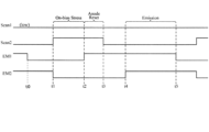
- FIG. 2 is a timing chart showing changes in the scanning control signals Scan1, Scan2 and the emission control signals EM1, EM2 given to this pixel circuit during the refresh frame period. Due to such signal changes, this pixel circuit operates as follows during the refresh frame period. The operation of this pixel circuit during the refresh frame period will be described below with reference to FIG.
- the transistor Tr5 changes from on to off to start a non-light-emitting period, which continues until time t5, which will be described later.
- the initialization period t1-t2 which is the period from time t1 to time t2 in the non-light-emitting period t1-t5
- the transistors Tr3, Tr4 and Tr6 are on, and the transistors Tr1 and Tr5 are off.
- the high-level power supply voltage VDDEL and the initialization voltage Vini are applied to one end (Node2) and the other end of the holding capacitor Cst, respectively, and the voltage VDDEL-Vini is held in the holding capacitor Cst at time t2.
- the transistors Tr3, Tr4, and Tr6 are turned off, and the transistor Tr1 is turned on.
- the transistors Tr3, Tr4, and Tr6 are kept off, and the voltage of the signal line that transmits the voltage Vdata is applied as the on-bias voltage Vob to the drive transistor Tr2 via the transistor Tr1. is applied to the source terminal (Node3) of .
- the voltage stress corresponding to the difference between the voltage at one end (Node2) of the holding capacitor Cst and the on-bias voltage Vob (the voltage applied to Node3 via the transistor Tr1) is applied to the drive transistor Tr2. is applied between the gate and source of
- the transistor Tr3 is turned on, so that the drive transistor Tr2 is diode-connected, and the voltage Vdata is applied to one end of the holding capacitor Cst via the transistor Tr1 and the diode-connected drive transistor Tr2.
- This state continues during the compensation/writing period t3-t4, which is the period from time t3 to time t4.
- the voltage Vdata+Vth-Vini is held in the holding capacitor Cst, and the gate-source voltage Vgs of the driving transistor Tr2 is equal to the threshold voltage Vth (>0) of the driving transistor Tr2.
- the transistors Tr1, Tr3, and Tr6 are turned off, and thereafter maintained off.
- the transistors T4 and T5 still remain off and remain off until time t5.
- the gate-source voltage Vgs of the drive transistor Tr2 is maintained equal to the threshold voltage Vth of the drive transistor Tr2 during the period from time t4 to time t5.
- the transistors Tr4 and Tr5 are turned on. After time t5, the transistors Tr4 and Tr5 are kept on, the transistors Tr1, Tr3 and Tr6 are kept off, and a current corresponding to the voltage held in the holding capacitor Cst flows through the organic EL element 304. , the organic EL element 304 emits light with a luminance corresponding to the current.
- FIG. 3 is a timing chart showing changes in the scanning control signals Scan1, Scan2 and the emission control signals EM1, EM2 given to this pixel circuit during the non-refresh frame period. Due to such signal changes, this pixel circuit operates as follows during the non-refresh frame period. The operation of this pixel circuit during a non-refresh frame period will be described below with reference to FIG.
- a non-light emitting period is provided in the non-refresh frame period as well as the refresh frame period.
- the non-light-emitting period starts when the transistor Tr5 changes from the ON state to the OFF state, and the non-light-emitting period continues until time t4, which will be described later.
- the on-bias period t1 to t2 which is the period from time t1 to time t2 in the non-light emitting period t0 to t4
- the transistors Tr3, Tr4, and Tr6 are kept off, and the voltage of the signal line transmitting the voltage Vdata is turned on.
- a bias voltage Vob is applied to the source terminal (Node3) of the driving transistor Tr2.
- the transistor Tr5 is turned on, and the voltage of the signal line transmitting the voltage Vdata is applied to the anode of the organic EL element 304 as the anode initialization voltage.
- the application of this anode initialization voltage to the anode of the organic EL element 304 continues until the transistor Tr1 turns off at time 3 . That is, the period from time 2 to time t3 is the anode initialization period.
- the transistor Tr1 is turned off, the transistors Tr3 and Tr4 are kept off, and the transistor Tr5 is kept on. After that, the transistors Tr1, Tr3, and Tr4 are off and the transistor Tr5 is on until time t5.
- the voltage held in the holding capacitor Cst is applied between the gate and source of the driving transistor Tr2, which acts as a voltage stress on the driving transistor Tr2.
- the transistor Tr4 is turned on, the transistor Tr5 is kept on, and the transistors Tr1, Tr3, and Tr6 are kept off.
- a current corresponding to the voltage held in the holding capacitor Cst flows through the organic EL element 304, and the organic EL element 304 emits light with a luminance corresponding to the current.
- This light emitting state continues until the transistor Tr5 turns off at time t5. That is, the light emission period is from time t4 to time t5.
- the voltage held in the holding capacitor Cst is applied between the gate and source of the driving transistor Tr2, and this acts as a voltage stress on the driving transistor Tr2.
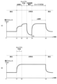
- FIG. 4 is a waveform diagram for explaining a problem caused by the hysteresis characteristic of the drive transistor in the pixel circuit shown in FIG. 1 when the light emission duty is low.
- 4A shows the voltage Vgs between the gate and source of the drive transistor Tr2 during the refresh frame period as the voltage stress applied to the drive transistor Tr2
- FIG. 4B shows the drive voltage Vgs during the non-refresh frame period.
- a voltage Vg between the gate and source of the transistor Tr2 is shown as voltage stress applied to the drive transistor Tr2.
- the scanning control signals Scan1 and Scan2 and the light emission control signals EM1 and EM2 change as shown in FIG. 2 to operate the pixel circuit of FIG.
- the applied voltage stress (Vgs) changes as shown in FIG. 4(A). That is, based on the above-described operation during the refresh frame period, the voltage held in the holding capacitor Cst is applied to the driving transistor Tr2 as voltage stress (Vgs) during the light emission period, and during the initialization period t1 to t2, the holding capacitor Cst A high-level power supply voltage VDDEL is applied to the gate terminal (Node2) of the drive transistor Tr2 for initialization of the drive transistor Tr2, thereby increasing the voltage stress (Vgs) applied to the drive transistor Tr2.
- the voltage of the signal line that transmits the voltage Vdata is applied as the on-bias voltage Vob to the source terminal (Node3) of the driving transistor Tr2 via the transistor Tr1.
- the applied voltage stress (Vgs) further increases.
- the voltage Vdata is written to the holding capacitor Cst via the diode-connected drive transistor Tr2, and the voltage stress (Vgs) applied to the drive transistor Tr2 is equal to the threshold voltage Vth of the drive transistor Tr2. equal to
- period A the period from time t4 to time t5
- the transistors Tr1 and Tr3 to Tr6 are in the off state, and the voltage stress (Vgs) applied to the driving transistor Tr2 is maintained at the threshold voltage Vth.
- the scanning control signals Scan1 and Scan2 and the emission control signals EM1 and EM2 change as shown in FIG. 3, thereby operating the pixel circuit of FIG.
- the voltage stress (Vgs) applied to the transistor Tr2 changes as shown in FIG. 4B. That is, based on the above-described operation during the refresh frame period, the voltage held in the holding capacitor Cst is applied to the drive transistor Tr2 as voltage stress (Vgs) during the light emission period.
- the voltage of the signal line that transmits the voltage Vdata is applied as the on-bias voltage Vob to the source terminal (Node3) of the driving transistor Tr2 via the transistor Tr1, thereby causing the driving transistor Tr2 to The applied voltage stress (Vgs) increases.
- the voltage stress applied to the driving transistor Tr2 in the non-light emitting period differs between the refresh frame period and the non-refresh frame period. That is, the voltage stress (Vgs) applied to the drive transistor Tr2 is relatively small and equal to the threshold voltage Vth during the A period within the refresh frame period, but during the period corresponding to the A period within the non-refresh frame period, the voltage stress (Vgs) applied to the holding capacitor Cst relatively large, equal to the voltage being held.
- the A period becomes longer, and as a result, the voltage stress applied to the drive transistor Tr2 greatly differs between the refresh frame period and the non-refresh frame period.
- flicker is visible even if the on-bias voltage is applied as described above in order to reduce the threshold shift due to the hysteresis characteristic of the drive transistor Tr2.
- the inventors of the present application have solved the above problem by "expanding the period A included in the refresh frame period so as to reduce the difference in the stress state of the driving transistor Tr2 between the refresh frame period and the non-refresh frame period.”
- the on-bias voltage is applied to the drive transistor Tr2 for at least part of the period from the end time t4 of the compensation/write period to the start time t5 of the next light emission period.
- Vgs voltage stress
- FIG. 5 is a waveform diagram for explaining this solution.
- FIG. 5A shows the voltage stress (gate-source voltage Vgs) applied to the driving transistor Tr2 during the refresh frame period in the display device to which this solution is applied
- FIG. It shows the voltage stress (gate-source voltage Vgs) applied to the drive transistor Tr2 during the non-refresh frame period in the display device.
- the pixel circuit is configured such that the voltage stress (Vgs) given to the drive transistor Tr2 by the application of the on-bias voltage Vob during the non-light emitting period within the non-refresh period is maintained until the start time t4 of the light emitting period. I assumed there was. Therefore, the waveform diagram of FIG. 5B is different from the waveform diagram of FIG. 4B.
- the gate terminal corresponds to the control terminal
- one of the drain terminal and the source terminal corresponds to the first conduction terminal
- the other corresponds to the second conduction terminal.
- connection in this specification means “electrical connection” unless otherwise specified. Indirect connection via an element is also included.
- FIG. 6 is a block diagram showing the overall configuration of the display device 10 according to the first embodiment.
- This display device 10 is an organic EL display device that performs internal compensation. That is, in the display device 10, each pixel circuit has a function of compensating for variations and fluctuations in the threshold voltage of the driving transistor therein.
- the display device 10 also has two operation modes, a normal drive mode and a rest drive mode. That is, in the normal drive mode, the display device 10 operates so that the refresh frame periods Trf for rewriting the image data (data voltage in each pixel circuit) of the display section are continuous.
- a drive period TD and a pause period TP consisting of a plurality of non-refresh frame periods Tnrf for stopping rewriting of image data on the display section alternately appear (see FIG. 8 described later).
- the display device 10 includes a display section 11, a display control circuit 20, a data side drive circuit 30, a scanning side drive circuit 40, and a power supply circuit 50.
- the data side driver circuit 30 functions as a data signal line driver circuit (also called “data driver”).
- the scanning-side driving circuit 40 functions as a scanning signal line driving circuit (also called “gate driver”), a light emission control circuit (also called “emission driver”), and a bias control circuit.
- these three scanning-side circuits are realized as one scanning-side drive circuit 40, but these three circuits may be appropriately separated, and these three circuits may be separated. may be arranged separately on one side and the other side of the display section 11 .
- the power supply circuit 50 supplies the display unit 11 with a high-level power supply voltage ELVDD, a low-level power supply voltage ELVSS, an initialization voltage Vini, a display control circuit 20 , a data-side drive circuit 30 , and a scanning-side drive circuit 40 . and a power supply voltage (not shown) to be supplied to .
- the display unit 11 has m data signal lines D1, D2, .
- This (n is an integer equal to or greater than 2) second scanning signal lines NS-1, NS0, NS1, . . . , NSn are arranged.
- n light emission control lines (emission lines) EM1 to EMn are arranged along the n first scanning signal lines PS1 to PSn, respectively, and the n first scanning signal lines PS1 to PSn are provided with n light emission control lines (emission lines) EM1 to EMn, respectively.
- bias control lines n scanning signal lines for bias control
- the display unit 11 is provided with m ⁇ n pixel circuits 15 arranged in a matrix along m data signal lines D1 to Dm and n first scanning signal lines PS1 to PSn. .
- Each pixel circuit 15 corresponds to one of the m data signal lines D1 to Dm and corresponds to one of the n first scanning signal lines PS1 to PSn (hereinafter each pixel circuit 15 , the pixel circuit corresponding to the i-th first scanning signal line PSi and the j-th data signal line Dj is also referred to as the "i-th row j-th column pixel circuit", and the code "Pix (i, j )”).
- Each pixel circuit 15 corresponds to any one of the n second scanning signal lines NS1 to NSn and to any one of the n emission control lines EM1 to EMn. Each pixel circuit 15 also corresponds to any one of the n bias control lines PSB1 to PSBn. , Dm, the first scanning signal lines PS1, PS2, . . . , PSn, the second scanning signal lines NS-1, NS0, . , NSn, the emission control lines EM1 to EMn, and the bias control lines PSB1 to PSBn. configure (see FIG. 6).
- a power supply line (not shown) common to each pixel circuit 15 is arranged. That is, a first power supply line for supplying a high-level power supply voltage ELVDD for driving an organic EL element to be described later (hereinafter referred to as a "high-level power supply line” and indicated by the symbol “ELVDD” like the high-level power supply voltage). , and a second power supply line for supplying a low-level power supply voltage ELVSS for driving the organic EL element (hereinafter referred to as a "low-level power supply line” and indicated by the symbol “ELVSS” like the low-level power supply voltage). are arranged.
- the display unit 11 is provided with an initialization voltage line (not shown) for supplying an initialization voltage Vini used for a reset operation (also referred to as an “initialization operation”) for initializing each pixel circuit 15 . (indicated by the same symbol "Vini”) is also provided.
- a high-level power supply voltage ELVDD, a low-level power supply voltage ELVSS, and an initialization voltage Vini are supplied from the power supply circuit 50 .
- the display control circuit 20 receives an input signal Sin including image information representing an image to be displayed and timing control information for image display from the outside of the display device 10, and based on this input signal Sin, a data side control signal Scd and a scanning signal. A side control signal Scs is generated, and a data side control signal Scd and a scanning side control signal Scs are output to the data side driving circuit 30 and the scanning side driving circuit 40, respectively.
- the data side drive circuit 30 drives the data signal lines D1 to Dm based on the data side control signal Scd from the display control circuit 20. That is, the data-side drive circuit 30 generates m data signals D(1) to D(m) representing images to be displayed based on the data-side control signal Scd, and applies them to the data signal lines D1 to Dm, respectively. .
- the scanning drive circuit 40 drives the n first scanning signal lines PS1 to PSn and the n+2 second scanning signal lines NS-1 to NSn based on the scanning control signal Scs from the display control circuit 20. It functions as a signal line drive circuit, an emission control circuit that drives the emission control lines EM1 to EMn, and a bias control circuit that drives the bias control lines PSB1 to PSBn.
- the scanning-side driving circuit 40 drives the n first scanning signal lines PS1 to PSn for one horizontal period based on the scanning-side control signal Scs.
- n+2 second scanning signal lines NS-1 to NSn are sequentially selected for each predetermined period corresponding to one horizontal period, and the selected first scanning signal line PSk is activated.
- active signal (k is an integer satisfying 1 ⁇ k ⁇ n)
- an active signal is applied to the selected second scanning signal line NSs (s is an integer satisfying -1 ⁇ s ⁇ n)
- An inactive signal is applied to the unselected first scanning signal lines, and an inactive signal is applied to the unselected second scanning signal lines.
- m pixel circuits Pix(k, 1) to Pix(k, m) corresponding to the selected first scanning signal line PSk are collectively selected.
- m data signals D (1 ) to D(m) (hereinbelow, these voltages may be simply referred to as “data voltages” without distinction) are used as pixel data for the pixel circuits Pix(k, 1) to Pix(k, m ), respectively.
- N-type N-channel type
- a light-emission control signal high level
- a light emission control signal low level voltage
- the organic EL elements in the pixel circuits Pix (i, 1) to Pix (i, m) corresponding to the i-th first scanning signal line PSi are connected to the light emission control line. While the voltage of EMi is at the low level (activated state), the i-th pixel circuits Pix(i, 1) to Pix(i, m) emit light with luminance corresponding to the data voltages written respectively. Note that the scanning-side drive circuit 40 drives the emission control lines EM1 to EMn in the non-refresh frame period Tnrf in the same manner as in the refresh frame period Trf (see FIG. 8 described later).
- the scanning-side drive circuit 40 drives the bias control lines PSB1 to PSBn so that they are sequentially selected in both the refresh frame period Trf and the non-refresh frame period Tnrf in the rest drive mode. (See FIG. 8, which will be described later). Details of this operation will be described later.
- driving of the bias control lines PSB1-PSBn is stopped, and the bias control lines PSB1-PSBn are all maintained in an inactive state.
- the display device 10 has two operation modes, the normal drive mode and the pause drive mode. First, the general operation of the display device 10 in the normal drive mode will be described.
- FIG. 7 is a timing chart for explaining the schematic operation of the display device 10 in normal drive mode.
- the scanning-side control signal Scs supplied from the display control circuit 20 to the scanning-side driving circuit 40 includes a two-phase clock signal composed of the first and second gate clock signals CK1 and CK2.
- the scan-side drive circuit 40 In the normal drive mode, the scan-side drive circuit 40 generates first scan signals PS(1) to PS(n) and second scan signals NS(-1), NS as shown in FIG. 7 based on the two-phase clock signals. (0), NS(1), . NS(-1) to NS(n) are applied to the second scanning signal lines NS-1 to NSn, respectively. Further, the scanning-side drive circuit 40 generates emission control signals EM(1) to EM(n) as shown in FIG.
- the data-side drive circuit 30 Based on the data-side control signal Scd from the display control circuit 20, the data-side drive circuit 30 outputs a data signal that changes in conjunction with the first scanning signals PS(1) to PS(n) as shown in FIG. D(1) to D(m) are generated and applied to the data signal lines D1 to Dm, respectively.
- each pixel circuit Pix(i, j) is initialized and data voltage is written. to emit light.
- the above various signals shown in FIG. By being driven as described above, the first scanning signal lines NS-1 to NSn and the second scanning signal lines PS1 to PSn are sequentially selected in one frame period, and the pixel circuits Pix (1, 1 of the display section 11) are selected. ) to Pix(n,m)) are repeated.
- RF frame period refresh frame period
- NRF frame periods non-refresh frame periods
- the scanning side driving circuit 40 drives the first scanning signal lines PS1 to PSn and the second scanning signal lines NS-1 to NSn, and the data side driving circuit 30 drives the data signal lines D1 to
- the driving of Dm is stopped, and the display based on the image data written in the previous driving period TD (RF frame period Trf) continues. Therefore, the rest drive mode is effective in reducing the power consumption of the display device 10 when displaying a still image.
- the first scanning signal lines PS1 to PSn are driven even during the pause period TP.
- Bias control lines PSB1-PSBn are driven so as to be sequentially selected in both RF frame period Trf and NRF frame period Tnrf in the rest drive mode as shown in FIG.
- the on-bias voltage is applied to the drive transistor while the corresponding bias control line PSBi is in the activated state (details are later).
- the drive period TD consists of only one RF frame period Trf in the example shown in FIG. 8, it may consist of two or more RF frame periods Trf.
- the input signal Sin from the outside includes an operation mode signal Sm that indicates in which operation mode the display unit 11 is to be driven, the normal drive mode or the rest drive mode.
- This operation mode signal Sm is applied to the scanning side driving circuit 40 as part of the scanning side control signal Scs, and is also applied to the data side driving circuit 30 as part of the data side control signal Scd.
- the scanning-side drive circuit 40 drives the first scanning signal lines PS1 to PSn and the second scanning signal lines NS-1 to NSn according to the operation mode indicated by the operation mode signal Sm, and drives the emission control lines EM1 to EMn. They are driven in the same form (same period and same duty) regardless of whether they are in the normal drive mode or the rest drive mode.
- the scanning side drive circuit 40 drives the bias control lines PSB1 to PSBn in the pause drive mode, and stops driving them in the normal drive mode.
- the data side drive circuit 30 drives the data signal lines D1 to Dn according to the operation mode indicated by this operation mode signal Sm. Since the subject of the present application is not related to the normal drive mode, the operation of the display device 10 or its pixel circuit will be mainly described below in the rest drive mode (the same applies to other embodiments described later). .
- each pixel circuit Pix(i, j) data is written when the corresponding first and second scanning signal lines PSi, NSi are in the selected state.
- An initializing operation is performed when the second scanning signal line NSi-2 two lines before the second scanning signal line NSi is in a selected state.
- each emission control line EMi is at a low level.
- a (L level) voltage is applied, it is activated, and when a high level (H level) voltage is applied, it is deactivated.
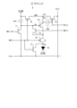
- FIG. 9 is a circuit diagram showing the configuration of the pixel circuit 15 in this embodiment.
- FIG. 4 is a circuit diagram showing a configuration of a j-th pixel circuit Pix(i,j) (1 ⁇ i ⁇ n, 1 ⁇ j ⁇ m);
- the pixel circuit 15 includes one organic EL element OL as a display element and seven transistors T1 to T7 (hereinafter referred to as "first initialization transistor T1", “threshold compensation transistor T2", “writing transistor T2").
- a control transistor T3, a drive transistor T4 a first emission control transistor T5, a second emission control transistor T6, and a second initialization transistor T7, and one holding capacitor Cst. I'm in.
- the pixel circuit 15 also includes a bias applying circuit 151 including a transistor T8 (hereinafter, this transistor T8 is referred to as a "bias applying transistor”).
- transistors T1, T2, and T7 are N-type transistors, and transistors T3 to T6 are P-type transistors.
- the N-type transistors T1, T2, and T7 are thin film transistors (hereinafter referred to as “oxide TFTs”) whose channel layers are made of an oxide semiconductor.
- oxide TFTs This is an oxide TFT (hereinafter referred to as “IGZO-TFT”) using InGaZnO). Since the oxide TFT has a small off-leak current, it is suitable as a switching element in a pixel circuit or the like.
- the P-type transistors T3 to T6 are thin film transistors (hereinafter referred to as "LTPS-TFT") whose channel layers are made of low-temperature polysilicon. Since low-temperature polysilicon has high mobility, the use of LTPS-TFTs as drive transistors improves the drive capability for organic EL elements in pixel circuits, and the use of LTPS-TFTs as switching elements reduces the on-resistance.
- transistors that can be used in the pixel circuit 15 are not limited to such IGZO-TFTs and LTPS-TFTs.
- the transistors T1 to T3 and T5 to T8 other than the driving transistor T4 operate as switching elements.
- the holding capacitor Cst is a capacitive element having two electrodes consisting of a first electrode and a second electrode.
- the pixel circuit Pix(i, j) in the present embodiment includes a corresponding first scanning signal line (hereinafter referred to as a "corresponding first scanning signal line” in the description focusing on the pixel circuit).
- PSi a corresponding second scanning signal line
- NSi a corresponding bias control line
- EMi a corresponding emission control line
- EMi a corresponding emission control line
- corresponding data signal line (hereinafter also referred to as "corresponding data signal line” in the description focused on the pixel circuit) Dj and second scanning signal lines (second scanning signal lines NS-1 to NSn), that is, the i-2-th second scanning signal line NSi-2 (hereinafter also simply referred to as the "previous second scanning signal line” in the description focused on the pixel circuit).
- second scanning signal lines NS-1 to NSn that is, the i-2-th second scanning signal line NSi-2 (hereinafter also simply referred to as the "previous second scanning signal line” in the description focused on the pixel circuit).
- an initialization voltage line Vini an on-bias voltage line Lobs
- ELVDD high-level power supply line
- ELVSS low-level power supply line
- the pixel circuit Pix(i,j) may be connected to the preceding second scanning signal line NSi-1 instead of the preceding second scanning signal line NSi-2.
- the signal PS(i) of the corresponding first scanning signal line PSi, the signal NS(i) of the corresponding second scanning signal line NSi, the signal NS(i-2) of the preceding second scanning signal line NSi-2, the corresponding The signal EM(i) on the emission control line EMi, the signal PSB(i) on the corresponding bias control line PSBi, and the signal D(j) on the corresponding data signal line Dj are converted into corresponding first scanning signals PS(i), a corresponding second scanning signal NS(i), a preceding second scanning signal NS(i-2), a corresponding emission control signal EM(i), a corresponding bias control signal PSB(i), and a corresponding data signal D(j); shall be called.
- the on-bias voltage lines Lobs which are not shown in FIG. 3, may be arranged along the data signal lines D1 to Dm, for example, so that the on-bias voltage Vobs can be applied from the data side drive circuit 30. .
- the on-bias voltage Vobs is set according to the display gradation, refresh rate, environmental temperature, on-bias application period (the length of the period during which the on-bias voltage Vobs is applied), and the like. For example, representative values such as the average value, median value, and mode of one or more of these operating condition parameters (including light emission duty) are obtained in advance by statistical processing, and the display device
- An appropriate on-bias voltage Vobs may be determined as a fixed value for each ten solids or each product. Alternatively, an appropriate on-bias voltage Vob may be set as a variable value based on one or more values of these operating condition parameters.
- the source terminal of the drive transistor T4 is connected to the corresponding data signal line Dj through the write control transistor T3, and is connected to the first emission control transistor T5. , to the high-level power supply line ELVDD.
- the drain terminal of the driving transistor T4 is connected to the anode serving as the first terminal of the organic EL element OL through the second emission control transistor T6, and the cathode of the organic EL element OL is connected to the low level power supply line ELVSS.
- the gate terminal of the drive transistor T4 is connected to the drain terminal of the drive transistor T4 through the threshold compensation transistor T2, is connected to the high level power supply line ELVDD through the holding capacitor Cst, and is connected to the first initialization transistor T1. , to the initialization voltage line Vini.
- the anode of the organic EL element OL is also connected to the initialization voltage line Vini through a second initialization transistor T7 as a display element initialization transistor.
- the bias application circuit 151 has a first terminal connected to the on-bias voltage line Lobs to receive the on-bias voltage, and a second terminal connected to the source terminal of the drive transistor T4. includes a biasing transistor T8 having source and drain terminals respectively connected to . The gate terminal of this bias applying transistor T8 is connected to the corresponding bias control line PSBi.
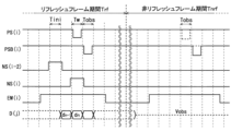
- FIG. 10 is a timing chart for explaining the operation of the pixel circuit Pix(i,j) in the non-light emitting period included in the refresh frame period (RF frame period) Trf and the non-refresh frame period (NRF frame period) Tnrf. be.
- FIG. 10 shows a plurality of dotted lines extending in the vertical direction, and the interval between these dotted lines corresponds to one horizontal period.
- the period during which the light emission control signal EM(i) is at H level is the non-light emission period, and the period during which the light emission control signal EM(i) is at L level is the light emission period (these points are shown in the timing charts to be described later). The same applies to FIGS. 12, 14, etc.).
- the operation of the pixel circuit Pix(i, j) during the non-light emitting period in the RF frame period Trf will be described.
- the corresponding first scanning signal PS(i) and the corresponding bias control signal PSB(i) are is H level
- the preceding second scanning signal NS(i-2) and the corresponding second scanning signal NS(i) are at L level.
- the organic EL element OL is extinguished because the first and second light emission control transistors T5 and T6 are off, and the second initialization transistor T7 is on so that the organic EL element OL is turned on. are initialized.
- the preceding second scanning signal NS(i-2) is at the H level for a predetermined period corresponding to approximately one horizontal period, and the corresponding bias control signal is maintained during this predetermined period.
- PSB(i) is at L level for a predetermined period corresponding to approximately one horizontal period.
- the horizontal period during which the preceding second scanning signal NS(i-2) is at H level and the corresponding bias control signal PSB(i) is at L level is called "initializing period Tini".
- the first initialization transistor T1 is in the ON state, so that the voltage of the holding capacitor Cst and the gate terminal of the drive transistor T4 (hereinafter referred to as "gate voltage") is initialized to the initialization voltage Vini. .
- the on-bias voltage Vobs is applied from the on-bias voltage line Lobs to the source terminal of the driving transistor T4 by turning on the bias applying transistor T8 (see FIG. 9). Therefore, this initialization period Tini is also the on-bias application period Tobs.
- the corresponding second scanning signal NS(i) is at the H level for a predetermined period corresponding to approximately one horizontal period, and within this predetermined period, the corresponding first scanning signal PS(i) is at approximately one horizontal period. It is at L level only for a predetermined period corresponding to the period.
- the horizontal period during which the corresponding second scanning signal NS(i) is at H level and the corresponding first scanning signal PS(i) is at L level is called "compensation/writing period Tw" or simply "writing period Tw".
- the drive transistor T4 is diode-connected by turning on the threshold compensating transistor T2, and the corresponding data signal D(j) is turned on by turning on the write control transistor T3. is written to the holding capacitor Cst through the diode-connected drive transistor T4.
- the gate terminal of the drive transistor T4 is held at the data voltage (Vdata-
- Vth is the threshold voltage of the driving transistor T4.
- the corresponding bias control signal PSB(i) again becomes H level for a predetermined period corresponding to approximately one horizontal period.
- the corresponding second scanning signal NS(i) is maintained at L level.
- the horizontal period during which the corresponding bias control signal PSB(i) is at L level is also referred to as the "on-bias application period Tobs".
- the on-bias voltage Vobs is applied from the on-bias voltage line Lobs to the source terminal of the drive transistor T4 via the on-state bias application transistor T8 (see FIG. 9).
- the threshold compensating transistor T2 is in the off state after the writing period Tw, and is maintained in the off state also during the on-bias application period Tobs.
- the corresponding light emission control signal EM(i) changes to L level, thereby starting the light emission period.
- the first and second light emission control transistors T5 and T6 are on, and the transistors T1, T2, T3, T7 and T8 other than the drive transistor T4 are off.
- a current I1 corresponding to the data voltage Vdata written to the holding capacitor Cst flows through the organic EL element OL, and the organic EL element OL emits light with a luminance corresponding to the current I1.
- the on-bias voltage Vobs is applied to the source terminal of the drive transistor T4.
- the waveform representing the voltage stress (Vgs) applied to the drive transistor T4 during the RF frame period Trf becomes similar to the waveform shown in FIG. 5A.
- the operation of the pixel circuit Pix(i,j) during the non-light emitting period in the NRF frame period Tnrf will be described.
- the corresponding first scanning signal PS(i) and the corresponding bias control signal PSB(i) are at the H level, as in the case of the RF frame period Trf.
- the preceding second scanning signal NS(i-2) and the corresponding second scanning signal NS(i) are at L level.
- the corresponding bias control signal PSB(i) when this non-emission period starts (when the corresponding emission control signal EM(i) changes to H level), the corresponding bias control signal PSB(i) is set at a predetermined level corresponding to approximately one horizontal period.
- the ON-bias voltage Vobs is applied from the ON-bias voltage line Lobs to the source terminal of the driving transistor T4 by the L level only for the period and the bias-applying transistor T8 being turned ON.
- the horizontal period during which the corresponding bias control signal PSB(i) is at L level is also referred to as the "on-bias application period Tobs".
- the first initialization transistor T1, the threshold compensation transistor T2, and the write control transistor T3 are kept off during the NRF frame period Tnrf (see FIGS. 9 and 10).
- Data signals D(1)-D(m) applied to data signal lines D1-Dm are all maintained in a high impedance state.
- the corresponding light emission control signal EM(i) changes to L level and the light emission period starts.
- the pixel circuit Pix(i,j) operates in the same manner as during the light emission period during the RF frame period Trf. That is, a current I1 corresponding to the data voltage Vdata written to the holding capacitor Cst in the immediately preceding RF frame period Trf flows through the organic EL element OL, and the organic EL element OL emits light with a luminance corresponding to the current I1.
- the on-bias voltage Vobs is applied to the source of the drive transistor T4 in the on-bias application period Tobs. applied to the terminal.
- a relatively large voltage stress (Vgs) is applied to the drive transistor T4 until the start of the light emission period, and the voltage stress (Vgs) applied to the drive transistor T4 during the NRF frame period Tnrf is reduced to
- the waveform shown is substantially the same as the waveform shown in 4(B) and FIG. 5(B).
- each pixel circuit Pix(i, j) is shown in FIG. , in both the RF frame period Trf (within the drive period TD) and the NRF frame period Tnrf (within the idle period TP), the light is periodically turned off by driving the light emission control signal EM(i), and the light is turned off.
- An on-bias voltage is applied to the drive transistor T4 during the period (non-emission period).
- an on-bias application period Tobs is provided not only before the compensation/write period Tw but also after the compensation/write period Tw, for threshold compensation during writing of the data voltage Vdata.
- the on-bias voltage Vobs is applied to the driving transistor T4 also after the period in which the threshold compensating transistor T2 is turned on.
- Vgs voltage stress
- the waveform representing the voltage stress (Vgs) applied to the driving transistor T4 in the RF frame period Trf is close to the waveform shown in FIG. 5A.
- the waveform representing the voltage stress (Vgs) applied to the drive transistor T4 in the NRF frame period Tnrf is substantially the same as the waveform shown in FIG. 5B.
- the difference in the stress state of the driving transistor T4 between the refresh frame period Trf and the non-refresh frame period Tnrf is reduced (( A) and (B)).
- the difference in brightness between the refresh frame period Trf and the non-refresh frame period Tnrf is reduced, and flicker is not visible even if the light emission duty is set low and rest driving is performed. That is, according to the present embodiment, a flicker suppression effect that does not depend on the light emission duty can be obtained when the pause drive is performed.
- the period during which the voltage stress (Vgs) to the driving transistor T4 is small (Vth) during data writing is about one horizontal period, which is relatively short. , the decrease in the stress voltage (Vgs) during this period does not pose a problem in the flicker suppression described above.
- FIG. 11 an organic EL display device according to a second embodiment will be described with reference to FIGS. 11 and 12.
- FIG. the bias control lines PSB1 to PSBn are provided as in the display device according to the first embodiment, but the on-bias voltage line Lobs is not provided, and the voltage of the first scanning signal line is used as the on-bias voltage Vobs.
- the pixel circuit in this embodiment is provided with a bias applying circuit, like the pixel circuit in the first embodiment. However, its configuration is slightly different from the configuration of the bias application circuit in the first embodiment.
- Other configurations of the display device according to the present embodiment are basically the same as those of the display device according to the first embodiment. Description is omitted (see FIG. 6).
- FIG. 11 is a circuit diagram showing the configuration of the pixel circuit 15 in this embodiment.
- FIG. 4 is a circuit diagram showing a configuration of a j-th pixel circuit Pix(i,j) (1 ⁇ i ⁇ n, 1 ⁇ j ⁇ m);
- This pixel circuit 15 has the same configuration as the pixel circuit 15 (FIG. 9) in the first embodiment, except for the configuration of the bias application circuit 151 . Therefore, in the configuration of the pixel circuit 15, the components other than the bias applying circuit 151 are the same as those of the pixel circuit 15 in the first embodiment, and the same reference numerals are given to the same components, and a detailed description thereof will be given. omitted.
- the pixel circuit Pix(i, j) of the i-th row, j-th column which is the pixel circuit 15 in this embodiment, has a corresponding first scanning signal line PSi, a corresponding bias control line PSBi, and a corresponding second scanning signal line PSi.
- a scanning signal line NSi, a preceding second scanning signal line NSi-2, a corresponding emission control line EMi, a corresponding data signal line Dj, an initialization voltage line Vini, a high level power supply line ELVDD, and a low level power supply line ELVSS are connected.
- the bias application circuit 151 provided in the pixel circuit 15 is connected to the corresponding first scanning signal line PSi and receives the voltage of the corresponding first scanning signal PS(i) in the inactive state as the on-bias voltage Vobs. It includes a biasing transistor T8 having one terminal and a second terminal connected to the source terminal of the drive transistor T4 and having source and drain terminals connected to the first and second terminals, respectively.
- the bias applying transistor T8 has a gate terminal connected to the corresponding bias control line PSBi and operates as a switching element.
- FIG. 12 is a timing chart for explaining the operation of the pixel circuit Pix(i,j) during the non-light emitting period included in the RF frame period Trf and the NRF frame period Tnrf.
- the first scanning signal PS (i ), second scanning signals NS(i), NS(i ⁇ 2), emission control signal EM(i), and data signal D(j) are the pixel circuits Pix(i, j ), second scanning signals NS(i) and NS(i ⁇ 2), emission control signal EM(i), and data signal D(j) for driving Change.
- the transistors T1 to T3 and T5 to T7 serving as switching elements included in the pixel circuit 15 of the present embodiment are replaced with the transistors T1 to T3 and T5 serving as switching elements included in the pixel circuit 15 of the first embodiment.
- the same initialization operation and data write operation are performed.
- a data write operation is performed via the diode-connected drive transistor T4 to perform threshold compensation.
- the corresponding bias control signal PSB(i) is maintained at H level (inactive) during the initialization period Tini, and is maintained at H level (inactive) for a predetermined period during the horizontal period immediately after the compensation/write period Tw. only becomes L level (active).
- the horizontal period during which the corresponding bias control signal PSB(i) is at L level is called "on-bias application period Tobs".
- the bias control lines PSB1 to PSBn are driven so as to be sequentially selected in both the RF frame period Trf and the NRF frame period Tnrf in the rest drive mode as shown in FIG.
- the first scanning signal PS(i) corresponding to the drive transistor T4 is applied. is applied as the on-bias voltage Vobs. Since the corresponding first scanning signal PS(i) is in the non-selected state during the on-bias application period Tobs, the H-level voltage of the corresponding first scanning signal PS(i) is applied as the on-bias voltage Vobs to the source terminal of the drive transistor T4.
- a relatively large voltage stress (Vgs) is applied to the drive transistor T4 from the application of this on-bias voltage Vobs to the start of the light emission period.
- the period during which this relatively large voltage stress (Vgs) is applied to the driving transistor T4 becomes longer as the light emission duty becomes lower.
- the position and length of the period during which such a relatively large voltage stress (Vgs) is applied to the driving transistor T4 is the same in the NRF frame period Tnrf.
- the difference in the stress state of the drive transistor T4 between the RF frame period Trf and the NRF frame period Tnrf is reduced.
- the luminance difference between the refresh frame period Trf and the non-refresh frame period Tnrf is also reduced, and flicker is not visually recognized even if the light emission duty is set low and rest driving is performed. That is, according to the present embodiment, a flicker suppression effect that does not depend on the light emission duty can be obtained when the pause drive is performed.
- the bias control lines PSB1 to PSBn may be maintained in an inactive state during the NRF frame period Tnrf (in FIG. 12, the first scanning signal PS(i) and the bias control signal PSB(i) (Refer to the part indicated by the dotted line for the waveform of ).
- the corresponding bias control line PSBi is connected to the gate terminal of the bias applying transistor T8 constituting the bias applying circuit 151, and the corresponding bias control signal PSB(i) On/off of the bias applying transistor T8 is controlled.
- the first scanning signal line PSi+1 immediately after the corresponding first scanning signal line PSi may be connected to the gate terminal of the bias applying transistor T8.
- the corresponding first scanning signal line PSi is connected to the first terminal of the bias applying circuit 151, and when the corresponding first scanning signal PS(i) is H level voltage is applied to the bias application circuit 151 as the on-bias voltage Vobs.
- another signal line may be connected to the first terminal.
- the corresponding emission control line EMi or the second scanning signal line NSi+1 immediately after the corresponding second scanning signal line NSi is connected to the first terminal of the bias applying circuit 151. may be connected.
- the corresponding bias control signal PSB(i) for controlling the ON/OFF of the bias applying transistor T8 in each pixel circuit P(i, j) changes as shown in FIG. 10
- the corresponding bias control signal PSB(i) may change as shown in FIG.
- the corresponding bias control signal PSB(i) in the RF frame period Trf, not only becomes L level after the compensation/writing period Tw, but also becomes L level during the initialization period Tini.
- the H level voltage of (i) is applied to the source terminal of the driving transistor T4 as the on-bias voltage Vobs.
- FIG. 13 to 15 An organic EL display device according to a third embodiment will be described with reference to FIGS. 13 to 15.
- FIG. In this display device, none of the bias control lines PSB1 to PSBn and the bias voltage line Lobs in the display device according to the first embodiment are provided, and the voltage of the second scanning signal line is used as the on-bias voltage Vobs. be done.
- the pixel circuit of the present embodiment is provided with a bias application circuit like the pixel circuit of the first embodiment, but the configuration thereof is different from that of the bias application circuit of the first embodiment. do.
- Other configurations of the display device according to the present embodiment are basically the same as those of the display device according to the first embodiment. Description is omitted (see FIG. 6).
- FIG. 13 is a circuit diagram showing the first configuration of the pixel circuit 15 in this embodiment.
- FIG. 3 is a circuit diagram showing a configuration of a pixel circuit Pix(i, j) in the i-th row and the j-th column (1 ⁇ i ⁇ n, 1 ⁇ j ⁇ m);
- This pixel circuit 15 has the same configuration as the pixel circuit 15 (FIG. 9) in the first embodiment, except for the configuration of the bias application circuit 151 . Therefore, in the configuration of the pixel circuit 15, the components other than the bias applying circuit 151 are the same as those of the pixel circuit 15 in the first embodiment, and the same reference numerals are given to the same components, and a detailed description thereof will be given. omitted.
- the pixel circuit Pix(i, j) of the i-th row and the j-th column which is the pixel circuit 15 in this embodiment, includes the corresponding first scanning signal line PSi, the corresponding second scanning signal line NSi, the preceding A second scanning signal line NSi-2, a corresponding emission control line EMi, a corresponding data signal line Dj, an initialization voltage line Vini, a high level power supply line ELVDD, and a low level power supply line ELVSS are connected.
- a second scanning signal line NSi+X is connected.
- X is a positive integer
- the period during which the second scanning signal NS(i+X) of the subsequent second scanning signal line is at H level is the non-light emitting period in the pixel circuit Pix(i, j). selected to be included (see FIG. 14 below).
- the subsequent second scanning signal line NSi+X specified by X is simply referred to as "subsequent second scanning signal line NSi+X”.
- the signal on the subsequent second scanning signal line NSi+X is referred to as "subsequent second scanning signal NS(i+X)" ( The same applies to other embodiments described later).
- the bias application circuit 151 provided in the pixel circuit 15 is connected to the subsequent second scanning signal line NSi+X to turn on the voltage of the subsequent second scanning signal NS(i+X).
- a P-type transistor having a first terminal for receiving a bias voltage Vobs, a second terminal connected to the source terminal of the drive transistor T4, and having source and drain terminals connected to the first and second terminals, respectively. It includes a biasing transistor T8.
- the bias applying transistor T8 is diode-connected with its gate terminal connected to its drain terminal.
- FIG. 14 is a timing chart for explaining the operation of the pixel circuit Pix(i,j) during the non-light emitting period included in the RF frame period Trf and the NRF frame period Tnrf.
- the first scanning signal PS (i ), second scanning signals NS(i), NS(i ⁇ 2), emission control signal EM(i), and data signal D(j) are the pixel circuits Pix(i, j ), second scanning signals NS(i) and NS(i ⁇ 2), emission control signal EM(i), and data signal D(j) for driving Change.
- the transistors T1 to T3 and T5 to T7 serving as switching elements included in the pixel circuit 15 of the present embodiment are replaced with the transistors T1 to T3 and T5 serving as switching elements included in the pixel circuit 15 of the first embodiment.
- threshold value compensation is performed by performing a data write operation through the diode-connected drive transistor T4.
- the bias applying circuit 151 receives the subsequent second scanning signal NS(i+X) at its first terminal.
- This first terminal is connected to the source terminal of the driving transistor T4 via the bias applying transistor T8 in a diode-connected state as shown in FIG. Therefore, when the subsequent second scanning signal NS(i+X) is at H level, the H level voltage is applied to the source terminal of the driving transistor T4 via the bias applying transistor T8.
- the subsequent second scanning signal NS(i+X) is at H level.
- the certain period is included between the end of the compensation/write period Tw and the start of the light emission period. Therefore, in the present embodiment, this period is the on-bias application period Tobs, and during this on-bias application period Tobs, the H-level voltage of the subsequent second scanning signal NS(i+X) serves as the on-bias voltage Vobs, and the driving transistor T4.
- a relatively large voltage stress (Vgs) is applied to the drive transistor T4 from the application of the on-bias voltage Vobs to the start of the light emission period.
- the period during which a relatively large voltage stress (Vgs) is applied to the drive transistor T4 in the RF frame period Trf in this way does not depend on the light emission duty at the start time, similar to the period during the NRF frame period Tnrf described later. The length becomes longer as the light emission duty becomes lower.
- the first scanning signal lines PS1 to PSn are also sequentially selected in the same manner during both the RF frame period Trf and the NRF frame period Tnrf. is driven to
- the on-bias application period Tobs for applying the on-bias voltage Vobs is provided between the end of the compensation/write period Tw and the start of the light emission period in the RF frame period Trf. Therefore, the difference in the stress state of the drive transistor T4 between the RF frame period Trf and the NRF frame period Tnrf is reduced. As a result, the same effects as those of the first and second embodiments can be obtained in this embodiment as well.
- FIG. 15 is a circuit diagram showing the second configuration of the pixel circuit 15 in this embodiment.
- FIG. 3 is a circuit diagram showing a configuration of a pixel circuit Pix(i, j) in the i-th row and the j-th column (1 ⁇ i ⁇ n, 1 ⁇ j ⁇ m);
- This pixel circuit 15 differs from the pixel circuit 15 (FIG. 13) according to the first configuration example in that the bias application transistor T8 in the bias application circuit 151 is of N type, but the other configurations are the same as those of the first configuration example. are the same.
- the bias application circuit 151 in this configuration example also has a first terminal that receives the voltage of the subsequent second scanning signal NS(i+X) as the on-bias voltage Vobs, and a second terminal that is connected to the source terminal of the drive transistor T4. there is A drain terminal and a source terminal of a bias applying transistor T8 are connected to these first and second terminals, respectively.
- the bias applying transistor T8 has its gate terminal connected to its drain terminal to form a diode connection. ing.
- the pixel circuit Pix(i, j) In the pixel circuit Pix(i, j) according to this configuration example, the first scanning signal PS(i), the second scanning signals NS(i), NS(i ⁇ 2), NS(i+2) that change as shown in FIG. ), the light emission control signal EM(i), and the data signal D(j), the pixel circuit Pix(i,j) operates in the same manner as the pixel circuit Pix(i,j) according to the first configuration example. Therefore, even when the pixel circuit Pix(i, j) according to the present configuration example is used in the present embodiment, the same effect as when the pixel circuit Pix(i, j) according to the first configuration example is used can be obtained. can get.
- the display device according to this embodiment has the same configuration as the display device according to the third embodiment except for the pixel circuit. It has the same configuration as the pixel circuit 15 (FIG. 15) according to the second configuration example in the form. Therefore, in the configuration of the display device according to the present embodiment, the same reference numerals are assigned to the portions that are the same as or correspond to the configuration of the display device according to the third embodiment, and detailed description thereof will be omitted (FIGS. 14 and 15).
- the present embodiment will be described below, focusing on the configuration and operation of the bias application circuit in the pixel circuit of the present embodiment.
- FIG. 15 FIG. 15
- FIG. 15 the pixel circuit 15 (FIG. 15) according to the second configuration example of the third embodiment except for the bias applying circuit 151. have.
- the corresponding first Scanning signal line PSi, corresponding second scanning signal line NSi, leading second scanning signal line NSi-2, trailing second scanning signal line NSi+x, corresponding emission control line EMi, corresponding data signal line Dj, initialization voltage line Vini , a high-level power supply line ELVDD, and a low-level power supply line ELVSS are connected (see FIG. 15).
- the bias application circuit 151 provided in any of the pixel circuits 15 according to the first to fourth configuration examples has a first terminal for receiving the on-bias voltage Vobs, and an N-type biasing transistor T8 having a second terminal connected to the source terminal of the drive transistor T4 and having drain and source terminals connected to the first and second terminals, respectively.
- the bias applying transistor T8 has a gate terminal connected to the subsequent second scanning signal line NSi+X and operates as a switching element.
- the first terminal of the bias application circuit 151 receives the on-bias voltage Vobs, so that the following signal line or voltage line is connected to the first terminal. .
- a first scanning signal PS(i), a second scanning signal NS(i), or the like is applied to the first terminal of the bias applying circuit 151 .
- a voltage line (hereinafter referred to as a "gate high level voltage line") for supplying an H level voltage VGH is connected, and the voltage VGH is applied as an on-bias voltage Vobs.
- the high-level power supply line ELVDD is connected to the first terminal of the bias application circuit 151, and the high-level power supply voltage ELVDD is turned on. It is given as voltage Vobs.
- the corresponding first scanning signal line PSi is connected to the first terminal of the bias applying circuit 151 and the corresponding first scanning signal PS is applied.
- the H level voltage of (i) is applied as the on-bias voltage Vobs.
- the corresponding emission control line EMi is connected to the first terminal of the bias application circuit 151, and the emission control signal EM(i) is output.
- a voltage of H level is applied as an on-bias voltage Vobs.
- the signal line or voltage line connected to the first terminal of the bias application circuit 151 differs depending on the first to fourth configurations.
- the first scanning signal PS(i) and the second scanning signal NS( i), NS(i ⁇ 2), NS(i+2), the emission control signal EM(i), and the data signal D(j) operate in the same manner as the pixel circuit Pix(i, j) in the third embodiment.
- the second scanning signal NS(i+2) corresponds to the subsequent second scanning signal NS(i+X)). Therefore, according to the present embodiment, even if any of the first to fourth configuration examples is adopted for the pixel circuit Pix(i, j), the same effect as the third embodiment can be obtained.
- the N-type bias application transistor T8 is used (see FIG. 16), but instead of this, a P-type bias application transistor T8 is used, and the bias application transistor T8 is used.
- the first scanning signal line PSi+X subsequent to the first scanning signal line PSi corresponding to the gate terminal may be connected.
- FIG. 17 The display device according to this embodiment has the same configuration as the display device according to the third embodiment except for the pixel circuit.
- the pixel circuit in this embodiment differs from the pixel circuit in the third embodiment in that it does not include the first initialization transistor, but the other configuration is the pixel according to the first configuration example in the third embodiment. Similar to circuit 15 (FIG. 13). Therefore, in the configuration of the display device according to the present embodiment, the same reference numerals are assigned to the portions that are the same as or correspond to the configuration of the display device according to the third embodiment, and detailed description thereof will be omitted (FIGS. See Figure 13). However, as shown in FIG. 17, in the pixel circuit 15 of this embodiment, the subsequent emission control line EMi+Y is connected to the gate terminal of the second emission control transistor T6 instead of the corresponding emission control line EMi. .
- Y is a positive integer and its value is selected as follows. That is, as shown in FIG. 18, after the corresponding second scanning signal NS(i) changes from the L level to the H level in the RF frame period Trf, the subsequent emission control signal, which is the signal of the subsequent emission control line EMi+Y, EM(i+Y) changes from L level to H level, and the H level period (inactive period) of the subsequent light emission control signal EM(i+Y) corresponds to the H level period of the corresponding second scanning signal NS(i). (active period).
- the first scanning signal lines PS1 to PSn are driven such that the selection period of the corresponding first scanning signal line PSi is included in this overlapping period. Thereby, the compensation/write period Tw is set within this overlapping period.
- FIG. 17 is a timing chart for explaining the operation of the pixel circuit Pix(i,j) during the non-light emitting period included in the RF frame period Trf and the NRF frame period Tnrf.
- the operation of the pixel circuit Pix(i, j) during the non-light emitting period in the RF frame period Trf will be described.
- the corresponding first scanning signal PS(i) is at H level.
- the corresponding second scanning signal NS(i), the subsequent second scanning signal NS(i+X), and the subsequent emission control signal EM(i+Y) are at the L level.
- the second initialization transistor T7 is in the ON state, thereby initializing the anode of the organic EL element OL.
- the initialization period Tini is from when the corresponding second scanning signal NS(i) changes to H level to when the subsequent emission control signal EM(i+Y) changes to H level.
- the corresponding second scanning signal NS(i) and the corresponding emission control signal EM(i) are at H level, and the subsequent emission control signal EM(i+Y) is at L level. Therefore, the N-type threshold compensation transistor T2, the N-type second initialization transistor T7, and the P-type second emission control transistor T6 are all in the ON state (see FIG. 17).
- an initialization voltage is generated from the holding capacitor Cst connected to the gate terminal of the drive transistor T4 via the threshold compensation transistor T2, the second light emission control transistor T6, and the second initialization transistor T7 in this order.
- Current flows into line Vini to initialize the gate voltage Vg of drive transistor T4 to the initialization voltage Vini.
- both the corresponding second scanning signal NS(i) and the subsequent emission control signal EM(i+Y) are maintained until the corresponding second scanning signal NS(i) changes from H level to L level. Since it is at the H level, the N-type threshold compensation transistor T2 is on, and the P-type second emission control transistor T6 is off. In this period, the period from when the corresponding first scanning signal PS(i) changes from the H level to the L level until it returns to the H level is the compensation/write period Tw in this embodiment. During the compensation/write period Tw, the corresponding first scanning signal PS(i) is at L level, so the P-type write control transistor T3 is turned on.
- the voltage of corresponding data signal D(j) is applied as data voltage Vdata to holding capacitor Cst through diode-connected drive transistor T4.
- the threshold-compensated data voltage is held in the holding capacitor Cst, and the gate voltage Vg of the driving transistor T4 is maintained at a value corresponding to the holding voltage of the holding capacitor Cst.
- the period during which the subsequent second scanning signal NS(i+X) is at the H level is from the end of the compensation/write period Tw to the start of the light emission period, as shown in FIG. 18, as in the third embodiment. contained between Therefore, also in the present embodiment, this period is the on-bias application period Tobs, and during this on-bias application period Tobs, the H-level voltage of the subsequent second scanning signal NS(i+X) is the diode-connected bias application period. Via the transistor T8, it is applied to the source terminal of the driving transistor T4 as an on-bias voltage Vobs.
- a relatively large voltage stress (Vgs) is applied to the drive transistor T4 from the application of the on-bias voltage Vobs to the start of the light emission period.
- the period during which a relatively large voltage stress (Vgs) is applied to the drive transistor T4 in the RF frame period Trf in this way does not depend on the light emission duty at the start time, similar to the period during the NRF frame period Tnrf described later.
- the length becomes longer as the light emission duty becomes lower.
- the light emission start time point is when the subsequent light emission control signal EM(i+Y) changes from the H level to the L level.
- the first scanning signal lines PS1 to PSn are sequentially arranged in the same manner in both the RF frame period Trf and the NRF frame period Tnrf. Driven to be selected.
- the on-bias application period Tobs for applying the on-bias voltage Vobs is provided between the end of the compensation/write period Tw and the start of the light emission period in the RF frame period Trf. Therefore, the difference in the stress state of the drive transistor T4 between the RF frame period Trf and the NRF frame period Tnrf is reduced. As a result, the same effects as those of the third embodiment can be obtained in this embodiment as well.
- a path for initialization of the gate voltage Vg of the drive transistor T4 is formed by the threshold compensation transistor T2, the second emission control transistor T6, and the second initialization transistor T7. . Therefore, it is not necessary to provide a transistor as a switching element for gate voltage initialization between the holding capacitor Cst and the initialization voltage line Vini (see FIG. 17).
- FIG. 19 An organic EL display device according to a sixth embodiment will be described with reference to FIGS. 19 and 20.
- FIG. The display device according to this embodiment has the same configuration as the display device according to the second embodiment except for the pixel circuit. Therefore, in the following description, portions of the configuration of the display device according to the present embodiment that are the same as or corresponding to those of the display device according to the second embodiment are denoted by the same reference numerals, and detailed description thereof will be omitted (Fig. 6, see FIG. 11).
- the first light emission control transistor T5 also functions as a bias applying transistor, and in order to control the first light emission control transistor T5, power is supplied in place of the bias control lines PSB1 to PSBn.
- Scanning signal lines for control (hereinafter referred to as “power supply control lines”) ES 1 to ESn are provided in the display section 11 .
- These power supply control lines ES1 to ESn are arranged along the first scanning signal lines PS1 to PSn, respectively, and are sequentially deactivated for each predetermined period during both the RF frame period Trf and the NRF frame period Tnrf. is driven by the scanning side driving circuit 40 as shown in FIG.
- the first emission control transistor T5 in this embodiment also functions as a transistor that controls power supply for driving the organic EL element OL.
- the on-bias voltage line Lobs is not necessary, and the source terminal of the first emission control transistor T5 (the first terminal of the bias application circuit 151) that functions as a bias application transistor equivalent) is used as the on-bias voltage Vobs.
- FIG. 19 is a circuit diagram showing the configuration of the pixel circuit 15 in this embodiment.
- FIG. 4 is a circuit diagram showing a configuration of a j-th pixel circuit Pix(i,j) (1 ⁇ i ⁇ n, 1 ⁇ j ⁇ m);
- This pixel circuit 15 has the same configuration as the pixel circuit 15 (FIG. 11) in the second embodiment, except for the configuration of the bias application circuit 151 .
- the components other than the bias application circuit 151 are the same as those of the pixel circuit 15 in the second embodiment, and the same reference numerals are given to the same components, and detailed description thereof will be given. omitted.
- the bias applying transistor T8 in the pixel circuit 15 (FIG. 11) of the second embodiment is eliminated, and the first emission control transistor T5 is biased. It functions as an application transistor. That is, in the present embodiment, the bias application circuit 151 includes a first light emission control transistor T5 having a source terminal and a drain terminal respectively connected to the first and second terminals of the bias application circuit 151 as a bias application transistor. The 1 terminal and the 2nd terminal are connected to the high level power supply line ELVDD and the source terminal of the drive transistor T4, respectively.
- each pixel circuit Pix(i, j) corresponds to any one of the power supply control lines ES1 to ESn arranged in the display unit 11, and each pixel circuit Pix(i, j) A corresponding power supply control line ESi is connected instead of the corresponding emission control line EMi to the gate terminal of the first emission control transistor T5 which also functions as a power supply control transistor as will be described later.
- the signal on the corresponding power supply control line ESi is hereinafter referred to as "corresponding power supply control signal ES(i)".
- FIG. 19 is a timing chart for explaining the operation of the pixel circuit Pix(i,j) during the non-light emitting period included in the RF frame period Trf and the NRF frame period Tnrf.
- the first scanning signal PS (i ), the second scanning signals NS(i), NS(i ⁇ 2), the emission control signal EM(i), and the data signal D(j) are the pixel circuits Pix(i, j ), second scanning signals NS(i) and NS(i ⁇ 2), emission control signal EM(i), and data signal D(j) for driving Change.
- the transistors T1 to T3 and T6 to T7 as switching elements included in the pixel circuit 15 of the present embodiment are replaced with the transistors T1 to T3 and T6 as switching elements included in the pixel circuit 15 in the first embodiment.
- the same initialization operation and data write operation are performed.
- a data write operation is performed via the diode-connected drive transistor T4 to perform threshold compensation.
- the corresponding power supply control signal ES(i) is at L level at the start of the RF frame period Trf and is at H level (non-level) during the compensation/write period Tw. After the compensation/writing period Tw and before the start of the light emission period, it changes from H level (inactive) to L level (active) at a constant timing regardless of the light emission duty.
- the on-bias application period Tobs is from when the corresponding power supply control signal ES(i) changes to H level to when light emission starts (until the corresponding light emission control signal EM(i) changes to L level).
- the high-level power supply voltage ELVDD is applied as an on-bias voltage Vobs to the source terminal of the drive transistor T4 via the first emission control transistor T5 as a bias application transistor.
- the emission control lines EM1 to EMn but also the power supply control lines ES1 to ESn are driven in the same manner during both the RF frame period Trf and the NRF frame period Tnrf. Therefore, in both the RF frame period Trf and the NRF frame period Tnrf, a relatively large voltage stress (Vgs) is applied to the drive transistor T4 from the application of this on-bias voltage Vobs to the start of the light emission period.
- the period during which this relatively large voltage stress (Vgs) is applied to the drive transistor T4 increases as the light emission duty decreases in both the RF frame period Trf and the NRF frame period Tnrf.
- the bias application circuit 151 is not newly provided in each pixel circuit 15, and the same operation as in the second embodiment can be performed. Effect is obtained. That is, even when the light emission duty is low, the difference in the stress state of the driving transistor T4 between the RF frame period Trf and the NRF frame period Tnrf is reduced. The luminance difference between Tnrfs is also reduced, and flicker is not visually recognized even if the light emission duty is set low and rest driving is performed.
- the power supply control lines ES1 to ESn are driven even during the NRF frame period Tnrf, and the high-level power supply voltage ELVDD is applied to the source terminal of the drive transistor T4 as the on-bias voltage Vobs. Therefore, in the NRF frame period Tnrf, it is not necessary to apply the on-bias voltage Vobs from the data signal line D(j) to the driving transistor T4. Therefore, in the NRF frame period Tnrf, the first scanning signal lines PS1 to PSn are not driven and maintained at H level (non-selected state), and the data signal lines D1 to Dm are not driven and maintained in a high impedance state. may However, in this embodiment, as shown in FIG.
- a more suitable on-bias voltage Vobs can be supplied to the drive transistor T4 via the data signal line D(j).
- FIG. 21 and 22 an organic EL display device according to a seventh embodiment will be described with reference to FIGS. 21 and 22.
- FIG. The display device according to this embodiment has a configuration similar to that of the display device according to the sixth embodiment. Therefore, in the configuration of the display device according to the present embodiment, the same reference numerals are given to the portions that are the same as or correspond to the configuration of the display device according to the sixth embodiment, and detailed description thereof will be omitted (FIGS. 19), and the following description will focus on the configuration and operation of the portions that are different between the two.
- the power supply control lines ES1 to ESn are not provided, and the corresponding light emission control lines are used instead of the corresponding power supply control lines ESi for controlling the application of on-bias to the driving transistors in each pixel circuit.
- An emission control line EMi+X following EMi is used.
- the emission control signals EM(1) to EM(n) are used not only to control the emission of the organic EL elements but also to control the application of an on-bias to the drive transistor T4. For this reason, the waveforms of the emission control signals EM(1) to EM(n) in this embodiment are different from the waveforms of the emission control signals EM(1) to EM(n) in the sixth embodiment (FIG. 20, see FIG. 22). Details of these will be described later.
- FIG. 21 is a circuit diagram showing the configuration of the pixel circuit 15 in this embodiment.
- FIG. 4 is a circuit diagram showing a configuration of a j-th pixel circuit Pix(i,j) (1 ⁇ i ⁇ n, 1 ⁇ j ⁇ m);
- this pixel circuit 15 has the same configuration as the pixel circuit in the sixth embodiment, and the first emission control transistor T5 functions as a bias applying transistor. do.
- a predetermined light emission control line hereinafter simply referred to as "subsequent light emission control line” EMi following the corresponding light emission control line EMi is connected to the gate terminal of the first light emission control transistor T5. +X is connected.
- the pixel circuit 15 of this embodiment has the same configuration as the pixel circuit 15 (FIG. 19) of the sixth embodiment except for this point. Therefore, regarding this pixel circuit 15, the same reference numerals are given to the same constituent elements as the constituent elements of the pixel circuit 15 in the sixth embodiment, and detailed description thereof will be omitted.
- the signal on the subsequent emission control line EMi+X will be referred to as "subsequent emission control signal EM(i+X)". Also, the value of X specifying the secondary emission control line EMi+X will be described in detail below together with the waveform of the emission control signal EM(i).
- FIG. 21 is a timing chart for explaining the operation of the pixel circuit Pix(i,j) during the non-light emitting period included in the RF frame period Trf and the NRF frame period Tnrf.
- the first scanning signal PS (i ), the second scanning signals NS(i) and NS(i ⁇ 2), and the data signal D(j) are the first It changes in the same manner as the scanning signal PS(i), the second scanning signals NS(i), NS(i-2), and the data signal D(j). Further, as shown in FIG. 22 with FIG. 20, in the RF frame period Trf (within the driving period TD), the first scanning signal PS (i ), the second scanning signals NS(i) and NS(i ⁇ 2), and the data signal D(j) are the first It changes in the same manner as the scanning signal PS(i), the second scanning signals NS(i), NS(i-2), and the data signal D(j). Further, as shown in FIG.
- the transistors T1 to T3 as switching elements included in the pixel circuit 15 in this embodiment operate in the same manner as the transistors T1 to T3 as switching elements included in the pixel circuit 15 in the first embodiment. , similar initialization and data write operations are performed.
- threshold compensation is performed by performing a data write operation via the diode-connected drive transistor T4.
- the first emission control transistor functions as a bias applying transistor, and the subsequent emission control line EMi+X is connected to its gate terminal. Therefore, on/off of the bias applying transistor is controlled by the subsequent light emission control signal EM(i+X).
- an on-bias application period Tobs is provided after the compensation/write period Tw and before the start of the light emission period (the period during which both the control signals EM(i) and EM(i+X) are at L level). Therefore, as shown in FIG. 22, in the non-light emitting period (the period during which at least one of the control signals EM(i) and EM(i+X) is at H level), the light emitting period starts after the compensation/writing period Tw.
- the subsequent light emission control signal EM(i+X) is at L level for a predetermined period (hereinafter, this predetermined period is referred to as an "on-bias active period").
- the position (start point) of this on-bias active period is set so as not to depend on the light emission duty.
- the scanning-side drive circuit 40 in this embodiment generates the emission control signals EM(1) to EM(n) so that each of them has such an on-bias active period, and the RF frame period Trf and the NRF frame period In any of Tnrf, these emission control signals EM(1) to EM(n) drive the emission control lines EM1 to EMn, respectively.
- the corresponding second scanning signal NS(i) is at H level for data writing with threshold compensation. (active), the corresponding light emission control signal EM(i) becomes L level (active) only for the active period for on-bias, and the on-bias of the corresponding light emission control signal EM(i).
- the value of X as a positive integer specifying the subsequent emission control line EMi+X is selected so that the active period for subsequent emission control signal EM(i+X) and the active period for on-bias of subsequent emission control signal EM(i+X) do not overlap.
- bias application is controlled by the subsequent emission control signal EM(i+X), and the on-bias active period of the subsequent emission control signal EM(i+X) becomes the on-bias application period Tobs ( 22), the same effects as in the sixth embodiment can be obtained without providing the bias control lines PSB1 to PSBn and the corresponding power supply control lines ES1 to ESn.
- the emission control signal EM(i+X) given to the gate terminal of the first emission control transistor T5 functioning as a bias applying transistor in the pixel circuit Pix(i, j) is the subsequent emission control signal EM(i+X).
- the identifying X is a positive integer.
- a negative integer may be selected as X and the preceding emission control signal EM(i+X) may be applied to the gate terminal of the first emission control transistor T5 functioning as a bias applying transistor.
- the corresponding emission control signal EM(i) and the preceding emission control signal EM(i+X) for the pixel circuit Pix(i,j) are replaced by the following emission control signal EM(i+X) and the corresponding emission control signal EM(i+X) shown in FIG. Each corresponds to the signal EM(i).
- the second light emission control transistor T6 is turned on after the on-bias voltage Vobs is applied to the source terminal of the driving transistor T4, thereby lowering the potential of the source terminal. Therefore, it is preferable to select a positive integer as X rather than a negative integer.
- FIG. 13 and 15 an organic EL display device according to an eighth embodiment will be described with reference to FIGS. 23 and 24.
- FIG. The display device according to this embodiment has substantially the same configuration as that of the display device according to the third embodiment except for the pixel circuit. Therefore, in the configuration of the display device according to the present embodiment, the same reference numerals are assigned to the portions that are the same as or correspond to the configuration of the display device according to the third embodiment, and detailed description thereof will be omitted (FIGS. 13 and 15).
- the present embodiment will be described below, focusing on the configuration and operation of the bias application circuit in the pixel circuit of the present embodiment.
- FIG. 23 is a circuit diagram showing the configuration of the pixel circuit 15 in this embodiment.
- FIG. 4 is a circuit diagram showing a configuration of a j-th pixel circuit Pix(i,j) (1 ⁇ i ⁇ n, 1 ⁇ j ⁇ m);
- This pixel circuit 15 has the same configuration as the pixel circuit 15 (FIGS. 13 and 15) in the third embodiment except for the configuration of the bias application circuit 151.
- the pixel circuit Pix(i, j) of the i-th row and j-th column which is the pixel circuit 15 in this embodiment, includes the corresponding first scanning signal line PSi, the corresponding second scanning signal line NSi, the preceding A second scanning signal line NSi-2, a corresponding emission control line EMi, a corresponding data signal line Dj, an initialization voltage line Vini, a high level power supply line ELVDD, and a low level power supply line ELVSS are connected.
- An emission control line EMi+X is connected following the control line EMi.
- X is a positive integer
- the corresponding emission control signal EM(i) after data writing with threshold compensation for the pixel circuit Pix(i,j) is completed in the RF frame period Trf. changes from the H level to the L level
- the emission control signal EM(i+X) of the subsequent emission control line EMi+X changes from the L level to the H level (see FIG. 24).
- the subsequent emission control line EMi+X specified by X is simply referred to as the "subsequent emission control line EMi+X”.
- the signal EMi+X is referred to as a "subsequent emission control signal EM(i+X)".
- the bias application circuit 151 provided in the pixel circuit 15 in the present embodiment is connected to the subsequent emission control line EMi+X to apply the voltage of the subsequent emission control signal EM(i+X) to the ON bias application signal. It has a first terminal for receiving as Sobs and a second terminal connected to the source terminal of the drive transistor T4 and includes a biasing capacitor Cob. In this bias applying circuit 151, its first terminal is connected to its second terminal through the bias applying capacitor Cob.
- FIG. 24 is a timing chart for explaining the operation of the pixel circuit Pix(i,j) during the non-light emitting period included in the RF frame period Trf and the NRF frame period Tnrf.
- the first scanning signal PS (i ), second scanning signals NS(i), NS(i ⁇ 2), emission control signal EM(i), and data signal D(j) are the pixel circuits Pix(i, j ), second scanning signals NS(i) and NS(i ⁇ 2), emission control signal EM(i), and data signal D(j) for driving Change.
- the transistors T1 to T3 and T5 to T7 as switching elements included in the pixel circuit 15 in the present embodiment are replaced with the transistors T1 to T3 and T5 as switching elements included in the pixel circuit 15 in the third embodiment.
- the bias application circuit 151 receives the subsequent emission control signal EM(i+X) at its first terminal. This first terminal is connected to the source terminal (node NdS shown in FIG. 23) of the driving transistor T4 via the bias applying capacitor Cob.
- the subsequent emission control signal EM(i+X) is set in the RF frame period Trf after data writing with threshold compensation is completed (more precisely, at the L level of the corresponding second scanning signal NS(i)). ) and before the corresponding light emission control signal EM(i) changes from H level to L level (before the start of the light emission period) from L level to It changes to H level (see FIG. 24).
- the node NdS including the source terminal of the driving transistor T4 is in a floating state, so the voltage of the source terminal (hereinafter also referred to as the “source voltage”) Vs rises from the L level of the subsequent emission control signal EM(i+X). It changes in the same direction as the change to H level. That is, the source voltage Vs of the driving transistor T4 rises according to the change of the subsequent emission control signal EM(i+X) from L level to H level.
- the capacitance of the bias applying capacitor Cob sufficiently larger than the parasitic capacitance added to the node NdS, this increase in the source voltage Vs can be reduced to the L level in the subsequent light emission control signal EM(i+X). and the H level.
- the RF frame period Trf due to the above-described operation, there is a relatively large difference from the time when the subsequent light emission control signal EM(i+X) changes from the L level to the H level (see the upward arrow in FIG. 24) to the start time of the light emission period.
- a voltage stress (Vgs) is applied to drive transistor T4.
- the period during which a relatively large voltage stress (Vgs) is applied to the drive transistor T4 is the on-bias application period Tobs.
- the on-bias application period Tobs like the on-bias application period Tobs described later in the NRF frame period Tnrf, does not depend on the light emission duty at its start point, and its length increases as the light emission duty decreases.
- the first scanning signal lines PS1 to PSn, the second scanning signal lines NS-1 to NSn, and the data signal lines D1 to Rm are all driven.
- First scanning signals PS(1)-PS(n) are maintained at H level
- second scanning signals NS(-1)-NS(n) are maintained at L level
- data signals D(1)-D (m) is in a high impedance state (see FIG. 24).
- emission control lines EM1-EMn are driven in the same manner in both RF frame period Trf and NRF frame period Tnrf.
- the corresponding emission control signal EM(i) is set at the time when the subsequent emission control signal EM(i+X) changes to H level (see the upward arrow in FIG. 24). changes to the L level is the on-bias application period Tobs. Also in this on-bias application period Tobs, the same voltage stress (Vgs) as the voltage stress (Vgs) in the on-bias application period Tobs in the RF frame period Trf is applied to the driving transistor T4.
- the stress state of the driving transistor T4 between the RF frame period Trf and the NRF frame period Tnrf difference is reduced.
- the luminance difference between the refresh frame period Trf and the non-refresh frame period Tnrf is also reduced, and flicker is not visually recognized even if the light emission duty is set low and rest driving is performed. That is, according to this embodiment as well, a flicker suppressing effect that does not depend on the light emission duty can be obtained in the case of performing pause driving.
- none of the first scanning signal lines PS1 to PSn, the second scanning signal lines NS-1 to NSn, and the data signal lines D1 to Rm are driven during the NRF frame period Tnrf ( (See FIG. 24), the power consumption can be significantly reduced by the rest drive as compared with the other embodiments described above.
- FIG. 25 and 26 an organic EL display device according to a ninth embodiment will be described with reference to FIGS. 25 and 26.
- the bias application circuit included in the pixel circuit is configured by the bias application capacitor Cob.
- this embodiment differs from the eighth embodiment in the drive signal applied to the bias application circuit as the on-bias application signal Sobs, and accordingly, the waveform of the drive signal for the pixel circuit also differs from the eighth embodiment. There are differences. However, except for these, the display device according to the present embodiment has the same configuration as the display device according to the eighth embodiment.
- FIG. 25 is a circuit diagram showing the configuration of the pixel circuit 15 in this embodiment.
- FIG. 4 is a circuit diagram showing a configuration of a j-th pixel circuit Pix(i,j) (1 ⁇ i ⁇ n, 1 ⁇ j ⁇ m);
- This pixel circuit 15 has the same configuration as the pixel circuit 15 ( FIG. 23 ) in the eighth embodiment except for the connection form of the bias applying capacitor Cob forming the bias applying circuit 151 . Therefore, in the pixel circuit 15, the same or corresponding components as those of the pixel circuit 15 in the eighth embodiment are denoted by the same reference numerals, and detailed description thereof will be omitted.
- the pixel circuit Pix(i, j) of the i-th row and j-th column which is the pixel circuit 15 in this embodiment, includes the corresponding first scanning signal line PSi, the corresponding second scanning signal line NSi, the preceding The second scanning signal line NSi-2, the corresponding emission control line EMi, the corresponding data signal line Dj, the initialization voltage line Vini, the high level power supply line ELVDD, and the low level power supply line ELVSS are connected.
- the subsequent emission control line EMi+X is not connected.
- the bias application circuit 151 provided in the pixel circuit Pix(i, j) in this embodiment also includes a bias application capacitor Cob. It is connected to the terminal (see FIG. 25). As shown in FIG. 25, the bias applying circuit 151 has its first terminal connected to the corresponding first scanning signal line PSi, and its second terminal connected to the source terminal of the driving transistor T4 (node NdS shown in FIG. 25). It is connected. Therefore, the gate terminal of the write control transistor T3 to which the corresponding first scanning signal line PSi is connected is connected to the node NdS including the drain terminal of the write control transistor T3 via the bias applying capacitor Cob. Considering such a connection form, the gate-drain parasitic capacitance of the write control transistor T3 of the pixel circuit Pix(i, j) may be used as the bias application capacitor Cob.
- FIG. 26 is a timing chart for explaining the operation of the pixel circuit Pix(i,j) during the non-light emitting period included in the RF frame period Trf and the NRF frame period Tnrf.
- the first scanning signal PS (i ), second scanning signals NS(i), NS(i ⁇ 2), emission control signal EM(i), and data signal D(j) are the pixel circuits Pix(i, j ), second scanning signals NS(i) and NS(i ⁇ 2), emission control signal EM(i), and data signal D(j) for driving Change.
- the transistors T1 to T3 and T5 to T7 as switching elements included in the pixel circuit 15 in the present embodiment are replaced with the transistors T1 to T3 and T5 as switching elements included in the pixel circuit 15 in the eighth embodiment.
- the bias applying circuit 151 receives the corresponding first scanning signal PS(i) at its first terminal.
- the corresponding first scanning signal PS(i) is not only at L level (active) for a predetermined period in the compensation/writing period Tw, but also During the period from the completion of the compensation/write period Tw to the start of the light emission period (the period during which the corresponding light emission control signal EM(i) is at L level), it is at L level again for a predetermined period.
- the scanning-side driving circuit 40 causes the corresponding first scanning signal line PSi to Not only is it in the selected state, it is also in the selected state for a predetermined period after the period in which the corresponding second scanning signal NS(i) is at the H level for data writing with threshold compensation and before the start of the light emission period.
- the first scanning signal lines PS1 to PSn are driven such that
- the corresponding first scanning signal PS(i) of the pixel circuit Pix(i,j) completes data writing with threshold compensation in the RF frame period Trf. (more precisely, after the threshold compensating transistor T2 is turned off by the change of the corresponding second scanning signal NS(i) to L level), it changes from H level to L level, and is L for a predetermined period. level, and changes from the L level to the H level before the corresponding emission control signal EM(i) changes from the H level to the L level (see FIG. 26).
- the drive transistor Node NdS which includes the source terminal of T4
- the voltage (source voltage) Vs of the source terminal of the driving transistor T4 changes in the same direction as the corresponding first scanning signal PS(i) changes from L level to H level. That is, the source voltage Vs of the driving transistor T4 rises according to the change of the corresponding first scanning signal PS(i) from L level to H level.
- the amount of increase in the source voltage Vs is determined by setting the capacitance of the bias applying capacitor Cob sufficiently larger than the parasitic capacitance added to the node NdS, and by setting the capacitance of the bias applying capacitor Cob sufficiently large as compared with the parasitic capacitance added to the node NdS.
- the voltage difference between the L level and the H level in the corresponding first scanning signal PS(i) can be made substantially equal.
- the corresponding first scanning signal PS(i) changes from L level to H level (FIG. 26).
- a relatively large voltage stress (Vgs) is applied to the drive transistor T4 from the start of the light emission period (see upward arrow in ).
- the period during which the corresponding first scanning signal PS(i) is at the L level after the compensation/write period Tw and before the start of the light emission period is defined as the on-bias application period Tobs.
- the corresponding first scanning signal PS(i) changes from the L level to the H level, and from this time to the time when the corresponding emission control signal EM(i) changes from the H level to the L level, a relatively large voltage is applied.
- a stress (Vgs) will be applied to the drive transistor T4.
- the period during which a relatively large voltage stress (Vgs) is applied to the drive transistor T4 in this manner does not depend on the light emission duty, and the length of the period increases as the light emission duty decreases.
- the node NdS is charged with the data voltage to be written in the i+2 row pixel circuit Pix(i+2, j), so the magnitude of the voltage stress (Vgs) is the i+2 scan period. depends on the voltage of the data signal D(j) at .
- the second scanning signal lines NS-1 to NSn are not driven, and the second scanning signals NS(-1) to NS(n) are at L level.
- the first scanning signal lines PS1 to PSn are driven in the NRF frame period Tnrf in the same manner as in the RF frame period.
- the emission control lines EM1 to EMn are also driven in the NRF frame period Tnrf in the same manner as in the RF frame period Trf.
- the on-bias voltage Vobs is applied to each data signal line Dj from the data side drive circuit 30 during the NRF frame period Tnrf.
- the on-bias voltage Vobs output from the data side drive circuit 30 is applied from the corresponding data signal line Dj to the source terminal (node NdS) of the drive transistor T4 via the write control transistor T3 in both periods.
- the on-bias application period Tobs is from the start point of the preceding period to the end point of the subsequent period of the two periods, and the start point of the on-bias application period Tobs (corresponding first scan in the NRF frame period Tnrf)
- a relatively large voltage is applied from the time when the signal PS(i) first changes from H level to L level) to the start time of the light emission period (when the corresponding light emission control signal EM(i) changes from H level to L level).
- a stress is applied to the drive transistor T4.
- the period in which this relatively large voltage stress is applied to the driving transistor T4 does not depend on the light emission duty even in the NRF frame period Tnrf, and the length of the period increases as the light emission duty decreases.
- this voltage stress (Vgs) is based on the on-bias voltage Vobs output from the data-side drive circuit 30, this voltage stress (Vgs) is the voltage stress (Vgs) applied to the drive transistor T4 during the RF frame period Trf. Vgs) can be set to a suitable value.
- the stress state of the driving transistor T4 between the RF frame period Trf and the NRF frame period Tnrf difference is reduced.
- the luminance difference between the refresh frame period Trf and the non-refresh frame period Tnrf is also reduced, and flicker is not visually recognized even if the light emission duty is set low and rest driving is performed. That is, according to the present embodiment, a flicker suppression effect that does not depend on the light emission duty can be obtained when the pause drive is performed.
- the unit circuits in the pixel circuit 15 and the scanning-side driver circuit 40 include both P-type transistors and N-type transistors. is used, and an oxide TFT such as an IGZO-TFT having good off-leak characteristics is used for an N-type transistor.
- an oxide TFT such as an IGZO-TFT having good off-leak characteristics
- the channel type of the transistor to be used may be appropriately changed between P-type and N-type so as to operate in the same manner.
- a configuration using an N-type LTPS-TFT instead of the P-type LTPS-TFT may be employed.
- the display device uses the pixel circuit 15 configured as shown in FIG. Any pixel circuit may be used as long as it is configured to hold the data voltage written in the holding capacitor and apply a bias voltage for reducing the threshold shift due to the hysteresis characteristic of the drive transistor.
- the emission control lines EM1 to EMn are normally driven so that the same light emission duty occurs in both the drive period TD and the rest period TP.
- it may be configured such that different light emission duties can be set for the drive period TD and the pause period TP.
- each embodiment has been described by taking the organic EL display device as an example, but the present invention is not limited to the organic EL display device, and is an internal compensation device using a current-driven display element.
- the present invention can be applied to any display device that performs pause driving.
- Display elements that can be used here include, for example, organic EL elements, namely organic light emitting diodes (OLED), inorganic light emitting diodes and quantum dot light emitting diodes (Quantum dot Light Emitting Diode (QLED)). be.
Landscapes
- Engineering & Computer Science (AREA)
- Physics & Mathematics (AREA)
- Computer Hardware Design (AREA)
- General Physics & Mathematics (AREA)
- Theoretical Computer Science (AREA)
- Control Of Indicators Other Than Cathode Ray Tubes (AREA)
- Electroluminescent Light Sources (AREA)
- Control Of El Displays (AREA)
Priority Applications (3)
| Application Number | Priority Date | Filing Date | Title |
|---|---|---|---|
| US18/683,526 US12361885B2 (en) | 2021-09-30 | 2021-09-30 | Display device and method for driving same |
| JP2023550895A JP7590588B2 (ja) | 2021-09-30 | 2021-09-30 | 表示装置およびその駆動方法 |
| PCT/JP2021/036098 WO2023053328A1 (ja) | 2021-09-30 | 2021-09-30 | 表示装置およびその駆動方法 |
Applications Claiming Priority (1)
| Application Number | Priority Date | Filing Date | Title |
|---|---|---|---|
| PCT/JP2021/036098 WO2023053328A1 (ja) | 2021-09-30 | 2021-09-30 | 表示装置およびその駆動方法 |
Publications (1)
| Publication Number | Publication Date |
|---|---|
| WO2023053328A1 true WO2023053328A1 (ja) | 2023-04-06 |
Family
ID=85781587
Family Applications (1)
| Application Number | Title | Priority Date | Filing Date |
|---|---|---|---|
| PCT/JP2021/036098 Ceased WO2023053328A1 (ja) | 2021-09-30 | 2021-09-30 | 表示装置およびその駆動方法 |
Country Status (3)
| Country | Link |
|---|---|
| US (1) | US12361885B2 (https=) |
| JP (1) | JP7590588B2 (https=) |
| WO (1) | WO2023053328A1 (https=) |
Cited By (2)
| Publication number | Priority date | Publication date | Assignee | Title |
|---|---|---|---|---|
| WO2026011568A1 (zh) * | 2024-07-11 | 2026-01-15 | 武汉天马微电子有限公司 | 一种显示面板的驱动方法及一种显示装置 |
| JP2026034376A (ja) * | 2024-08-14 | 2026-02-27 | エルジー ディスプレイ カンパニー リミテッド | 表示装置とその駆動方法 |
Families Citing this family (5)
| Publication number | Priority date | Publication date | Assignee | Title |
|---|---|---|---|---|
| US12307977B2 (en) * | 2022-04-28 | 2025-05-20 | Sharp Display Technology Corporation | Pixel circuit, display device, and method of driving display device |
| GB2629984A (en) * | 2022-06-30 | 2024-11-13 | Boe Technology Group Co Ltd | Pixel driving circuit and driving method thereof,and display panel |
| WO2024053003A1 (ja) | 2022-09-07 | 2024-03-14 | シャープディスプレイテクノロジー株式会社 | 表示装置およびその駆動方法 |
| JP2025098639A (ja) * | 2023-12-20 | 2025-07-02 | 株式会社ジャパンディスプレイ | 表示装置 |
| TWI900162B (zh) * | 2024-08-07 | 2025-10-01 | 超炫科技股份有限公司 | 電致發光顯示器之像素電路 |
Citations (5)
| Publication number | Priority date | Publication date | Assignee | Title |
|---|---|---|---|---|
| US20170270869A1 (en) * | 2016-03-21 | 2017-09-21 | Boe Technology Group Co., Ltd. | Pixel circuit, driving method thereof and organic electroluminescent display panel |
| KR20210013509A (ko) * | 2019-07-26 | 2021-02-04 | 삼성디스플레이 주식회사 | 표시 장치 |
| CN112509519A (zh) * | 2020-10-20 | 2021-03-16 | 厦门天马微电子有限公司 | 一种显示面板的驱动方法及显示装置 |
| US20210104196A1 (en) * | 2020-10-15 | 2021-04-08 | Xiamen Tianma Micro-Electronics Co., Ltd. | Display panel and driving method thereof, and display device |
| US20210125543A1 (en) * | 2019-10-25 | 2021-04-29 | Samsung Display Co., Ltd. | Pixel and display device having the same |
Family Cites Families (2)
| Publication number | Priority date | Publication date | Assignee | Title |
|---|---|---|---|---|
| US10304378B2 (en) | 2017-08-17 | 2019-05-28 | Apple Inc. | Electronic devices with low refresh rate display pixels |
| KR102651754B1 (ko) * | 2018-10-12 | 2024-03-29 | 삼성디스플레이 주식회사 | 표시 장치 및 그의 구동 방법 |
-
2021
- 2021-09-30 US US18/683,526 patent/US12361885B2/en active Active
- 2021-09-30 JP JP2023550895A patent/JP7590588B2/ja active Active
- 2021-09-30 WO PCT/JP2021/036098 patent/WO2023053328A1/ja not_active Ceased
Patent Citations (5)
| Publication number | Priority date | Publication date | Assignee | Title |
|---|---|---|---|---|
| US20170270869A1 (en) * | 2016-03-21 | 2017-09-21 | Boe Technology Group Co., Ltd. | Pixel circuit, driving method thereof and organic electroluminescent display panel |
| KR20210013509A (ko) * | 2019-07-26 | 2021-02-04 | 삼성디스플레이 주식회사 | 표시 장치 |
| US20210125543A1 (en) * | 2019-10-25 | 2021-04-29 | Samsung Display Co., Ltd. | Pixel and display device having the same |
| US20210104196A1 (en) * | 2020-10-15 | 2021-04-08 | Xiamen Tianma Micro-Electronics Co., Ltd. | Display panel and driving method thereof, and display device |
| CN112509519A (zh) * | 2020-10-20 | 2021-03-16 | 厦门天马微电子有限公司 | 一种显示面板的驱动方法及显示装置 |
Cited By (2)
| Publication number | Priority date | Publication date | Assignee | Title |
|---|---|---|---|---|
| WO2026011568A1 (zh) * | 2024-07-11 | 2026-01-15 | 武汉天马微电子有限公司 | 一种显示面板的驱动方法及一种显示装置 |
| JP2026034376A (ja) * | 2024-08-14 | 2026-02-27 | エルジー ディスプレイ カンパニー リミテッド | 表示装置とその駆動方法 |
Also Published As
| Publication number | Publication date |
|---|---|
| US12361885B2 (en) | 2025-07-15 |
| US20240355287A1 (en) | 2024-10-24 |
| JPWO2023053328A1 (https=) | 2023-04-06 |
| JP7590588B2 (ja) | 2024-11-26 |
Similar Documents
| Publication | Publication Date | Title |
|---|---|---|
| JP7590588B2 (ja) | 表示装置およびその駆動方法 | |
| JP7512444B2 (ja) | 画素回路、表示装置、および、その駆動方法 | |
| JP4890470B2 (ja) | アクティブマトリクス型表示装置及び駆動方法 | |
| US11922875B2 (en) | Pixel circuit, display device, and drive method therefor | |
| WO2020066024A1 (ja) | 表示装置およびその駆動方法 | |
| WO2019186765A1 (ja) | 表示装置およびその駆動方法 | |
| US11094254B2 (en) | Display device and method for driving same | |
| JP2009244666A (ja) | パネルおよび駆動制御方法 | |
| JP7615160B2 (ja) | 表示装置およびその駆動方法 | |
| CN101887685B (zh) | 用于像素电路的驱动方法和显示装置 | |
| JPWO2022157822A5 (https=) | ||
| WO2020008546A1 (ja) | 表示装置およびその駆動方法 | |
| US12586531B2 (en) | Display device and method for driving same | |
| US20080284679A1 (en) | Active matrix type display device | |
| WO2005106834A1 (ja) | アクティブマトリクス型表示装置 | |
| JP4435233B2 (ja) | アクティブマトリクス型表示装置 | |
| WO2024116334A1 (ja) | 表示装置、画素回路、および、画素回路の駆動方法 | |
| US11404005B2 (en) | Display device | |
| US20240087520A1 (en) | Pixel circuit and display device | |
| WO2024166236A1 (ja) | 表示装置およびその駆動方法 | |
| US12236862B2 (en) | Display device and method for driving same | |
| JP2006227239A (ja) | 表示装置、表示方法 | |
| JP2005181920A (ja) | 画素回路、表示装置およびその駆動方法 | |
| US20260128009A1 (en) | Display device, pixel circuit, and method for driving pixel circuit | |
| WO2025074543A1 (ja) | 画素回路、表示装置、および、その駆動方法 |
Legal Events
| Date | Code | Title | Description |
|---|---|---|---|
| 121 | Ep: the epo has been informed by wipo that ep was designated in this application |
Ref document number: 21959370 Country of ref document: EP Kind code of ref document: A1 |
|
| WWE | Wipo information: entry into national phase |
Ref document number: 2023550895 Country of ref document: JP |
|
| WWE | Wipo information: entry into national phase |
Ref document number: 18683526 Country of ref document: US |
|
| NENP | Non-entry into the national phase |
Ref country code: DE |
|
| 122 | Ep: pct application non-entry in european phase |
Ref document number: 21959370 Country of ref document: EP Kind code of ref document: A1 |
|
| WWG | Wipo information: grant in national office |
Ref document number: 18683526 Country of ref document: US |