WO2023042845A1 - 透明導電層および透明導電性フィルム - Google Patents
透明導電層および透明導電性フィルム Download PDFInfo
- Publication number
- WO2023042845A1 WO2023042845A1 PCT/JP2022/034348 JP2022034348W WO2023042845A1 WO 2023042845 A1 WO2023042845 A1 WO 2023042845A1 JP 2022034348 W JP2022034348 W JP 2022034348W WO 2023042845 A1 WO2023042845 A1 WO 2023042845A1
- Authority
- WO
- WIPO (PCT)
- Prior art keywords
- transparent conductive
- conductive layer
- less
- region
- argon
- Prior art date
- Legal status (The legal status is an assumption and is not a legal conclusion. Google has not performed a legal analysis and makes no representation as to the accuracy of the status listed.)
- Ceased
Links
Images


Classifications
-
- H—ELECTRICITY
- H01—ELECTRIC ELEMENTS
- H01B—CABLES; CONDUCTORS; INSULATORS; SELECTION OF MATERIALS FOR THEIR CONDUCTIVE, INSULATING OR DIELECTRIC PROPERTIES
- H01B1/00—Conductors or conductive bodies characterised by the conductive materials; Selection of materials as conductors
- H01B1/20—Conductive material dispersed in non-conductive organic material
-
- C—CHEMISTRY; METALLURGY
- C08—ORGANIC MACROMOLECULAR COMPOUNDS; THEIR PREPARATION OR CHEMICAL WORKING-UP; COMPOSITIONS BASED THEREON
- C08J—WORKING-UP; GENERAL PROCESSES OF COMPOUNDING; AFTER-TREATMENT NOT COVERED BY SUBCLASSES C08B, C08C, C08F, C08G or C08H
- C08J5/00—Manufacture of articles or shaped materials containing macromolecular substances
- C08J5/18—Manufacture of films or sheets
-
- H—ELECTRICITY
- H01—ELECTRIC ELEMENTS
- H01B—CABLES; CONDUCTORS; INSULATORS; SELECTION OF MATERIALS FOR THEIR CONDUCTIVE, INSULATING OR DIELECTRIC PROPERTIES
- H01B1/00—Conductors or conductive bodies characterised by the conductive materials; Selection of materials as conductors
- H01B1/06—Conductors or conductive bodies characterised by the conductive materials; Selection of materials as conductors mainly consisting of other non-metallic substances
- H01B1/08—Conductors or conductive bodies characterised by the conductive materials; Selection of materials as conductors mainly consisting of other non-metallic substances oxides
-
- H—ELECTRICITY
- H01—ELECTRIC ELEMENTS
- H01B—CABLES; CONDUCTORS; INSULATORS; SELECTION OF MATERIALS FOR THEIR CONDUCTIVE, INSULATING OR DIELECTRIC PROPERTIES
- H01B5/00—Non-insulated conductors or conductive bodies characterised by their form
- H01B5/14—Non-insulated conductors or conductive bodies characterised by their form comprising conductive layers or films on insulating-supports
Definitions
- the present invention relates to transparent conductive layers and transparent conductive films.
- a transparent conductive film on an organic polymer film substrate is known (see, for example, Patent Document 1 below).
- the transparent conductive film described in Patent Document 1 has a low specific resistance.
- the transparent conductive film is patterned by etching according to the application and purpose.
- the transparent conductive film is sometimes required to have excellent etchability.
- Etchability is evaluated, for example, by dissolution time.
- the dissolution time is the time until the transparent conductive film is removed per unit thickness of the transparent conductive film when one side of the transparent conductive film in the thickness direction comes into contact with the etchant and is dissolved and removed. .
- the unit of dissolution time is (sec/nm). The shorter the dissolution time, the better the etchability.
- the present invention provides a transparent conductive layer and a transparent conductive film with excellent etching properties.
- the present invention (1) is a transparent conductive layer containing an inorganic oxide containing a noble gas having an atomic number larger than that of argon, wherein the half width of the peak in the (440) plane when the transparent conductive layer is subjected to X-ray diffraction is less than or equal to 0.27 degrees.
- the present invention (2) includes the transparent conductive layer according to (1), wherein the inorganic oxide is an indium-tin composite oxide.
- the present invention (3) includes a transparent conductive film comprising a substrate and the transparent conductive layer described in (1) or (2) in this order toward one side in the thickness direction.
- the present invention (4) includes the transparent conductive film according to (3), wherein the substrate contains a resin.
- the present invention (5) includes the transparent conductive film according to (3) or (4), wherein the substrate is a resin.
- the transparent conductive layer and transparent conductive film of the present invention have excellent etching properties.
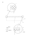
- FIG. 1 is a cross-sectional view of one embodiment of a transparent conductive layer of the present invention
- FIG. 2 is a cross-sectional view of a transparent conductive film having a transparent conductive layer shown in FIG. 1
- 4 is a graph showing the relationship between the amount of introduced oxygen and the specific resistance in reactive sputtering of Example 1.
- a transparent conductive layer 1 that is one embodiment of the present invention will be described with reference to FIG.
- This transparent conductive layer 1 extends in the plane direction.
- the plane direction is perpendicular to the thickness direction.
- the transparent conductive layer 1 is crystalline.
- the transparent conductive layer 1 contains an inorganic oxide.
- inorganic oxides include metal oxides.
- the metal oxide contains at least one metal selected from the group consisting of In, Sn, Zn, Ga, Sb, Nb, Ti, Si, Zr, Mg, Al, Au, Ag, Cu, Pd and W .
- the material of the transparent conductive layer 1 is preferably indium zinc composite oxide (IZO), indium gallium zinc composite oxide (IGZO), indium gallium composite oxide (IGO), indium tin composite oxide. (ITO) and antimony tin composite oxide (ATO), preferably indium tin composite oxide (ITO) from the viewpoint of improving etching properties.
- the content of tin oxide (SnO 2 ) in the indium-tin composite oxide is, for example, 0.5% by mass or more, preferably 3% by mass or more, and more preferably It is 6% by mass or more, more preferably 8% by mass or more, and is, for example, less than 50% by mass, preferably 25% by mass or less, more preferably 15% by mass or less. If the content of tin oxide in the indium-tin composite oxide is at least the above-described lower limit, the etchability is excellent. When the content of tin oxide (SnO 2 ) in the indium-tin composite oxide is equal to or less than the upper limit described above, it is easy to achieve both excellent resistance characteristics and etching properties of the transparent conductive layer 1 .
- the above inorganic oxide contains a rare gas having an atomic number higher than that of argon.
- a rare gas 2 having an atomic number greater than that of argon exists throughout the transparent conductive layer 1 in the thickness direction, as shown in the upper enlarged view of FIG.
- the transparent conductive layer 1 is a composition in which an inorganic oxide (preferably a metal oxide) is mixed with a noble gas having an atomic number greater than that of argon.
- an inorganic oxide preferably a metal oxide
- Rare gases with atomic numbers greater than argon include, for example, krypton, xenon, and radon. These can be used alone or in combination.
- the noble gas having an atomic number greater than that of argon is preferably krypton and xenon, and more preferably krypton (Kr) from the viewpoint of obtaining low cost and excellent electrical conductivity.
- the method of identifying noble gases with atomic numbers greater than argon is not limited.
- Rutherford Backscattering Spectrometry, Secondary Ion Mass Spectrometry, Laser Resonance Ionization Mass Spectrometry, and/or X-ray fluorescence spectrometry show that noble gases with higher atomic numbers than argon in the transparent conductive layer 1 Identified (existence or non-existence is determined), preferably by fluorescent X-ray analysis from the viewpoint of analysis simplicity. Details of the fluorescent X-ray analysis are described in Examples.
- the content ratio of the rare gas having an atomic number larger than that of argon in the inorganic oxide (transparent conductive layer 1) is, for example, 0.0001 atom % or more, preferably 0.001 atom % or more, or, for example, 1. 0 atom% or less, more preferably 0.7 atom% or less, still more preferably 0.5 atom% or less, even more preferably 0.3 atom% or less, particularly preferably 0.2 atom% or less, most preferably 0 .15 atom % or less. If the content ratio of the noble gas having an atomic number larger than that of argon in the inorganic oxide (transparent conductive layer 1) is within the above range, the etchability of the transparent conductive layer 1 can be improved.
- the rare gas 2 having an atomic number greater than that of argon is present (distributed) in a part of the transparent conductive layer 1 in the thickness direction, as shown in the lower enlarged view of FIG.
- the transparent conductive layer 1 has a first region 3 and a second region 4 in order toward one side in the thickness direction.
- the first region 3 contains a rare gas 2 with an atomic number greater than that of argon. Note that the first region 3 is allowed to contain argon. Preferably, the first region 3 does not contain argon.
- the thickness ratio of the first region 3 in the transparent conductive layer 1 is, for example, 0.95 or less, preferably 0.8 or less, more preferably 0.7 or less, still more preferably 0.6 or less, and particularly It is preferably 0.48 or less, and is, for example, 0.01 or more, preferably 0.1 or more, more preferably 0.3 or more.
- the thickness of the first region 3 is, for example, 5 nm or more, preferably 10 nm or more, more preferably 20 nm or more, still more preferably 30 nm or more, even more preferably over 40 nm, particularly preferably 50 nm or more, Also, for example, it is less than 300 nm, preferably 250 nm or less, more preferably 150 nm or less, even more preferably 100 nm or less, and even more preferably 70 nm or less.
- the content of the rare gas having an atomic number higher than that of argon in the first region 3 is, for example, 0.0001 atom% or more, preferably 0.001 atom% or more, and, for example, 1.0 atom% or less, or more. preferably 0.7 atom% or less, more preferably 0.5 atom% or less, even more preferably 0.3 atom% or less, particularly preferably 0.2 atom% or less, most preferably 0.15 atom% or less be. If the content ratio of the rare gas having an atomic number larger than that of argon in the first region 3 is within the above range, the etchability of the first region 3 can be improved.
- the second region 4 does not contain a rare gas 2 with an atomic number greater than that of argon.
- the second region 4, contains, for example, argon or no argon.
- the second region 4 does not contain a noble gas 2 with an atomic number greater than argon, it contains argon.
- the presence of argon is confirmed, for example, by performing Rutherford backscattering analysis.
- the ratio of the second region 4 to the thickness of the first region 3 is, for example, 0.99 or more, preferably 0.9 or more, preferably 1.2 or more, and for example, 2.0 or less, preferably is 1.5 or less.
- the thickness of the second region 4 is, for example, 5 nm or more, preferably 10 nm or more, more preferably 20 nm or more, still more preferably 30 nm or more, even more preferably over 40 nm, particularly preferably 50 nm or more, Also, for example, it is less than 300 nm, preferably 250 nm or less, more preferably 200 nm or less, still more preferably 150 nm or less, even more preferably 100 nm or less, particularly preferably 75 nm or less, most preferably 70 nm or less. .
- the transparent conductive layer 1 (or the first region 3) contains a rare gas with an atomic number greater than that of argon. do.
- the type of rare gas contained in the transparent conductive layer 1 differs depending on the region.
- the gas contained in the transparent conductive layer 1 acts as an impurity element, and affects the crystal orientation of the transparent conductive layer 1 depending on the type and atomic size of the impurity element.
- the transparent conductive layer 1 (or the first region 3) contains a noble gas having an atomic number larger than that of argon, so that the orientation in the (440) plane can be controlled appropriately, and as a result, (the first region 3 ) improves the etchability of the transparent conductive layer 1 .
- the transparent conductive layer 1 when the transparent conductive layer 1 is subjected to X-ray diffraction, the half width of the peak in the (440) plane is 0.27 degrees or less, so the transparent conductive layer 1 has excellent etching properties.
- the half width of the peak in the (440) plane is preferably 0.26 degrees or less, more preferably 0.25 degrees or less, and still more preferably 0.24 degrees. Below, it is particularly preferably 0.23 degrees or less, most preferably 0.22 degrees or less.
- the half width of the peak in the (440) plane is, for example, 0.01 degrees or more, preferably 0.05 degrees or more, more preferably 0.10 degrees. 0.15 degrees or more, more preferably 0.15 degrees or more.
- side etching of the transparent conductive layer 1 due to excessive solubility can be suppressed.
- Side etching is one of the phenomena in which the transparent conductive layer 1 is excessively removed when the transparent conductive layer 1 is processed into a pattern shape by etching. Specifically, an etching resist having a pattern is formed on one surface of the transparent conductive layer 1 in the thickness direction, and the transparent conductive layer 1 exposed from the pattern is brought into contact with the etching liquid, and the etching liquid is exposed to the transparent conductive layer 1 described above. is removed toward the other side, the transparent conductive layer 1 in contact with the edge of the etching resist is also removed excessively.
- the method for setting the half width of the peak in the (440) plane in X-ray diffraction to the above range is not limited.
- the half-value width of the peak in the (440) plane of X-ray diffraction is measured based on the description of the later examples.
- Dissolution time of transparent conductive layer 1 The dissolution time when the transparent conductive layer 1 is immersed in 7 mass% hydrochloric acid is, for example, 20 (seconds/nm) or less, preferably 18 (seconds/nm) or less. More preferably, it is 17 (seconds/nm) or less, still more preferably 16 (seconds/nm) or less, and is, for example, 1 (seconds/nm) or more.
- Short dissolution time means excellent etchability. Measurement of dissolution time is described in a later example.
- the crystal grain size of the transparent conductive layer 1 is, for example, 0.05 ⁇ m or more, preferably 0.1 ⁇ m or more, and more preferably 0.15 ⁇ m or more. , 3 ⁇ m or less, preferably 1 ⁇ m or less, more preferably 0.5 ⁇ m or less, even more preferably less than 0.4 ⁇ m, even more preferably 0.3 ⁇ m or less, particularly preferably 0.25 ⁇ m or less. If the crystal grain size is at least the above-described lower limit, the etchability is excellent. If the crystal grain size is equal to or less than the upper limit described above, the transparent conductive layer 1 is less likely to crack even if the substrate 6 containing a flexible resin is employed.
- the crystal grain size is obtained by, for example, FE-SEM observation. The details of the method of determination will be described in Examples below.
- the thickness of the transparent conductive layer 1 is, for example, 15 nm or more, preferably 35 nm or more, more preferably 50 nm or more, even more preferably 75 nm or more, even more preferably 100 nm or more, particularly preferably 120 nm or more.
- the thickness of the transparent conductive layer 1 is, for example, 500 nm or less, preferably 300 nm or less, more preferably 250 nm or less, more preferably 200 nm or less, even more preferably 150 nm or less, even more preferably 140 nm or less, and particularly preferably 140 nm or less. is 135 nm or less.
- the total light transmittance of the transparent conductive layer 1 is, for example, 75% or higher, preferably 80% or higher, more preferably 85% or higher, still more preferably 90% or higher.
- the upper limit of the total light transmittance of the transparent conductive layer 1 is not limited.
- the upper limit of the total light transmittance of the transparent conductive layer 1 is, for example, 100%.
- the specific resistance of the transparent conductive layer 1 is, for example, 5.0 ⁇ 10 ⁇ 4 ⁇ cm or less, preferably 3 ⁇ 10 ⁇ 4 ⁇ cm or less, or 0.1 ⁇ 10 ⁇ 4 ⁇ cm or less. ⁇ cm or more, preferably 1.1 ⁇ 10 ⁇ 4 ⁇ cm or more. A specific resistance is measured by the four-probe method.
- the transparent conductive film 5 extends in the plane direction.
- the transparent conductive film 5 includes a substrate 6 and a transparent conductive layer 1 in order toward one side in the thickness direction. That is, in this embodiment, in the transparent conductive film 5, the substrate 6 and the transparent conductive layer 1 are arranged in order toward one side in the thickness direction. In this embodiment, the transparent conductive film 5 includes only the substrate 6 and the transparent conductive layer 1 .
- the substrate 6 forms the other surface of the transparent conductive film 5 in the thickness direction.
- the base material 6 improves the mechanical strength of the transparent conductive film 5 .
- the base material 6 extends in the surface direction.
- the base material 6 contains resin, for example. If the substrate 6 contains a resin, both excellent resistance characteristics and etchability in the transparent conductive layer 1 can be achieved.
- the base material 6 consists of resin. If the base material 6 is made of a resin, the transparent conductive film 5 having flexibility can be realized in addition to achieving both excellent resistance characteristics and etchability in the transparent conductive layer 1 .
- the resin will be explained later.
- substrate 6 is not adjacent to a glass plate (not shown). In this embodiment, the other surface of the substrate 6 in the thickness direction does not come into contact with the glass plate.
- the base material 6 includes a base sheet 61 and a functional layer 60 in order in the thickness direction.
- the functional layer 60 is a single layer.
- the functional layer 60 contacts one side of the base sheet 61 in the thickness direction.
- Functional layer 60 is preferably hard coat layer 62 .
- the base material 6 preferably includes a base material sheet 61 and a hard coat layer 62 in order toward the other side in the thickness direction.
- the base sheet 61 has flexibility.
- Examples of the base sheet 61 include a resin film.
- the resin in the resin film is not limited.
- Examples of resins include polyester resins, acrylic resins, olefin resins, polycarbonate resins, polyethersulfone resins, polyarylate resins, melamine resins, polyamide resins, polyimide resins, cellulose resins, polystyrene resins, and norbornene resins. From the viewpoint of transparency and mechanical strength, the resin is preferably a polyester resin.
- Polyester resins include, for example, polyethylene terephthalate (PET), polybutylene terephthalate, and polyethylene naphthalate, preferably PET.
- the thickness of the base sheet 61 is preferably 1 ⁇ m or more, more preferably 10 ⁇ m or more, and even more preferably 30 ⁇ m or more.
- the thickness of the base sheet 61 is preferably 300 ⁇ m or less, more preferably 200 ⁇ m or less, still more preferably 150 ⁇ m or less, and particularly preferably 100 ⁇ m or less.
- the ratio of the thickness of the base sheet 61 to the thickness of the base material 6 is, for example, 0% or more, preferably 50% or more, more preferably 80% or more, and for example, 99.99% or less, preferably. is 99% or less.
- the hard coat layer 62 makes it difficult for scratches to form on one side of the transparent conductive layer 1 in the thickness direction.
- the hard coat layer 62 contacts one side of the base sheet 61 in the thickness direction.
- the hard coat layer 62 is made of resin.
- the hard coat layer 62 is, for example, a cured product layer of a curable composition containing a curable resin.
- curable resins include acrylic resins, urethane resins, amide resins, silicone resins, epoxy resins, and melamine resins.
- the curable resin preferably includes an acrylic resin.
- the thickness of the hard coat layer 62 is, for example, 0.1 ⁇ m or more, preferably 0.5 ⁇ m or more, and is, for example, 10 ⁇ m or less, preferably 3 ⁇ m or less.
- the ratio of the thickness of the hard coat layer 62 to the thickness of the base sheet 61 is, for example, 0.1% or more, preferably 1% or more, and is, for example, 100% or less, preferably 50% or less. .
- the thickness of the hard coat layer 62 corresponds to the thickness of the functional layer 60 .
- Thickness of Base Material 6 More preferably, it is 100 ⁇ m or less.
- the thickness of the base material 6 is the total thickness of the base material sheet 61 and the hard coat layer 62 .
- the total light transmittance of the substrate 6 is, for example, 75% or higher, preferably 80% or higher, more preferably 85% or higher, and still more preferably 90% or higher. .
- the upper limit of the total light transmittance of the base material 6 is not limited.
- the upper limit of the total light transmittance of the substrate 6 is, for example, 100%.
- the total light transmittance of the substrate 6 is obtained based on JIS K 7375-2008.
- the total light transmittance of the following members is obtained based on the same method as above.
- a commercially available product can be used for the base material 6 .
- the transparent conductive layer 1 forms one surface of the transparent conductive film 5 in the thickness direction.
- the transparent conductive layer 1 is arranged on one side of the base material 6 in the thickness direction.
- the transparent conductive layer 1 contacts one surface of the base material 6 in the thickness direction. That is, the other surface of the transparent conductive layer 1 in the thickness direction contacts the substrate 6 .
- the other surface of the transparent conductive layer 1 is in contact with one surface of the hard coat layer 62 (functional layer 60) in the thickness direction.
- the first region 3 is the base material 6 in the thickness direction. placed on one side.
- the first region 3 contacts one surface of the hard coat layer 62 (see FIG. 2) in the thickness direction.
- the transparent conductive film 5 is formed from the base material A sheet 61, a hard coat layer 62, a first region 3, and a second region 4 are provided in order toward one side in the thickness direction. That is, the second region 4 is arranged on the opposite side of the base material 6 with respect to the first region 3 in the thickness direction.
- Thickness of transparent conductive film 5 and other physical properties It is preferably 200 ⁇ m or less, more preferably 100 ⁇ m or less.
- the total light transmittance of the transparent conductive film 5 is, for example, 75% or more, preferably 80% or more, and is, for example, 100% or less.
- each layer is arranged by a roll-to-roll method.
- the base material 6 is prepared. Specifically, a curable composition is applied to one surface of the base sheet 61 . After that, the curable resin in the curable composition is cured by heat or ultraviolet irradiation. As a result, the hard coat layer 62 is formed on one side of the base sheet 61 . The base material 6 is prepared by this.
- the transparent conductive layer 1 is formed on one surface of the substrate 6 in the thickness direction. Specifically, first, an amorphous transparent conductive layer is formed on one side of the substrate 6 in the thickness direction, and then the amorphous transparent conductive layer is converted into a crystalline material to form the transparent conductive layer 1. .
- amorphous transparent conductive layer Formation of amorphous transparent conductive layer (sputtering process) To form the amorphous transparent conductive layer, for example, sputtering, preferably reactive sputtering, is carried out.
- a sputtering apparatus is used for sputtering.
- the sputtering apparatus includes a single film-forming roll and a single film-forming chamber.
- the deposition chamber can supply sputtering gas into the deposition chamber.
- Sputtering gases include noble gases having atomic numbers higher than argon.
- Noble gases having atomic numbers greater than argon include, for example, krypton, xenon, and radon, preferably krypton (Kr).
- the sputtering gas preferably does not contain argon.
- the sputtering gas is preferably mixed with a reactive gas.
- Reactive gases include, for example, oxygen.
- the ratio of the introduction amount of the reactive gas to the total introduction amount of the sputtering gas and the reactive gas is, for example, 0.1 flow % or more, preferably 0.5 flow % or more, and for example, 5.0 flow rate. %, preferably 4.0 flow % or less, more preferably 3.5 flow % or less.
- a single target is placed in a single deposition chamber.
- the target is, for example, (a sintered body of) the metal oxide described above.
- a first sputtering process and a second sputtering process are performed in order.
- a sputtering apparatus is provided with first and second deposition chambers.
- the first and second film forming chambers are arranged in order toward the downstream side in the conveying direction of the substrate 6 .
- a first sputtering gas is introduced into the first deposition chamber.
- the first sputtering gas includes a noble gas having an atomic number greater than argon.
- the first sputtering gas is a noble gas with an atomic number greater than argon.
- a first region 3 is formed by the first sputtering step.
- a second sputtering gas is introduced into the second deposition chamber.
- the second sputtering gas contains argon.
- the second sputtering gas is argon.
- a second region 4 is formed on one side of the first region 3 by the second sputtering process.
- the atmospheric pressure in the sputtering apparatus is, for example, 1.0 Pa or less and, for example, 0.01 Pa or more.
- the amorphous transparent conductive layer includes first region 3 and second region 4 .
- the amorphous transparent conductive layer (laminate comprising) is heated.
- the heating temperature is, for example, 80° C. or higher, preferably 110° C. or higher, more preferably 130° C. or higher, particularly preferably 150° C. or higher, and for example, 200° C. or lower, preferably It is 180° C. or lower, more preferably 175° C. or lower, still more preferably 170° C. or lower.
- the heating time is, for example, 1 minute or longer, preferably 3 minutes or longer, more preferably 5 minutes or longer, and is, for example, 5 hours or shorter, preferably 3 hours or shorter, more preferably 2 hours or shorter. be. Heating is performed, for example, under vacuum or in the atmosphere. From the viewpoint of obtaining excellent etching properties of the transparent conductive layer 1, the heating is preferably carried out in the atmosphere.
- the transparent conductive film 5 having an amorphous transparent conductive layer is left in the atmosphere at a temperature of 20° C. or more and less than 80° C. for, for example, 10 hours or more, preferably 24 hours or more.
- a crystalline transparent conductive layer can also be converted to a crystalline one.
- the transparent conductive film 5 is used for articles, for example.
- Articles include optical articles. More specifically, examples of articles include touch sensors, electromagnetic wave shields, light control elements, photoelectric conversion elements, heat ray control members, light-transmitting antenna members, light-transmitting heater members, image display devices, and lighting.
- the transparent conductive layer 1 provided on the transparent conductive film 5 has excellent etching properties. In other words, the dissolution time of the transparent conductive layer 1 is short.
- the transparent conductive layer 1 is etched and patterned according to the type of article described above.
- the transparent conductive film 5 includes the substrate 6, the second region 4, and the first region 3 in order toward one side in the thickness direction.
- the transparent conductive layer 1 has a repeating structure of the first regions 3 and the second regions 4 .
- the functional layer 60 is multi-layered.
- the functional layer 60 is arranged on one side and the other side of the base sheet 61 in the thickness direction.
- the functional layer 60 includes an optical adjustment layer and a hard coat layer.
- the optical adjustment layer is arranged on one side of the base sheet 61 .
- the hard coat layer is arranged on the other side of the base sheet 61 .
- Example 1 A substrate 6 having a thickness of 52 ⁇ m was prepared.
- a base sheet 61 (thickness: 50 ⁇ m, manufactured by Toray Industries, Inc.) made of PET was prepared.
- a hard coat composition (ultraviolet curable resin containing an acrylic resin) was applied to one surface of the base sheet 61 in the thickness direction to form a coating film.
- the coating was then cured by UV irradiation.
- a hard coat layer 62 having a thickness of 2 ⁇ m was formed on one side of the base sheet 61 .
- the base material 6 having the base material sheet 61 and the hard coat layer 62 in order toward one side in the thickness direction was produced.
- An amorphous transparent conductive layer was formed on one side of the substrate 6 by reactive sputtering (implementation of the sputtering process).
- the conditions for reactive sputtering are as follows.
- a sintered body of indium oxide and tin oxide was used as a target.
- the tin oxide concentration in the sintered body was 10% by mass.
- a DC power supply was used to apply voltage to the target.
- the horizontal magnetic field strength on the target was set to 90 mT.
- the inside of the film forming chamber in the DC magnetron sputtering apparatus was evacuated until the final degree of vacuum in the film forming chamber reached 0.9 ⁇ 10 ⁇ 4 Pa, and the substrate 6 was degassed. After that, Kr as a sputtering gas and oxygen as a reactive gas were introduced into the film forming chamber, and the atmospheric pressure in the film forming chamber was set to 0.2 Pa.
- the ratio of the introduced amount of oxygen to the total introduced amount of Kr and oxygen introduced into the film forming chamber was about 2.5 flow rate %.
- the oxygen introduction amount is within the region X of the resistivity-oxygen introduction amount curve, and the resistivity of the amorphous krypton-containing transparent conductive layer is 6.6 ⁇ 10 ⁇ 4 ⁇ cm. adjusted to be The specific resistance-oxygen introduction amount curve shown in FIG.
- the dependence of the specific resistance of the krypton-containing transparent conductive layer on the amount of introduced oxygen can be investigated in advance.
- the laminate was heated in a hot air oven at 160°C.
- the amorphous transparent conductive layer was converted to a crystalline transparent conductive layer 1 .
- the thickness of the transparent conductive layer 1 was 130 nm.
- a transparent conductive film 5 which includes the substrate 6 and the amorphous transparent conductive layer in order toward one side in the thickness direction.
- Example 2 A transparent conductive film was produced in the same manner as in Example 1. However, in the formation of the amorphous transparent conductive layer, the first sputtering step and the second sputtering step were sequentially performed with the following changes.
- a first sputtering step was performed in the same manner as in Example 1. However, the oxygen introduction amount is changed so that the specific resistance of the amorphous krypton-containing transparent conductive layer is 6.5 ⁇ 10 -4 ⁇ cm, and the ratio of the oxygen introduction amount to the total introduction amount of Kr and oxygen was changed to 2.6% flow rate.
- An amorphous first region 3 was formed by a first sputtering step. The thickness of the first region 3 was 55 nm.
- a second sputtering process was performed.
- the sputtering gas was changed to argon
- the atmospheric pressure in the sputtering film forming apparatus was changed to 0.4 Pa
- the oxygen introduction amount was changed so that the resistivity of the amorphous second region 4 was 6.5 ⁇ 10 ⁇ 4 ⁇ cm, and the ratio of the introduced amount of oxygen to the total introduced amount of Ar and oxygen was changed to 1.5 flow rate %.
- a second sputtering step formed an amorphous second region 4 .
- the thickness of the second region 4 was 75 nm.
- the sputtering gas was changed to argon, and the pressure inside the sputtering film forming apparatus was changed to 0.4 Pa.
- the thickness of the first region 3 was 19 nm.
- the tin oxide concentration in the target was changed to 3% by mass.
- the thickness of the second region 4 was 3 nm.
- the tin oxide concentration in the sintered body was changed to 3% by mass.
- the oxygen introduction amount was changed so that the resistivity in the first region 3 was 6.6 ⁇ 10 ⁇ 4 ⁇ cm, and the ratio of the oxygen introduction amount to the total introduction amount of Kr and oxygen was set to 2.5 flow rate %. changed.
- the amorphous transparent conductive layer was crystallized by bringing it into contact with a heating roll in a vacuum heating device. The heating temperature was 160° C. and the heating time was 0.1 hour. The thickness of the first region 3 was 11 nm.
- the sputtering gas was changed from Kr to argon.
- the thickness of the second region 4 was 11 nm.
- the thickness of the transparent conductive layer 1 was measured by FE-TEM observation. Specifically, first, a cross-sectional observation sample of the transparent conductive layer 1 was produced by the FIB microsampling method. In the FIB microsampling method, an FIB device (trade name “FB2200”, manufactured by Hitachi) was used, and the acceleration voltage was set to 10 kV. Next, the thickness of the transparent conductive layer 1 in the sample for cross-sectional observation was measured by FE-TEM observation. In the FE-TEM observation, an FE-TEM apparatus (trade name “JEM-2800” manufactured by JEOL) was used with an acceleration voltage of 200 kV.
- Example 2 Comparative Example 1, and Comparative Example 2, before forming the second region 4, a sample for cross-sectional observation was prepared from the first region 3, and the sample was observed by FE-TEM. The thickness of 1 region 3 was calculated.
- the thickness of the second region 4 was calculated.
- the X-ray peak profile was obtained by subtracting the background derived from the base material 6 (the base material 6 heated under the same conditions as the transparent conductive layer 1 of each example and each comparative example). After that, using analysis software (software name "SmartLab Studio II”), create an X-ray diffraction peak profile corresponding to the (440) plane so that 2 ⁇ is in the range of 49.8 ° to 51.8 °, By fitting the X-ray diffraction peak (peak shape: split Pearson VII function, background type: B-spline, fitting conditions: automatic), the half width of the X-ray diffraction peak in the (440) plane (FWHM, unit ;°) was obtained.
- analysis software software name "SmartLab Studio II”
- ⁇ Crystal grain size> One surface of the transparent conductive layer 1 was observed with an FE-SEM (manufactured by Hitachi, SU8020) to determine the crystal grain size of the transparent conductive layer 1 . Specifically, after fixing the transparent conductive layer 1 to a table, surface FE-SEM observation (acceleration voltage: 0.8 kV, observed image: secondary electron image) is performed, and the transparent conductive layer 1 is observed in plan view. I took a picture. The magnification was adjusted so that the grains could be clearly identified.
- the area of the region is obtained from the number of pixels present in the region defined by the grain boundary (region within each grain boundary), and the area of the same area as the area is obtained.
- the diameter of the circle was determined as the crystal grain size (equivalent circle diameter). The results are listed in Table 1.
- etchability ⁇ Dissolution time (etchability)> The etchability of the transparent conductive layer 1 was evaluated by measuring the dissolution time (sec/nm) of the transparent conductive layer 1 . The results are listed in Table 1.
- a cycle comprising the following first step, second step, and third step in this order was performed once or multiple times.
- the third step if it was determined that the etching was completed, the corresponding cycle was terminated. On the other hand, if the third step determined that the etching was not complete, the cycle was repeated.
- First step The transparent conductive film 5 was immersed in hydrochloric acid having a concentration of 7% by mass. The immersion temperature was 35°C. The immersion time was 30 seconds. Second step: The transparent conductive film 5 was washed with water and then dried. Third step: On one surface (exposed surface) of the transparent conductive layer 1 of the transparent conductive film 5, a surface resistance measurement tester is used to measure the resistance (inter-terminal resistance) between a pair of terminals separated by a distance of 15 mm. bottom.
- the third step when the measured inter-terminal resistance exceeds 100 k ⁇ , or when the measurement is impossible, in the first step of the cycle to which the third step belongs, dissolution (etching) of the transparent conductive layer 1 determined to be complete.
- the dissolution time (more specifically, the dissolution time per unit thickness) was obtained by dividing the cumulative immersion time (dissolution time) of a plurality of first steps by the thickness of the transparent conductive layer 1 .
- the shorter the dissolution time the better the etchability of the transparent conductive layer 1 .
- Transparent conductive films are used in optical articles.
Landscapes
- Chemical & Material Sciences (AREA)
- Engineering & Computer Science (AREA)
- Manufacturing & Machinery (AREA)
- Spectroscopy & Molecular Physics (AREA)
- Dispersion Chemistry (AREA)
- Physics & Mathematics (AREA)
- Organic Chemistry (AREA)
- Polymers & Plastics (AREA)
- Medicinal Chemistry (AREA)
- Chemical Kinetics & Catalysis (AREA)
- Health & Medical Sciences (AREA)
- Materials Engineering (AREA)
- Non-Insulated Conductors (AREA)
- Laminated Bodies (AREA)
- Physical Vapour Deposition (AREA)
- Conductive Materials (AREA)
Priority Applications (5)
| Application Number | Priority Date | Filing Date | Title |
|---|---|---|---|
| JP2023548479A JP7492089B2 (ja) | 2021-09-17 | 2022-09-14 | 透明導電層および透明導電性フィルム |
| KR1020237032668A KR20240058046A (ko) | 2021-09-17 | 2022-09-14 | 투명 도전층 및 투명 도전성 필름 |
| CN202280024211.1A CN117063246A (zh) | 2021-09-17 | 2022-09-14 | 透明导电层及透明导电性薄膜 |
| JP2024079989A JP2024103523A (ja) | 2021-09-17 | 2024-05-16 | 透明導電層、透明導電性フィルム、物品および光電変換素子 |
| JP2025198959A JP2026026105A (ja) | 2021-09-17 | 2025-11-19 | 透明導電層および透明導電性フィルム |
Applications Claiming Priority (2)
| Application Number | Priority Date | Filing Date | Title |
|---|---|---|---|
| JP2021152346 | 2021-09-17 | ||
| JP2021-152346 | 2021-09-17 |
Publications (1)
| Publication Number | Publication Date |
|---|---|
| WO2023042845A1 true WO2023042845A1 (ja) | 2023-03-23 |
Family
ID=85602909
Family Applications (1)
| Application Number | Title | Priority Date | Filing Date |
|---|---|---|---|
| PCT/JP2022/034348 Ceased WO2023042845A1 (ja) | 2021-09-17 | 2022-09-14 | 透明導電層および透明導電性フィルム |
Country Status (4)
| Country | Link |
|---|---|
| JP (3) | JP7492089B2 (https=) |
| KR (1) | KR20240058046A (https=) |
| CN (1) | CN117063246A (https=) |
| WO (1) | WO2023042845A1 (https=) |
Families Citing this family (1)
| Publication number | Priority date | Publication date | Assignee | Title |
|---|---|---|---|---|
| KR20240058046A (ko) * | 2021-09-17 | 2024-05-07 | 닛토덴코 가부시키가이샤 | 투명 도전층 및 투명 도전성 필름 |
Citations (4)
| Publication number | Priority date | Publication date | Assignee | Title |
|---|---|---|---|---|
| JPH05334924A (ja) * | 1992-05-29 | 1993-12-17 | Tonen Corp | 透明導電薄膜の製造法 |
| JP2000038654A (ja) * | 1998-07-21 | 2000-02-08 | Nippon Sheet Glass Co Ltd | 透明導電膜付き基板の製造方法、透明導電膜付き基板およびそれを用いた液晶表示素子 |
| WO2011034145A1 (ja) * | 2009-09-18 | 2011-03-24 | 三洋電機株式会社 | 太陽電池、太陽電池モジュールおよび太陽電池システム |
| JP2016136511A (ja) * | 2014-12-22 | 2016-07-28 | 日東電工株式会社 | 透明導電性フィルム |
Family Cites Families (3)
| Publication number | Priority date | Publication date | Assignee | Title |
|---|---|---|---|---|
| JP2000129427A (ja) | 1998-10-20 | 2000-05-09 | Teijin Ltd | 透明導電積層体の製造方法 |
| JP6261987B2 (ja) | 2013-01-16 | 2018-01-17 | 日東電工株式会社 | 透明導電フィルムおよびその製造方法 |
| KR20240058046A (ko) * | 2021-09-17 | 2024-05-07 | 닛토덴코 가부시키가이샤 | 투명 도전층 및 투명 도전성 필름 |
-
2022
- 2022-09-14 KR KR1020237032668A patent/KR20240058046A/ko active Pending
- 2022-09-14 WO PCT/JP2022/034348 patent/WO2023042845A1/ja not_active Ceased
- 2022-09-14 CN CN202280024211.1A patent/CN117063246A/zh active Pending
- 2022-09-14 JP JP2023548479A patent/JP7492089B2/ja active Active
-
2024
- 2024-05-16 JP JP2024079989A patent/JP2024103523A/ja active Pending
-
2025
- 2025-11-19 JP JP2025198959A patent/JP2026026105A/ja active Pending
Patent Citations (4)
| Publication number | Priority date | Publication date | Assignee | Title |
|---|---|---|---|---|
| JPH05334924A (ja) * | 1992-05-29 | 1993-12-17 | Tonen Corp | 透明導電薄膜の製造法 |
| JP2000038654A (ja) * | 1998-07-21 | 2000-02-08 | Nippon Sheet Glass Co Ltd | 透明導電膜付き基板の製造方法、透明導電膜付き基板およびそれを用いた液晶表示素子 |
| WO2011034145A1 (ja) * | 2009-09-18 | 2011-03-24 | 三洋電機株式会社 | 太陽電池、太陽電池モジュールおよび太陽電池システム |
| JP2016136511A (ja) * | 2014-12-22 | 2016-07-28 | 日東電工株式会社 | 透明導電性フィルム |
Also Published As
| Publication number | Publication date |
|---|---|
| KR20240058046A (ko) | 2024-05-07 |
| CN117063246A (zh) | 2023-11-14 |
| JP2024103523A (ja) | 2024-08-01 |
| JP2026026105A (ja) | 2026-02-16 |
| JP7492089B2 (ja) | 2024-05-28 |
| JPWO2023042845A1 (https=) | 2023-03-23 |
Similar Documents
| Publication | Publication Date | Title |
|---|---|---|
| JP7073589B2 (ja) | 透明導電層および透明導電性フィルム | |
| JP2026026105A (ja) | 透明導電層および透明導電性フィルム | |
| JP7213962B2 (ja) | 光透過性導電層および光透過性導電フィルム | |
| JP2025111820A (ja) | 透明導電性フィルムおよび透明導電性フィルムの製造方法 | |
| KR20220155279A (ko) | 투명 도전성 필름의 제조 방법 | |
| KR102665515B1 (ko) | 적층체 | |
| JP7389940B2 (ja) | 透明導電層、透明導電性フィルムおよび物品 | |
| JP7488425B2 (ja) | 透明導電性フィルムおよび物品 | |
| CN115298757A (zh) | 透光性导电膜和透明导电性薄膜 | |
| JP7419609B2 (ja) | 透明導電性フィルム | |
| JP2024131594A (ja) | 透明導電性フィルム | |
| JP2024131595A (ja) | 透明導電性フィルム | |
| CN118782297A (zh) | 透明导电性薄膜 | |
| WO2023042844A1 (ja) | 透明導電性フィルム | |
| WO2026005019A1 (ja) | 透明導電フィルムおよびその製造方法 | |
| WO2026005018A1 (ja) | 透明導電フィルムおよびその製造方法 |
Legal Events
| Date | Code | Title | Description |
|---|---|---|---|
| 121 | Ep: the epo has been informed by wipo that ep was designated in this application |
Ref document number: 22869992 Country of ref document: EP Kind code of ref document: A1 |
|
| WWE | Wipo information: entry into national phase |
Ref document number: 2023548479 Country of ref document: JP |
|
| WWE | Wipo information: entry into national phase |
Ref document number: 202280024211.1 Country of ref document: CN |
|
| NENP | Non-entry into the national phase |
Ref country code: DE |
|
| 122 | Ep: pct application non-entry in european phase |
Ref document number: 22869992 Country of ref document: EP Kind code of ref document: A1 |