WO2023042027A1 - 表示装置 - Google Patents
表示装置 Download PDFInfo
- Publication number
- WO2023042027A1 WO2023042027A1 PCT/IB2022/058311 IB2022058311W WO2023042027A1 WO 2023042027 A1 WO2023042027 A1 WO 2023042027A1 IB 2022058311 W IB2022058311 W IB 2022058311W WO 2023042027 A1 WO2023042027 A1 WO 2023042027A1
- Authority
- WO
- WIPO (PCT)
- Prior art keywords
- layer
- light
- emitting
- wiring
- emitting device
- Prior art date
Links
- 239000000463 material Substances 0.000 claims description 252
- 150000002894 organic compounds Chemical class 0.000 claims description 145
- 229910052760 oxygen Inorganic materials 0.000 claims description 28
- 239000001301 oxygen Substances 0.000 claims description 27
- QVGXLLKOCUKJST-UHFFFAOYSA-N atomic oxygen Chemical compound [O] QVGXLLKOCUKJST-UHFFFAOYSA-N 0.000 claims description 26
- 229910010272 inorganic material Inorganic materials 0.000 claims description 18
- WHXSMMKQMYFTQS-UHFFFAOYSA-N Lithium Chemical compound [Li] WHXSMMKQMYFTQS-UHFFFAOYSA-N 0.000 claims description 8
- 150000002484 inorganic compounds Chemical class 0.000 claims description 8
- 229910052744 lithium Inorganic materials 0.000 claims description 8
- 239000010410 layer Substances 0.000 description 1479
- 239000010408 film Substances 0.000 description 291
- 239000004065 semiconductor Substances 0.000 description 113
- 238000000034 method Methods 0.000 description 106
- 230000006870 function Effects 0.000 description 86
- 239000000758 substrate Substances 0.000 description 72
- 229920005989 resin Polymers 0.000 description 67
- 239000011347 resin Substances 0.000 description 67
- 238000004519 manufacturing process Methods 0.000 description 66
- 238000005530 etching Methods 0.000 description 56
- 238000002347 injection Methods 0.000 description 47
- 239000007924 injection Substances 0.000 description 47
- 230000015572 biosynthetic process Effects 0.000 description 45
- 229910052751 metal Inorganic materials 0.000 description 43
- 239000002184 metal Substances 0.000 description 39
- 239000011701 zinc Substances 0.000 description 36
- 239000013078 crystal Substances 0.000 description 33
- 239000000126 substance Substances 0.000 description 33
- 229910052738 indium Inorganic materials 0.000 description 29
- APFVFJFRJDLVQX-UHFFFAOYSA-N indium atom Chemical compound [In] APFVFJFRJDLVQX-UHFFFAOYSA-N 0.000 description 27
- XUIMIQQOPSSXEZ-UHFFFAOYSA-N Silicon Chemical compound [Si] XUIMIQQOPSSXEZ-UHFFFAOYSA-N 0.000 description 24
- 229910052710 silicon Inorganic materials 0.000 description 24
- 239000010703 silicon Substances 0.000 description 24
- 230000032258 transport Effects 0.000 description 23
- 238000000206 photolithography Methods 0.000 description 22
- IJGRMHOSHXDMSA-UHFFFAOYSA-N Atomic nitrogen Chemical compound N#N IJGRMHOSHXDMSA-UHFFFAOYSA-N 0.000 description 21
- 229910052782 aluminium Inorganic materials 0.000 description 21
- XAGFODPZIPBFFR-UHFFFAOYSA-N aluminium Chemical compound [Al] XAGFODPZIPBFFR-UHFFFAOYSA-N 0.000 description 21
- 230000002829 reductive effect Effects 0.000 description 21
- 230000000903 blocking effect Effects 0.000 description 20
- 239000004020 conductor Substances 0.000 description 20
- 239000007789 gas Substances 0.000 description 20
- 229910044991 metal oxide Inorganic materials 0.000 description 20
- 150000004706 metal oxides Chemical class 0.000 description 20
- 239000002346 layers by function Substances 0.000 description 19
- PXHVJJICTQNCMI-UHFFFAOYSA-N Nickel Chemical compound [Ni] PXHVJJICTQNCMI-UHFFFAOYSA-N 0.000 description 18
- 229910052733 gallium Inorganic materials 0.000 description 18
- 238000012545 processing Methods 0.000 description 18
- GYHNNYVSQQEPJS-UHFFFAOYSA-N Gallium Chemical compound [Ga] GYHNNYVSQQEPJS-UHFFFAOYSA-N 0.000 description 16
- XEEYBQQBJWHFJM-UHFFFAOYSA-N Iron Chemical compound [Fe] XEEYBQQBJWHFJM-UHFFFAOYSA-N 0.000 description 16
- 125000004429 atom Chemical group 0.000 description 16
- 239000012535 impurity Substances 0.000 description 16
- 230000003287 optical effect Effects 0.000 description 16
- 239000011368 organic material Substances 0.000 description 16
- 229910052725 zinc Inorganic materials 0.000 description 16
- 238000000231 atomic layer deposition Methods 0.000 description 15
- 239000003086 colorant Substances 0.000 description 15
- 230000005525 hole transport Effects 0.000 description 15
- HCHKCACWOHOZIP-UHFFFAOYSA-N Zinc Chemical compound [Zn] HCHKCACWOHOZIP-UHFFFAOYSA-N 0.000 description 14
- 238000010586 diagram Methods 0.000 description 14
- VYPSYNLAJGMNEJ-UHFFFAOYSA-N Silicium dioxide Chemical compound O=[Si]=O VYPSYNLAJGMNEJ-UHFFFAOYSA-N 0.000 description 13
- ATJFFYVFTNAWJD-UHFFFAOYSA-N Tin Chemical compound [Sn] ATJFFYVFTNAWJD-UHFFFAOYSA-N 0.000 description 13
- 229910045601 alloy Inorganic materials 0.000 description 13
- 239000000956 alloy Substances 0.000 description 13
- -1 etc.) Substances 0.000 description 13
- 229910052718 tin Inorganic materials 0.000 description 13
- KDLHZDBZIXYQEI-UHFFFAOYSA-N Palladium Chemical compound [Pd] KDLHZDBZIXYQEI-UHFFFAOYSA-N 0.000 description 12
- 239000000853 adhesive Substances 0.000 description 12
- 230000001070 adhesive effect Effects 0.000 description 12
- 229910052783 alkali metal Inorganic materials 0.000 description 12
- 150000001340 alkali metals Chemical class 0.000 description 12
- 229910052784 alkaline earth metal Inorganic materials 0.000 description 12
- 150000001342 alkaline earth metals Chemical class 0.000 description 12
- 239000011159 matrix material Substances 0.000 description 12
- 230000008569 process Effects 0.000 description 12
- 239000011241 protective layer Substances 0.000 description 12
- 230000000694 effects Effects 0.000 description 11
- 238000004544 sputter deposition Methods 0.000 description 11
- 239000010409 thin film Substances 0.000 description 11
- 239000010936 titanium Substances 0.000 description 11
- 229910052721 tungsten Inorganic materials 0.000 description 11
- 239000010937 tungsten Substances 0.000 description 11
- 238000001039 wet etching Methods 0.000 description 11
- RYGMFSIKBFXOCR-UHFFFAOYSA-N Copper Chemical compound [Cu] RYGMFSIKBFXOCR-UHFFFAOYSA-N 0.000 description 10
- RTAQQCXQSZGOHL-UHFFFAOYSA-N Titanium Chemical compound [Ti] RTAQQCXQSZGOHL-UHFFFAOYSA-N 0.000 description 10
- 238000002441 X-ray diffraction Methods 0.000 description 10
- 150000001875 compounds Chemical class 0.000 description 10
- 239000010949 copper Substances 0.000 description 10
- 238000001312 dry etching Methods 0.000 description 10
- 238000010894 electron beam technology Methods 0.000 description 10
- 239000011147 inorganic material Substances 0.000 description 10
- 239000000203 mixture Substances 0.000 description 10
- 229910052757 nitrogen Inorganic materials 0.000 description 10
- BASFCYQUMIYNBI-UHFFFAOYSA-N platinum Chemical compound [Pt] BASFCYQUMIYNBI-UHFFFAOYSA-N 0.000 description 10
- 230000001681 protective effect Effects 0.000 description 10
- 239000002356 single layer Substances 0.000 description 10
- 229910052719 titanium Inorganic materials 0.000 description 10
- WFKWXMTUELFFGS-UHFFFAOYSA-N tungsten Chemical compound [W] WFKWXMTUELFFGS-UHFFFAOYSA-N 0.000 description 10
- 229910052727 yttrium Inorganic materials 0.000 description 10
- VWQVUPCCIRVNHF-UHFFFAOYSA-N yttrium atom Chemical compound [Y] VWQVUPCCIRVNHF-UHFFFAOYSA-N 0.000 description 10
- ZOKXTWBITQBERF-UHFFFAOYSA-N Molybdenum Chemical compound [Mo] ZOKXTWBITQBERF-UHFFFAOYSA-N 0.000 description 9
- BQCADISMDOOEFD-UHFFFAOYSA-N Silver Chemical compound [Ag] BQCADISMDOOEFD-UHFFFAOYSA-N 0.000 description 9
- XLOMVQKBTHCTTD-UHFFFAOYSA-N Zinc monoxide Chemical compound [Zn]=O XLOMVQKBTHCTTD-UHFFFAOYSA-N 0.000 description 9
- 229910052802 copper Inorganic materials 0.000 description 9
- 230000007547 defect Effects 0.000 description 9
- 150000002739 metals Chemical class 0.000 description 9
- 229910052750 molybdenum Inorganic materials 0.000 description 9
- 239000011733 molybdenum Substances 0.000 description 9
- 229910052759 nickel Inorganic materials 0.000 description 9
- 150000004767 nitrides Chemical class 0.000 description 9
- 229910052814 silicon oxide Inorganic materials 0.000 description 9
- 229910052709 silver Inorganic materials 0.000 description 9
- 239000004332 silver Substances 0.000 description 9
- 239000012790 adhesive layer Substances 0.000 description 8
- 239000003990 capacitor Substances 0.000 description 8
- 238000005229 chemical vapour deposition Methods 0.000 description 8
- 230000000295 complement effect Effects 0.000 description 8
- 238000000605 extraction Methods 0.000 description 8
- 239000001257 hydrogen Substances 0.000 description 8
- 229910052739 hydrogen Inorganic materials 0.000 description 8
- 229910052742 iron Inorganic materials 0.000 description 8
- TWNQGVIAIRXVLR-UHFFFAOYSA-N oxo(oxoalumanyloxy)alumane Chemical compound O=[Al]O[Al]=O TWNQGVIAIRXVLR-UHFFFAOYSA-N 0.000 description 8
- 229910052715 tantalum Inorganic materials 0.000 description 8
- GUVRBAGPIYLISA-UHFFFAOYSA-N tantalum atom Chemical compound [Ta] GUVRBAGPIYLISA-UHFFFAOYSA-N 0.000 description 8
- XLYOFNOQVPJJNP-UHFFFAOYSA-N water Substances O XLYOFNOQVPJJNP-UHFFFAOYSA-N 0.000 description 8
- UFHFLCQGNIYNRP-UHFFFAOYSA-N Hydrogen Chemical compound [H][H] UFHFLCQGNIYNRP-UHFFFAOYSA-N 0.000 description 7
- 229910052581 Si3N4 Inorganic materials 0.000 description 7
- 238000004380 ashing Methods 0.000 description 7
- 230000006378 damage Effects 0.000 description 7
- 229910000449 hafnium oxide Inorganic materials 0.000 description 7
- WIHZLLGSGQNAGK-UHFFFAOYSA-N hafnium(4+);oxygen(2-) Chemical compound [O-2].[O-2].[Hf+4] WIHZLLGSGQNAGK-UHFFFAOYSA-N 0.000 description 7
- 239000007769 metal material Substances 0.000 description 7
- HQVNEWCFYHHQES-UHFFFAOYSA-N silicon nitride Chemical compound N12[Si]34N5[Si]62N3[Si]51N64 HQVNEWCFYHHQES-UHFFFAOYSA-N 0.000 description 7
- 239000002904 solvent Substances 0.000 description 7
- 238000012546 transfer Methods 0.000 description 7
- 238000002834 transmittance Methods 0.000 description 7
- 238000007740 vapor deposition Methods 0.000 description 7
- MYMOFIZGZYHOMD-UHFFFAOYSA-N Dioxygen Chemical compound O=O MYMOFIZGZYHOMD-UHFFFAOYSA-N 0.000 description 6
- LFQSCWFLJHTTHZ-UHFFFAOYSA-N Ethanol Chemical compound CCO LFQSCWFLJHTTHZ-UHFFFAOYSA-N 0.000 description 6
- KFZMGEQAYNKOFK-UHFFFAOYSA-N Isopropanol Chemical compound CC(C)O KFZMGEQAYNKOFK-UHFFFAOYSA-N 0.000 description 6
- 229910052779 Neodymium Inorganic materials 0.000 description 6
- 238000000576 coating method Methods 0.000 description 6
- 229910001882 dioxygen Inorganic materials 0.000 description 6
- 235000019441 ethanol Nutrition 0.000 description 6
- 229910052735 hafnium Inorganic materials 0.000 description 6
- 238000010438 heat treatment Methods 0.000 description 6
- QEFYFXOXNSNQGX-UHFFFAOYSA-N neodymium atom Chemical compound [Nd] QEFYFXOXNSNQGX-UHFFFAOYSA-N 0.000 description 6
- 229920001721 polyimide Polymers 0.000 description 6
- XESMNQMWRSEIET-UHFFFAOYSA-N 2,9-dinaphthalen-2-yl-4,7-diphenyl-1,10-phenanthroline Chemical compound C1=CC=CC=C1C1=CC(C=2C=C3C=CC=CC3=CC=2)=NC2=C1C=CC1=C(C=3C=CC=CC=3)C=C(C=3C=C4C=CC=CC4=CC=3)N=C21 XESMNQMWRSEIET-UHFFFAOYSA-N 0.000 description 5
- DHDHJYNTEFLIHY-UHFFFAOYSA-N 4,7-diphenyl-1,10-phenanthroline Chemical compound C1=CC=CC=C1C1=CC=NC2=C1C=CC1=C(C=3C=CC=CC=3)C=CN=C21 DHDHJYNTEFLIHY-UHFFFAOYSA-N 0.000 description 5
- OKTJSMMVPCPJKN-UHFFFAOYSA-N Carbon Chemical compound [C] OKTJSMMVPCPJKN-UHFFFAOYSA-N 0.000 description 5
- VYZAMTAEIAYCRO-UHFFFAOYSA-N Chromium Chemical compound [Cr] VYZAMTAEIAYCRO-UHFFFAOYSA-N 0.000 description 5
- 229910001111 Fine metal Inorganic materials 0.000 description 5
- FYYHWMGAXLPEAU-UHFFFAOYSA-N Magnesium Chemical compound [Mg] FYYHWMGAXLPEAU-UHFFFAOYSA-N 0.000 description 5
- 229910052796 boron Inorganic materials 0.000 description 5
- 239000000969 carrier Substances 0.000 description 5
- 229910052804 chromium Inorganic materials 0.000 description 5
- 239000011651 chromium Substances 0.000 description 5
- 229910017052 cobalt Inorganic materials 0.000 description 5
- 239000010941 cobalt Substances 0.000 description 5
- GUTLYIVDDKVIGB-UHFFFAOYSA-N cobalt atom Chemical compound [Co] GUTLYIVDDKVIGB-UHFFFAOYSA-N 0.000 description 5
- 239000002131 composite material Substances 0.000 description 5
- 230000005669 field effect Effects 0.000 description 5
- 239000011521 glass Substances 0.000 description 5
- PCHJSUWPFVWCPO-UHFFFAOYSA-N gold Chemical compound [Au] PCHJSUWPFVWCPO-UHFFFAOYSA-N 0.000 description 5
- 229910052737 gold Inorganic materials 0.000 description 5
- 239000010931 gold Substances 0.000 description 5
- VBJZVLUMGGDVMO-UHFFFAOYSA-N hafnium atom Chemical compound [Hf] VBJZVLUMGGDVMO-UHFFFAOYSA-N 0.000 description 5
- 239000011777 magnesium Substances 0.000 description 5
- 229910052749 magnesium Inorganic materials 0.000 description 5
- 229910052763 palladium Inorganic materials 0.000 description 5
- 229910052697 platinum Inorganic materials 0.000 description 5
- 229920006122 polyamide resin Polymers 0.000 description 5
- 229920002050 silicone resin Polymers 0.000 description 5
- 238000001228 spectrum Methods 0.000 description 5
- 239000011787 zinc oxide Substances 0.000 description 5
- 239000004925 Acrylic resin Substances 0.000 description 4
- 229920000178 Acrylic resin Polymers 0.000 description 4
- XKRFYHLGVUSROY-UHFFFAOYSA-N Argon Chemical compound [Ar] XKRFYHLGVUSROY-UHFFFAOYSA-N 0.000 description 4
- ZOXJGFHDIHLPTG-UHFFFAOYSA-N Boron Chemical group [B] ZOXJGFHDIHLPTG-UHFFFAOYSA-N 0.000 description 4
- KRHYYFGTRYWZRS-UHFFFAOYSA-N Fluorane Chemical compound F KRHYYFGTRYWZRS-UHFFFAOYSA-N 0.000 description 4
- NBIIXXVUZAFLBC-UHFFFAOYSA-N Phosphoric acid Chemical compound OP(O)(O)=O NBIIXXVUZAFLBC-UHFFFAOYSA-N 0.000 description 4
- 239000004372 Polyvinyl alcohol Substances 0.000 description 4
- QCWXUUIWCKQGHC-UHFFFAOYSA-N Zirconium Chemical group [Zr] QCWXUUIWCKQGHC-UHFFFAOYSA-N 0.000 description 4
- 239000012298 atmosphere Substances 0.000 description 4
- XJHCXCQVJFPJIK-UHFFFAOYSA-M caesium fluoride Chemical compound [F-].[Cs+] XJHCXCQVJFPJIK-UHFFFAOYSA-M 0.000 description 4
- 229910052799 carbon Inorganic materials 0.000 description 4
- 239000011248 coating agent Substances 0.000 description 4
- 238000004891 communication Methods 0.000 description 4
- PMHQVHHXPFUNSP-UHFFFAOYSA-M copper(1+);methylsulfanylmethane;bromide Chemical compound Br[Cu].CSC PMHQVHHXPFUNSP-UHFFFAOYSA-M 0.000 description 4
- 238000011161 development Methods 0.000 description 4
- 230000018109 developmental process Effects 0.000 description 4
- 239000003822 epoxy resin Substances 0.000 description 4
- 230000009477 glass transition Effects 0.000 description 4
- 238000003384 imaging method Methods 0.000 description 4
- 150000003949 imides Chemical class 0.000 description 4
- AMGQUBHHOARCQH-UHFFFAOYSA-N indium;oxotin Chemical compound [In].[Sn]=O AMGQUBHHOARCQH-UHFFFAOYSA-N 0.000 description 4
- 229910052746 lanthanum Inorganic materials 0.000 description 4
- FZLIPJUXYLNCLC-UHFFFAOYSA-N lanthanum atom Chemical compound [La] FZLIPJUXYLNCLC-UHFFFAOYSA-N 0.000 description 4
- 239000002159 nanocrystal Substances 0.000 description 4
- 239000005011 phenolic resin Substances 0.000 description 4
- 229920002037 poly(vinyl butyral) polymer Polymers 0.000 description 4
- 229920000647 polyepoxide Polymers 0.000 description 4
- 239000009719 polyimide resin Substances 0.000 description 4
- 229920002451 polyvinyl alcohol Polymers 0.000 description 4
- 238000001004 secondary ion mass spectrometry Methods 0.000 description 4
- WGTYBPLFGIVFAS-UHFFFAOYSA-M tetramethylammonium hydroxide Chemical compound [OH-].C[N+](C)(C)C WGTYBPLFGIVFAS-UHFFFAOYSA-M 0.000 description 4
- 229910052726 zirconium Inorganic materials 0.000 description 4
- QTBSBXVTEAMEQO-UHFFFAOYSA-N Acetic acid Chemical compound CC(O)=O QTBSBXVTEAMEQO-UHFFFAOYSA-N 0.000 description 3
- 229910052684 Cerium Inorganic materials 0.000 description 3
- OKKJLVBELUTLKV-UHFFFAOYSA-N Methanol Chemical compound OC OKKJLVBELUTLKV-UHFFFAOYSA-N 0.000 description 3
- MUBZPKHOEPUJKR-UHFFFAOYSA-N Oxalic acid Chemical compound OC(=O)C(O)=O MUBZPKHOEPUJKR-UHFFFAOYSA-N 0.000 description 3
- 229910008355 Si-Sn Inorganic materials 0.000 description 3
- 229910006453 Si—Sn Inorganic materials 0.000 description 3
- 229910052769 Ytterbium Inorganic materials 0.000 description 3
- UMIVXZPTRXBADB-UHFFFAOYSA-N benzocyclobutene Chemical compound C1=CC=C2CCC2=C1 UMIVXZPTRXBADB-UHFFFAOYSA-N 0.000 description 3
- 239000000872 buffer Substances 0.000 description 3
- ZMIGMASIKSOYAM-UHFFFAOYSA-N cerium Chemical group [Ce][Ce][Ce][Ce][Ce][Ce][Ce][Ce][Ce][Ce][Ce][Ce][Ce][Ce][Ce][Ce][Ce][Ce][Ce][Ce][Ce][Ce][Ce][Ce][Ce][Ce][Ce][Ce][Ce][Ce][Ce][Ce][Ce][Ce][Ce][Ce][Ce][Ce] ZMIGMASIKSOYAM-UHFFFAOYSA-N 0.000 description 3
- 230000003111 delayed effect Effects 0.000 description 3
- AJNVQOSZGJRYEI-UHFFFAOYSA-N digallium;oxygen(2-) Chemical compound [O-2].[O-2].[O-2].[Ga+3].[Ga+3] AJNVQOSZGJRYEI-UHFFFAOYSA-N 0.000 description 3
- KPUWHANPEXNPJT-UHFFFAOYSA-N disiloxane Chemical class [SiH3]O[SiH3] KPUWHANPEXNPJT-UHFFFAOYSA-N 0.000 description 3
- 238000002003 electron diffraction Methods 0.000 description 3
- 238000002149 energy-dispersive X-ray emission spectroscopy Methods 0.000 description 3
- 230000001747 exhibiting effect Effects 0.000 description 3
- 229910001195 gallium oxide Inorganic materials 0.000 description 3
- 229910052732 germanium Inorganic materials 0.000 description 3
- GNPVGFCGXDBREM-UHFFFAOYSA-N germanium atom Chemical group [Ge] GNPVGFCGXDBREM-UHFFFAOYSA-N 0.000 description 3
- 238000001341 grazing-angle X-ray diffraction Methods 0.000 description 3
- 125000005843 halogen group Chemical group 0.000 description 3
- 239000011261 inert gas Substances 0.000 description 3
- 238000003475 lamination Methods 0.000 description 3
- 239000003446 ligand Substances 0.000 description 3
- PQXKHYXIUOZZFA-UHFFFAOYSA-M lithium fluoride Chemical compound [Li+].[F-] PQXKHYXIUOZZFA-UHFFFAOYSA-M 0.000 description 3
- 238000004768 lowest unoccupied molecular orbital Methods 0.000 description 3
- WPBNNNQJVZRUHP-UHFFFAOYSA-L manganese(2+);methyl n-[[2-(methoxycarbonylcarbamothioylamino)phenyl]carbamothioyl]carbamate;n-[2-(sulfidocarbothioylamino)ethyl]carbamodithioate Chemical compound [Mn+2].[S-]C(=S)NCCNC([S-])=S.COC(=O)NC(=S)NC1=CC=CC=C1NC(=S)NC(=O)OC WPBNNNQJVZRUHP-UHFFFAOYSA-L 0.000 description 3
- 238000005259 measurement Methods 0.000 description 3
- 229920001568 phenolic resin Polymers 0.000 description 3
- 238000000623 plasma-assisted chemical vapour deposition Methods 0.000 description 3
- 229920003023 plastic Polymers 0.000 description 3
- 239000004033 plastic Substances 0.000 description 3
- 229910021420 polycrystalline silicon Inorganic materials 0.000 description 3
- 239000002243 precursor Substances 0.000 description 3
- 238000004549 pulsed laser deposition Methods 0.000 description 3
- 239000002096 quantum dot Substances 0.000 description 3
- 239000000523 sample Substances 0.000 description 3
- 238000004528 spin coating Methods 0.000 description 3
- NAWDYIZEMPQZHO-UHFFFAOYSA-N ytterbium Chemical compound [Yb] NAWDYIZEMPQZHO-UHFFFAOYSA-N 0.000 description 3
- YVTHLONGBIQYBO-UHFFFAOYSA-N zinc indium(3+) oxygen(2-) Chemical compound [O--].[Zn++].[In+3] YVTHLONGBIQYBO-UHFFFAOYSA-N 0.000 description 3
- PEDCQBHIVMGVHV-UHFFFAOYSA-N Glycerine Chemical compound OCC(O)CO PEDCQBHIVMGVHV-UHFFFAOYSA-N 0.000 description 2
- GRYLNZFGIOXLOG-UHFFFAOYSA-N Nitric acid Chemical compound O[N+]([O-])=O GRYLNZFGIOXLOG-UHFFFAOYSA-N 0.000 description 2
- 239000004696 Poly ether ether ketone Substances 0.000 description 2
- 239000004697 Polyetherimide Substances 0.000 description 2
- 239000002202 Polyethylene glycol Substances 0.000 description 2
- 239000004642 Polyimide Substances 0.000 description 2
- 239000004373 Pullulan Substances 0.000 description 2
- 229920001218 Pullulan Polymers 0.000 description 2
- JUJWROOIHBZHMG-UHFFFAOYSA-N Pyridine Chemical group C1=CC=NC=C1 JUJWROOIHBZHMG-UHFFFAOYSA-N 0.000 description 2
- SMWDFEZZVXVKRB-UHFFFAOYSA-N Quinoline Chemical compound N1=CC=CC2=CC=CC=C21 SMWDFEZZVXVKRB-UHFFFAOYSA-N 0.000 description 2
- 230000002411 adverse Effects 0.000 description 2
- 229910000147 aluminium phosphate Inorganic materials 0.000 description 2
- 229910052786 argon Inorganic materials 0.000 description 2
- 150000004982 aromatic amines Chemical class 0.000 description 2
- WZJYKHNJTSNBHV-UHFFFAOYSA-N benzo[h]quinoline Chemical class C1=CN=C2C3=CC=CC=C3C=CC2=C1 WZJYKHNJTSNBHV-UHFFFAOYSA-N 0.000 description 2
- 229910052790 beryllium Inorganic materials 0.000 description 2
- ATBAMAFKBVZNFJ-UHFFFAOYSA-N beryllium atom Chemical group [Be] ATBAMAFKBVZNFJ-UHFFFAOYSA-N 0.000 description 2
- DQXBYHZEEUGOBF-UHFFFAOYSA-N but-3-enoic acid;ethene Chemical compound C=C.OC(=O)CC=C DQXBYHZEEUGOBF-UHFFFAOYSA-N 0.000 description 2
- 229910052792 caesium Inorganic materials 0.000 description 2
- TVFDJXOCXUVLDH-UHFFFAOYSA-N caesium atom Chemical compound [Cs] TVFDJXOCXUVLDH-UHFFFAOYSA-N 0.000 description 2
- 150000001716 carbazoles Chemical class 0.000 description 2
- 239000001913 cellulose Substances 0.000 description 2
- 229920002678 cellulose Polymers 0.000 description 2
- 238000006243 chemical reaction Methods 0.000 description 2
- 238000011109 contamination Methods 0.000 description 2
- XCJYREBRNVKWGJ-UHFFFAOYSA-N copper(II) phthalocyanine Chemical compound [Cu+2].C12=CC=CC=C2C(N=C2[N-]C(C3=CC=CC=C32)=N2)=NC1=NC([C]1C=CC=CC1=1)=NC=1N=C1[C]3C=CC=CC3=C2[N-]1 XCJYREBRNVKWGJ-UHFFFAOYSA-N 0.000 description 2
- 238000012937 correction Methods 0.000 description 2
- 238000007766 curtain coating Methods 0.000 description 2
- 238000005520 cutting process Methods 0.000 description 2
- 238000002484 cyclic voltammetry Methods 0.000 description 2
- 230000002950 deficient Effects 0.000 description 2
- XUCJHNOBJLKZNU-UHFFFAOYSA-M dilithium;hydroxide Chemical compound [Li+].[Li+].[OH-] XUCJHNOBJLKZNU-UHFFFAOYSA-M 0.000 description 2
- 238000007598 dipping method Methods 0.000 description 2
- 239000002019 doping agent Substances 0.000 description 2
- 238000001035 drying Methods 0.000 description 2
- 239000005038 ethylene vinyl acetate Substances 0.000 description 2
- 238000001704 evaporation Methods 0.000 description 2
- LNEPOXFFQSENCJ-UHFFFAOYSA-N haloperidol Chemical compound C1CC(O)(C=2C=CC(Cl)=CC=2)CCN1CCCC(=O)C1=CC=C(F)C=C1 LNEPOXFFQSENCJ-UHFFFAOYSA-N 0.000 description 2
- 150000002390 heteroarenes Chemical class 0.000 description 2
- 238000004770 highest occupied molecular orbital Methods 0.000 description 2
- 238000007654 immersion Methods 0.000 description 2
- 229910003437 indium oxide Inorganic materials 0.000 description 2
- PJXISJQVUVHSOJ-UHFFFAOYSA-N indium(iii) oxide Chemical compound [O-2].[O-2].[O-2].[In+3].[In+3] PJXISJQVUVHSOJ-UHFFFAOYSA-N 0.000 description 2
- 238000009413 insulation Methods 0.000 description 2
- 229910052741 iridium Inorganic materials 0.000 description 2
- GKOZUEZYRPOHIO-UHFFFAOYSA-N iridium atom Chemical class [Ir] GKOZUEZYRPOHIO-UHFFFAOYSA-N 0.000 description 2
- 238000010030 laminating Methods 0.000 description 2
- MRELNEQAGSRDBK-UHFFFAOYSA-N lanthanum(3+);oxygen(2-) Chemical compound [O-2].[O-2].[O-2].[La+3].[La+3] MRELNEQAGSRDBK-UHFFFAOYSA-N 0.000 description 2
- 239000007788 liquid Substances 0.000 description 2
- 230000000873 masking effect Effects 0.000 description 2
- PLDDOISOJJCEMH-UHFFFAOYSA-N neodymium(3+);oxygen(2-) Chemical compound [O-2].[O-2].[O-2].[Nd+3].[Nd+3] PLDDOISOJJCEMH-UHFFFAOYSA-N 0.000 description 2
- 229910017604 nitric acid Inorganic materials 0.000 description 2
- 229910052756 noble gas Inorganic materials 0.000 description 2
- 150000002835 noble gases Chemical class 0.000 description 2
- 238000007645 offset printing Methods 0.000 description 2
- 239000012788 optical film Substances 0.000 description 2
- 230000005693 optoelectronics Effects 0.000 description 2
- 125000002524 organometallic group Chemical group 0.000 description 2
- 230000000737 periodic effect Effects 0.000 description 2
- 229920002120 photoresistant polymer Polymers 0.000 description 2
- 239000000049 pigment Substances 0.000 description 2
- 229920001200 poly(ethylene-vinyl acetate) Polymers 0.000 description 2
- 229920002492 poly(sulfone) Polymers 0.000 description 2
- 229920001230 polyarylate Polymers 0.000 description 2
- 229920001707 polybutylene terephthalate Polymers 0.000 description 2
- 239000004417 polycarbonate Substances 0.000 description 2
- 229920000515 polycarbonate Polymers 0.000 description 2
- 229920002530 polyetherether ketone Polymers 0.000 description 2
- 229920001601 polyetherimide Polymers 0.000 description 2
- 229920001223 polyethylene glycol Polymers 0.000 description 2
- 229920000139 polyethylene terephthalate Polymers 0.000 description 2
- 239000005020 polyethylene terephthalate Substances 0.000 description 2
- 229920000915 polyvinyl chloride Polymers 0.000 description 2
- 239000004800 polyvinyl chloride Substances 0.000 description 2
- 229920000036 polyvinylpyrrolidone Polymers 0.000 description 2
- 239000001267 polyvinylpyrrolidone Substances 0.000 description 2
- 235000013855 polyvinylpyrrolidone Nutrition 0.000 description 2
- 238000007639 printing Methods 0.000 description 2
- 235000019423 pullulan Nutrition 0.000 description 2
- 125000003373 pyrazinyl group Chemical group 0.000 description 2
- 150000003222 pyridines Chemical class 0.000 description 2
- 229940083082 pyrimidine derivative acting on arteriolar smooth muscle Drugs 0.000 description 2
- 150000003230 pyrimidines Chemical class 0.000 description 2
- 125000000714 pyrimidinyl group Chemical group 0.000 description 2
- 150000003252 quinoxalines Chemical class 0.000 description 2
- 229910052761 rare earth metal Inorganic materials 0.000 description 2
- 150000002910 rare earth metals Chemical class 0.000 description 2
- 238000007650 screen-printing Methods 0.000 description 2
- 238000005507 spraying Methods 0.000 description 2
- 238000003860 storage Methods 0.000 description 2
- 238000012916 structural analysis Methods 0.000 description 2
- 238000010345 tape casting Methods 0.000 description 2
- 238000002230 thermal chemical vapour deposition Methods 0.000 description 2
- 229920001187 thermosetting polymer Polymers 0.000 description 2
- 238000001771 vacuum deposition Methods 0.000 description 2
- 229910052720 vanadium Inorganic materials 0.000 description 2
- GPPXJZIENCGNKB-UHFFFAOYSA-N vanadium Chemical group [V]#[V] GPPXJZIENCGNKB-UHFFFAOYSA-N 0.000 description 2
- JYEUMXHLPRZUAT-UHFFFAOYSA-N 1,2,3-triazine Chemical group C1=CN=NN=C1 JYEUMXHLPRZUAT-UHFFFAOYSA-N 0.000 description 1
- QWENRTYMTSOGBR-UHFFFAOYSA-N 1H-1,2,3-Triazole Chemical group C=1C=NNN=1 QWENRTYMTSOGBR-UHFFFAOYSA-N 0.000 description 1
- KXGFMDJXCMQABM-UHFFFAOYSA-N 2-methoxy-6-methylphenol Chemical compound [CH]OC1=CC=CC([CH])=C1O KXGFMDJXCMQABM-UHFFFAOYSA-N 0.000 description 1
- AEJARLYXNFRVLK-UHFFFAOYSA-N 4H-1,2,3-triazole Chemical group C1C=NN=N1 AEJARLYXNFRVLK-UHFFFAOYSA-N 0.000 description 1
- JWBHNEZMQMERHA-UHFFFAOYSA-N 5,6,11,12,17,18-hexaazatrinaphthylene Chemical compound C1=CC=C2N=C3C4=NC5=CC=CC=C5N=C4C4=NC5=CC=CC=C5N=C4C3=NC2=C1 JWBHNEZMQMERHA-UHFFFAOYSA-N 0.000 description 1
- 229910001316 Ag alloy Inorganic materials 0.000 description 1
- 229910000838 Al alloy Inorganic materials 0.000 description 1
- 229910017107 AlOx Inorganic materials 0.000 description 1
- 229910018518 Al—Ni—La Inorganic materials 0.000 description 1
- ROFVEXUMMXZLPA-UHFFFAOYSA-N Bipyridyl Chemical class N1=CC=CC=C1C1=CC=CC=N1 ROFVEXUMMXZLPA-UHFFFAOYSA-N 0.000 description 1
- OYPRJOBELJOOCE-UHFFFAOYSA-N Calcium Chemical compound [Ca] OYPRJOBELJOOCE-UHFFFAOYSA-N 0.000 description 1
- 229910000881 Cu alloy Inorganic materials 0.000 description 1
- 229910052693 Europium Inorganic materials 0.000 description 1
- YCKRFDGAMUMZLT-UHFFFAOYSA-N Fluorine atom Chemical compound [F] YCKRFDGAMUMZLT-UHFFFAOYSA-N 0.000 description 1
- 229910002601 GaN Inorganic materials 0.000 description 1
- JMASRVWKEDWRBT-UHFFFAOYSA-N Gallium nitride Chemical compound [Ga]#N JMASRVWKEDWRBT-UHFFFAOYSA-N 0.000 description 1
- 229910012294 LiPP Inorganic materials 0.000 description 1
- 239000004677 Nylon Substances 0.000 description 1
- 102100022769 POC1 centriolar protein homolog B Human genes 0.000 description 1
- 101710125069 POC1 centriolar protein homolog B Proteins 0.000 description 1
- 229910001252 Pd alloy Inorganic materials 0.000 description 1
- 229910002668 Pd-Cu Inorganic materials 0.000 description 1
- OAICVXFJPJFONN-UHFFFAOYSA-N Phosphorus Chemical compound [P] OAICVXFJPJFONN-UHFFFAOYSA-N 0.000 description 1
- 229920012266 Poly(ether sulfone) PES Polymers 0.000 description 1
- 229910000577 Silicon-germanium Inorganic materials 0.000 description 1
- 229910020994 Sn-Zn Inorganic materials 0.000 description 1
- 229910009069 Sn—Zn Inorganic materials 0.000 description 1
- FZWLAAWBMGSTSO-UHFFFAOYSA-N Thiazole Chemical group C1=CSC=N1 FZWLAAWBMGSTSO-UHFFFAOYSA-N 0.000 description 1
- NRTOMJZYCJJWKI-UHFFFAOYSA-N Titanium nitride Chemical compound [Ti]#N NRTOMJZYCJJWKI-UHFFFAOYSA-N 0.000 description 1
- 235000005811 Viola adunca Nutrition 0.000 description 1
- 240000009038 Viola odorata Species 0.000 description 1
- 235000013487 Viola odorata Nutrition 0.000 description 1
- 235000002254 Viola papilionacea Nutrition 0.000 description 1
- 241000700605 Viruses Species 0.000 description 1
- LEVVHYCKPQWKOP-UHFFFAOYSA-N [Si].[Ge] Chemical compound [Si].[Ge] LEVVHYCKPQWKOP-UHFFFAOYSA-N 0.000 description 1
- 238000010521 absorption reaction Methods 0.000 description 1
- 238000004847 absorption spectroscopy Methods 0.000 description 1
- 230000001133 acceleration Effects 0.000 description 1
- 239000002253 acid Substances 0.000 description 1
- 230000002378 acidificating effect Effects 0.000 description 1
- 150000001298 alcohols Chemical class 0.000 description 1
- 150000001339 alkali metal compounds Chemical class 0.000 description 1
- 150000001341 alkaline earth metal compounds Chemical class 0.000 description 1
- 230000004075 alteration Effects 0.000 description 1
- PNEYBMLMFCGWSK-UHFFFAOYSA-N aluminium oxide Inorganic materials [O-2].[O-2].[O-2].[Al+3].[Al+3] PNEYBMLMFCGWSK-UHFFFAOYSA-N 0.000 description 1
- 238000004458 analytical method Methods 0.000 description 1
- 150000001454 anthracenes Chemical class 0.000 description 1
- 229940027991 antiseptic and disinfectant quinoline derivative Drugs 0.000 description 1
- 239000007864 aqueous solution Substances 0.000 description 1
- 239000004760 aramid Substances 0.000 description 1
- 238000000149 argon plasma sintering Methods 0.000 description 1
- 229920003235 aromatic polyamide Polymers 0.000 description 1
- 229910052785 arsenic Inorganic materials 0.000 description 1
- RQNWIZPPADIBDY-UHFFFAOYSA-N arsenic atom Chemical compound [As] RQNWIZPPADIBDY-UHFFFAOYSA-N 0.000 description 1
- 210000001367 artery Anatomy 0.000 description 1
- 125000003118 aryl group Chemical group 0.000 description 1
- 230000002238 attenuated effect Effects 0.000 description 1
- 230000004888 barrier function Effects 0.000 description 1
- 230000005540 biological transmission Effects 0.000 description 1
- YVVVSJAMVJMZRF-UHFFFAOYSA-N c1cncc(c1)-c1cccc(c1)-c1cccc(c1)-c1nc(nc(n1)-c1cccc(c1)-c1cccc(c1)-c1cccnc1)-c1cccc(c1)-c1cccc(c1)-c1cccnc1 Chemical compound c1cncc(c1)-c1cccc(c1)-c1cccc(c1)-c1nc(nc(n1)-c1cccc(c1)-c1cccc(c1)-c1cccnc1)-c1cccc(c1)-c1cccc(c1)-c1cccnc1 YVVVSJAMVJMZRF-UHFFFAOYSA-N 0.000 description 1
- FJDQFPXHSGXQBY-UHFFFAOYSA-L caesium carbonate Chemical compound [Cs+].[Cs+].[O-]C([O-])=O FJDQFPXHSGXQBY-UHFFFAOYSA-L 0.000 description 1
- 229910000024 caesium carbonate Inorganic materials 0.000 description 1
- 229910052791 calcium Inorganic materials 0.000 description 1
- 239000011575 calcium Substances 0.000 description 1
- WUKWITHWXAAZEY-UHFFFAOYSA-L calcium difluoride Chemical compound [F-].[F-].[Ca+2] WUKWITHWXAAZEY-UHFFFAOYSA-L 0.000 description 1
- 239000006229 carbon black Substances 0.000 description 1
- 229910052800 carbon group element Inorganic materials 0.000 description 1
- 239000000919 ceramic Substances 0.000 description 1
- 239000007795 chemical reaction product Substances 0.000 description 1
- 150000004696 coordination complex Chemical class 0.000 description 1
- 229910021419 crystalline silicon Inorganic materials 0.000 description 1
- 238000007872 degassing Methods 0.000 description 1
- 230000018044 dehydration Effects 0.000 description 1
- 238000006297 dehydration reaction Methods 0.000 description 1
- 238000000151 deposition Methods 0.000 description 1
- 230000008021 deposition Effects 0.000 description 1
- 238000013461 design Methods 0.000 description 1
- 238000001514 detection method Methods 0.000 description 1
- 230000006866 deterioration Effects 0.000 description 1
- 125000005331 diazinyl group Chemical group N1=NC(=CC=C1)* 0.000 description 1
- 150000004826 dibenzofurans Chemical class 0.000 description 1
- IYYZUPMFVPLQIF-ALWQSETLSA-N dibenzothiophene Chemical class C1=CC=CC=2[34S]C3=C(C=21)C=CC=C3 IYYZUPMFVPLQIF-ALWQSETLSA-N 0.000 description 1
- 239000003085 diluting agent Substances 0.000 description 1
- 229910001873 dinitrogen Inorganic materials 0.000 description 1
- 238000006073 displacement reaction Methods 0.000 description 1
- 238000009826 distribution Methods 0.000 description 1
- 239000000428 dust Substances 0.000 description 1
- 229920001971 elastomer Polymers 0.000 description 1
- 230000005684 electric field Effects 0.000 description 1
- 239000007772 electrode material Substances 0.000 description 1
- 238000002524 electron diffraction data Methods 0.000 description 1
- 125000006575 electron-withdrawing group Chemical group 0.000 description 1
- 238000005516 engineering process Methods 0.000 description 1
- OGPBJKLSAFTDLK-UHFFFAOYSA-N europium atom Chemical compound [Eu] OGPBJKLSAFTDLK-UHFFFAOYSA-N 0.000 description 1
- 230000002349 favourable effect Effects 0.000 description 1
- 239000005357 flat glass Substances 0.000 description 1
- 125000003983 fluorenyl group Chemical class C1(=CC=CC=2C3=CC=CC=C3CC12)* 0.000 description 1
- 239000011737 fluorine Substances 0.000 description 1
- 229910052731 fluorine Inorganic materials 0.000 description 1
- 150000002240 furans Chemical class 0.000 description 1
- YZZNJYQZJKSEER-UHFFFAOYSA-N gallium tin Chemical compound [Ga].[Sn] YZZNJYQZJKSEER-UHFFFAOYSA-N 0.000 description 1
- BIXHRBFZLLFBFL-UHFFFAOYSA-N germanium nitride Chemical compound N#[Ge]N([Ge]#N)[Ge]#N BIXHRBFZLLFBFL-UHFFFAOYSA-N 0.000 description 1
- YBMRDBCBODYGJE-UHFFFAOYSA-N germanium oxide Inorganic materials O=[Ge]=O YBMRDBCBODYGJE-UHFFFAOYSA-N 0.000 description 1
- 235000011187 glycerol Nutrition 0.000 description 1
- 229910021389 graphene Inorganic materials 0.000 description 1
- 125000001072 heteroaryl group Chemical group 0.000 description 1
- 238000002173 high-resolution transmission electron microscopy Methods 0.000 description 1
- 150000002431 hydrogen Chemical class 0.000 description 1
- 150000002460 imidazoles Chemical class 0.000 description 1
- 125000002883 imidazolyl group Chemical group 0.000 description 1
- 230000001771 impaired effect Effects 0.000 description 1
- BDVZHDCXCXJPSO-UHFFFAOYSA-N indium(3+) oxygen(2-) titanium(4+) Chemical compound [O-2].[Ti+4].[In+3] BDVZHDCXCXJPSO-UHFFFAOYSA-N 0.000 description 1
- 230000002452 interceptive effect Effects 0.000 description 1
- 229940079865 intestinal antiinfectives imidazole derivative Drugs 0.000 description 1
- 238000002361 inverse photoelectron spectroscopy Methods 0.000 description 1
- 150000002605 large molecules Chemical class 0.000 description 1
- 230000031700 light absorption Effects 0.000 description 1
- 238000001459 lithography Methods 0.000 description 1
- 239000000395 magnesium oxide Substances 0.000 description 1
- CPLXHLVBOLITMK-UHFFFAOYSA-N magnesium oxide Inorganic materials [Mg]=O CPLXHLVBOLITMK-UHFFFAOYSA-N 0.000 description 1
- AXZKOIWUVFPNLO-UHFFFAOYSA-N magnesium;oxygen(2-) Chemical compound [O-2].[Mg+2] AXZKOIWUVFPNLO-UHFFFAOYSA-N 0.000 description 1
- 230000005389 magnetism Effects 0.000 description 1
- 238000013507 mapping Methods 0.000 description 1
- 230000008018 melting Effects 0.000 description 1
- 238000002844 melting Methods 0.000 description 1
- 230000004048 modification Effects 0.000 description 1
- 238000012986 modification Methods 0.000 description 1
- 229910021421 monocrystalline silicon Inorganic materials 0.000 description 1
- 150000002790 naphthalenes Chemical class 0.000 description 1
- 229920001778 nylon Polymers 0.000 description 1
- 238000001579 optical reflectometry Methods 0.000 description 1
- 239000003960 organic solvent Substances 0.000 description 1
- 230000001151 other effect Effects 0.000 description 1
- 150000004866 oxadiazoles Chemical class 0.000 description 1
- 235000006408 oxalic acid Nutrition 0.000 description 1
- 150000007978 oxazole derivatives Chemical class 0.000 description 1
- 125000002971 oxazolyl group Chemical class 0.000 description 1
- SIWVEOZUMHYXCS-UHFFFAOYSA-N oxo(oxoyttriooxy)yttrium Chemical compound O=[Y]O[Y]=O SIWVEOZUMHYXCS-UHFFFAOYSA-N 0.000 description 1
- PVADDRMAFCOOPC-UHFFFAOYSA-N oxogermanium Chemical compound [Ge]=O PVADDRMAFCOOPC-UHFFFAOYSA-N 0.000 description 1
- 125000004430 oxygen atom Chemical group O* 0.000 description 1
- BPUBBGLMJRNUCC-UHFFFAOYSA-N oxygen(2-);tantalum(5+) Chemical compound [O-2].[O-2].[O-2].[O-2].[O-2].[Ta+5].[Ta+5] BPUBBGLMJRNUCC-UHFFFAOYSA-N 0.000 description 1
- RVTZCBVAJQQJTK-UHFFFAOYSA-N oxygen(2-);zirconium(4+) Chemical compound [O-2].[O-2].[Zr+4] RVTZCBVAJQQJTK-UHFFFAOYSA-N 0.000 description 1
- 230000003071 parasitic effect Effects 0.000 description 1
- 238000000059 patterning Methods 0.000 description 1
- 229920005548 perfluoropolymer Polymers 0.000 description 1
- 150000002987 phenanthrenes Chemical class 0.000 description 1
- 150000005041 phenanthrolines Chemical class 0.000 description 1
- 150000005359 phenylpyridines Chemical class 0.000 description 1
- 229910052698 phosphorus Inorganic materials 0.000 description 1
- 239000011574 phosphorus Substances 0.000 description 1
- 238000001420 photoelectron spectroscopy Methods 0.000 description 1
- IEQIEDJGQAUEQZ-UHFFFAOYSA-N phthalocyanine Chemical compound N1C(N=C2C3=CC=CC=C3C(N=C3C4=CC=CC=C4C(=N4)N3)=N2)=C(C=CC=C2)C2=C1N=C1C2=CC=CC=C2C4=N1 IEQIEDJGQAUEQZ-UHFFFAOYSA-N 0.000 description 1
- 230000000704 physical effect Effects 0.000 description 1
- 150000003057 platinum Chemical class 0.000 description 1
- 229920000728 polyester Polymers 0.000 description 1
- 239000011112 polyethylene naphthalate Substances 0.000 description 1
- 238000002360 preparation method Methods 0.000 description 1
- 150000003220 pyrenes Chemical class 0.000 description 1
- PBMFSQRYOILNGV-UHFFFAOYSA-N pyridazine Chemical group C1=CC=NN=C1 PBMFSQRYOILNGV-UHFFFAOYSA-N 0.000 description 1
- 239000010453 quartz Substances 0.000 description 1
- 150000003248 quinolines Chemical class 0.000 description 1
- 125000002943 quinolinyl group Chemical class N1=C(C=CC2=CC=CC=C12)* 0.000 description 1
- 230000005855 radiation Effects 0.000 description 1
- 230000006798 recombination Effects 0.000 description 1
- 230000009467 reduction Effects 0.000 description 1
- 230000007261 regionalization Effects 0.000 description 1
- 230000004044 response Effects 0.000 description 1
- 239000005060 rubber Substances 0.000 description 1
- 238000005488 sandblasting Methods 0.000 description 1
- 229910052594 sapphire Inorganic materials 0.000 description 1
- 239000010980 sapphire Substances 0.000 description 1
- 238000006748 scratching Methods 0.000 description 1
- 230000002393 scratching effect Effects 0.000 description 1
- 239000000565 sealant Substances 0.000 description 1
- 238000007789 sealing Methods 0.000 description 1
- 239000003566 sealing material Substances 0.000 description 1
- 230000035945 sensitivity Effects 0.000 description 1
- HBMJWWWQQXIZIP-UHFFFAOYSA-N silicon carbide Chemical compound [Si+]#[C-] HBMJWWWQQXIZIP-UHFFFAOYSA-N 0.000 description 1
- 229910010271 silicon carbide Inorganic materials 0.000 description 1
- 150000003384 small molecules Chemical class 0.000 description 1
- 239000000243 solution Substances 0.000 description 1
- 230000003595 spectral effect Effects 0.000 description 1
- 238000010186 staining Methods 0.000 description 1
- 229910052712 strontium Inorganic materials 0.000 description 1
- CIOAGBVUUVVLOB-UHFFFAOYSA-N strontium atom Chemical compound [Sr] CIOAGBVUUVVLOB-UHFFFAOYSA-N 0.000 description 1
- 238000006467 substitution reaction Methods 0.000 description 1
- 229910052717 sulfur Inorganic materials 0.000 description 1
- 229940042055 systemic antimycotics triazole derivative Drugs 0.000 description 1
- MZLGASXMSKOWSE-UHFFFAOYSA-N tantalum nitride Chemical compound [Ta]#N MZLGASXMSKOWSE-UHFFFAOYSA-N 0.000 description 1
- 229910001936 tantalum oxide Inorganic materials 0.000 description 1
- JBQYATWDVHIOAR-UHFFFAOYSA-N tellanylidenegermanium Chemical compound [Te]=[Ge] JBQYATWDVHIOAR-UHFFFAOYSA-N 0.000 description 1
- 230000003685 thermal hair damage Effects 0.000 description 1
- 150000007979 thiazole derivatives Chemical class 0.000 description 1
- 150000003577 thiophenes Chemical class 0.000 description 1
- 125000005580 triphenylene group Chemical group 0.000 description 1
- 210000003462 vein Anatomy 0.000 description 1
- 239000011800 void material Substances 0.000 description 1
- TYHJXGDMRRJCRY-UHFFFAOYSA-N zinc indium(3+) oxygen(2-) tin(4+) Chemical compound [O-2].[Zn+2].[Sn+4].[In+3] TYHJXGDMRRJCRY-UHFFFAOYSA-N 0.000 description 1
- OPCPDIFRZGJVCE-UHFFFAOYSA-N zinc indium(3+) oxygen(2-) titanium(4+) Chemical compound [O-2].[Zn+2].[In+3].[Ti+4] OPCPDIFRZGJVCE-UHFFFAOYSA-N 0.000 description 1
- 229910001928 zirconium oxide Inorganic materials 0.000 description 1
Images


Classifications
-
- G—PHYSICS
- G09—EDUCATION; CRYPTOGRAPHY; DISPLAY; ADVERTISING; SEALS
- G09F—DISPLAYING; ADVERTISING; SIGNS; LABELS OR NAME-PLATES; SEALS
- G09F9/00—Indicating arrangements for variable information in which the information is built-up on a support by selection or combination of individual elements
- G09F9/30—Indicating arrangements for variable information in which the information is built-up on a support by selection or combination of individual elements in which the desired character or characters are formed by combining individual elements
-
- H—ELECTRICITY
- H05—ELECTRIC TECHNIQUES NOT OTHERWISE PROVIDED FOR
- H05B—ELECTRIC HEATING; ELECTRIC LIGHT SOURCES NOT OTHERWISE PROVIDED FOR; CIRCUIT ARRANGEMENTS FOR ELECTRIC LIGHT SOURCES, IN GENERAL
- H05B33/00—Electroluminescent light sources
- H05B33/02—Details
-
- H—ELECTRICITY
- H05—ELECTRIC TECHNIQUES NOT OTHERWISE PROVIDED FOR
- H05B—ELECTRIC HEATING; ELECTRIC LIGHT SOURCES NOT OTHERWISE PROVIDED FOR; CIRCUIT ARRANGEMENTS FOR ELECTRIC LIGHT SOURCES, IN GENERAL
- H05B33/00—Electroluminescent light sources
- H05B33/12—Light sources with substantially two-dimensional radiating surfaces
- H05B33/26—Light sources with substantially two-dimensional radiating surfaces characterised by the composition or arrangement of the conductive material used as an electrode
-
- H—ELECTRICITY
- H10—SEMICONDUCTOR DEVICES; ELECTRIC SOLID-STATE DEVICES NOT OTHERWISE PROVIDED FOR
- H10K—ORGANIC ELECTRIC SOLID-STATE DEVICES
- H10K50/00—Organic light-emitting devices
-
- H—ELECTRICITY
- H10—SEMICONDUCTOR DEVICES; ELECTRIC SOLID-STATE DEVICES NOT OTHERWISE PROVIDED FOR
- H10K—ORGANIC ELECTRIC SOLID-STATE DEVICES
- H10K59/00—Integrated devices, or assemblies of multiple devices, comprising at least one organic light-emitting element covered by group H10K50/00
Definitions
- One embodiment of the present invention relates to a display device.
- a technical field of one embodiment of the present invention disclosed in this specification and the like includes semiconductor devices, light-emitting devices, power storage devices, storage devices, electronic devices, lighting devices, input devices, or input/output devices.
- a method can be mentioned as an example.
- a high-definition active-matrix display device in which the upper-layer auxiliary wiring arranged adjacent only to the red pixel is connected to the upper-layer auxiliary wiring for adjusting the electrical resistance of the cathode electrode (upper electrode)
- a structure is proposed in which a lower layer auxiliary wiring is provided (see Patent Document 1).
- Non-Patent Document 1 As a method for manufacturing an organic EL element, a method for manufacturing an organic optoelectronic device using standard UV photolithography is disclosed (see Non-Patent Document 1).
- Non-Patent Document 1 With the method of Non-Patent Document 1, it is difficult to provide a high-definition display device.
- an object of one embodiment of the present invention is to provide a display device in which voltage drop is sufficiently suppressed and a manufacturing method thereof.
- Another object of one embodiment of the present invention is to provide a high-definition display device and a manufacturing method thereof.
- one embodiment of the present invention provides a first lower electrode, a first light-emitting layer positioned over the first lower electrode, and a first charge-generation layer positioned over the first light-emitting layer. and a second light emitting layer overlying the first charge generating layer, a first color filter positioned overlying the first light emitting device, and a second bottom electrode. , a third light-emitting layer located on the second lower electrode, a second charge-generating layer located on the third light-emitting layer, and a fourth light-emitting layer located on the second charge-generating layer.
- the color emitted from the light-emitting material of the first light-emitting layer is different from the color emitted from the light-emitting material of the second light-emitting layer.
- the color emitted from the light-emitting material is different from the color emitted from the light-emitting material of the fourth light-emitting layer, and the auxiliary wiring has a first wiring layer and a second wiring layer. is electrically connected to the first wiring layer through contact holes in the insulating layer, and the second wiring layer is a display device having a lattice shape when viewed from above.
- Another embodiment of the present invention includes a first lower electrode, a first light-emitting layer positioned over the first lower electrode, a first charge generation layer positioned over the first light-emitting layer, and a first light-emitting layer positioned over the first lower electrode.
- a first light emitting device having a second light emitting layer overlying one charge generating layer; a first color filter overlying the first light emitting device; a second bottom electrode; a third light-emitting layer located on the lower electrode of 2, a second charge-generating layer located on the third light-emitting layer, and a fourth light-emitting layer located on the second charge-generating layer a second light emitting device, a second color filter positioned so as to overlap with the second light emitting device, a common electrode included in the first light emitting device and the second light emitting device, and electrically connected to the common electrode and an auxiliary wiring, wherein the color emitted from the light-emitting material of the first light-emitting layer is different from the color emitted from the light-emitting material of the second light-emitting layer, and the light-emitting material of the third light-emitting layer The color emitted from is different from the color emitted from the light-emitting material of the fourth light-emit
- the charge generation layer preferably contains an inorganic compound containing lithium and oxygen.
- Another aspect of the present invention is a second light-emitting layer having a first lower electrode, a first light-emitting layer positioned over the first lower electrode, and a second light-emitting layer positioned over the first light-emitting layer.
- Another aspect of the present invention is a second light-emitting layer having a first lower electrode, a first light-emitting layer positioned over the first lower electrode, and a second light-emitting layer positioned over the first light-emitting layer.
- a first light-emitting device, a first color filter positioned to overlap with the first light-emitting device, a second lower electrode, a third light-emitting layer positioned over the second lower electrode, and a third a second light emitting device having a fourth light emitting layer positioned on the light emitting layer; a second color filter positioned to overlap the second light emitting device; the first light emitting device and the second light emitting device; and an auxiliary wiring electrically connected to the common electrode, and the color emitted from the light-emitting material of the first light-emitting layer is emitted from the light-emitting material of the second light-emitting layer.
- the color emitted from the light-emitting material of the third light-emitting layer differs from the color emitted from the light-emitting material of the fourth light-emitting layer.
- the second wiring layer is electrically connected to the first wiring layer through the contact holes in the insulating layer, the first wiring layer has a lattice shape when viewed from above, In the display device, the first lower electrode, the second lower electrode and the second wiring layer each have a region located on the insulating layer.
- Another aspect of the present invention is a second light-emitting layer having a first lower electrode, a first light-emitting layer positioned over the first lower electrode, and a second light-emitting layer positioned over the first light-emitting layer.
- a first light-emitting device, a first color filter positioned to overlap with the first light-emitting device, a second lower electrode, a third light-emitting layer positioned over the second lower electrode, and a third a second light emitting device having a fourth light emitting layer positioned on the light emitting layer; a second color filter positioned to overlap the second light emitting device; the first light emitting device and the second light emitting device; and an auxiliary wiring electrically connected to the common electrode, and the color emitted from the light-emitting material of the first light-emitting layer is emitted from the light-emitting material of the second light-emitting layer.
- the color emitted from the light-emitting material of the third light-emitting layer differs from the color emitted from the light-emitting material of the fourth light-emitting layer.
- the second wiring layer is electrically connected to the first wiring layer through the contact hole in the insulating layer, and the first wiring layer and the second wiring layer are each viewed from the top.
- the first lower electrode, the second lower electrode, and the second wiring layer each have a region located on the insulating layer, and the width of the second wiring layer is the width of the first wiring layer.
- the display device has a width smaller than that of the wiring layer.
- the ends of the first lower electrode and the second lower electrode each have a taper.
- the taper angle of the end surface of the organic compound layer having the first light-emitting layer and the second light-emitting layer is preferably 45 degrees or more and less than 90 degrees.
- the taper angle of the end face of the organic compound layer having the third light-emitting layer and the fourth light-emitting layer is 45 degrees or more and less than 90 degrees.
- a display device with sufficiently suppressed voltage drop and a manufacturing method thereof can be provided. Further, according to one embodiment of the present invention, a high-definition display device and a manufacturing method thereof can be provided.
- FIG. 1A is a conceptual diagram of a pixel portion having auxiliary wiring
- FIGS. 1B1 to 1C2 are top views of the pixel portion.
- FIG. 2A is a conceptual diagram of a pixel portion having auxiliary wiring
- FIGS. 2B1 to 2C2 are top views of the pixel portion.
- FIG. 3A is a conceptual diagram of a pixel portion having auxiliary wiring
- FIGS. 3B to 3C are top views of the pixel portion.
- 4A is a cross-sectional view of the pixel portion
- FIG. 4B is a top view of the pixel portion.
- 5A to 5D are top views of the pixel portion.
- 6A and 6B are top views of the pixel portion.
- 7A is a top view
- FIG. 1A is a conceptual diagram of a pixel portion having auxiliary wiring
- FIGS. 2B1 to 2C2 are top views of the pixel portion.
- FIG. 3A is a conceptual diagram of a
- FIG. 7B is a cross-sectional view of the pixel portion
- FIG. 7C is a cross-sectional view of the connection portion.
- 8A to 8D are top views of the pixel portion.
- 9A to 9D are top views of the pixel portion.
- 10A and 10B are cross-sectional views showing examples of light-emitting devices.
- 11A and 11B are cross-sectional views showing examples of light-emitting devices.
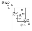
- FIG. 12A is a conceptual diagram of a display device, and FIGS. 12B to 12E are circuit diagrams.
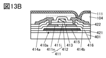
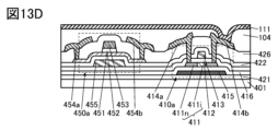
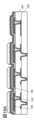
- 13A to 13D are cross-sectional views of transistors.
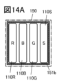
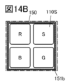
- 14A to 14C are top views of the pixel portion
- FIG. 14D is a circuit diagram.
- 15A to 15C are cross-sectional views for explaining the manufacturing method.
- 16A to 16C are cross-sectional views for explaining the manufacturing method.
- 17A to 17C are cross-sectional views for explaining the manufacturing method.
- 18A to 18C are cross-sectional views for explaining the manufacturing method.
- FIG. 19 is a cross-sectional view for explaining the manufacturing method.
- 20A to 20C are cross-sectional views explaining the manufacturing method.
- FIG. 21 is a cross-sectional view for explaining the manufacturing method.
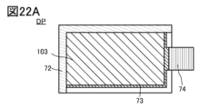
- 22A is a top view of the display device, and FIGS. 22B and 22C are perspective views of the display device.
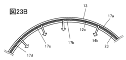
- 23A and 23B are cross-sectional views of the display device.
- 24A and 24B are cross-sectional views of the display device.
- 25A and 25B are perspective views of the display device.
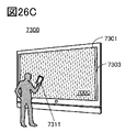
- 26A to 26D are diagrams of electronic equipment.
- 27A and 27B are diagrams of electronic equipment.
- the terms “source” and “drain” of a transistor are interchanged depending on the polarity of the transistor and the level of the potential applied to each terminal.
- a terminal to which a low potential is applied is called a source
- a terminal to which a high potential is applied is called a drain
- a terminal to which a high potential is applied is called a source.
- the terms source and drain may be interchanged depending on the potential relationship, but in this specification and the like, when describing the connection relationship between transistors, the terms source and drain are fixed for convenience.
- a source of a transistor means a source region which is part of a semiconductor layer functioning as an active layer, or a source electrode connected to the source region.
- the drain of a transistor means a drain region that is part of the semiconductor film or a drain electrode connected to the drain region.
- a gate of a transistor means a gate electrode.
- a state in which transistors are connected in series means, for example, a state in which only one of the source and drain of a first transistor is connected to only one of the source and drain of a second transistor.
- a state in which transistors are connected in parallel means that one of the source and drain of the first transistor is connected to one of the source and drain of the second transistor, and the other of the source and drain of the first transistor is connected to It means the state of being connected to the other of the source and the drain of the second transistor.
- connection may be referred to as electrical connection, and includes a state in which current, voltage, or potential can be supplied, or a state in which current, voltage, or potential can be transmitted. Therefore, it also includes a state in which they are connected to each other through elements such as wiring, resistors, diodes, and transistors.
- the electrical connection includes a state of direct connection without an element such as a wiring, resistor, diode, or transistor.
- a conductive layer may have multiple functions such as a wiring or an electrode.
- a light-emitting device is sometimes referred to as a light-emitting element.
- a light-emitting device has a structure in which an organic compound layer is sandwiched between a pair of electrodes.
- One of the pair of electrodes is an anode
- the other of the pair of electrodes is a cathode
- the organic compound layer is a laminate of functional layers
- at least one of the functional layers is a light-emitting layer.
- a pair of electrodes may also be referred to as a lower electrode and an upper electrode, with the lower electrode functioning as one of an anode and a cathode, and the upper electrode functioning as the other of the anode and cathode.
- a light-emitting device having an organic compound layer formed using a metal mask (MM) may be referred to as a light-emitting device having a metal mask (MM) structure.
- the metal mask is sometimes referred to as a fine metal mask (FMM, high-definition metal mask) as the opening becomes finer.
- FMM fine metal mask
- a light-emitting device having an organic compound layer formed without using a metal mask or a fine metal mask may be referred to as a light-emitting device having a metal maskless (MML) structure.
- MML metal maskless
- a light-emitting device that emits red, green, blue, and the like may be referred to as a red-light-emitting device, a green-light-emitting device, and a blue-light-emitting device, respectively.
- a full-color display device can be provided by manufacturing a red light-emitting device, a green light-emitting device, and a blue light-emitting device.
- a light-emitting device that emits white light is sometimes referred to as a white light-emitting device.
- a white light-emitting device can provide a full-color display device by combining it with a colored layer (for example, a color filter or a color conversion layer).
- SBS side-by-side
- SBS structures can be used to fabricate red, green, and blue light emitting devices.
- light-emitting devices can be broadly classified into a single structure and a tandem structure.
- a single structure is a structure having one light-emitting unit between a pair of electrodes.
- the light-emitting unit is an organic compound layer including one or more light-emitting layers, and refers to a laminate.
- one light emitting unit should have two or more light emitting layers, and the light emitted from the two or more light emitting layers should satisfy the relation of complementary colors.
- Two or more light-emitting layers may be in contact with each other in a light-emitting unit.
- a white light-emitting device can be obtained by satisfying a complementary color relationship.
- Three or more light-emitting layers may be in contact with each other in a light-emitting unit.
- a tandem structure is a structure having two or more light-emitting units between a pair of electrodes.
- Each of the two or more light-emitting units is an organic compound layer containing one or more light-emitting layers, and refers to a laminate.
- the charge-generating layer has a function of injecting holes into one of the light-emitting units formed in contact with the charge-generating layer when a voltage is applied between the cathode and the anode. It has the function of injecting electrons into the light-emitting unit.
- the tandem structure preferably has a first light-emitting unit, a charge-generating layer, and a second light-emitting unit between a pair of electrodes, and holes are injected into the first light-emitting unit by the charge-generating layer. , electrons are injected into the second light-emitting unit.
- a structure in which white light emission is obtained by combining light from the light-emitting layers of two or more light-emitting units may be employed. Note that the combination of light-emitting layers for obtaining white light emission should satisfy the complementary color relationship, as in the case of the single structure.
- the light emitting device having the SBS structure can consume less power than the white light emitting device. If it is desired to keep power consumption low, it is preferable to use a light-emitting device with an SBS structure.
- the white light emitting device is preferable because the manufacturing process is simpler than that of the SBS structure light emitting device, so that the manufacturing cost can be lowered or the manufacturing yield can be increased.
- the emissive layer comprises emissive material, which may be fluorescent or phosphorescent.
- the display panel substrate is attached with a connector such as FPC (Flexible Printed Circuit) or TCP (Tape Carrier Package), or an IC is mounted on the substrate by the COG (Chip On Glass) method, etc.
- a module may be referred to as a display module.
- a display module is one aspect of a display device.
- a display device of one embodiment of the present invention includes an auxiliary wiring.
- the auxiliary wiring refers to a layer having an auxiliary function of the main electrode, and the auxiliary function includes, for example, a function of suppressing voltage drop caused by the main electrode.
- the main electrode include a pair of electrodes of a light-emitting device. Since the pair of electrodes functions as the cathode or anode of the light-emitting device, a conductive material having a work function suitable for the cathode or the anode is used. can be expensive. Therefore, in the display device of one embodiment of the present invention, one of the pair of electrodes is electrically connected to an auxiliary wiring to sufficiently suppress the voltage drop.
- the resistivity of the conductive material of the auxiliary wiring is lower than that of the conductive material of the main electrode.
- One of the pair of electrodes for example the upper electrode, can be a continuous layer without being cut off between the plurality of light emitting devices.
- a series of layers may be referred to as a common layer, and a series of electrodes may be referred to as a common electrode.
- the area of the common electrode increases as the size of the display device increases, and voltage drop is likely to occur. Therefore, in the display device of one embodiment of the present invention, one of the pair of electrodes is electrically connected to an auxiliary wiring to sufficiently suppress the voltage drop.
- auxiliary wiring may be referred to as an auxiliary electrode according to its shape, but in this specification and the like, the auxiliary wiring will be used to describe any shape.
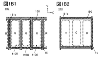
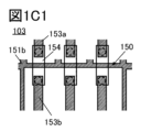
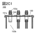
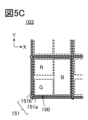
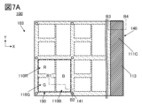
- FIG. 1A shows a conceptual diagram of a pixel portion 103 included in a display device which is one embodiment of the present invention.
- the pixel section 103 has a light emitting device 11W and color filters 148 (148R, 148G, and 148B are used in the drawing).
- the light-emitting device 11W has at least a structure in which a lower electrode 111, an organic compound layer 112, and an upper electrode 113 are laminated in this order.
- the organic compound layer 112 has at least two light-emitting layers. More preferably, in addition to the organic compound layer 112, the light-emitting device 11W is provided with a charge generation layer 531 positioned between the light-emitting layers.
- the charge generation layer 531 is shown in dashed lines in FIG. 1A.
- a light-emitting layer is a layer that includes a light-emitting material (also referred to as a light-emitting substance), and each light-emitting layer can have one or more light-emitting substances.
- the light-emitting device 11W may have functional layers other than the light-emitting layer as organic compound layers. The light-emitting layer and functional layers other than the light-emitting layer will be described later.
- all the organic compound layers 112 including the light-emitting layer can be shared by each light-emitting device.
- An organic compound layer shared by light-emitting devices may be referred to as a common layer.
- a mask is used to define a formation region of the common layer, and the mask is called an area mask or a rough metal mask.
- a white light emitting device can be formed by vapor deposition or the like using the area mask or rough metal mask for all organic compound layers including the light emitting layer.
- Such a white light-emitting device can be manufactured by a simpler manufacturing process than a light-emitting device having an SBS structure in which light-emitting layers are separately formed, so that the manufacturing cost can be reduced or the manufacturing yield can be increased.
- a tandem structure can be used for the organic compound layer for obtaining a white light emitting device.
- the tandem structure preferably has two or more light-emitting units, and it is preferable that the charge-generating layer is positioned between the light-emitting units, and each light-emitting unit may have one or more light-emitting layers.
- the light-emitting unit has two light-emitting layers, the color emitted from the first light-emitting material in the first light-emitting layer is different from the color emitted from the second light-emitting material in the second light-emitting layer. and a white light emitting device having a tandem structure can be obtained.
- a single structure light emitting device may be used to obtain a white light emitting device.
- the single structure only needs to have two or more light-emitting layers in one light-emitting unit, and does not require a charge-generating layer.
- the color emitted from the first light-emitting material of the first light-emitting layer can be different from the color emitted from the second light-emitting material of the second light-emitting layer. and a white light emitting device with a single structure can be obtained.
- white light emitting devices have common layers.
- the white light emitting device may have a configuration in which the common layer is not included and the organic compound layer corresponding to the common layer is separated.
- a lithography method or the like may be used for the division.
- a photolithographic method can be used as the lithographic method.
- Photolithography is a method of exposing a photosensitive material to a desired pattern and forming a pattern from exposed and unexposed areas. Reduction exposure by a stepper can be used for exposure.
- the end faces of the organic compound layer 112 processed by photolithography are often vertical or substantially perpendicular to the formation surface of the substrate or the like, and the taper angle of the end faces of the organic compound layer 112 is 45 degrees or more and 90 degrees. can meet less than That is, the contour of the organic compound layer 112 does not widen. Since the organic compound layer 112 is a laminate, the taper angle can be regarded as an angle formed by a line passing from the upper end of the uppermost layer to the lower end of the lowermost layer of the laminate and the formation surface. In this specification and the like, an end face includes a side face in a cross-sectional view, and can be described as satisfying a taper angle of 45 degrees or more and less than 90 degrees.
- the taper angle refers to the inclination angle formed by the side surface and the bottom surface of the target layer when the target layer is observed in a direction perpendicular to a cross section (for example, a plane perpendicular to the surface of the substrate). . If the bottom surface is unclear, the surface of the substrate can be used to define the tilt angle.
- the distance between the organic compound layers 112 processed by photolithography can be 5 ⁇ m or less, 1 ⁇ m or less, 500 nm or less, 200 nm or less, 100 nm or less, or further 50 nm or less. Since the organic compound layer is a laminate, the above interval can also be regarded as the interval between the lower ends of the lowermost layers of the laminate.
- a common layer can be used in a white light-emitting device, it is better to use a light-emitting device having an organic compound layer separated by photolithography. This is because the distance between organic compounds can be minimized.
- a method for manufacturing a light-emitting device including a photolithography method and the like will be described later.
- a light-emitting device having organic compound layers separated by photolithography is called a light-emitting device having an MML structure. If the MML structure is applied, it becomes possible to electrically connect the common electrode and the auxiliary wiring at any position. Specifically, a contact hole for electrically connecting the common electrode and the auxiliary wiring can also be provided between the white light emitting devices. Further, the voltage drop can be effectively suppressed by the auxiliary wiring.
- a color filter method can be employed to make the white light emitting device full color.
- the above-described color filters 148 (148R, 148G, and 148B are used in the drawing) are arranged so as to overlap the light emitting device 11W.
- a configuration including the color filter 148 and the light emitting device 11W is sometimes referred to as a sub-pixel 110 (110R, 110G, and 110B are used in the figure).
- the color filters 148 include a red color filter 148R that transmits light in the red wavelength range, a green color filter 148G that transmits light in the green wavelength range, and a blue color filter that transmits light in the blue wavelength range.
- Filter 148B is used.
- Each light emitting device can emit red, green, and blue colors in the direction of the arrows through color filters 148 .
- a color filter can be called a colored layer that transmits light in a specific wavelength range. Transmitting light in a specific wavelength range means that light transmitted through a color filter has at least a wavelength peak corresponding to a specific color.
- the color filters can be formed at desired positions using various materials such as chromatic translucent resins by a printing method, an inkjet method, an etching method using a photolithography method, or the like.
- Photosensitive and non-photosensitive organic resins can be used as the chromatic light-transmitting resin, but if a photosensitive organic resin is used, the number of resist masks used for the etching can be reduced. , which simplifies the process and is preferable.
- Chromatic colors are colors other than achromatic colors such as black, gray, and white. Specifically, red, green, blue, and the like can be used. Cyan, magenta, yellow, or the like may be used as the color of the color filter.
- the film thickness of the color filter can be 500 nm or more and 5 ⁇ m or less.
- Using a color filter can eliminate the need for an optical element such as a circularly polarizing plate or a polarizing plate. Since the optical element is not required, the weight and thickness of the display device can be reduced, which is preferable.
- the upper electrode 113 of each light emitting device is divided in each light emitting device.
- FIG. 1A shows a segmented top electrode.
- the upper electrode may be provided as a continuous electrode, that is, as a common electrode, without being separated for each light emitting device.
- the upper electrode is used as the main electrode, and the auxiliary wiring 151 is electrically connected to the upper electrode. This state is indicated by a solid line in FIG. 1A following the circuit diagram. Voltage drop is sufficiently suppressed in the upper electrode 113 electrically connected to the auxiliary wiring 151 .
- the auxiliary wiring 151 of one embodiment of the present invention has two or more wiring layers provided in different layers.
- the auxiliary wiring 151 has, for example, a first wiring layer 151a and a second wiring layer 151b as shown in FIG. 1A.
- the first wiring layer 151a is formed in a layer different from the second wiring layer 151b, and the surface on which the first wiring layer 151a is formed is the same as the surface on which the second wiring layer 151b is formed. different.
- Wiring layers having different formation surfaces are referred to as wiring layers provided in different layers.
- a wiring layer may be referred to as an electrode layer according to its shape, but in this specification and the like, the wiring layer will be used regardless of the shape.
- the contact holes 15 in the insulating layer 14 located between the first wiring layer 151a and the second wiring layer 151b are interposed.
- the first wiring layer 151a is electrically connected to the second wiring layer 151b.
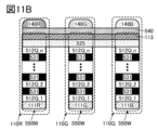
- auxiliary wiring a multi-layered wiring layer of three or more layers such as the first wiring layer to the third wiring layer may be provided.
- a multi-layered wiring layer As the number of laminations increases, it becomes easier to arrange auxiliary wiring (hereinafter sometimes referred to as layout).
- layout auxiliary wiring
- one of the multilayered wiring layers can be laid out in a layer different from the lower electrode.
- one of the wiring layers can have a region overlapping with the lower electrode, and a wider area than the conventional auxiliary wiring can be secured.
- the auxiliary wiring having such a wiring layer is preferable because it can sufficiently suppress the voltage drop.
- a multi-layered wiring layer is preferable because it has no layout restrictions and can sufficiently suppress a voltage drop.
- the second wiring layer 151b can be formed in a grid pattern when viewed from above. Also, the first wiring layer 151a can be formed in a grid pattern when viewed from above, similarly to the second wiring layer 151b.
- the auxiliary wiring 151 of one embodiment of the present invention is characterized by having multiple wiring layers, specifically, having two or more wiring layers provided in different layers. Wiring layers located in different layers are electrically connected to each other through contact holes and can function as auxiliary wiring 151 . Multilayered wiring layers have less restrictions on layout, and thus are suitable for auxiliary wiring.
- a contact hole is an opening formed in an insulating layer, and a wiring layer positioned below the insulating layer (referred to as a lower wiring layer) is connected to a wiring layer positioned above the insulating layer (referred to as an upper wiring layer). allows electrical connection with For electrical connection, the lower wiring layer has a region exposed through the opening, and the upper wiring layer has a region located inside the opening in cross-sectional view.
- the insulating layer provided with the contact hole may have a stacked-layer structure (referred to as a stacked insulating layer).
- a stacked insulating layer For example, when a contact hole is formed in a laminated insulating layer in which a first insulating layer and a second insulating layer are laminated, the first contact hole is formed in the first insulating layer and the second insulating layer is formed in the second insulating layer. 2 contact holes are formed. At this time, if the first contact hole has at least a region overlapping with the second contact hole, the lower wiring layer can be electrically connected to the upper wiring layer.
- the width of the second contact hole in a cross-sectional view is preferably larger than the width of the first contact hole, but the lower wiring layer is the upper wiring layer.
- the width of the contact hole in each insulating layer is not limited as long as it can be electrically connected to the layer.
- the auxiliary wiring 151 of one embodiment of the present invention includes the first wiring layer 151a and the second wiring layer 151b, one of the first wiring layer and the second wiring layer is located in the same layer as the lower electrode. However, the other of the first wiring layer and the second wiring layer is positioned in a different layer from the lower electrode, and the auxiliary wiring 151 can be laid out without being affected by the layout of the lower electrode. In the high-density pixel portion, the spacing between the lower electrodes becomes narrow, and the layout of the auxiliary wiring may become difficult. 151 can sufficiently suppress the voltage drop of the upper electrode.
- both the first wiring layer 151a and the second wiring layer 151b should be formed in layers different from the lower electrodes.
- the second wiring layer 151b is positioned above the first wiring layer 151a and has the same conductive layer as the lower electrode, in order to reduce the influence of the layout of the lower electrode, the 2 wiring layers 151b are formed in a small area, and the first wiring layers 151a electrically connected to the second wiring layers 151b are laid out. Since the first wiring layer 151a is located in a layer different from that of the lower electrode, the degree of layout freedom is high, which is preferable.
- the auxiliary wiring 151 of one embodiment of the present invention can be laid out without being affected by the layout of the lower electrode.
- the first wiring layer 151a and the second wiring layer 151b provided in different layers can have different top-view shapes.
- the second wiring layer 151b can be grid-shaped, and the first wiring layer 151a can be strip-shaped.
- the first wiring layer 151a can be formed in a grid shape, and the second wiring layer 151b can be formed in a band shape.
- a grid is a pattern that combines a plurality of parallel vertical lines and a plurality of parallel horizontal lines.
- a belt shape may be called a rectangular shape or a stripe shape.
- FIGS. 1B1 and 1B2 show top views of the pixel portion 103, and both show how the second wiring layer 151b has a grid pattern.
- the first wiring layer 151a is electrically connected to the second wiring layer 151b through the contact hole 15 (not shown).
- the first wiring layer 151a may have a strip shape, and is preferably laid out in a region overlapping with a part of the second wiring layer 151b.
- the first wiring layer 151a is not limited to a strip shape, and may have any shape.
- 1B1 and 1B2 are attached with an X direction and a Y direction that intersects with the X direction, and the layout of the configuration of the pixel portion 103 and the like are sometimes described using these directions.
- the second wiring layer 151b shown in FIG. 1B1 has a grid shape with a plurality of vertical lines having regions overlapping the gaps between subpixels.
- the sub-pixel gap is the area between the edge of the lower electrode 111 of the sub-pixel 110R and the edge of the lower electrode 111 of the sub-pixel 110G, and the edge of the lower electrode 111 of the sub-pixel 110G and the lower electrode 111 of the sub-pixel 110B. has an area between the ends of
- the gap of the pixel 150 has, for example, an area between the edge of the lower electrode 111 of the sub-pixel 110B located at the edge of the pixel 150 and the edge of the lower electrode 111 of the sub-pixel 110R located at the edge of the adjacent pixel.
- "Adjacent" may mean either a relationship of being adjacent along the X direction or a relationship of being adjacent along the Y direction.
- the second wiring layer 151b shown in FIG. 1B2 does not have a plurality of vertical lines having regions overlapping sub-pixel gaps as shown in FIG. 1B1.
- the wiring having the above function needs to extend in the X direction or the Y direction, it short-circuits with the grid-shaped second wiring layer 151b. Therefore, when the grid-like second wiring layer is provided as an auxiliary wiring, it is better not to provide wiring having functions such as scanning lines, signal lines, and power supply lines in the same layer as the second wiring layer. If scanning lines, signal lines and power supply lines are to be provided, the lengths of the scanning lines, signal lines and power supply lines in the X direction or the Y axis direction should be adjusted so as not to short-circuit with the second wiring layer. Layout should be done.
- bridge wiring When the length in the X-direction or the length in the Y-axis direction is adjusted, electrical connection is ensured in a conductive layer different from the second wiring layer. Wiring for ensuring such electrical connection is sometimes referred to as bridge wiring.
- the bridge wiring may be referred to as a bridge electrode depending on its shape, but in this specification and the like, the bridge wiring will be used for explanation.
- FIGS. 1C1 and 1C2 show a pixel portion 103 having signal lines and bridge wirings. Although illustration of the light emitting device 11W is omitted in FIGS. 1C1 and 1C2, FIGS. 1B1 and 1B2 can be referred to for the layout and the like of the light emitting device 11W.
- the signal line shown in FIGS. 1C1 and 1C2 has a third wiring layer 153a and a fourth wiring layer 153b, and the third wiring layer 153a is separated from the fourth wiring layer 153b. Therefore, the bridge wiring 154 is used to electrically connect the third wiring layer 153a and the fourth wiring layer 153b.
- the third wiring layer 153a and the fourth wiring layer 153b have the same conductive layer as the second wiring layer 151b.
- the bridge wiring 154 has a conductive layer different from the second wiring layer 151b, and preferably uses a conductive layer lower than the second wiring layer 151b.
- the gap between the lower electrodes becomes narrower, making it difficult to lay out auxiliary wiring in the gap between the lower electrodes.
- the gap between the lower electrodes is, for example, the distance between the edge of the lower electrode 111 of the subpixel 110R and the edge of the lower electrode 111 of the subpixel 110G, or the edge of the lower electrode 111 of the subpixel 110G and the edge of the lower electrode 111 of the pixel 110B. is the distance between Therefore, when the second wiring layer 151b is located in the same layer as the lower electrode 111, the layout of the second wiring layer as shown in FIG. 1B2 is preferable in a display device with high definition.
- the layout of the second wiring layer as shown in FIG. 1B2 is preferable because it facilitates the layout of each conductive layer even in the pixel portion 103 having signal lines and bridge wirings as shown in FIG. 1C2.
- FIG. 2A shows another mode of the pixel portion 103 of one embodiment of the present invention.
- 2A has a configuration in which the second wiring layer 151b and the lower electrode 111 are located on the same formation surface. Note that the same forming surface corresponds to the upper surface of the insulating layer 14 .
- Other configurations can be the same as in FIG. 1A.
- 2B1 and 2B2 show top views of the pixel portion 103, and both show how the first wiring layer 151a has a grid pattern.
- For the grid-like layout refer to the layout of the grid-like second wiring layer 151b shown in FIGS. 1B1 and 1B2.
- the second wiring layer 151b is positioned so as to overlap the intersections of the grid-like first wiring layer 151a.
- the second wiring layer 151b only needs to overlap the intersections, and does not have to overlap the entire side of the grid-like first wiring layer 151a.
- the second wiring layer 151b does not have to overlap with all intersections of the grid-like first wiring layer 151a. Since the second wiring layer 151b has the same conductive layer as the lower electrode 111, the second wiring layer 151b must be laid out so as not to be in contact with the lower electrode 111, but since it has the first wiring layer 151a, Voltage drop can be sufficiently suppressed.
- the second wiring layer 151b laid out in a small area may be preferably referred to as an electrode layer.
- FIGS. 2C1 and 2C2 show the pixel portion 103 having signal lines and bridge wirings.
- the signal line shown in FIGS. 2C1 and 2C2 has a third wiring layer 153a and a fourth wiring layer 153b, and the third wiring layer 153a is separated from the fourth wiring layer 153b. Therefore, the bridge wiring 154 is used to electrically connect the third wiring layer 153a and the fourth wiring layer 153b.
- the third wiring layer 153a and the fourth wiring layer 153b have the same conductive layer as the first wiring layer 151a.
- the bridge wiring 154 has a conductive layer different from the first wiring layer 151a, preferably a conductive layer lower than the first wiring layer 151a.
- the bridge wiring 154 may use the same conductive layer as the second wiring layer 151b. In this case, the layout is made so that the lower electrode 111 and the bridge wiring 154 are not in contact with each other.
- FIG. 3A shows another mode of the pixel portion 103 of one embodiment of the present invention.
- 3A differs from FIG. 2A in that the width of the second wiring layer 151b (the width in dB) in cross section is smaller than the width of the first wiring layer 151a (the width in dA).
- Other configurations can be the same as in FIG. 2A.
- FIG. 3B shows a top view of the pixel portion 103, showing how the first wiring layer 151a and the second wiring layer 151b have a grid pattern.
- For the grid-like layout refer to the layout of the grid-like second wiring layer 151b shown in FIG. 1B2.
- the contact hole 15 shown in FIG. 3B can have a shape that matches the region where the first wiring layer 151a and the second wiring layer 151b overlap.
- contact hole 15 can have a shape along one side of second wiring layer 151b.
- FIG. 3C shows a pixel portion 103 having signal lines and bridge lines.
- the signal line shown in FIG. 3C has a third wiring layer 153a and a fourth wiring layer 153b, and the third wiring layer 153a is separated from the fourth wiring layer 153b. Therefore, the bridge wiring 154 is used to electrically connect the third wiring layer 153a and the fourth wiring layer 153b.
- the third wiring layer 153a and the fourth wiring layer 153b have the same conductive layer as the first wiring layer 151a.
- the bridge wiring 154 has a conductive layer different from the first wiring layer 151a, preferably a conductive layer lower than the first wiring layer 151a.
- the auxiliary wiring 151 of one embodiment of the present invention has two or more wiring layers provided in different layers, the degree of freedom in layout of the auxiliary wiring 151 is higher than in the case where the auxiliary wiring is formed from one wiring layer. is highly desirable.
- the auxiliary wiring 151 of one embodiment of the present invention can also be applied to a high-definition display device.
- the conductive material included in the auxiliary wiring 151 of one embodiment of the present invention that is, the conductive material included in the first wiring layer 151a or the second wiring layer 151b include aluminum, copper, silver, gold, platinum, chromium, molybdenum, and the like. of metals can be used. An alloy of the above metals can be used as the conductive material.
- the conductive material is a metal and a non-translucent conductive material.
- the first wiring layer 151a or the second wiring layer 151b can be formed as a single layer or a stacked layer using the above conductive material.
- the first wiring layer 151a may be laminated and the second wiring layer 151b may be formed as a single layer.
- the first wiring layer 151a may be a single layer and the second wiring layer 151b may be a laminated layer.
- the first wiring layer 151a may be laminated, and the second wiring layer 151b may also be laminated.
- a conductive material having a light-transmitting property may be used as the conductive material included in the auxiliary wiring of one embodiment of the present invention, that is, the conductive material included in the first wiring layer 151a or the second wiring layer 151b.
- an oxide containing indium and tin also referred to as indium tin oxide, In—Sn oxide, or ITO
- an oxide containing indium, silicon, and tin oxide containing indium, silicon, and tin
- In—Si—Sn oxide, ITSO oxide containing indium and zinc also called indium zinc oxide or In--Zn oxide
- oxide containing indium, tungsten, and zinc also called In--W--Zn oxide
- the first wiring layer 151a or the second wiring layer 151b can be formed as a single layer or a stacked layer using the above conductive material.
- the resistivity of the conductive material used for the auxiliary wiring of one embodiment of the present invention is the same as the conductivity used for the common electrode. It is preferably lower than the resistivity of the material. However, if the voltage drop caused by the common electrode can be sufficiently suppressed, the above relationship of resistivity need not be satisfied.
- a display device of one embodiment of the present invention preferably has a top emission structure.
- the upper electrode In the top emission structure, the upper electrode must be translucent, and light is emitted in the direction of the upper electrode. Translucency refers to the passage of visible light (light with a wavelength of 400 nm or more and less than 750 nm), and preferably has a transmittance of 40% or more.
- the upper electrode may be read as a common electrode.
- a light-transmitting conductive material may have high resistivity, which may increase the resistance of the common electrode. Then, a voltage drop occurs due to the common electrode, the potential distribution in the display surface becomes non-uniform, and the brightness of the light-emitting device varies. Therefore, the display device having the top emission structure of one embodiment of the present invention may include auxiliary wirings electrically connected to the common electrode. The auxiliary wiring can have an effect of suppressing a voltage drop.
- auxiliary wiring electrically connected to the common electrode.
- the auxiliary wiring can have an effect of suppressing a voltage drop.
- the lower electrode In the bottom emission structure, the lower electrode must be translucent, and light is emitted in the direction of the lower electrode. Furthermore, it is necessary to arrange a color filter on the lower electrode side.
- FIG. 4A shows the pixel portion 103 included in the display device with the top emission structure, and the cross-sectional structure of the auxiliary wiring 151 and the like provided in the pixel portion 103 will be described.
- the cross-sectional structure of the auxiliary wiring 151 described in FIG. 3 and the like in the above embodiment mode is applied.
- the cross-sectional structure of the auxiliary wiring 151 may be applied.
- the pixel portion 103 has a light emitting device 11W.
- the light emitting device 11W is a white light emitting device, but has the organic compound layer 112 which is separated.
- the organic compound layer 112 has the same light-emitting material.
- the light emitting device 11W has a common electrode 113. As shown in FIG. Since the common electrode 113 has translucency, light is emitted from each light emitting device in the direction of the arrow.
- the light emitting device 11W is formed on the insulating layer 104, and the insulating layer 104 is formed on the substrate 101.
- the auxiliary wiring 151 of one embodiment of the present invention has two or more wiring layers provided in different layers, for example, a first wiring layer 151a and a second wiring layer 151b as shown in FIG. 4A.
- a first wiring layer 151a formed on the substrate 101 and a second wiring layer 151b formed on the insulating layer 104 are used in FIG. 4A. show.
- the common electrode 113 is located on the insulating layer 126 and can be electrically connected to the auxiliary wiring 151 through the contact hole 18 of the insulating layer 126 . Further, the second wiring layer 151b is electrically connected to the first wiring layer 151a through the contact hole 19 of the insulating layer 104 and functions as the auxiliary wiring 151.
- FIG. 1 A first wiring layer 151a through the contact hole 19 of the insulating layer 104 and functions as the auxiliary wiring 151.
- the auxiliary wiring 151 has two or more wiring layers provided in different layers, even if any one of the wiring layers is provided on the same formation surface as the lower electrode formation surface, the influence of the layout of the lower electrode does not occur. It is preferable that the auxiliary wiring 151 can be laid out without being influenced by the layout of the lower electrode or by minimizing the influence of the layout of the lower electrode.
- the second wiring layer 151b is provided in the same layer as the lower electrode 111.
- the first wiring layer 151a is provided in a layer different from that of the lower electrode 111, it can be laid out in a larger area than the second wiring layer 151b. Since the display device has a top emission structure, the aperture ratio does not decrease even if the first wiring layer 151a overlaps with the light emitting device. Therefore, a conductive material with low resistivity can be used for the first wiring layer 151a.
- the voltage drop in the common electrode 113 can be sufficiently suppressed by the auxiliary wiring 151 of one embodiment of the present invention.
- a wiring layer included in the auxiliary wiring 151 may be provided in a layer different from that of the lower electrode.
- the auxiliary wiring 151 of one embodiment of the present invention can include a wiring layer having a formation surface different from the formation surface of the lower electrode, and the wiring layer is not affected by the lower electrode layout. It can be formed over a wide area, and the voltage drop suppressing effect can be fully exhibited.
- FIG. 4B includes an X direction and a Y direction that intersects with the X direction, and the layout and the like of the configuration of the pixel portion 103 may be described using these directions.
- the pixel portion 103 located in the display area has a plurality of pixels 150 .
- a protection circuit or the like may be provided in the display region.
- a pixel 150 is used as a minimum unit capable of full-color display, and has at least a sub-pixel 110R, a sub-pixel 110G, and a sub-pixel 110B as shown in FIG. 4B. Note that each of the sub-pixel 110R, the sub-pixel 110G, and the sub-pixel 110B has a color filter for full-color display.
- the sub-pixel 110 When describing items common to the sub-pixel 110R, the sub-pixel 110G, and the sub-pixel 110B, the sub-pixel 110 may be referred to.
- Sub-pixel 110R, sub-pixel 110G, and sub-pixel 110B correspond to light-emitting regions of each light-emitting device, and each light-emitting region is illustrated as being rectangular in FIG. 4B.
- the sub-pixel 110R corresponds to the light-emitting region (illustrated as R) that has passed through the red color filter
- the sub-pixel 110G corresponds to the light-emitting region (illustrated as G) that has passed through the green color filter
- the sub-pixel 110B corresponds to the light-emitting region (shown as B) that has passed through the blue color filter.
- the display device of one embodiment of the present invention is not limited to the above emission colors, and a white light-emitting region may be provided without color filters.
- the sub-pixels 110R and 110G are alternately laid out along the Y direction, and the sub-pixels 110B are arranged along the Y direction.
- Sub-pixel 110B can have a larger area than sub-pixel 110R and sub-pixel 110G.
- an insulating layer 104 is provided on a substrate 101, and a sub-pixel 110R includes a lower electrode 111 on the insulating layer 104, an organic compound layer 112 on the lower electrode 111, and an organic compound layer 112 on the lower electrode 111. It has a common electrode 113 on layer 112 .
- the light emitting device 11W of the sub-pixel 110R can emit light in the direction indicated by the arrow through the color filter 148R located on the common electrode 113 side.
- the sub-pixel 110G and the sub-pixel 110B have the same configuration as the sub-pixel 110R.
- the light emitting device 11W of the sub-pixel 110G can emit light in the direction indicated by the arrow through the color filter 148G located on the common electrode 113 side.
- the light emitting device 11W of the sub-pixel 110B can emit light in the direction indicated by the arrow through the color filter 148B located on the common electrode 113 side.
- the sub-pixel 110 may have a switching element for controlling the light emitting device in addition to the light emitting device.
- switching elements are not shown in FIGS. 4A and 4B.
- a display device of one embodiment of the present invention can perform display by emitting light from a light-emitting device controlled by a switching element.
- the auxiliary wiring 151 is formed using a conductive layer provided in the same layer as the lower electrode 111 as the second wiring layer 151b.
- the auxiliary wiring 151 has a first wiring layer 151 a, which is a wiring layer provided in a layer different from the lower electrode 111 .
- the second wiring layer 151b since the second wiring layer 151b has a wiring layer on the same formation surface as the lower electrode, it is provided in a region not in contact with the lower electrode 111, that is, in a region not overlapping the sub-pixels. As a result, for example, the second wiring layer 151b has a lattice shape when viewed from above.
- the second wiring layer 151b has regions extending along the X direction as horizontal lines, the regions being parallel to each other, and regions extending along the Y direction as vertical lines. are in parallel.
- the second wiring layer 151b shown in FIG. 4B has a region located between the sub-pixel 110R and the sub-pixel 110G as a region extending along the X direction, and the regions are arranged in parallel. .
- a region located between the sub-pixel 110R and the sub-pixel 110G corresponds to a region between pixels.
- the second wiring layer 151b shown in FIG. 4B has a region located between the sub-pixel 110G and the sub-pixel 110B as a region extending along the Y direction, and the regions are arranged in parallel.
- the gap between the lower electrodes 111 becomes narrower in a display device with higher definition.
- the distance de between sub-pixels and the distance dc between pixels are narrow. It becomes difficult to form a wiring layer for auxiliary wiring in a narrow area. Therefore, in the auxiliary wiring 151 which is one embodiment of the present invention, the second wiring layer 151b is preferably provided at least in the gap between subpixels between pixels. Further, as the wiring layer provided in the gap between the sub-pixels, it is preferable to use a wiring layer of a layer different from that of the lower electrode, such as the first wiring layer 151a.
- an insulating layer 126 is preferably located between the light-emitting devices as shown in FIG. 4A.
- the insulating layer 126 can fill between pixels and between subpixels, and the second wiring layer 151b is positioned so as to overlap with the insulating layer 126, which is one of the structures that can provide a high-definition display device. do it.
- the insulating layer 126 can prevent the second wiring layer 151 b from contacting the lower electrode 111 .
- the insulating layer 126 can reliably separate or separate the organic compound layers 112, and can suppress crosstalk between the light emitting devices.
- the top surface of insulating layer 126 is shown to be generally coincident or coincident with the top surface of organic compound layer 112 .
- the surface on which the common electrode 113 is formed becomes flat, and the common electrode 113 is less likely to be cut, which is preferable.
- the top surface of the insulating layer 126 may be positioned above the top surface of the organic compound layer 112 so that the common electrode 113 is not cut.
- the end portion of the insulating layer 126 is preferably thinned gradually toward the organic compound layer 112 .
- a shape that gradually becomes thinner is sometimes referred to as a taper.
- the central portion of the insulating layer 126 is located above the edge portions of the insulating layer 126 and that the central portion has a region that rises above the edge portions. Providing the common electrode 113 on such an insulating layer 126 is preferable because the common electrode 113 is less likely to be cut.
- the second wiring layer 151b of the auxiliary wiring 151 has a region in contact with the bottom of the common electrode 113.
- the auxiliary wiring 151 should be electrically connected to the common electrode 113. It is sufficient if a proper connection can be secured.
- a top emission structure is preferably applied to the display device of one embodiment of the present invention.
- the common electrode 113 has a high visible light transmittance, and for example, a transmittance of 40% or more is preferable.
- the auxiliary wiring 151 of one embodiment of the present invention is characterized by having at least two wiring layers.
- a specific layout example of the first wiring layer 151a and the second wiring layer 151b will be described with reference to FIG. 5 and the like. 5 and the like show the sub-pixels (R, G, B) according to FIG. 4B, but the lower electrode 111 is omitted in order to show a layout example of the first wiring layer 151a and the second wiring layer 151b.
- the auxiliary wiring 151 has a lattice shape when viewed from above, and has a first wiring layer 151a extending in the Y direction and a second wiring layer 151b extending in the X direction.
- a contact hole is located in a region where the first wiring layer 151a and the second wiring layer 151b intersect, but it is not shown in FIG. 5A.
- Either the first wiring layer 151a or the second wiring layer 151b may be formed in the same layer as the lower electrode 111, or both may be formed in different layers from the lower electrode 111.
- FIG. 1 Either the first wiring layer 151a or the second wiring layer 151b may be formed in the same layer as the lower electrode 111, or both may be formed in different layers from the lower electrode 111.
- both the first wiring layer 151a and the second wiring layer 151b are located between the pixels.
- the pixel portion 103 is used for a high-definition display device.
- FIG. 5B shows an auxiliary wiring 151 having a small length in the second wiring layer 151b shown in FIG. 5A. Since the second wiring layer 151b is short, the first wiring layer 151a has a region extending in the X direction. The second wiring layer 151b has such a length that one end overlaps the sub-pixel 110G and the other end overlaps the sub-pixel 110B. Other configurations are the same as those in FIG. 5A.
- FIG. 5C shows an auxiliary wiring 151 having the first wiring layer 151a shown in FIG. 5A as the second wiring layer 151b and the second wiring layer 151b shown in FIG. 5A as the first wiring layer 151a.
- Other configurations are the same as those in FIG. 5A.
- FIG. 5D shows the auxiliary wiring 151 having a small length of the first wiring layer 151a shown in FIG. 5C. Since the length of the first wiring layer 151a is short, the second wiring layer 151b has a region extending in the X direction. The short first wiring layer 151a has such a length that one end overlaps the sub-pixel 110G and the other end overlaps the sub-pixel 110B. Other configurations are the same as in FIG. 5C.
- FIG. 5A shows the auxiliary wiring 151 in which the first wiring layer 151a and the second wiring layer 151b have the same shape.
- the first wiring layer 151a is indicated by a dotted line.
- Other configurations are the same as those in FIG. 5A.
- FIG. 6B shows the auxiliary wiring 151 having the first wiring layer 151a having a larger area than the second wiring layer 151b.
- a wiring layer functioning as an auxiliary wiring preferably has a large area. Since it is formed in a layer different from that of the lower electrode 111, the first wiring layer 151a can be formed with a large area.
- An opening 152 is provided in the first wiring layer 151a to ensure electrical connection between the lower electrode and the transistor.
- Other configurations are the same as those in FIG. 5A.
- the auxiliary wiring 151 of one embodiment of the present invention has the first wiring layer 151a and the second wiring layer 151b, it can take various forms. By electrically connecting the auxiliary wiring 151 to the common electrode, the voltage drop of the common electrode can be sufficiently suppressed.
- a high-definition pixel portion can be used for the display device of one embodiment of the present invention.
- the auxiliary wiring 151 may be applied to the bottom emission structure.
- the cross-sectional structure of the auxiliary wiring 151 described in FIGS. 1 to 3 and the like in the above embodiment can be applied.
- the first wiring layer 151a provided below the lower electrode 111 has a lattice shape or a lattice shape overlapping with the gaps between the subpixels or the gaps between the pixels. It is preferable to have an area smaller than the shape.
- the second wiring layer 151b provided below the lower electrode 111 preferably has a lattice shape overlapping with the gaps between the sub-pixels or the gaps between the pixels, or has an area smaller than the lattice shape.
- the display device 100 has a pixel portion 103 and a connection portion 140 .
- the pixel portion 103 has a plurality of pixels 150 .
- the pixel 150 has a plurality of sub-pixels 110 (110R, 110G, and 110B are used in the figure), and the regions corresponding to the sub-pixels are also labeled R, G, and B.
- the arrangement of FIG. 7A is similar to the arrangement shown in FIG. 4B, etc., and is a regular arrangement.
- the pixel portion 103 has contact holes 141 .
- the contact hole 141 is selectively provided, and can be provided, for example, in a region corresponding to the outer periphery of the pixel 150, such as the four corners of the pixel 150, for example.
- the light emitting device 11W it is preferable to use an element such as an OLED (Organic Light Emitting Diode) or a QLED (Quantum-dot Light Emitting Diode).
- the light-emitting substances possessed by the light-emitting device include substances that emit fluorescence (fluorescent materials), substances that emit phosphorescence (phosphorescent materials), inorganic compounds (quantum dot materials, etc.), and substances that exhibit heat-activated delayed fluorescence (heat-activated delayed fluorescence (thermally activated delayed fluorescence: TADF) material) and the like.
- connection portion 7A is a region having a connection electrode 111C electrically connected to the common electrode 113.
- the connection portion 140 may be referred to as a cathode contact portion or a cathode contact portion.
- the common electrode 113 preferably extends to the connection portion 140 beyond the edge of the pixel portion 103 .
- the common electrode 113 extending to the connection portion 140 is indicated by a dotted line.
- a potential to be supplied to the common electrode 113 is applied to the connection electrode 111C.
- a voltage drop may occur in the common electrode 113 depending on the distance from the connection portion 140 . If a voltage drop occurs, the value of the potential will vary. Since the display device of this embodiment mode includes the auxiliary wiring 151 at least in the pixel portion 103, the potential value does not vary, which is preferable.
- the auxiliary wiring 151 can be provided in the connection portion 140 in addition to the pixel portion 103 .
- connection electrode 111 ⁇ /b>C can be provided along the outer periphery of the pixel portion 103 .
- the connection electrode 111C may be provided along one side of the periphery of the pixel portion 103, or may be provided over two or more sides of the periphery of the pixel portion 103.
- the auxiliary wiring 151 can have a structure in which a power supply potential or a signal is not directly supplied. That is, the auxiliary wiring 151 can be configured so as not to be connected to wirings or electrodes other than the common electrode 113 . On the other hand, the auxiliary wiring 151 may be supplied with a power supply potential (for example, a cathode potential). As a result, the potential is supplied to the common electrode 113 not only from the connection electrode 111C but also from the auxiliary wiring 151, so that the voltage drop can be suppressed more effectively.
- a power supply potential for example, a cathode potential
- a configuration may be adopted in which a power supply potential is supplied from the auxiliary wiring 151 to the common electrode 113, and the connection electrode 111C, the connection portion 140, and the like are not provided. This makes it possible to reduce the size of the display device.
- 7B and 7C are cross-sectional views corresponding to dashed-dotted lines B1-B2 and dashed-dotted lines B3-B4 in FIG. 7A, respectively.
- the color filter 148G, the color filter 148B, and the light blocking layer 149 are preferably arranged on the substrate 170 side.
- the color filter 148B is formed so as to partially overlap the previously formed color filter 148G.
- the light shielding layer 149 is sometimes called a black matrix, and is arranged in a portion where the color filters overlap each other. That is, the light shielding layer 149 is preferably arranged so as to overlap with the non-light-emitting region.
- a cross-sectional view of the contact hole 141 is also shown in FIG. 7B.
- a contact hole 141 is formed in the insulating layer 126 . Through the contact hole 141, the second wiring layer 151b and the common electrode 113 can be electrically connected.
- the contact hole 141 is a non-light emitting region and preferably overlaps with the light shielding layer 149 .
- the pixel section 103 also has contact holes 142 in the insulating layer 104 .
- the contact hole 142 may be formed in a region that overlaps with the contact hole 141 or may be formed in a region that does not overlap with the contact hole 141 .
- the size (eg width in cross section) of the contact hole 141 is preferably larger than the size (eg width in cross section) of the contact hole 142.
- the end faces of the organic compound layer 112 processed using the photolithography method are vertical or substantially vertical.
- the taper angle of the end surface of the organic compound layer 112 is preferably 45 degrees or more and less than 90 degrees. It is preferable that the taper angle of the end faces of the other organic compound layers also satisfy 45 degrees or more and less than 90 degrees.
- the taper angle can be regarded as an angle formed by a line passing from the upper end of the uppermost layer of the laminate to the lower end of the lowermost layer and the formation surface. Satisfying the above taper angle facilitates fine processing, for example, facilitates the formation of contact holes 141 between light emitting devices.
- the organic compound layer 112 has functional layers that enable a white light emitting device.
- a tandem structure or a single structure can be used to provide a white light emitting device.
- the tandem structure has a charge generation layer 531 .
- the organic compound layer 112 includes, as functional layers other than the light-emitting layer, a substance with a high hole-injection property, a substance with a high hole-transport property, a hole-blocking material, a substance with a high electron-transport property, and a substance with a high electron-injection property. , an electron-blocking material, or a layer containing a bipolar substance (a substance with high electron-transporting and hole-transporting properties), or the like.
- a layer containing a substance with a high hole-injection property is referred to as a hole-injection layer.
- a layer containing a substance having a high hole-transport property is referred to as a hole-transport layer.
- a layer with a hole blocking material is referred to as a hole blocking layer.
- a layer containing a substance having a high electron-transport property is referred to as an electron-transport layer.
- a layer containing a highly electron-injecting substance is referred to as an electron-injecting layer.
- a layer with an electron blocking material is referred to as an electron blocking layer.
- a hole injection layer and an electron injection layer may be referred to as a carrier injection layer.
- Each functional layer can be formed by a vapor deposition method (including a vacuum vapor deposition method), a transfer method, a printing method, an inkjet method, a coating method, or the like.
- the common layer 114 can have one or more selected from an electron injection layer, an electron transport layer, a hole injection layer, and a hole transport layer. Having two or more layers includes combining two or more different functional layers and having two or more layers having the same functional layer but different materials in combination. Specific materials that can be used for the functional layer will be described later.
- the organic compound layer 112 has a laminate of a hole injection layer, a hole transport layer, a light emitting layer, and an electron transport layer in this order from the lower electrode 111 side, and the laminate is a charge generation layer. and the common layer 114 is an electron injection layer included in the upper laminate.
- the functional layer does not necessarily need to contain an organic compound as long as it can exhibit each function.
- a layer containing only an inorganic compound or an inorganic substance can be used for the electron injection layer or the like.
- the lower electrode 111 is provided for each light emitting device. Also, the common electrode 113 and the common layer 114 are provided as a continuous layer common to each light emitting device. A conductive film having a reflective property is used for the lower electrode 111 and a conductive film having a property of transmitting visible light is used for the common electrode 113, so that the display device can have a top-emission structure.
- the end of the lower electrode 111 preferably has a taper.
- the end of the organic compound layer 112 is preferably located in a region beyond the lower electrode 111, and when the end of the lower electrode 111 has a taper, the organic compound layer 112 has a shape along the taper. By tapering the side surface of the lower electrode 111, coverage with an organic compound layer or the like can be improved.
- the lower electrode 111 is an electrode electrically connected to the transistor and is sometimes referred to as a pixel electrode. Also, since the lower electrode 111 functions as either an anode or a cathode of the light-emitting device, it may be referred to as an anode or a cathode.
- the organic compound layer 112 is processed by photolithography. Therefore, as described above, the end portion of the organic compound layer 112 has a taper angle of 45 degrees or more and less than 90 degrees.
- the insulating layer 126 is positioned between two adjacent light-emitting devices and is provided so as to fill at least between two adjacent organic compound layers 112 . More preferably, the insulating layer 126 has a region overlapping with the edge of the organic compound layer 112 . That is, the edge of the insulating layer 126 can be located on the organic compound layer 112, and the height difference between the top and the edge of the insulating layer 126 is reduced. If the difference in height between the upper portion and the end portion of the insulating layer 126 is large, the insulating layer 126 may be easily peeled off; therefore, the difference is preferably small.
- the top shape of the insulating layer 126 preferably has a smooth convex shape.
- the upper shape having a convex shape can also be described as a shape in which the central portion of the insulating layer 126 protrudes from the end portions.
- At least the common layer 114 and the common electrode 113 are provided to cover the insulating layer 126, and cutting of the common layer 114 and the common electrode 113 can be suppressed.
- An insulating layer 125 is preferably provided in contact with the side surface of the organic compound layer 112 .
- the insulating layer 125 is positioned between the insulating layer 126 and the organic compound layer 112 and functions as a protective film to prevent the insulating layer 126 from contacting the organic compound layer 112 .
- the organic compound layer 112 may be dissolved by an organic solvent or the like used when forming or processing the insulating layer 126 . Therefore, by providing the insulating layer 125 between the organic compound layer 112 and the insulating layer 126 as shown in this embodiment mode, the organic compound layer 112 can be protected.
- the insulating layer 125 can be an insulating layer containing an inorganic material.
- an inorganic insulating film such as an oxide insulating film, a nitride insulating film, an oxynitride insulating film, or a nitride oxide insulating film can be used, for example.
- the insulating layer 125 may have a single-layer structure or a laminated structure.
- the oxide insulating film includes a silicon oxide film, an aluminum oxide film, a magnesium oxide film, an indium gallium zinc oxide film, a gallium oxide film, a germanium oxide film, an yttrium oxide film, a zirconium oxide film, a lanthanum oxide film, a neodymium oxide film, and an oxide film.
- a hafnium film, a tantalum oxide film, and the like are included.
- the nitride insulating film include a silicon nitride film and an aluminum nitride film.
- Examples of the oxynitride insulating film include a silicon oxynitride film, an aluminum oxynitride film, and the like.
- nitride oxide insulating film a silicon nitride oxide film, an aluminum nitride oxide film, or the like can be given.
- a metal oxide film such as a hafnium oxide film, or an inorganic insulating film such as a silicon oxide film
- ALD atomic layer deposition
- oxynitride refers to a material whose composition contains more oxygen than nitrogen
- nitride oxide refers to a material whose composition contains more nitrogen than oxygen. point to the material.
- silicon oxynitride refers to a material whose composition contains more oxygen than nitrogen
- silicon nitride oxide refers to a material whose composition contains more nitrogen than oxygen. indicates
- the insulating layer 125 can be formed by a sputtering method, a chemical vapor deposition (CVD) method, a pulsed laser deposition (PLD) method, an ALD method, or the like.
- the insulating layer 125 is preferably formed by an ALD method with good coverage.
- an insulating layer containing an organic material can be preferably used.
- acrylic resin, polyimide resin, epoxy resin, imide resin, polyamide resin, polyimideamide resin, silicone resin, siloxane resin, benzocyclobutene resin, phenolic resin, and precursors of these resins are applied. can do.
- an organic material such as polyvinyl alcohol (PVA), polyvinyl butyral, polyvinylpyrrolidone, polyethylene glycol, polyglycerin, pullulan, water-soluble cellulose, or alcohol-soluble polyamide resin may be used as the insulating layer 126 .
- a photosensitive resin can be used for the insulating layer 126 .
- a photoresist may be used as the photosensitive resin.
- a positive material or a negative material can be used for the photosensitive resin.
- the processed insulating layer 126 can be formed by exposure and development.
- the surface of the processed insulating layer 126 may have a rounded shape or an uneven shape. Note that etching may be performed in order to adjust the height of the surface of the processed insulating layer 126 .
- the insulating layer 126 can be processed by ashing using oxygen plasma to adjust the surface height.
- the insulating layer 126 preferably contains a material that absorbs visible light.
- the insulating layer 126 itself may be made of a material that absorbs visible light, or the insulating layer 126 may contain a pigment that absorbs visible light.
- a resin that transmits red, blue, or green light and can be used as a color filter that absorbs other light, or a resin that contains carbon black as a pigment and functions as a black matrix, or the like. can also be used.
- the top surface of the insulating layer 126 preferably has a portion higher than the top surface of the organic compound layer 112 .
- the insulating layer 126 is formed using a wet film formation method such as spin coating, dipping, spray coating, inkjet, dispensing, screen printing, offset printing, doctor knife method, slit coating, roll coating, curtain coating, and knife coating. can do.
- a wet film formation method such as spin coating, dipping, spray coating, inkjet, dispensing, screen printing, offset printing, doctor knife method, slit coating, roll coating, curtain coating, and knife coating. can do.
- heat treatment is preferably performed in the air at 85° C. to 120° C. for 45 minutes to 100 minutes. Dehydration or degassing from the insulating layer 126 can be performed.
- a reflective film (eg, a metal film containing one or more selected from silver, palladium, copper, titanium, aluminum, and the like) may be provided between the insulating layer 125 and the insulating layer 126 .
- the reflective film can be formed after forming the insulating layer 125 .
- the light emitted from the light-emitting layer can be reflected by the reflective film. Thereby, the light extraction efficiency can be improved.
- an insulating layer 128 may be provided between the insulating layer 125 and the top surface of the organic compound layer 112 .
- the insulating layer 128 is a part of a protective layer (also referred to as a mask layer) for protecting the organic compound layer 112 when the organic compound layer 112 is etched.
- a material that can be used for the insulating layer 125 is preferably used for the insulating layer 128 .
- both the insulating layer 128 and the insulating layer 125 preferably include an aluminum oxide film, a hafnium oxide film, or a silicon oxide film.
- the insulating layer 125, the insulating layer 126, and the insulating layer 128 are all insulating layers positioned between light emitting devices, and may be collectively referred to as an insulating laminate. Since the common layer 114 and the common electrode 113 are provided on the insulating laminate, the end of the insulating laminate is preferably tapered so that the common layer 114 and the common electrode 113 are not cut off. In order to have tapered ends of the insulating laminate, the insulating layer 125 may have tapered ends, the insulating layer 126 may have tapered ends, or the insulating layer 128 may have tapered ends.
- the taper may have a taper, or the ends of the insulating layer 125, the insulating layer 126, and the insulating layer 128 may all have a taper.
- the taper is formed by a plurality of insulating layers, it is preferable that the taper at the end of each insulating layer is formed continuously.
- the central portion of the insulating laminate has a rounded upper surface. That is, the central portion of the insulating laminate has a shape that rises more than the ends.
- the insulating layer 126 located at the uppermost layer of the insulating laminate is preferably formed using an organic material.
- the ends of the insulating laminate can have a variety of shapes.
- the insulating layer 125 located below the insulating stack may protrude from the insulating layer 126 .
- part of the upper portion of the insulating layer 125 may be removed when the insulating layer 126 is processed.
- the upper portion of the insulating layer 125 protruding from the insulating layer 126 is removed, there is an effect that the common layer 114 and the common electrode 113 are not cut.
- Insulating layer 128 may protrude from insulating layer 126 . In this case, part of the upper portion of the insulating layer 128 may be removed when the insulating layer 126 is processed. Removing the upper portion of the insulating layer 128 protruding from the insulating layer 126 has the effect of not cutting the common layer 114 and the common electrode 113 .
- the edge of the insulating layer 125 located below the insulating layer 128 may coincide or substantially coincide with the edge of the insulating layer 128 .
- a protective layer 121 is provided on the common electrode 113 as shown in FIG. 7B.
- the protective layer 121 has a function of preventing impurities from diffusing into each light emitting element from above.
- the protective layer 121 can have, for example, a single-layer structure or a laminated structure including at least an inorganic insulating film.
- inorganic insulating films include oxide films and nitride films such as silicon oxide films, silicon oxynitride films, silicon nitride oxide films, silicon nitride films, aluminum oxide films, aluminum oxynitride films, and hafnium oxide films.
- a semiconductor material such as indium gallium oxide or indium gallium zinc oxide may be used for the protective layer 121 .
- the protective layer 121 is attached to the substrate 170 with an adhesive layer 171 .
- an adhesive layer 171 various curable adhesives such as photocurable adhesives such as ultraviolet curable adhesives, reaction curable adhesives, thermosetting adhesives, and anaerobic adhesives can be used.
- an adhesive sheet or the like may be used for the adhesive layer 171 .
- connection portion 140 shown in FIG. 7C an opening is provided in the insulating layer 125 and the insulating layer 126 above the connection electrode 111C.
- the connection electrode 111C and the common electrode 113 are electrically connected through the opening.
- An opening for electrically connecting the connection electrode 111C and the common electrode 113 may be provided in any insulating layer.
- FIG. 7C shows a configuration in which a common layer 114 is provided on the connection electrode 111C and a common electrode 113 is provided on the common layer 114.
- a carrier injection layer such as an electron injection layer
- the material used for the common layer 114 has a sufficiently low resistivity. can be electrically connected.
- the common electrode 113 and the common layer 114 can be formed using the same area mask or rough metal mask, so the manufacturing cost can be reduced. Area masks, or rough metal masks, are different from fine metal masks.
- the connecting portion 140 may have a region where the connecting electrode 111 ⁇ /b>C contacts the common electrode 113 .
- the organic compound layer is separated.
- crosstalk due to leakage current is suppressed, and an image with extremely high display quality can be displayed.
- the display device of one embodiment of the present invention can be applied to a super-large display of 40 inches or more and 100 inches or more, or more than 100 inches.
- the arrangement of sub-pixels is not particularly limited, and a stripe arrangement, an S-stripe arrangement, a matrix arrangement, a delta arrangement, a Bayer arrangement, a pentile arrangement, or the like can be used.
- top surface shapes of sub-pixels include triangles, quadrilaterals (including rectangles and squares), polygons such as pentagons, polygons with rounded corners, ellipses, and circles.
- the upper surface shape of the sub-pixel referred to here corresponds to the light-emitting region of the light-emitting device and the light-emitting region that has passed through the color filter.
- the pixel portion 103 shown in FIG. 8A has a second wiring layer 151b as part of the auxiliary wiring, and the pixel 150 has a sub-pixel 110a having a substantially trapezoidal top surface shape with rounded corners and a substantially triangular top surface shape with rounded corners. and a sub-pixel 110c having a substantially square or substantially hexagonal top shape with rounded corners. Also, the sub-pixel 110a has a larger light emitting area than the sub-pixel 110b. Thus, the shape and size of each sub-pixel can be determined independently.
- color filters are used so that the sub-pixel 110a is a sub-pixel 110G that emits green light, and the sub-pixel 110b is a sub-pixel 110R that emits red light, as shown in FIG. 9A. and the sub-pixel 110c can be the sub-pixel 110B that emits blue light.
- the pixel portion 103 shown in FIG. 8B has the second wiring layer 151b as part of the auxiliary wiring, and the pentile arrangement is applied to the arrangement of the sub-pixels.
- the pentile arrangement As a pentile arrangement, sub-pixel pairs 124a having sub-pixels 110a and 110b and sub-pixel pairs 124b having sub-pixels 110b and 110c are alternately laid out.
- color filters are used so that the sub-pixel 110a is a sub-pixel 110R that emits red light, and the sub-pixel 110b is a sub-pixel 110G that emits green light, as shown in FIG. 9B. and the sub-pixel 110c can be the sub-pixel 110B that emits blue light.
- the pixel portion 103 shown in FIG. 8C has a second wiring layer 151b as part of the auxiliary wiring, and the pixels 150a and 150b are arranged in a delta arrangement.
- pixel 150a has two sub-pixels (sub-pixel 110a, sub-pixel 110b) in the top row (first row) and one sub-pixel (sub-pixel 110b) in the bottom row (second row).
- pixel 110c has one sub-pixel (sub-pixel 110c) in the upper row (first row) and two sub-pixels (sub-pixel 110a and sub-pixel 110b) in the lower row (second row). have.
- color filters are used so that the sub-pixel 110a is a sub-pixel 110R that emits red light, and the sub-pixel 110b is a sub-pixel 110G that emits green light, as shown in FIG. 9C.
- the sub-pixel 110c may be a sub-pixel 110B that emits blue light.
- the pixel portion 103 shown in FIG. 8D is an example in which the second wiring layer 151b is provided as part of the auxiliary wiring, and the light emitting devices of each color are laid out in a zigzag pattern.
- the upper sides of two sub-pixels for example, sub-pixel 110a and sub-pixel 110b or sub-pixel 110b and sub-pixel 110c aligned in the column direction are misaligned when viewed from above.
- the pixel unit 103 shown in FIG. 8D uses color filters to replace the sub-pixel 110a with a sub-pixel 110R that emits red light and the sub-pixel 110b with a sub-pixel 110G that emits green light, as shown in FIG. 9D.
- the sub-pixel 110c may be a sub-pixel 110B that emits blue light.
- the top surface shape of the light emitting device may be a polygon with rounded corners, an elliptical shape, a circular shape, or the like. A square with rounded corners, an elliptical shape, a circular shape, or the like.
- the organic compound layer is processed using a resist mask.
- a resist mask formed over the organic compound layer needs to be cured at a temperature lower than the heat-resistant temperature of the organic compound layer. Therefore, depending on the heat resistance temperature of the material of the organic compound layer and the curing temperature of the resist material, curing for resist mask formation may be insufficient.
- a resist mask that is insufficiently hardened may take a shape away from the desired shape during processing.
- the top surface shape of the organic compound layer may be a polygonal shape with rounded corners, an elliptical shape, a circular shape, or the like. For example, when an attempt is made to form a resist mask having a square top surface shape, a resist mask having a circular top surface shape may be formed, and the top surface shape of the organic compound layer may be circular.
- a technique for correcting the mask pattern in advance so that the design pattern and the transfer pattern match. technology
- OPC Optical Proximity Correction
- correction patterns are added to graphic corners and the like on the mask pattern.
- Electrode material a light-transmitting conductive film is used for the electrode on the side from which light is extracted in the light-emitting device, and a conductive film that reflects visible light is used for the electrode on the side from which light is not extracted.
- An electrode having translucency is referred to as a transparent electrode.
- a reflective electrode is referred to as a reflective electrode. Light from the light-emitting device should be reflected by the reflective electrode and extracted from the display device.
- Metals, alloys, electrically conductive compounds, mixtures thereof, and the like can be used as materials for forming the electrodes of the light-emitting device.
- an oxide containing indium and tin also referred to as indium tin oxide
- an oxide containing indium, silicon, and tin referred to as In—Si—Sn oxide
- an oxide containing indium and zinc also referred to as In—Si—Sn oxide
- a metal oxide such as an oxide containing indium, tungsten, and zinc (also referred to as an In-W-Zn oxide) can be used.
- Alloys may also be used, such as alloys containing aluminum (also referred to as aluminum alloys) such as alloys of aluminum, nickel, and lanthanum (also referred to as Al—Ni—La alloys), and alloys of silver, palladium, and copper. (Ag-Pd-Cu, also referred to as APC).
- aluminum alloys such as alloys of aluminum, nickel, and lanthanum (also referred to as Al—Ni—La alloys)
- Al—Ni—La alloys also referred to as Al—Ni—La alloys
- silver, palladium, and copper Asg-Pd-Cu, also referred to as APC).
- an element belonging to Group 1 or Group 2 of the periodic table e.g., lithium, cesium, calcium, or strontium
- europium or a rare earth metal such as ytterbium
- an alloy containing two or more selected from the above are used. be able to.
- graphene or the like can be used.
- those that can emit holes can be used as the anode, and those that can emit electrons can be used as the cathode.
- a microcavity (micro optical resonator) structure is preferably applied to the light emitting device.
- a microcavity structure is a structure in which a specific wavelength ⁇ is resonated between an electrode on the light extraction side (referred to as an extraction electrode) and an electrode facing the electrode (referred to as a counter electrode).
- the extraction electrode and the counter electrode that is, the pair of electrodes of the light emitting device, have the following configuration.
- Extraction electrode> A structure in which a transparent electrode and a reflective electrode are laminated is used for the extraction electrode. That is, the extraction electrode has a conductive material having translucency and light reflectivity. Such an electrode is sometimes referred to as a semi-transmissive/semi-reflective electrode. A transparent electrode may be used as the extraction electrode.
- a reflective electrode is used as the counter electrode.
- the counter electrode may have a structure in which a reflective electrode and a transparent electrode are laminated. In a structure in which a reflective electrode and a transparent electrode are laminated, a microcavity structure can be obtained if light transmitted through the transparent electrode is reflected by the reflective electrode.
- a particular wavelength ⁇ corresponds to the wavelength ⁇ of light extracted from the light emitting device. Since the specific wavelength ⁇ to be extracted differs from light emitting device to light emitting device, display devices having a microcavity structure have different optical distances, specifically, different distances between electrodes.
- the inter-electrode distance corresponds to the distance between light reflecting surfaces. When a laminated structure of a reflective electrode and a transparent electrode is used, the light reflecting surface is the surface of the reflective electrode. Therefore, the reflective surface of the reflective electrode is used as the start point or the end point of the inter-electrode distance. It can be said that light-emitting devices having different inter-electrode distances have different thicknesses of organic compound layers.
- the optical distance should satisfy, for example, n ⁇ /2 (where n is an integer equal to or greater than 1 and ⁇ is the wavelength of light to be resonated).
- n may vary from light emitting device to light emitting device.
- a tandem structure and a microcavity structure can be used in combination.
- the optical distance between the pair of electrodes may increase, in other words, the distance between the pair of electrodes may increase.
- the voltage applied between the pair of electrodes may increase, so it is preferable to minimize the optical distance between the pair of electrodes.
- the thickness of one light emitting unit may be made as thin as possible and the optical distance between a pair of electrodes may satisfy n ⁇ /2.
- the optical distance between the pair of electrodes may be set to a length that allows the wavelength ⁇ of the color emitted through the color filter to be strengthened.
- Light at non-resonant wavelengths is attenuated in the microcavity structure. Therefore, light with a narrow half width can be extracted from the light emitting device.
- Light with a narrow half-value width is preferable because it has high directivity, and light with high color purity can be extracted from the light-emitting device.
- the transparent electrode described above has a light transmittance of 40% or more.
- the transparent electrode used in the light-emitting device preferably has a transmittance of 40% or more for visible light (light having a wavelength of 400 nm or more and less than 750 nm).
- the light reflectance of the semi-transmissive/semi-reflective electrode is set to 10% or more and 95% or less, preferably 30% or more and 80% or less.
- the semi-transmissive/semi-reflective electrode used in the light emitting device preferably has a reflectance of 10% or more and 95% or less, preferably 30% or more and 80% or less, for visible light (light having a wavelength of 400 nm or more and less than 750 nm).
- the light reflectance of the reflective electrode described above is set to 40% or more and 100% or less, preferably 70% or more and 100% or less.
- the reflective electrode used in the light-emitting device preferably has a reflectance of visible light (light with a wavelength of 400 nm or more and less than 750 nm) of 40% or more and 100% or less, preferably 70% or more and 100% or less.
- the organic compound layers of white light emitting devices have at least two light emitting layers.
- Each emissive layer can have one or more emissive materials.
- Colors emitted from light-emitting substances include blue, purple, blue-violet, green, yellow-green, yellow, orange, red, and the like.
- the light-emitting layers of the white light-emitting device use combinations of different colors emitted from the light-emitting materials. When combining, it is preferable that the emitted colors satisfy the relationship of complementary colors.
- Examples of light-emitting substances include fluorescent materials, phosphorescent materials, TADF materials, quantum dot materials, and the like.
- fluorescent materials include pyrene derivatives, anthracene derivatives, triphenylene derivatives, fluorene derivatives, carbazole derivatives, dibenzothiophene derivatives, dibenzofuran derivatives, dibenzoquinoxaline derivatives, quinoxaline derivatives, pyridine derivatives, pyrimidine derivatives, phenanthrene derivatives, naphthalene derivatives, and the like. mentioned.
- phosphorescent materials include organometallic complexes (especially iridium complexes) having a 4H-triazole skeleton, 1H-triazole skeleton, imidazole skeleton, pyrimidine skeleton, pyrazine skeleton, or pyridine skeleton, and phenylpyridine derivatives having an electron-withdrawing group.
- organometallic complexes particularly iridium complexes
- platinum complexes, rare earth metal complexes, etc. which serve as ligands, may be mentioned.
- a light-emitting substance included in the light-emitting layer is sometimes referred to as a guest material, but the light-emitting layer may include one or more host materials (also referred to as assist materials) in addition to the guest material.
- host materials also referred to as assist materials
- One or both of a hole-transporting material and an electron-transporting material can be used as the host material.
- a bipolar material or a TADF material may be used as the host material.
- the light-emitting layer includes, for example, a phosphorescent material as a guest material, a hole-transporting material and an electron-transporting material as host materials, and a combination of the hole-transporting material and the electron-transporting material that easily forms an exciplex. is preferable.
- a light-emitting layer having such a structure can efficiently emit light using ExTET (Exciplex-Triplet Energy Transfer), which is energy transfer from an exciplex to a phosphorescent material. Furthermore, by selecting a combination that forms an exciplex exhibiting light emission that overlaps with the wavelength of the absorption band on the lowest energy side of the phosphorescent material, energy transfer becomes smooth and light emission can be efficiently obtained. With this configuration, high efficiency, low voltage driving, or long life of the light emitting device can be achieved.
- the light-emitting device includes, as layers other than the light-emitting layer, a hole injection layer, a hole transport layer, a hole block layer, an electron transport layer, an electron injection layer, an electron block layer, or a bipolar substance (electron transport and hole A layer containing a substance having high transportability) and the like may be further included.
- the hole-injecting layer is a layer that injects holes from the anode to the hole-transporting layer, and contains a material with high hole-injecting properties.
- highly hole-injecting materials include aromatic amine compounds and composite materials containing a hole-transporting material and an acceptor material (electron-accepting material).
- the hole-transporting layer is a layer that transports holes injected from the anode to the light-emitting layer by means of the hole-injecting layer.
- a hole-transporting layer is a layer containing a hole-transporting material.
- the hole-transporting material a substance having a hole mobility of 1 ⁇ 10 ⁇ 6 cm 2 /Vs or more is preferable. Note that substances other than these can be used as long as they have a higher hole-transport property than electron-transport property.
- hole-transporting materials include materials with high hole-transporting properties such as ⁇ -electron-rich heteroaromatic compounds (e.g., carbazole derivatives, thiophene derivatives, furan derivatives, etc.) and aromatic amines (compounds having an aromatic amine skeleton). is preferred.
- ⁇ -electron-rich heteroaromatic compounds e.g., carbazole derivatives, thiophene derivatives, furan derivatives, etc.
- aromatic amines compounds having an aromatic amine skeleton
- the hole blocking layer is provided in contact with the light emitting layer.
- the hole-blocking layer is a layer containing a material that has electron-transport properties and can block holes.
- a material having a hole-blocking property can be used among the above-described electron-transporting materials.
- the hole blocking layer has electron transport properties, it can also be called an electron transport layer. Moreover, among the electron transport layers, a layer having hole blocking properties can also be referred to as a hole blocking layer.
- the electron-transporting layer is a layer that transports electrons injected from the cathode to the light-emitting layer by the electron-injecting layer.
- the electron-transporting layer is a layer containing an electron-transporting material.
- an electron-transporting material a substance having an electron mobility of 1 ⁇ 10 ⁇ 6 cm 2 /Vs or more is preferable. Note that substances other than these substances can be used as long as they have a higher electron-transport property than hole-transport property.
- electron-transporting materials include metal complexes having a quinoline skeleton, metal complexes having a benzoquinoline skeleton, metal complexes having an oxazole skeleton, metal complexes having a thiazole skeleton, oxadiazole derivatives, triazole derivatives, imidazole derivatives, ⁇ electron deficient including oxazole derivatives, thiazole derivatives, phenanthroline derivatives, quinoline derivatives with quinoline ligands, benzoquinoline derivatives, quinoxaline derivatives, dibenzoquinoxaline derivatives, pyridine derivatives, bipyridine derivatives, pyrimidine derivatives, and other nitrogen-containing heteroaromatic compounds
- a material having a high electron transport property such as a type heteroaromatic compound can be used.
- a compound having a lone pair of electrons and an electron-deficient heteroaromatic ring can be used.
- a compound having at least one of a pyridine ring, diazine ring (pyrimidine ring, pyrazine ring, pyridazine ring), and triazine ring can be used.
- the lowest unoccupied molecular orbital (LUMO) level of the organic compound having an unshared electron pair is preferably ⁇ 3.6 eV or more and ⁇ 2.3 eV or less.
- CV cyclic voltammetry
- photoelectron spectroscopy optical absorption spectroscopy
- inverse photoelectron spectroscopy etc. are used to determine the highest occupied molecular orbital (HOMO) level and LUMO level of an organic compound. can be estimated.
- BPhen 4,7-diphenyl-1,10-phenanthroline
- NBPhen 2,9-di(naphthalen-2-yl)-4,7-diphenyl-1,10-phenanthroline
- mPPhen2P 2,2-(1,3-phenylene)bis[9-phenyl-1,10-phenanthroline]
- HATNA diquinoxalino[2,3-a:2′,3′-c]phenazine
- TmPPPyTz 2,4,6-tris[3′-(pyridin-3-yl)biphenyl-3-yl]-1,3,5-triazine
- TmPPPyTz 2,4,6-tris[3′-(pyridin-3-yl)biphenyl-3-yl]-1,3,5-triazine
- TmPPPyTz 2,4,6-tris[3′-(pyridin-3-yl)biphenyl-3-yl]-1,3,5-
- the electron injection layer is a layer that injects electrons from the cathode into the electron transport layer, and is a layer containing a material with high electron injection properties.
- Alkali metals, alkaline earth metals, or compounds thereof can be used as materials with high electron injection properties.
- a composite material containing an electron-transporting material and a donor material (electron-donating material) can also be used as a material with high electron-injecting properties.
- alkali metals or alkaline earth metals include lithium, cesium, and magnesium
- compounds include lithium fluoride (LiF), cesium fluoride (CsF), calcium fluoride (CaF 2 ), lithium and oxygen. compounds, or cesium carbonate, and the like.
- LiF lithium fluoride
- CsF cesium fluoride
- CaF 2 calcium fluoride
- lithium and oxygen compounds, or cesium carbonate, and the like.
- a representative example of a compound containing lithium and oxygen is lithium oxide (Li 2 O).
- Organic compounds can also be used as a material that can be used for the electron injection layer.
- Organic compounds include 8-(quinolinolato)lithium (abbreviation: Liq), 2-(2-pyridyl)phenoratritium (abbreviation: LiPP), and 2-(2-pyridyl)-3-pyridinolatritium (abbreviation: LiPPy).
- LiPPP 4-phenyl-2-(2-pyridyl)phenolatolithium
- BPhen 4,7-diphenyl-1,10-phenanthroline
- NBPhen 2,9-di(naphthalen-2-yl) -4,7-diphenyl-1,10-phenanthroline
- LiPPP 4-phenyl-2-(2-pyridyl)phenolatolithium
- BPhen 4,7-diphenyl-1,10-phenanthroline
- NBPhen 2,9-di(naphthalen-2-yl) -4,7-diphenyl-1,10-phenanthroline
- the organic compound may contain a dopant.
- a metal may be used as a dopant, for example, silver (Ag) or ytterbium (Yb) can be used.
- a composite material containing the above alkali metal or alkaline earth metal and the above organic compound can also be used.
- the electron injection layer may have a laminated structure of two or more layers.
- the above-described materials can be appropriately combined for the laminated structure.
- lithium fluoride can be used for the first layer and ytterbium can be used for the second layer.
- the electron-transporting material described above may be used as the electron-injecting layer.
- the electron blocking layer is provided in contact with the light emitting layer.
- the electron blocking layer is a layer containing a material capable of transporting holes and blocking electrons.
- a material having an electron blocking property can be used among the above hole-transporting materials.
- the electron blocking layer has hole-transporting properties, it can also be called a hole-transporting layer. Moreover, the layer which has electron blocking property can also be called an electron blocking layer among hole transport layers.
- a white light emitting device has at least two light emitting layers, preferably with a charge generation layer between the light emitting layers.
- the charge-generating layer is sometimes referred to as an intermediate layer, and has the function of injecting electrons into the layer above the charge-generating layer and holes into the layer below the charge-generating layer. Above and below are examples and can be read interchangeably.
- a material applicable to the electron injection layer can be used as the charge generation layer.
- a material applicable to the hole injection layer can be used.
- a material applicable to the electron injection layer and a material applicable to the hole injection layer can be laminated and used.
- the charge-generating layer preferably contains an acceptor material.
- it preferably contains a hole-transporting material and an acceptor material that can be applied to the above-described hole-injecting layer.
- the hole transport material and the acceptor material may be mixed.
- a layer containing a hole-transporting material and a layer containing an acceptor material may be laminated. If the charge generation layer is very thin, the boundary between the layer containing the hole-transporting material and the layer containing the acceptor material becomes indistinct.
- the charge generation layer preferably has a layer containing a material with high electron injection properties.
- a layer containing a highly electron-injecting material can also be called an electron-injecting buffer layer.
- the charge generation layer preferably contains an alkali metal or an alkaline earth metal as a material having a high electron injection property.
- the charge generation layer may contain an alkali metal compound or an alkaline earth metal compound. can be done.
- the material applicable to the electron injection layer described above can be preferably used for the charge generation layer.
- the charge generation layer preferably has a layer containing a material having a high electron transport property.
- a layer containing a highly electron-transporting material can also be referred to as an electron-relay layer.
- the charge generation layer may contain a phthalocyanine-based material such as copper (II) phthalocyanine (abbreviation: CuPc), or a metal complex having a metal-oxygen bond and an aromatic ligand as a material having a high electron transport property.
- a phthalocyanine-based material such as copper (II) phthalocyanine (abbreviation: CuPc)
- CuPc copper phthalocyanine
- a metal complex having a metal-oxygen bond and an aromatic ligand as a material having a high electron transport property.
- a layer containing the above material having a high electron transport property and a donor material can be used as the charge generation layer.
- the electron-transporting material and the donor material may be mixed.
- a layer containing an electron transporting material and a layer containing a donor material may be laminated. If the charge generation layer is very thin, the boundary between the layer containing the electron-transporting material and the layer containing the donor material is unclear.
- each layer of the light-emitting device may contain an inorganic compound in addition to the organic compound.
- One or more of a hole injection layer, a hole transport layer, a hole block layer, an electron block layer, an electron transport layer, and an electron injection layer may be applied as the common layer 114 .
- a hole injection layer or an electron injection layer may be applied as the common layer 114 . Note that the light emitting device need not have the common layer 114 .
- 10A and 10B show conceptual diagrams of a white light emitting device 550W.
- the white light emitting device 550W can correspond to the light emitting device 11W in the above embodiment.
- a white light emitting device 550W shown in FIG. 10A has a laminate 512W between a pair of electrodes, that is, between the lower electrode 111 and the common electrode 113.
- the laminate 512W can correspond to the organic compound layer 112 .
- the laminate 512W has at least two light-emitting layers.
- a laminate having a light-emitting layer is sometimes referred to as a light-emitting unit.
- the lower electrode 111 functions as a pixel electrode or an anode and is provided for each light emitting device.
- a common electrode 113 functions as a cathode and is provided in common to a plurality of light emitting devices.
- a white light emitting device 550W shown in FIG. 10A does not have a charge generating layer between a pair of electrodes. That is, the white light emitting device 550W shown in FIG. 10A has one laminate 512W, that is, one light emitting unit, between a pair of electrodes. Such a configuration is called a single structure.
- the stacked body 512W includes layers 521, 522, a light-emitting layer 523Q_1, a light-emitting layer 523Q_2, a light-emitting layer 523Q_3, a layer 524, and the like. Also, the white light emitting device 550W has a layer 525 and the like between the laminate 512W and the common electrode 113 . Layer 525 is a common layer.
- the manufacturing process can be simplified, so that the manufacturing cost can be reduced.
- the layer 525 may be separated for each light emitting device instead of being used as a common layer.
- Layer 521 includes, for example, a hole injection layer.
- Layer 522 includes, for example, a hole transport layer.
- Layer 524 includes, for example, an electron transport layer.
- Layer 525 comprises, for example, an electron injection layer.
- layer 521 may have an electron-injection layer
- layer 522 may have an electron-transport layer
- layer 524 may have a hole-transport layer
- layer 525 may have a hole-injection layer.
- the present invention is not limited to this.
- the layer 521 has a function of both a hole-injection layer and a hole-transport layer, or when the layer 521 has a function of both an electron-injection layer and an electron-transport layer , the layer 522 may be omitted.
- white light emission is obtained from the white light emitting device 550W by selecting light emitting layers such that light emitted from the light emitting layers 523Q_1, 523Q_2, and 523Q_3 have a complementary color relationship. can be done. Note that although an example in which the laminate 512W has three light emitting layers is shown here, the number of light emitting layers is not limited, and may be, for example, two layers that satisfy the relationship of complementary colors.
- each pixel By providing the color filter 148R, the color filter 148G, or the color filter 148B in such a position overlapping with the white light-emitting device 550W, each pixel emits red light, green light, or blue light, and full-color display is performed. can be done.
- a protective layer 540 is preferably provided between the color filters 148R, 148G, and 148B and the white light emitting device 550W.
- Protective layer 540 can be a common layer.
- Subpixel 110R has at least a white light emitting device 550W and a color filter 148R.
- Sub-pixel 110G has at least a white light emitting device 550W and a color filter 148G.
- Subpixel 110B has at least a white light emitting device 550W and a color filter 148B.
- the layers 521, 522, 524, 525, the light-emitting layer 523Q_1, the light-emitting layer 523Q_2, and the light-emitting layer 523Q_3 have the same structure (material, film thickness, and the like) in pixels of each color, and thus emit monochromatic light.
- full-color display can be performed. Therefore, in the display device according to one embodiment of the present invention, it is not necessary to separately manufacture a light-emitting device for each pixel; thus, manufacturing steps can be simplified and manufacturing costs can be reduced.
- a white light emitting device 550W shown in FIG. 10B has a structure in which two laminates (laminate 512Q_1 and laminate 512Q_2) are laminated with a charge generation layer 531 interposed between a pair of electrodes. Since the stacks 512Q_1 and 512Q_2 each have a light-emitting layer, they are sometimes referred to as a light-emitting unit.
- the charge generation layer 531 injects electrons into one of the laminate 512Q_1 and the laminate 512Q_2 and injects holes into the other. have a function.
- a stack 512Q_1 includes layers 521, 522, a light-emitting layer 523Q_1, a layer 524, and the like.
- a stack 512Q_2 includes a layer 522, a light-emitting layer 523Q_2, a layer 524, and the like.
- the white light emitting device 550W has a layer 525 and the like between the stacked body 512Q_2 and the common electrode 113. As shown in FIG.
- white light emission can be obtained from the white light emitting device 550W by selecting light emitting layers such that light emitted from the light emitting layers 523Q_1 and 523Q_2 has a complementary color relationship.
- the light-emitting layers 523Q_1 and 523Q_2 preferably contain light-emitting substances that emit light such as R (red), G (green), B (blue), Y (yellow), and O (orange).
- the light emitted from the light-emitting substances included in the light-emitting layers 523Q_1 and 523Q_2 preferably includes spectral components of two or more colors of R, G, and B.
- a white light emitting device 550W can be obtained by emitting red and green light from one light emitting unit and emitting blue light from the other light emitting unit. It is preferable that one light-emitting unit corresponds to the stacked body 512Q_2 and the other light-emitting unit corresponds to the stacked body 512Q_1. Although the light-emitting layer 523Q_2 included in the stacked body 512Q_2 is shown as a single layer, it may be a stacked layer. Note that one and the other are examples and can be read interchangeably.
- a white light emitting device 550W can be obtained. It is preferable that one light-emitting unit corresponds to the stacked body 512Q_2 and the other light-emitting unit corresponds to the stacked body 512Q_1. Although the light-emitting layer 523Q_2 included in the stacked body 512Q_2 is shown as a single layer, it may be a stacked layer. Note that one and the other are examples and can be read interchangeably.
- the white light emitting device 550W has three light emitting units with a charge generation layer between them, the first light emitting unit uses a red light emitting layer and the second light emitting unit uses a green light emitting layer.
- a white light emitting device 550W can be obtained by using layers and using a blue light emitting layer for the third light emitting unit.
- a light-emitting layer emitting blue light is used for the first light-emitting unit
- a light-emitting layer emitting yellow light, yellow-green light, or green light is used for the second light-emitting unit
- a light-emitting layer emitting blue light is used for the third light-emitting unit.
- a white light emitting device 550W can be obtained by using a blue light emitting layer for the third light emitting unit.
- a white light emitting device 550W can be obtained by using a light emitting layer, a yellow light emitting layer, a yellow green light emitting layer, or a green light emitting layer, and a blue light emitting layer for the fourth light emitting unit.
- tandem structure in which a plurality of light-emitting units are connected in series via a charge generation layer 531, such as the white light-emitting device 550W shown in FIG. .
- the tandem structure can reduce the current required to obtain the same luminance as compared with the single structure, so that the power consumption of the display device can be reduced and the reliability can be improved.
- the stacked bodies 512Q_1 and 512Q_2 are not limited to each having one light-emitting layer, and the number of light-emitting layers in the stacked bodies 512Q_1 and 512Q_2 does not matter.
- stacks 512Q_1 and 512Q_2 may have different numbers of light emitting layers.
- one light-emitting unit may have two light-emitting layers and the other light-emitting unit may have one light-emitting layer.
- a white light emitting device 550W shown in FIG. 11A is an example in which three light emitting units are stacked.
- the three light emitting units are stacked with the charge generation layer 531 interposed therebetween.
- a stack 512Q_3 includes a layer 522, a light-emitting layer 523Q_3, a layer 524, and the like.
- a structure similar to that of the stacked body 512Q_2 can be applied to the stacked body 512Q_3.
- the number of light-emitting units that are laminates is not particularly limited, and may be two or more.
- FIG. 11B shows an example in which n stacked bodies 512Q_1 to 512Q_n (n is an integer of 2 or more) are stacked.
- the luminance obtained from the light-emitting device with the same amount of current can be increased according to the number of stacked layers. Further, by increasing the number of stacked light-emitting units, the current required to obtain the same luminance can be reduced, so the power consumption of the light-emitting device can be reduced according to the number of stacked layers.
- the light emitting material of the light emitting layer is not particularly limited.
- the light-emitting layer 523Q_1 included in the stacked body 512Q_1 can contain a phosphorescent material
- the light-emitting layer 523Q_2 included in the stacked body 512Q_2 can contain a fluorescent material.
- the light-emitting layer 523Q_1 included in the stacked body 512Q_1 can contain a fluorescent material
- the light-emitting layer 523Q_2 included in the stacked body 512Q_2 can contain a phosphorescent material.
- the light-emitting material of the light-emitting layer is not limited to the above.
- the light-emitting layer 523Q_1 included in the stacked body 512Q_1 may contain a TADF material
- the light-emitting layer 523Q_2 included in the stacked body 512Q_2 may contain either a fluorescent material or a phosphorescent material.
- the white light-emitting device may have a configuration in which all the light-emitting layers are made of a fluorescent material, or all of the light-emitting layers may be made of a phosphorescent material.
- FIG. 12A shows a block diagram of the display device 10. As shown in FIG.
- the display device 10 includes a pixel portion 103, a driver circuit portion 201, a driver circuit portion 202, and the like.
- the pixel portion 103 has a plurality of pixels 150 laid out in a matrix.
- Pixel 150 has sub-pixel 21R, sub-pixel 21G, and sub-pixel 21B.
- the pixel 150 is electrically connected to the wiring GL, the wiring SLR, the wiring SLG, and the wiring SLB.
- the wiring SLR, the wiring SLG, and the wiring SLB are each electrically connected to the driver circuit portion 201 .
- the wiring GL is electrically connected to the drive circuit section 202 .
- the driver circuit portion 201 functions as a source line driver circuit (also referred to as a source driver), and the driver circuit portion 202 functions as a gate line driver circuit (also referred to as a gate driver).
- the wiring GL functions as a gate line, and the wiring SLR, the wiring SLG, and the wiring SLB each function as a source line.
- the sub-pixel 21R presents red light.
- the sub-pixel 21G presents green light.
- the sub-pixel 21B presents blue light. Accordingly, the display device 10 can perform full-color display.
- the pixel 150 may have sub-pixels exhibiting light of other colors.
- the pixel 150 may have a sub-pixel that emits white light, a sub-pixel that emits yellow light, or the like, in addition to the three sub-pixels described above.
- the wiring GL is electrically connected to the sub-pixels 21R, 21G, and 21B arranged in the row direction (the extending direction of the wiring GL).
- the wiring SLR, the wiring SLG, and the wiring SLB are each electrically connected to the sub-pixels 21R, 21G, or 21B (not shown) arranged in the column direction (the direction in which the wiring SLR and the like extend). .
- FIG. 12B shows an example of a circuit diagram of a pixel 150 that can be applied to the sub-pixel 21R, sub-pixel 21G, and sub-pixel 21B.
- Pixel 150 comprises transistor M1, transistor M2, transistor M3, capacitor C1, and light emitting device EL.
- a wiring GL and a wiring SL are electrically connected to the pixel 150 .
- the wiring SL corresponds to one of the wiring SLR, the wiring SLG, and the wiring SLB shown in FIG. 12A.
- the transistor M1 has a gate electrically connected to the wiring GL, one of its source and drain electrically connected to the wiring SL, and the other electrically connected to one electrode of the capacitor C1 and the gate of the transistor M2. be.
- the transistor M2 has one of its source and drain electrically connected to the wiring AL, and the other of its source and drain connected to one electrode of the light-emitting device EL, the other electrode of the capacitor C1, and one of the source and drain of the transistor M3. electrically connected.
- the transistor M3 has a gate electrically connected to the wiring GL and the other of its source and drain electrically connected to the wiring RL.
- the other electrode of the light emitting device EL is electrically connected to the wiring CL.
- a data potential D is applied to the wiring SL.
- a selection signal is supplied to the wiring GL.
- the selection signal includes a potential that makes the transistor conductive and a potential that makes the transistor non-conductive.
- a reset potential is applied to the wiring RL.
- An anode potential is applied to the wiring AL.
- a cathode potential is applied to the wiring CL.
- the anode potential is higher than the cathode potential.
- the reset potential applied to the wiring RL can be set to a potential such that the potential difference between the reset potential and the cathode potential is smaller than the threshold voltage of the light emitting device EL.
- the reset potential can be a potential higher than the cathode potential, the same potential as the cathode potential, or a potential lower than the cathode potential.
- Transistor M1 and transistor M3 function as switches.
- the transistor M2 functions as a transistor for controlling the current flowing through the light emitting device EL.
- the transistor M1 functions as a selection transistor and the transistor M2 functions as a driving transistor.
- LTPS transistors are preferably used for all of the transistors M1 to M3.
- OS transistor for the transistors M1 and M3
- LTPS transistor for the transistor M2.
- OS transistors may be used for all of the transistors M1 to M3.
- one or more of the plurality of transistors included in the driver circuit portion 201 and the plurality of transistors included in the driver circuit portion 202 can be an LTPS transistor, and the other transistors can be OS transistors.
- an OS transistor can be used as the transistor provided in the pixel portion 103 and an LTPS transistor can be used as the transistor provided in the driver circuit portion 201 and the driver circuit portion 202 .
- the OS transistor a transistor including an oxide semiconductor for a semiconductor layer in which a channel is formed can be used.
- the semiconductor layer includes, for example, indium and M (M is gallium, aluminum, silicon, boron, yttrium, tin, copper, vanadium, beryllium, titanium, iron, nickel, germanium, zirconium, molybdenum, lanthanum, cerium, neodymium, one or more selected from hafnium, tantalum, tungsten, and magnesium) and zinc.
- M is preferably one or more selected from aluminum, gallium, yttrium, and tin.
- an oxide containing indium, gallium, and zinc (also referred to as IGZO) is preferably used for the semiconductor layer of the OS transistor.
- oxides containing indium, tin, and zinc are preferably used.
- oxides containing indium, gallium, tin, and zinc are preferably used.
- a transistor using an oxide semiconductor which has a wider bandgap and a lower carrier concentration than silicon can achieve extremely low off-state current. Therefore, with the small off-state current, charge accumulated in the capacitor connected in series with the transistor can be held for a long time. Therefore, it is preferable to use a transistor including an oxide semiconductor, particularly for the transistor M1 and the transistor M3 which are connected in series to the capacitor C1.
- a transistor including an oxide semiconductor as the transistor M1 and the transistor M3
- electric charge held in the capacitor C1 can be prevented from leaking through the transistor M1 or the transistor M3.
- the charge held in the capacitor C1 can be held for a long time, a still image can be displayed for a long time without rewriting the data of the pixel 150 .
- transistors are shown as n-channel transistors in FIG. 12B, p-channel transistors can also be used.
- each transistor included in the pixel 150 is preferably formed side by side over the same substrate.
- a transistor having a pair of gates that overlap with each other with a semiconductor layer provided therebetween can be used.
- a structure in which the pair of gates are electrically connected to each other and supplied with the same potential is advantageous in that the on-state current of the transistor is increased and the saturation characteristics are improved.
- a potential for controlling the threshold voltage of the transistor may be applied to one of the pair of gates.
- the stability of the electrical characteristics of the transistor can be improved.
- one gate of the transistor may be electrically connected to a wiring to which a constant potential is applied, or may be electrically connected to its own source or drain.
- a pixel 150 illustrated in FIG. 12C is an example in which a transistor having a pair of gates is applied to the transistor M3. A pair of gates of the transistor M3 are electrically connected. With such a structure, the period for writing data to the pixel 150 can be shortened.
- a pixel 150 shown in FIG. 12D is an example in which transistors having a pair of gates are applied to the transistor M1 and the transistor M2 in addition to the transistor M3. In any transistor, a pair of gates are electrically connected to each other. By applying such a transistor to at least the transistor M2, the saturation characteristic is improved, so that it becomes easy to control the light emission luminance of the light emitting device EL, and the display quality can be improved.
- a pixel 150 shown in FIG. 12E is an example in which one of a pair of gates of the transistor M2 of the pixel 150 shown in FIG. 12D is electrically connected to the source of the transistor M2.
- FIG. 13A is a cross-sectional view including transistor 410 .
- a transistor 410 is a transistor provided over the substrate 401 and using polycrystalline silicon for a semiconductor layer.
- transistor 410 corresponds to transistor M2 of pixel 150 . That is, FIG. 13A is an example in which one of the source and drain of transistor 410 is electrically connected to the bottom electrode 111 of the light emitting device.
- the transistor 410 includes a semiconductor layer 411, an insulating layer 412, a conductive layer 413, and the like.
- the semiconductor layer 411 has a channel formation region 411i and a low resistance region 411n.
- Semiconductor layer 411 comprises silicon.
- Semiconductor layer 411 preferably comprises polycrystalline silicon.
- Part of the insulating layer 412 functions as a gate insulating layer.
- Part of the conductive layer 413 functions as a gate electrode.
- the semiconductor layer 411 can also have a structure containing a metal oxide exhibiting semiconductor characteristics (also referred to as an oxide semiconductor).
- the transistor 410 can be called an OS transistor.
- the low resistance region 411n is a region containing an impurity element.
- the transistor 410 is an n-channel transistor, phosphorus, arsenic, or the like may be added to the low resistance region 411n.
- boron, aluminum, or the like may be added to the low resistance region 411n.
- the impurity described above may be added to the channel formation region 411i.
- An insulating layer 421 is provided over the substrate 401 .
- the semiconductor layer 411 is provided over the insulating layer 421 .
- the insulating layer 412 is provided to cover the semiconductor layer 411 and the insulating layer 421 .
- the conductive layer 413 is provided over the insulating layer 412 so as to overlap with the semiconductor layer 411 .
- An insulating layer 422 is provided to cover the conductive layer 413 and the insulating layer 412 .
- a conductive layer 414 a and a conductive layer 414 b are provided over the insulating layer 422 .
- the conductive layers 414 a and 414 b are electrically connected to the low-resistance region 411 n through openings provided in the insulating layers 422 and 412 .
- Part of the conductive layer 414a functions as one of the source and drain electrodes, and part of the conductive layer 414b functions as the other of the source and drain electrodes.
- An insulating layer 104 is provided to cover the conductive layers 414 a , 414 b , and the insulating layer 422 .
- a lower electrode 111 functioning as a pixel electrode is provided on the insulating layer 104 .
- the lower electrode 111 is provided over the insulating layer 104 and electrically connected to the conductive layer 414b through an opening provided in the insulating layer 104 .
- an EL layer and a common electrode can be stacked over the lower electrode 111 .
- FIG. 13B shows a transistor 410a with a pair of gate electrodes.
- a transistor 410a illustrated in FIG. 13B is mainly different from FIG. 13A in that a conductive layer 415 and an insulating layer 416 are included.
- the conductive layer 415 is provided over the insulating layer 421 .
- An insulating layer 416 is provided to cover the conductive layer 415 and the insulating layer 421 .
- the semiconductor layer 411 is provided so that at least a channel formation region 411i overlaps with the conductive layer 415 with the insulating layer 416 interposed therebetween.
- part of the conductive layer 413 functions as a first gate electrode and part of the conductive layer 415 functions as a second gate electrode.
- part of the insulating layer 412 functions as a first gate insulating layer, and part of the insulating layer 416 functions as a second gate insulating layer.
- the conductive layer 413 and the conductive layer 413 are electrically conductive in a region (not shown) through openings provided in the insulating layers 412 and 416 .
- the layer 415 may be electrically connected.
- a conductive layer is formed through openings provided in the insulating layers 422, 412, and 416 in a region (not shown). 414a or the conductive layer 414b and the conductive layer 415 may be electrically connected.
- the transistor 410 illustrated in FIG. 13A or the transistor 410a illustrated in FIG. 13B can be used.
- the transistor 410a may be used for all the transistors forming the pixel 150
- the transistor 410 may be used for all the transistors
- the transistor 410a and the transistor 410 may be used in combination. .
- FIG. 13C A cross-sectional view including transistor 410a and transistor 450 is shown in FIG. 13C.
- Structure Example 1 can be referred to for the transistor 410a. Note that although an example using the transistor 410a is shown here, a structure including the transistors 410 and 450 may be employed, or a structure including all of the transistors 410, 410a, and 450 may be employed.
- a transistor 450 is a transistor in which a metal oxide is applied to a semiconductor layer.
- the configuration shown in FIG. 13C is an example in which, for example, the transistor 450 corresponds to the transistor M1 of the pixel 150 and the transistor 410a corresponds to the transistor M2. That is, FIG. 13C shows an example in which one of the source and drain of the transistor 410a is electrically connected to the lower electrode 111.
- FIG. 13C shows an example in which one of the source and drain of the transistor 410a is electrically connected to the lower electrode 111.
- FIG. 13C shows an example in which the transistor 450 has a pair of gates.
- the transistor 450 includes a conductive layer 455, an insulating layer 422, a semiconductor layer 451, an insulating layer 452, a conductive layer 453, and the like.
- a portion of conductive layer 453 functions as a first gate of transistor 450 and a portion of conductive layer 455 functions as a second gate of transistor 450 .
- part of the insulating layer 452 functions as a first gate insulating layer of the transistor 450 and part of the insulating layer 422 functions as a second gate insulating layer of the transistor 450 .
- a conductive layer 455 is provided over the insulating layer 412 .
- An insulating layer 422 is provided to cover the conductive layer 455 .
- the semiconductor layer 451 is provided over the insulating layer 422 .
- the insulating layer 452 is provided to cover the semiconductor layer 451 and the insulating layer 422 .
- the conductive layer 453 is provided over the insulating layer 452 and has regions that overlap with the semiconductor layer 451 and the conductive layer 455 .
- An insulating layer 426 is provided to cover the insulating layer 452 and the conductive layer 453 .
- a conductive layer 454 a and a conductive layer 454 b are provided over the insulating layer 426 .
- the conductive layers 454 a and 454 b are electrically connected to the semiconductor layer 451 through openings provided in the insulating layers 426 and 452 .
- Part of the conductive layer 454a functions as one of the source and drain electrodes, and part of the conductive layer 454b functions as the other of the source and drain electrodes.
- An insulating layer 104 is provided to cover the conductive layers 454 a , 454 b , and the insulating layer 426 .
- the conductive layers 414a and 414b electrically connected to the transistor 410a are preferably formed by processing the same conductive film as the conductive layers 454a and 454b.
- the conductive layer 414a, the conductive layer 414b, the conductive layer 454a, and the conductive layer 454b are formed over the same surface (that is, in contact with the upper surface of the insulating layer 426) and contain the same metal element. showing.
- the conductive layers 414 a and 414 b are electrically connected to the low-resistance region 411 n through the insulating layers 426 , 452 , 422 , and openings provided in the insulating layer 412 . This is preferable because the manufacturing process can be simplified.
- the conductive layer 413 functioning as the first gate electrode of the transistor 410a and the conductive layer 455 functioning as the second gate electrode of the transistor 450 are preferably formed by processing the same conductive film.
- FIG. 13C shows a configuration in which the conductive layer 413 and the conductive layer 455 are formed on the same surface (that is, in contact with the upper surface of the insulating layer 412) and contain the same metal element. This is preferable because the manufacturing process can be simplified.
- the insulating layer 452 functioning as a first gate insulating layer of the transistor 450 covers the edge of the semiconductor layer 451.
- the transistor 450a shown in FIG. It may be processed so that the top surface shape matches or substantially matches that of the layer 453 .
- the phrase “the upper surface shapes are approximately the same” means that at least part of the contours of the stacked layers overlap.
- the upper layer and the lower layer may be processed with the same mask pattern or partially with the same mask pattern. Strictly speaking, however, the outlines do not overlap, and the upper layer may be located inside the lower layer, or the upper layer may be located outside the lower layer.
- transistor 410a corresponds to the transistor M2 and is electrically connected to the pixel electrode
- the present invention is not limited to this.
- the transistor 450 or the transistor 450a may correspond to the transistor M2.
- transistor 410a may correspond to transistor M1, transistor M3, or some other transistor.
- the display device has one or more of sharpness of image, sharpness of image, high saturation, and high contrast ratio. be able to.
- the leakage current that can flow through the transistor of the pixel circuit is extremely low, and the horizontal leakage current between the light emitting devices of the above embodiment is extremely low.
- the pixel portion may have a light-receiving device in addition to the light-emitting device, and a display device having a light-receiving function can be provided.
- a display device having a light receiving function can detect contact or proximity of an object while displaying an image.
- the region in which the light receiving device is located is referred to as a light receiving section, and the light receiving section also has a switching element for controlling the light receiving device.
- a light receiving device controlled by a switching element can detect one or both of visible light and infrared light.
- the light receiving device has a function of receiving light from a light source, and can convert the received light into an electrical signal.
- Light from a light-emitting device can be used as the visible light source.
- a light-emitting device it is preferable to use a green wavelength through a green color filter because the light-receiving sensitivity is high.
- some light-emitting devices present light as light sources, the remaining sub-pixels may display images.
- an infrared light source positioned outside the pixel portion can be used as the infrared light source.
- a pixel 150 shown in FIGS. 14A, 14B, and 14C has a sub-pixel 110G, a sub-pixel 110B, a sub-pixel 110R, a light receiving portion 110S, and further has an auxiliary wiring.
- 14A, 14B, and 14C show a second wiring layer 151b that is part of the auxiliary wiring 151.
- FIG. 14A, 14B, and 14C symbols R, G, B, and S are given in each region in order to easily distinguish each sub-pixel.
- a pixel 150 shown in FIG. 14A has a stripe arrangement, and a second wiring layer 151b is provided so as to surround a sub-pixel 110G, a sub-pixel 110B, a sub-pixel 110R, and a light receiving section 110S.
- a matrix arrangement is applied to the pixel shown in FIG. 14B, and a second wiring layer 151b is provided so as to surround the sub-pixel 110G, the sub-pixel 110B, the sub-pixel 110R, and the light receiving portion 110S.
- the pixel 150 shown in FIG. 14C employs an arrangement in which three sub-pixels (sub-pixel 110R, sub-pixel 110G, light-receiving section 110S) are vertically arranged next to one sub-pixel (sub-pixel 110B).
- a second wiring layer 151b is provided to surround the sub-pixel 110G, the sub-pixel 110B, the sub-pixel 110R, and the light receiving section 110S.
- layout of sub-pixels is not limited to the configurations shown in FIGS. 14A to 14C.
- layout of the second wiring layer 151b is not limited to the configurations shown in FIGS. 14A to 14C.
- the display device of one embodiment of the present invention can perform high-definition or high-resolution imaging.
- the light receiving unit 110S can be used to capture an image for personal authentication using a fingerprint, palm print, iris, pulse shape (including vein shape and artery shape), face, or the like.
- the light receiving unit 110S can be used as a touch sensor (also referred to as a direct touch sensor) or a near touch sensor (also referred to as a hover sensor, hover touch sensor, non-contact sensor, touchless sensor) or the like.
- a touch sensor also referred to as a direct touch sensor
- a near touch sensor also referred to as a hover sensor, hover touch sensor, non-contact sensor, touchless sensor
- a touch sensor or near-touch sensor can detect the proximity or contact of an object (such as a finger, hand, or pen).
- a touch sensor can detect an object by direct contact between the display device and the object.
- the near-touch sensor can detect the object even if the object does not touch the display device.
- the display device can detect the object when the distance between the display device and the object is 0.1 mm or more and 300 mm or less, preferably 3 mm or more and 50 mm or less.
- the display device can be operated without direct contact with the object, in other words, the display device can be operated without contact.
- the risk of staining or scratching the display device can be reduced, or the object can be displayed without directly touching the stain (for example, dust, virus, etc.) attached to the display device. It becomes possible to operate the device.
- the light receiving units 110S are preferably provided in all the pixels of the display device.
- the light-receiving unit 110S does not require high accuracy as compared to the case of capturing an image of a fingerprint or the like. Just do it.
- the detection speed can be increased by reducing the number of the light receiving units 110S included in the display device than the number of the sub-pixels 110R and the like.
- FIG. 14D shows an example of a pixel circuit for a sub-pixel (PIX1) with a light receiving device.
- the pixel circuit shown in FIG. 14D has a light receiving device PD, a transistor M11, a transistor M12, a transistor M13, a transistor M14, and a capacitive element C2.
- a light receiving device PD a transistor M11, a transistor M12, a transistor M13, a transistor M14, and a capacitive element C2.
- an example using a photodiode is shown as the light receiving device PD.
- the light receiving device PD has an anode electrically connected to the wiring V1 and a cathode electrically connected to one of the source and the drain of the transistor M11.
- the transistor M11 has its gate electrically connected to the wiring TX, and the other of its source and drain electrically connected to one electrode of the capacitor C2, one of the source and drain of the transistor M12, and the gate of the transistor M13.
- the transistor M12 has a gate electrically connected to the wiring RES and the other of the source and the drain electrically connected to the wiring V2.
- One of the source and the drain of the transistor M13 is electrically connected to the wiring V3, and the other of the source and the drain is electrically connected to one of the source and the drain of the transistor M14.
- the transistor M14 has a gate electrically connected to the wiring SE and the other of the source and the drain electrically connected to the wiring OUT1.
- a constant potential is supplied to each of the wiring V1, the wiring V2, and the wiring V3.
- the wiring V2 is supplied with a potential higher than that of the wiring V1.
- the transistor M12 is controlled by a signal supplied to the wiring RES, and has a function of resetting the potential of the node connected to the gate of the transistor M13 to the potential supplied to the wiring V2.
- the transistor M11 is controlled by a signal supplied to the wiring TX, and has a function of controlling the timing at which the potential of the node changes according to the current flowing through the light receiving device PD.
- the transistor M13 functions as an amplifying transistor that outputs according to the potential of the node.
- the transistor M14 is controlled by a signal supplied to the wiring SE, and functions as a selection transistor for reading an output corresponding to the potential of the node with an external circuit electrically connected to the wiring OUT1.
- transistor in which a semiconductor layer in which a channel is formed using a metal oxide (oxide semiconductor) is used as each of the transistor M11, the transistor M12, the transistor M13, and the transistor M14.
- An OS transistor with a wider bandgap and a lower carrier concentration than silicon can achieve extremely low off-state current.
- transistors in which silicon is used as a semiconductor in which a channel is formed can be used for the transistors M11 to M14.
- highly crystalline silicon such as single crystal silicon or polycrystalline silicon because high field-effect mobility can be achieved and high-speed operation is possible.
- At least one of the transistors M11 to M14 may be formed using an oxide semiconductor, and the rest may be formed using silicon.
- transistors are shown as n-channel transistors in FIG. 14D, p-channel transistors can also be used.
- the display device of one embodiment of the present invention can have a variable refresh rate.
- the power consumption can be reduced by adjusting the refresh rate (for example, in the range of 0.01 Hz to 240 Hz) according to the content displayed on the display device.
- driving that reduces the power consumption of the display device by driving with a reduced refresh rate may be referred to as idling stop (IDS) driving.
- IDS idling stop
- the drive frequency of the touch sensor or the near touch sensor may be changed according to the refresh rate.
- the drive frequency of the touch sensor or the near-touch sensor can be set to a frequency higher than 120 Hz (typically 240 Hz). With this structure, low power consumption can be achieved and the response speed of the touch sensor or the near-touch sensor can be increased.
- the metal oxide preferably contains at least indium or zinc. In particular, it preferably contains indium and zinc. In addition to these, aluminum, gallium, yttrium, tin and the like are preferably contained. In addition, one or more selected from boron, silicon, titanium, iron, nickel, germanium, zirconium, molybdenum, lanthanum, cerium, neodymium, hafnium, tantalum, tungsten, magnesium, cobalt, etc. may be contained. .
- the metal oxide can be formed by a sputtering method, a CVD method such as a metal organic CVD (MOCVD) method, an ALD method, or the like.
- a CVD method such as a metal organic CVD (MOCVD) method, an ALD method, or the like.
- Crystal structures of oxide semiconductors include amorphous (including completely amorphous), CAAC (c-axis-aligned crystalline), nc (nanocrystalline), CAC (cloud-aligned composite), single crystal, and polycrystal. (poly crystal) and the like.
- the crystal structure of the film or substrate can be evaluated using an X-ray diffraction (XRD) spectrum.
- XRD X-ray diffraction
- it can be evaluated using an XRD spectrum obtained by GIXD (Grazing-Incidence XRD) measurement.
- GIXD Gram-Incidence XRD
- the GIXD method is also called a thin film method or a Seemann-Bohlin method.
- the peak shape of the XRD spectrum is almost symmetrical.
- the peak shape of the XRD spectrum is left-right asymmetric.
- the asymmetric shape of the peaks in the XRD spectra clearly indicates the presence of crystals in the film or substrate. In other words, the film or substrate cannot be said to be in an amorphous state unless the shape of the peaks in the XRD spectrum is symmetrical.
- the crystal structure of the film or substrate can be evaluated by a diffraction pattern (also referred to as a nanobeam electron diffraction pattern) observed by nano beam electron diffraction (NBED).
- a diffraction pattern also referred to as a nanobeam electron diffraction pattern
- NBED nano beam electron diffraction
- a halo is observed in the diffraction pattern of a quartz glass substrate, and it can be confirmed that the quartz glass is in an amorphous state.
- a spot-like pattern is observed instead of a halo. Therefore, it is presumed that the IGZO film deposited at room temperature is neither crystalline nor amorphous, but in an intermediate state and cannot be concluded to be in an amorphous state.
- oxide semiconductors may be classified differently from the above when their structures are focused. For example, oxide semiconductors are classified into single-crystal oxide semiconductors and non-single-crystal oxide semiconductors. Examples of non-single-crystal oxide semiconductors include the above CAAC-OS and nc-OS. Non-single-crystal oxide semiconductors include polycrystalline oxide semiconductors, amorphous-like oxide semiconductors (a-like OS), amorphous oxide semiconductors, and the like.
- CAAC-OS is an oxide semiconductor that includes a plurality of crystal regions, and the c-axes of the plurality of crystal regions are oriented in a specific direction. Note that the specific direction is the thickness direction of the CAAC-OS film, the normal direction to the formation surface of the CAAC-OS film, or the normal direction to the surface of the CAAC-OS film.
- a crystalline region is a region having periodicity in atomic arrangement. If the atomic arrangement is regarded as a lattice arrangement, the crystalline region is also a region with a uniform lattice arrangement.
- CAAC-OS has a region where a plurality of crystal regions are connected in the a-b plane direction, and the region may have strain.
- the strain refers to a portion where the orientation of the lattice arrangement changes between a region with a uniform lattice arrangement and another region with a uniform lattice arrangement in a region where a plurality of crystal regions are connected. That is, CAAC-OS is an oxide semiconductor that is c-axis oriented and has no obvious orientation in the ab plane direction.
- each of the plurality of crystal regions is composed of one or a plurality of minute crystals (crystals having a maximum diameter of less than 10 nm).
- the maximum diameter of the crystalline region is less than 10 nm.
- the size of the crystal region may be about several tens of nanometers.
- CAAC-OS contains indium (In) and oxygen.
- a tendency to have a layered crystal structure also referred to as a layered structure in which a layer (hereinafter referred to as an In layer) and a layer containing the element M, zinc (Zn), and oxygen (hereinafter referred to as a (M, Zn) layer) are stacked.
- the (M, Zn) layer may contain indium.
- the In layer contains the element M.
- the In layer may contain Zn.
- the layered structure is observed as a lattice image in, for example, a high-resolution TEM (Transmission Electron Microscope) image.
- a plurality of bright points are observed in the electron beam diffraction pattern of the CAAC-OS film.
- a certain spot and another spot are observed at point-symmetrical positions with respect to the spot of the incident electron beam that has passed through the sample (also referred to as a direct spot) as the center of symmetry.
- the lattice arrangement in the crystal region is basically a hexagonal lattice, but the unit lattice is not always regular hexagon and may be non-regular hexagon. Moreover, the distortion may have a lattice arrangement of pentagons, heptagons, or the like. Note that in CAAC-OS, no clear crystal grain boundary can be observed even near the strain. That is, it can be seen that the distortion of the lattice arrangement suppresses the formation of grain boundaries. This is because CAAC-OS can tolerate strain due to the fact that the arrangement of oxygen atoms is not dense in the a-b plane direction, and the bond distance between atoms changes due to the substitution of metal atoms. it is conceivable that.
- a crystal structure in which clear grain boundaries are confirmed is called a so-called polycrystal.
- a grain boundary becomes a recombination center, and there is a high possibility that carriers are trapped and cause a decrease in the on-state current of a transistor, a decrease in field-effect mobility, and the like. Therefore, a CAAC-OS in which no clear grain boundaries are observed is one of crystalline oxides having a crystal structure suitable for a semiconductor layer of a transistor.
- a structure containing Zn is preferable for forming a CAAC-OS.
- In--Zn oxide and In--Ga--Zn oxide are preferable because they can suppress the generation of grain boundaries more than In oxide.
- a CAAC-OS is an oxide semiconductor with high crystallinity and no clear grain boundaries. Therefore, it can be said that the decrease in electron mobility due to grain boundaries is less likely to occur in CAAC-OS.
- a CAAC-OS can be said to be an oxide semiconductor with few impurities and defects (such as oxygen vacancies). Therefore, an oxide semiconductor including CAAC-OS has stable physical properties. Therefore, an oxide semiconductor including CAAC-OS is resistant to heat and has high reliability.
- CAAC-OS is also stable against high temperatures (so-called thermal budget) in the manufacturing process. Therefore, the use of the CAAC-OS for the OS transistor makes it possible to increase the degree of freedom in the manufacturing process.
- nc-OS has periodic atomic arrangement in a minute region (eg, a region of 1 nm to 10 nm, particularly a region of 1 nm to 3 nm).
- the nc-OS has minute crystals.
- the size of the minute crystal is, for example, 1 nm or more and 10 nm or less, particularly 1 nm or more and 3 nm or less, the minute crystal is also called a nanocrystal.
- nc-OS does not show regularity in crystal orientation between different nanocrystals. Therefore, no orientation is observed in the entire film.
- an nc-OS may be indistinguishable from an a-like OS or an amorphous oxide semiconductor depending on the analysis method.
- an nc-OS film is subjected to structural analysis using an XRD apparatus, out-of-plane XRD measurement using ⁇ /2 ⁇ scanning does not detect a peak indicating crystallinity.
- an nc-OS film is subjected to electron beam diffraction (also referred to as selected area electron beam diffraction) using an electron beam with a probe diameter larger than that of nanocrystals (for example, 50 nm or more), a diffraction pattern such as a halo pattern is obtained. is observed.
- an nc-OS film is subjected to electron diffraction (also referred to as nanobeam electron diffraction) using an electron beam with a probe diameter close to or smaller than the size of a nanocrystal (for example, 1 nm or more and 30 nm or less)
- an electron beam diffraction pattern is obtained in which a plurality of spots are observed within a ring-shaped area centered on the direct spot.
- An a-like OS is an oxide semiconductor having a structure between an nc-OS and an amorphous oxide semiconductor.
- An a-like OS has void or low density regions. That is, the a-like OS has lower crystallinity than the nc-OS and CAAC-OS. In addition, the a-like OS has a higher hydrogen concentration in the film than the nc-OS and the CAAC-OS.
- CAC-OS relates to material composition.
- CAC-OS is, for example, one structure of a material in which elements constituting a metal oxide are unevenly distributed with a size of 0.5 nm or more and 10 nm or less, preferably 1 nm or more and 3 nm or less, or in the vicinity thereof.
- one or more metal elements are unevenly distributed in the metal oxide, and the region having the metal element has a size of 0.5 nm or more and 10 nm or less, preferably 1 nm or more and 3 nm or less, or a size in the vicinity thereof.
- the mixed state is also called a mosaic shape or a patch shape.
- CAC-OS is a structure in which the material is separated into a first region and a second region to form a mosaic shape, and the first region is distributed in the film (hereinafter, also referred to as a cloud shape). ). That is, CAC-OS is a composite metal oxide in which the first region and the second region are mixed.
- the atomic ratios of In, Ga, and Zn to the metal elements constituting the CAC-OS in the In—Ga—Zn oxide are represented by [In], [Ga], and [Zn], respectively.
- the first region is a region where [In] is larger than [In] in the composition of the CAC-OS film.
- the second region is a region where [Ga] is greater than [Ga] in the composition of the CAC-OS film.
- the first region is a region in which [In] is larger than [In] in the second region and [Ga] is smaller than [Ga] in the second region.
- the second region is a region in which [Ga] is larger than [Ga] in the first region and [In] is smaller than [In] in the first region.
- the first region is a region mainly composed of indium oxide, indium zinc oxide, or the like.
- the second region is a region containing gallium oxide, gallium zinc oxide, or the like as a main component. That is, the first region can be rephrased as a region containing In as a main component. Also, the second region can be rephrased as a region containing Ga as a main component.
- the CAC-OS in the In—Ga—Zn oxide means a region containing Ga as a main component and a region containing In as a main component in a material structure containing In, Ga, Zn, and O. Each region is a mosaic, and refers to a configuration in which these regions exist randomly. Therefore, CAC-OS is presumed to have a structure in which metal elements are unevenly distributed.
- a CAC-OS can be formed, for example, by a sputtering method under conditions in which the substrate is not heated.
- a sputtering method one or more selected from inert gas (typically argon), oxygen gas, and nitrogen gas may be used as the film formation gas. good.
- inert gas typically argon
- oxygen gas oxygen gas
- nitrogen gas nitrogen gas
- an EDX mapping obtained using energy dispersive X-ray spectroscopy shows that a region containing In as a main component It can be confirmed that the (first region) and the region (second region) containing Ga as the main component are unevenly distributed and have a mixed structure.
- the first region is a region with higher conductivity than the second region. That is, when carriers flow through the first region, conductivity as a metal oxide is developed. Therefore, by distributing the first region in the form of a cloud in the metal oxide, a high field effect mobility ( ⁇ ) can be realized.
- the second region is a region with higher insulation than the first region.
- the leakage current can be suppressed by distributing the second region in the metal oxide.
- CAC-OS when used for a transistor, the conductivity caused by the first region and the insulation caused by the second region act in a complementary manner to provide a switching function (turning ON/OFF). functions) can be given to the CAC-OS.
- a part of the material has a conductive function
- a part of the material has an insulating function
- the whole material has a semiconductor function.
- CAC-OS is most suitable for various semiconductor devices including display devices.
- Oxide semiconductors have various structures and each has different characteristics.
- An oxide semiconductor of one embodiment of the present invention includes two or more of an amorphous oxide semiconductor, a polycrystalline oxide semiconductor, an a-like OS, a CAC-OS, an nc-OS, and a CAAC-OS. may
- an oxide semiconductor with low carrier concentration is preferably used for a transistor.
- the carrier concentration of the oxide semiconductor is 1 ⁇ 10 17 cm ⁇ 3 or less, preferably 1 ⁇ 10 15 cm ⁇ 3 or less, more preferably 1 ⁇ 10 13 cm ⁇ 3 or less, more preferably 1 ⁇ 10 11 cm ⁇ 3 or less . 3 or less, more preferably less than 1 ⁇ 10 10 cm ⁇ 3 and 1 ⁇ 10 ⁇ 9 cm ⁇ 3 or more.
- the impurity concentration in the oxide semiconductor film may be lowered to lower the defect level density.
- a low impurity concentration and a low defect level density are referred to as high-purity intrinsic or substantially high-purity intrinsic.
- an oxide semiconductor with a low carrier concentration is sometimes referred to as a highly purified intrinsic or substantially highly purified intrinsic oxide semiconductor.
- the trap level density may also be low.
- the charge trapped in the trap level of the oxide semiconductor takes a long time to disappear and may behave like a fixed charge. Therefore, a transistor whose channel formation region is formed in an oxide semiconductor with a high trap level density might have unstable electrical characteristics.
- Impurities include hydrogen, nitrogen, alkali metals, alkaline earth metals, iron, nickel, silicon, and the like.
- the concentration of silicon or carbon in the oxide semiconductor and the concentration of silicon or carbon in the vicinity of the interface with the oxide semiconductor are equal to 2. ⁇ 10 18 atoms/cm 3 or less, preferably 2 ⁇ 10 17 atoms/cm 3 or less.
- the concentration of alkali metal or alkaline earth metal in the oxide semiconductor obtained by SIMS is set to 1 ⁇ 10 18 atoms/cm 3 or less, preferably 2 ⁇ 10 16 atoms/cm 3 or less.
- the nitrogen concentration in the oxide semiconductor obtained by SIMS is less than 5 ⁇ 10 19 atoms/cm 3 , preferably 5 ⁇ 10 18 atoms/cm 3 or less, more preferably 1 ⁇ 10 18 atoms/cm 3 or less. , more preferably 5 ⁇ 10 17 atoms/cm 3 or less.
- the oxide semiconductor reacts with oxygen that bonds to a metal atom to form water, which may cause oxygen vacancies.
- oxygen vacancies When hydrogen enters the oxygen vacancies, electrons, which are carriers, may be generated.
- part of hydrogen may bond with oxygen that bonds with a metal atom to generate an electron, which is a carrier. Therefore, a transistor including an oxide semiconductor containing hydrogen is likely to have normally-on characteristics. Therefore, hydrogen in the oxide semiconductor is preferably reduced as much as possible.
- the hydrogen concentration obtained by SIMS is less than 1 ⁇ 10 20 atoms/cm 3 , preferably less than 1 ⁇ 10 19 atoms/cm 3 , more preferably less than 5 ⁇ 10 18 atoms/cm. Less than 3 , more preferably less than 1 ⁇ 10 18 atoms/cm 3 .
- a thin film (an insulating film, a semiconductor film, a conductive film, or the like) forming a display device can be formed by a sputtering method, a CVD method, a vacuum evaporation method, a PLD method, an ALD method, or the like.
- the CVD method includes a plasma enhanced CVD (PECVD) method, a thermal CVD method, or the like. Also, one of the thermal CVD methods is the MOCVD method.
- Thin films (insulating films, semiconductor films, conductive films, resin films, etc.) that make up the display device can be processed by spin coating, dipping, spray coating, inkjet, dispensing, screen printing, offset printing, doctor knife method, slit coating, roll coating, It can be formed by a method such as curtain coating or knife coating. These are wet film forming methods.
- a photolithography method or the like can be used to process the thin film that constitutes the display device.
- the thin film may be processed by a nanoimprint method, a sandblast method, a lift-off method, or the like.
- a thin film may be directly formed by a film forming method using a metal mask or the like.
- the photolithography method there are typically the following two methods.
- One is a method of forming a resist mask on a thin film to be processed, processing the thin film by etching or the like, and removing the resist mask.
- the other is a method of forming a photosensitive thin film, then performing exposure and development to process the thin film into a desired shape.
- the light used for exposure may be, for example, i-line (wavelength 365 nm), g-line (wavelength 436 nm), h-line (wavelength 405 nm), or a mixture thereof.
- ultraviolet rays, KrF laser light, ArF laser light, or the like can also be used.
- extreme ultraviolet (EUV: Extreme Ultra-violet) light, X-rays, or the like may be used.
- An electron beam can also be used instead of the light used for exposure.
- the use of extreme ultraviolet light, X-rays, or electron beams is preferable because extremely fine processing is possible.
- a resist mask is not required when exposure is performed by scanning a beam such as an electron beam.
- a dry etching method, a wet etching method, a sandblasting method, or the like can be used for etching the thin film.
- a substrate is prepared.
- a substrate having heat resistance that can withstand at least subsequent heat treatment can be used.
- a substrate having heat resistance that can withstand at least subsequent heat treatment can be used.
- a glass substrate, a quartz substrate, a sapphire substrate, a ceramic substrate, an organic resin substrate, or the like can be used.
- a semiconductor substrate such as a single crystal semiconductor substrate, a polycrystalline semiconductor substrate, a compound semiconductor substrate made of silicon germanium or the like, or an SOI substrate made of silicon, silicon carbide, or the like can be used.
- a substrate in which a pixel circuit including a semiconductor element such as a transistor is formed on the semiconductor substrate or the insulating substrate A substrate on which a gate line driver circuit (gate driver), a source line driver circuit (source driver), or the like is formed may be used in addition to the pixel circuit.
- a substrate provided with an arithmetic circuit, a memory circuit, or the like may be used.
- an insulating layer 102 is formed on the substrate described above.
- An inorganic material or an organic material can be used for the insulating layer 102 .
- An organic material is preferable because the planarity of the top surface of the insulating layer 104 can be ensured.
- the organic material one selected from acrylic resins, polyimide resins, epoxy resins, imide resins, polyamide resins, polyimideamide resins, silicone resins, siloxane resins, benzocyclobutene resins, phenolic resins, and precursors of these resins. Or two or more can be used. When two or more are used, selected organic materials may be laminated.
- insulating layer 102 has contact holes 158 .
- the contact hole 158 can be formed by photolithography or the like.
- a conductive layer 160 is formed on the insulating layer 102 and in the contact hole 158, as shown in FIG. 15A.
- a first wiring layer 151 a is formed over the insulating layer 102 . That is, the conductive layer 160 and the first wiring layer 151a are formed on the same formation surface through the same process. Specifically, the conductive film formed over the insulating layer 102 and in the contact hole 158 can be processed to obtain the conductive layer 160 and the first wiring layer 151a.
- the conductive layer 160 is one conductive layer that is electrically connected to the transistor of the pixel circuit and constitutes the lower electrode 111 .
- the conductive layer 160 can be stretched over the insulating layer 102 and can function as a signal line, a power supply line, a scanning line, or the like.
- the conductive layer 160 may be a conductive layer for electrically connecting the transistor and the lower electrode 111 without functioning as a wiring.
- the first wiring layer 151a can function as a lower wiring layer of the auxiliary wiring 151, and is processed on the insulating layer 102 into an elongated shape, lattice shape, or the like. However, the first wiring layer 151 a should not be in contact with the conductive layer 160 .
- the first wiring layer 151a can be formed over a large area on the insulating layer 102 and is preferable as an auxiliary wiring.
- the conductive layer 160 and the first wiring layer 151a are made of aluminum, titanium, chromium, manganese, iron, cobalt, nickel, copper, gallium, zinc, indium, tin, molybdenum, tantalum, tungsten, palladium, gold, platinum, silver, yttrium. , and one or more metal materials selected from neodymium, etc., and alloys in which these are appropriately combined can be used. Since the first wiring layer 151a functions as a lower wiring layer of the auxiliary wiring, it is preferable to use a metal material with low resistivity such as aluminum.
- the conductive layer 160 and the first wiring layer 151a may have a single-layer structure containing the above metal material, or may have a laminated structure containing the above metal material.
- insulating layer 104 is formed on insulating layer 102 .
- An inorganic material or an organic material can be used for the insulating layer 104 .
- An organic material is preferable because the planarity of the top surface of the insulating layer 104 can be ensured.
- the organic material one selected from acrylic resins, polyimide resins, epoxy resins, imide resins, polyamide resins, polyimideamide resins, silicone resins, siloxane resins, benzocyclobutene resins, phenolic resins, and precursors of these resins. Or two or more can be used. When two or more are used, selected organic materials may be laminated.
- the insulating layer 104 has contact holes 159 .
- the contact hole 159 can be formed by a photolithography method or the like, and the conductive layer 160 and the first wiring layer 151a are partially exposed from the contact hole 159 .
- the contact hole 159 is preferably provided at a position which does not overlap with the contact hole 158 but overlaps with the conductive layer 160 provided over the flat top surface of the insulating layer 102 .
- the contact hole 159 is preferably larger than the contact hole 158 .
- conductive layer 161, resin layer 163, and conductive layer 162 As shown in FIG. 15A, a conductive layer 161 is formed in the contact hole 159, then a resin layer 163 is formed, and then a conductive layer 162 is formed. A conductive layer 164 to be described later may be formed without forming the conductive layer 161 , the resin layer 163 , and the conductive layer 162 .
- a conductive film to be the conductive layer 161 is formed over the insulating layer 104 and the contact hole 159 .
- the top surface of the insulating layer 104 is a surface on which the conductive film is formed, and it is preferable that the top surface is flat because the conductive film is less likely to be cut.
- Conductive layer 161 may be selected from aluminum, titanium, chromium, manganese, iron, cobalt, nickel, copper, gallium, zinc, indium, tin, molybdenum, tantalum, tungsten, palladium, gold, platinum, silver, yttrium, neodymium, and the like. In addition, one or two or more metal materials, alloys obtained by appropriately combining these materials, or the like can be used.
- a layer containing a resin as an organic material (referred to as a resin layer) 163 is preferably formed in the concave portion.
- the resin layer 163 can reduce unevenness caused by the insulating layer 104 , the contact hole 159 , and the conductive layer 161 .
- a photosensitive resin is preferably used as the resin layer 163 .
- the resin layer 163 can be formed by first forming a resin film, exposing the resin film through a resist mask, and then performing development treatment. More preferably, in order to adjust the height of the upper surface of the resin layer 163, the upper portion of the resin layer 163 may be etched by ashing or the like.
- the resin layer 163 can be formed by forming a resin film and then etching the upper portion of the resin film by ashing or the like. Ashing is performed until the surface of the conductive film to be the conductive layer 161 is exposed.
- the film thickness of the resin layer 163 can be optimized by ashing or the like.
- the conductive layer 162 preferably includes one or more selected from the metals shown as the conductive layer 161 and the like.
- a conductive film to be the conductive layer 164 is formed to cover the conductive film to be the conductive layer 161 and the conductive film to be the conductive layer 162 .
- a lamination of the conductive layer 161 , the conductive layer 162 , and the conductive layer 164 can correspond to the lower electrode 111 .
- the lower electrode 111 has the function of an anode or a cathode, and the conductive layer 164 is positioned on the uppermost layer of the lower electrode 111 . See description.
- lamination of the conductive layer 161, the conductive layer 162, and the conductive layer 164 can correspond to the second wiring layer 151b.
- a resist mask is formed over the three layers of conductive films by a photolithography method, and unnecessary portions of the conductive films are removed by etching. After that, the resist mask is removed, so that the conductive layers 161, 162, and 164 can be formed using the same resist mask and the same etching step.
- the resin layer 163 or the like allows the conductive layer 164 to have a flat upper surface.
- the conductive layers 161 and 162 are formed in the same etching step using the same resist mask, the conductive layers 161 and 162 may be processed separately using different resist masks. . At this time, it is preferable to process the conductive layer 161 and the conductive layer 162 so that the conductive layer 162 is included inside the outline of the conductive layer 161 when viewed from above.
- the conductive layer 162, the conductive layer 164, and the like are formed in the same etching process using the same resist mask, the conductive layer 162, the conductive layer 164, and the like are individually processed using different resist masks. good too. At this time, it is preferable to process the conductive layer 162, the conductive layer 164, and the like so that the conductive layer 164 is included inside the outline of the conductive layer 162 and the like when viewed from above.
- the conductive layer 164 is covered with an organic compound film 112fW capable of emitting white light.
- the organic compound film 112fW is obtained by laminating each functional layer of the light emitting device, and forms the laminate shown in the fourth embodiment, for example. Note that the laminate shown in Embodiment Mode 4 is formed sequentially for each functional layer.
- the organic compound film 112fW may have a single structure or a tandem structure.
- the layer 521, the layer 522, the light-emitting layer 523Q_1, the light-emitting layer 523Q_2, the light-emitting layer 523Q_3, and the layer 524 can be formed in this order.
- a charge generation layer may also be formed.
- the layer 521, layer 522, light-emitting layer 523Q_1, layer 524, charge generation layer 531, layer 522, light-emitting layer 523Q_2, and layer 524 can be formed in this order.
- the materials described in Embodiment Mode 4 or the like can be used.
- the charge generation layer will be processed by etching or the like later, a material that does not contain alkali metals or alkaline earth metals may be used.
- the functional layer of the organic compound film 112fW can be formed by a vapor deposition method (including vacuum vapor deposition), but is not limited to this. It can also be filmed.
- the electron injection layer is one of the functional layers of the light-emitting device.
- the electron injection layer is used as a common layer, so it is not included in the organic compound film 112fW and is formed later.
- the common layer may be any functional layer positioned between the light emitting layer and the common electrode. Of course, all functional layers may be divided into sub-pixels without providing a common layer.
- the electron transport layer is positioned on the uppermost layer of the organic compound film 112fW.
- the electron transport layer is exposed to a processing process using photolithography. Therefore, a material having high heat resistance is preferably used for the electron-transporting layer.
- a material having high heat resistance for example, a material having a glass transition point of 110° C. or higher and 165° C. or lower, preferably 120° C. or higher and 135° C. or lower may be used.
- the electron transport layer exposed to processing may have a laminated structure.
- a laminated structure there is a structure in which a second electron-transporting layer is laminated on a first electron-transporting layer. Since the first electron-transporting layer is covered with the second electron-transporting layer during processing, the first electron-transporting layer may have lower heat resistance than the second electron-transporting layer.
- a material having a glass transition point of 110° C. or higher and 165° C. or lower, preferably 120° C. or higher and 135° C. or lower is used for the second electron-transporting layer.
- a material having a temperature lower than the glass transition point of the layer for example, 100° C. or higher and 155° C. or lower, preferably 110° C. or higher and 125° C. or lower, can be used.
- the electron transport layer can also be a common layer, it is conceivable to use the top layer of the organic compound film 112fW as the light-emitting layer, but the damage caused by the processing may enter the light-emitting layer and the reliability may be significantly impaired. . Therefore, in manufacturing a display device of one embodiment of the present invention, the above processing is preferably performed after a functional layer (eg, an electron-transport layer or the like) is formed above the light-emitting layer.
- a functional layer eg, an electron-transport layer or the like
- mask film 144 Furthermore, it is preferable to form a mask layer or the like on the organic compound film 112fW.
- the mask layer can also prevent damage due to processing from entering the light-emitting layer. By applying the method, a highly reliable display panel can be provided.
- a mask layer is positioned above an organic compound film and has a function of protecting the organic compound film during the manufacturing process. Therefore, as shown in FIG. 15C, a mask film 144 is formed to cover the organic compound film 112fW.
- the mask film 144 it is preferable to use a film having a large etching selectivity with respect to the organic compound film 112fW when the organic compound film 112fW is etched.
- a mask film 144 may be laminated, and it is preferable to use a film having a high etching selectivity with an upper mask film (specifically, a mask film 146), etc., which will be described later.
- an inorganic film such as a metal film, an alloy film, a metal oxide film, a semiconductor film, or an inorganic insulating film can be suitably used.
- the mask film 144 can be formed by various film forming methods such as a sputtering method, a vapor deposition method, a CVD method, and an ALD method.
- the mask film 144 that is directly formed on the organic compound film 112fW is preferably formed using the ALD method.
- metal materials such as gold, silver, platinum, magnesium, nickel, tungsten, chromium, molybdenum, iron, cobalt, copper, palladium, titanium, aluminum, yttrium, zirconium, and tantalum, or the metal materials can be used.
- a low melting point material such as aluminum or silver.
- a metal oxide such as indium gallium zinc oxide (also referred to as In—Ga—Zn oxide, IGZO) can be used.
- indium oxide, indium zinc oxide (In—Zn oxide), indium tin oxide (In—Sn oxide), indium titanium oxide (In—Ti oxide), indium tin zinc oxide (In—Sn -Zn oxide), indium titanium zinc oxide (In-Ti-Zn oxide), indium gallium tin zinc oxide (In-Ga-Sn-Zn oxide), or the like can be used.
- indium tin oxide containing silicon or the like can be used.
- element M is aluminum, silicon, boron, yttrium, copper, vanadium, beryllium, titanium, iron, nickel, germanium, zirconium, molybdenum, lanthanum, cerium, neodymium, hafnium, tantalum, tungsten , or one or more selected from magnesium).
- M is preferably one or more selected from gallium, aluminum, and yttrium.
- the mask film 144 may have an inorganic material.
- an oxide such as aluminum oxide, hafnium oxide, or silicon oxide, a nitride such as silicon nitride or aluminum nitride, or an oxynitride such as silicon oxynitride can be used.
- Such an inorganic material can be formed using a film formation method such as a sputtering method, a CVD method, or an ALD method.
- the mask film 144 may have an organic material.
- the organic material a material that can be dissolved in a chemically stable solvent for the organic compound film 112fW may be used.
- a material that dissolves in water or alcohol can be suitably used for the mask film 144 .
- a wet film formation method can be used to form the mask film 144 .
- an organic resin such as polyvinyl alcohol (PVA), polyvinyl butyral, polyvinylpyrrolidone, polyethylene glycol, polyglycerin, pullulan, water-soluble cellulose, or alcohol-soluble polyamide resin can be used.
- a fluorine resin such as perfluoropolymer may be used for the mask film 144 .
- a mask film 146 is formed on the mask film 144 .
- mask films are laminated in this embodiment mode, it is also possible to protect the organic compound film 112fW by using only the mask film 144 or only the mask film 146 as a single-layer mask film.
- the mask film 146 is preferably used as a hard mask when the mask film 144 is etched later. After processing the mask film 146, the mask film 144 is exposed. Therefore, when the mask film 146 is used as a half-degree mask, it is preferable to select a combination of the mask films 144 and 146 in which the etching selectivity is high.
- the mask film 146 can be selected from various materials according to the etching conditions for the mask film 144 and the etching conditions for the mask film 146 . For example, it can be selected from films that can be used for the mask film 144, and a material different from that of the mask film 144 can be selected.
- an oxide film or an oxynitride film can be used as the mask film 146 .
- Representative oxide or oxynitride films include silicon oxide, silicon oxynitride, aluminum oxide, aluminum oxynitride, hafnium oxide, or hafnium oxynitride.
- a nitride film for example, can be used as the mask film 146 .
- Typical nitride films include silicon nitride, aluminum nitride, hafnium nitride, titanium nitride, tantalum nitride, tungsten nitride, gallium nitride, or germanium nitride.
- an inorganic material such as aluminum oxide, hafnium oxide, or silicon oxide formed by ALD is used as the mask film 144, and indium gallium zinc is formed as the mask film 146 by sputtering.
- a metal oxide containing indium such as an oxide (In—Ga—Zn oxide, also referred to as IGZO) can be used.
- the mask film 146 for the mask film 146 combined with the mask film 144, one or more metals selected from tungsten, molybdenum, copper, aluminum, titanium, tantalum, etc., and alloys containing such metals can be used. .
- the above metals or alloys are preferably used.
- the film thickness of the mask film 146 should be larger than the film thickness of the mask film 144 .
- a resist mask 143 is formed over the mask film 146 and overlapping with the conductive layer 164 . At this time, no resist mask is formed at a position overlapping with the auxiliary wiring 151 .
- a resist material containing a photosensitive resin such as a positive resist material or a negative resist material can be used.
- the resist mask 143 may be formed directly on the mask film 144 without providing the mask film 146 in some cases.
- etching the mask film 146 it is preferable to use etching conditions with a high selectivity so that the mask film 144 is not removed by the etching. Etching of the mask film 146 can be performed by wet etching or dry etching.
- the resist mask 143 is removed.
- the removal of the resist mask 143 can be performed by wet etching or dry etching.
- the resist mask 143 Since the resist mask 143 is removed while the organic compound film 112fW is covered with the mask film 144, processing damage to the organic compound film 112fW is suppressed. In particular, if oxygen comes into contact with the organic compound film 112fW, the characteristics may be adversely affected. Good. Further, even when the resist mask 143 is removed by wet etching, the organic compound film 112fW does not come into contact with the chemical solution, so that the organic compound film 112fW can be prevented from dissolving.
- Etching of the mask film 144 can be performed by wet etching or dry etching.
- the etching of the organic compound film 112fW it is preferable to use dry etching using an etching gas that does not contain oxygen as its main component. This is because the characteristics may be adversely affected if oxygen contacts the organic compound film 112fW as described above. Specifically, although the organic compound film 112fW may be altered, the alteration can be suppressed by using an etching gas that does not contain oxygen as a main component, and a highly reliable display device can be realized.
- the etching gas containing no oxygen as a main component include rare gases such as CF 4 , C 4 F 8 , SF 6 , CHF 3 , Cl 2 , H 2 O, BCl 3 , H 2 and He.
- a mixed gas of the above gas and a diluent gas containing no oxygen may be used as the etching gas.
- the etching of the organic compound film 112fW is not limited to the above, and may be performed by dry etching using another gas or by wet etching.
- etching rate can be increased. Therefore, etching can be performed under low-power conditions while maintaining a sufficiently high etching rate, so that damage due to etching can be reduced. Furthermore, problems such as adhesion of reaction products that occur during etching can be suppressed.
- a mixed gas obtained by adding oxygen gas to the etching gas that does not contain oxygen as a main component can be used as the etching gas.
- the taper angle of the end surface of the organic compound layer 112 is preferably 45 degrees or more and less than 90 degrees.
- the insulating layer 104 is exposed when the organic compound film 112fW is etched. Therefore, recesses may be formed in the insulating layer 104 in regions overlapping with the slits 118 . Note that when the concave portion is not formed, it is preferable to use a film having high resistance to the etching treatment of the organic compound film 112fW as the insulating layer 104 . For example, an insulating film containing an inorganic material may be used as the insulating layer 104 .
- No organic compound film is disposed on the second wiring layer 151b, and the second wiring layer 151b is exposed.
- slits 118 are formed between the organic compound layers 112 . That is, in the organic compound layer 112 obtained through the process of processing using the photolithography method, the width of the slit 118 indicated by the arrow in FIG. 17B can be 8 ⁇ m or less, 3 ⁇ m or less, 2 ⁇ m or less, or 1 ⁇ m or more. .
- the width of slit 118 corresponds to the distance between each sub-pixel. By narrowing the distance between sub-pixels, a display device with high definition and high aperture ratio can be provided.
- the adjacent organic compound layers 112 are separated from each other or are separated from each other, so that current leakage paths (leak paths) are separated, and leakage current (also referred to as side leakage or side leakage current) is suppressed. can be done. Accordingly, it is possible to improve luminance, contrast, display quality, power efficiency, reduce power consumption, or the like in a light-emitting device.
- the end surfaces of the adjacent organic compound layers 112 are preferably shaped to face each other with the slit 118 therebetween. Note that the end faces of the organic compound layer formed using a metal mask cannot face each other. The shape in which the end faces face each other makes a clear difference from an organic compound layer formed using a metal mask.
- the insulating layer 104 is exposed during the etching of the organic compound film. Therefore, recesses may be formed in the insulating layer 104 in regions overlapping with the slits 118 . Note that when it is not desired to form a recess, it is preferable to use a film having high resistance to etching of an organic compound film as the insulating layer 104 .
- a film having high resistance to etching of an organic compound film as the insulating layer 104 .
- an insulating film containing an inorganic material may be used as the insulating layer 104 .
- masking layer 147 is removed to expose the top surface of masking layer 145 .
- an insulating film 125f is formed to cover the mask layer 145 and the second wiring layer 151b.
- the insulating film 125 f functions as a barrier layer that prevents impurities such as water from diffusing into the organic compound layer 112 .
- the insulating film 125f is preferably formed by the ALD method, which has excellent step coverage, because the side surfaces of the organic compound layer 112 can be suitably covered.
- the insulating film 125f, the mask layer 145, and the mask layer 147 are preferably made of one or more inorganic materials selected from aluminum oxide, hafnium oxide, silicon oxide, and the like formed by ALD.
- the material that can be used for the insulating film 125f is not limited to this.
- materials that can be used for the mask layer 145 can be used as appropriate.
- an insulating layer 126 is formed in a region overlapping with the slit 118 or the like.
- the insulating layer 126 can be formed by a method similar to that of the resin layer 163 .
- the insulating layer 126 can be formed by performing exposure and development after forming a photosensitive resin.
- the insulating layer 126 may be formed by partially etching the resin by ashing or the like after forming the resin over the entire surface.
- the insulating layer 126 has a width greater than the width of the slit 118 is shown.
- An insulating layer 126 is provided so that a part of the upper surface of the second wiring layer 151b is exposed.
- the insulating film 125f and the mask layer 145 are preferably etched in the same step.
- etching of the mask layer 145 is preferably performed by wet etching that causes less etching damage to the organic compound layer 112 .
- wet etching using a tetramethylammonium hydroxide (TMAH) aqueous solution, dilute hydrofluoric acid, oxalic acid, phosphoric acid, acetic acid, nitric acid, or a mixed liquid thereof is preferably used.
- TMAH tetramethylammonium hydroxide
- a mixed acid-based chemical containing water, phosphoric acid, dilute hydrofluoric acid, and nitric acid may be used. Note that the chemical used for the wet etching process may be alkaline or acidic.
- At least one of the insulating film 125f and the mask layer 145 is preferably removed by dissolving in a solvent such as water or alcohol.
- a solvent such as water or alcohol.
- various alcohols such as ethyl alcohol, methyl alcohol, isopropyl alcohol (IPA), or glycerin can be used as the alcohol capable of dissolving the insulating film 125f and the mask layer 145 .
- drying treatment is preferably performed in order to remove water contained inside the organic compound layer 112 and the like and water adsorbed to the surface.
- heat treatment is preferably performed in an inert gas atmosphere or a reduced pressure atmosphere.
- the heat treatment can be performed at a substrate temperature of 50° C. to 200° C., preferably 60° C. to 150° C., more preferably 70° C. to 120° C.
- a reduced-pressure atmosphere is preferable because drying can be performed at a lower temperature.
- a portion of the upper surface of the second wiring layer 151b is exposed by removing a portion of the insulating film 125f.
- the common layer 114 is formed to cover the organic compound layer 112, the insulating film 125, the mask layer 145, the insulating layer 126, and the like.
- the common layer 114 can use materials that can be used for the electron injection layer described above, such as alkali metals, alkaline earth metals, or compounds thereof.
- the common layer 114 can be formed by a method similar to that of the organic compound film 112fW and the like, and is preferably formed by vapor deposition.
- a common electrode 113 is formed over the common layer 114, as shown in FIG. 18C.
- the common electrode 113 can be formed by a film formation method such as an evaporation method or a sputtering method. Alternatively, a film formed by an evaporation method and a film formed by a sputtering method may be stacked.
- the common electrode 113 it is preferable to form the common electrode 113 so as to include the region where the common layer 114 is formed.
- a common layer 114 may be located between the second wiring layer 151 b and the common electrode 113 . At this time, it is preferable to use a material with as low electrical resistance as possible for the common layer 114 . Alternatively, it is preferable to reduce the electrical resistance in the thickness direction of the common layer 114 by forming it as thin as possible. For example, by using an electron-injecting or hole-injecting material with a thickness of 1 nm or more and 5 nm or less, preferably 1 nm or more and 3 nm or less, for the common layer 114, the second wiring layer 151b and the common electrode 113 Electric resistance can be reduced to a negligible level.
- the common layer 114 does not have to be positioned between the second wiring layer 151b and the common electrode 113 .
- a protective layer 121 is formed on the common electrode 113 .
- a sputtering method, a PECVD method, or an ALD method is preferably used for forming the inorganic insulating film used for the protective layer 121 .
- the ALD method is preferable because it has excellent step coverage and hardly causes defects such as pinholes.
- an adhesive layer 171 is used to bond substrates 170 together.
- the substrate 170 to be bonded is sometimes referred to as a counter substrate.
- the substrate 170 is provided with a light shielding layer 149, a color filter 148R, a color filter 148G, and a color filter 148B.
- the light shielding layer 149 is provided in a region overlapping with the insulating layer 126 .
- the substrate 170 is preferably attached so that the color filters 148R, 148G, and 148B overlap with the lower electrodes 111, respectively.
- the color filters 148 R, 148 G, and 148 B may be provided over the protective layer 121 instead of over the substrate 170 .
- the color filter 148R, the color filter 148G, and the color filter 148B can be formed at desired positions through an etching process or the like using an inkjet method or photolithography method.
- the light emitted to the common electrode 113 side is colored by absorption of light in a predetermined wavelength range by the color filter 148R, the color filter 148G, or the color filter 148B, and is emitted to the outside through the substrate 170 to produce a full-color image. display is possible.
- an organic material such as a reactive curable adhesive, a photocurable adhesive, a thermosetting adhesive, and/or an anaerobic adhesive can be used.
- the substrate 170 is preferably attached using a sealing material or the like without providing an adhesive layer.
- a space is generated when the substrates are attached to each other using a sealant, and the space is preferably filled with an inert gas (a gas containing nitrogen or argon).
- a substrate is prepared and an insulating layer 102a is formed as shown in FIG. 20A in the same manner as in Manufacturing Method Example 1 above.
- the insulating layer 102a can be formed using a material similar to that of the insulating layer 102 in Manufacturing Method Example 1, or the like.
- a contact hole 158 is formed in the insulating layer 102a in the same manner as in Manufacturing Method Example 1, and a conductive layer 160a is formed in the contact hole 158.
- the conductive layer 160a can be formed using a material similar to that of the conductive layer 160 in Manufacturing Method Example 1, or the like.
- the conductive layer 160 a Since the conductive layer 160 a has a shape that follows the shape of the contact hole 158 , the conductive layer 160 a has a recess in a region overlapping with the contact hole 158 .
- an insulating layer 102b is formed. It is preferable to use a material that can fill the recessed portions for the insulating layer 102b. Therefore, the insulating layer 102b is preferably formed using an organic material among the materials described for the insulating layer 102 in Manufacturing Method Example 1 above.
- a conductive layer 160b is formed over the insulating layer 102b.
- the conductive layer 160a can be formed using a material similar to that of the conductive layer 160 in Manufacturing Method Example 1, or the like.
- the conductive layer 160b is formed so as to overlap with the conductive layer 160a.
- An insulating layer 104 is formed as shown in FIG. 20B.
- the insulating layer 104 can be formed using a material similar to that of the insulating layer 104 in Manufacturing Method Example 1, or the like.
- a contact hole 159a is formed in the insulating layer 104, the conductive layer 160b, and the insulating layer 102b.
- a contact hole 159a collectively provided for a plurality of materials is sometimes referred to as a through contact.
- the contact hole 159a can be formed in the same manner as the contact hole 159 in the manufacturing method example 1 described above. It is preferable to form the contact hole 159a by dry etching because the side wall surface of the contact hole 159a can be processed cleanly.
- Etching gases include CF 4 , C 4 F 8 , SF 6 , CHF 3 , Cl 2 , H 2 O, BCl 3 , H 2 and noble gases such as He.
- a conductive layer 161 is formed in contact hole 159a.
- the conductive layer 161 can be formed using a material similar to that of the conductive layer 161 in Manufacturing Method Example 1, or the like.
- the conductive layer 161 has a region in contact with the side surface of the conductive layer 160b to ensure electrical connection. Such a configuration is sometimes called a side contact.
- the conductive layer 161 Since the conductive layer 161 has a shape that follows the shape of the contact hole 159a, it has a recess in a region overlapping with the contact hole 159a.
- the resin layer 163 is preferably made of a material that can fill the recesses.
- the resin layer 163 is preferably formed using the material described for the resin layer 163 in the manufacturing method example 1 above.
- the conductive layer 162 can be formed using a material similar to that of the conductive layer 162 in Manufacturing Method Example 1, or the like.
- a conductive layer 164 is formed in each light emitting device.
- the conductive layer 164 can be formed using a material similar to that of the conductive layer 164 in Manufacturing Method Example 1, or the like.
- the lower electrode 111 has a laminated structure of a conductive layer 164 , a conductive layer 162 , and a conductive layer 161 .
- a display device can be manufactured by performing steps from formation of an organic compound film and the like to bonding of a counter substrate in the same manner as in Manufacturing Method Example 1 described above.
- Forming through-contacts as in manufacturing method 2 is preferable because, when forming a plurality of contact holes, the contact holes overlap each other without shifting, so that a high aperture ratio can be maintained.
- a substrate is prepared in the same manner as in manufacturing method examples 1 and 2, and as shown in FIG.
- a contact hole 159 b is formed in the insulating layer 104 .
- Contact hole 159b may also be referred to as a through contact.
- the contact hole 159b is formed so that the diameter of the contact hole formed above the conductive layer 160b is larger than the diameter of the contact hole below including the contact hole formed in the conductive layer 160b.
- Contact hole 159b is also preferably formed by dry etching in the same manner as contact hole 159a.
- Etching gases include CF 4 , C 4 F 8 , SF 6 , CHF 3 , Cl 2 , H 2 O, BCl 3 , H 2 and noble gases such as He.
- a conductive layer 161 is formed in contact hole 159b.
- the conductive layer 161 can be formed using a material similar to that of the conductive layer 161 in Manufacturing Method Example 1, or the like.
- the conductive layer 161 has regions in contact with the side surface and top surface of the conductive layer 160b to ensure electrical connection. Such a structure in contact with the side surface is sometimes called a side contact.
- a resin layer 163, a conductive layer 161, a conductive layer 162, and a conductive layer 164 are formed in the same manner as in Manufacturing Method 2 above.
- a display device can be manufactured by performing steps from formation of an organic compound film and the like to bonding of a counter substrate in the same manner as in Manufacturing Method Example 1 described above.
- Forming a through-contact having contact holes with different diameters as in manufacturing method 3 can maintain a high aperture ratio and increase the contact surface between the conductive layers in the through-contact, that is, the contact surface. It is possible and preferable.
- a display device can be manufactured.
- FIG. 22A shows a top view of the display module DP.
- the display module DP has a region 72 adjacent to the pixel portion 103 that transmits visible light and a region 73 that blocks visible light.
- 22B and 22C show perspective views of a display device having four display modules DP.
- a display device having four display modules DP By arranging a plurality of display modules DP in one or more directions (for example, in a row or in a matrix), a large display device having a wide display area can be manufactured.
- the size of one display module DP need not be large. Therefore, it is not necessary to increase the size of the manufacturing apparatus for manufacturing the display module DP, and space can be saved.
- manufacturing equipment for small and medium-sized display panels can be used, and there is no need to use new manufacturing equipment for increasing the size of the display device, so manufacturing costs can be suppressed.
- a non-display area in which wiring and the like are routed is located on the outer periphery of the pixel portion 103 .
- the non-display area corresponds to the area 73 that blocks visible light.
- one image may be visually recognized as separated due to a non-display area or the like.
- the display module DP is provided with the region 72 that transmits visible light, and the pixel portion 103 of the display module DP arranged on the lower side and the It overlaps with the visible light transmitting region 72 of the arranged display module DP.
- the region 72 transmitting visible light is provided in this way, it is not necessary to positively reduce the non-display region in the display module DP.
- the non-display area is reduced, which is preferable. As a result, it is possible to realize a large-sized display device in which the joints of the display module DP are difficult for the user to recognize.
- a region 72 transmitting visible light may be provided in at least part of the non-display region.
- the region 72 transmitting visible light can be overlapped with the pixel portion 103 of the display module DP positioned below.
- At least part of the non-display area of the lower display module DP overlaps with the pixel portion 103 of the upper display module DP or the area 73 blocking visible light.
- the distance between the end of the display module DP and the elements in the display module DP is long, and deterioration of the elements due to impurities entering from the outside of the display module DP can be suppressed. preferable.
- the pixel portion 103 includes a plurality of pixels.
- a resin material or the like for sealing a pair of substrates constituting the display module DP and a display element sandwiched between the pair of substrates may be provided in the region 72 through which visible light is transmitted. At this time, a material that transmits visible light is used for a member provided in the region 72 that transmits visible light.
- Wirings or the like electrically connected to the pixels included in the pixel portion 103 may be provided in the region 73 that blocks visible light. Further, one or both of a scanning line driver circuit and a signal line driver circuit may be provided in the region 73 that blocks visible light. In addition, a terminal connected to the FPC 74, wiring connected to the terminal, and the like may be provided in the region 73 that blocks visible light.
- 22B and 22C are examples in which the display modules DP shown in FIG. 22A are arranged in a 2 ⁇ 2 matrix (two each in the vertical direction and the horizontal direction).
- 22B is a perspective view of the display surface side of the display module DP
- FIG. 22C is a perspective view of the side opposite to the display surface of the display module DP.
- the four display modules DP are arranged so as to have overlapping regions. Specifically, the visible light transmitting region 72 of one display module DP (72a of the display module DPa, 72b of the display module DPb, 72c of the display module DPc, and 72d of the display module DPd) is used by another display module.
- the display modules DPa, DPb, DPc, and DPd are arranged so as to have a region that overlaps (on the display surface side) the pixel portion 103 of the DP.
- the display modules DPa, DPb, DPc, and DPd are arranged so that the visible light blocking region 73 of each display module DP does not overlap the pixel portion 103 of another display module DP.
- the display module DPb overlaps the display module DPa
- the display module DPc overlaps the display module DPb
- the display module DPd overlaps the display module DPc.
- the short sides of the display modules DPa and DPb overlap each other, and part of the pixel section 103a overlaps part of the region 72b that transmits visible light.
- the long sides of the display modules DPa and DPc overlap each other, and part of the pixel section 103a overlaps part of the region 72c that transmits visible light.
- a portion of the pixel portion 103b overlaps with a portion of the region 72c transmitting visible light and a portion of the region 72d transmitting visible light.
- a portion of the pixel portion 103c overlaps a portion of the region 72d that transmits visible light.
- the display region 79 can be a region in which the pixel portions 103a to 103d are arranged substantially seamlessly.
- the display module DP preferably has flexibility.
- the pair of substrates forming the display module DP have flexibility.
- the vicinity of the FPC 74a of the display module DPa is curved, and a part of the display module DPa and A portion of the FPC 74a can be placed.
- the FPC 74a can be arranged without physically interfering with the rear surface of the display module DPb.
- the display module DPa and the display module DPb are stacked and fixed, there is no need to consider the thickness of the FPC 74a. can reduce the difference between As a result, the end portion of the display module DPb located on the pixel portion 103a can be made inconspicuous.
- the FPC 74c of the display module DPc may also be curved in the same manner as the FPC 74a.
- the height of the upper surface of the pixel portion 103b of the display module DPb is adjusted to match the height of the upper surface of the pixel portion 103a of the display module DPa. can be gently curved. Therefore, it is possible to make the height of each display area uniform except for the vicinity of the area where the display module DPa and the display module DPb overlap, so that the display quality of the image displayed in the display area 79 can be improved.
- the thickness of the display module DP is preferably thin in order to reduce the difference in level between the two adjacent display modules DP.
- the thickness of the display module DP is preferably 1 mm or less, more preferably 300 ⁇ m or less, even more preferably 100 ⁇ m or less.
- the display module DP preferably incorporates both a scanning line driving circuit and a signal line driving circuit.
- the drive circuit is arranged separately from the display panel, the printed circuit board including the drive circuit, many wirings, terminals, and the like are arranged on the back side of the display panel (the side opposite to the display surface side).
- the display module DP has both the scanning line driving circuit and the signal line driving circuit, it is possible to reduce the number of parts of the display device and reduce the weight of the display device. Thereby, the portability of the display device can be improved.
- the scanning line driving circuit and the signal line driving circuit are required to operate at a high driving frequency according to the frame frequency of the image to be displayed.
- the signal line driver circuit is required to operate at a higher driving frequency than the scanning line driver circuit. Therefore, some of the transistors applied to the signal line driver circuit are required to have a large current flow capability. On the other hand, some of the transistors provided in the pixel portion may require sufficient withstand voltage performance to drive the display element.
- the transistor included in the driver circuit and the transistor included in the pixel portion have different structures.
- one or a plurality of transistors provided in the pixel portion is a high-voltage transistor
- one or a plurality of transistors provided in the driver circuit is a transistor with a high driving frequency.
- a transistor whose gate insulating layer is thinner than that of the transistor applied to the pixel portion is applied to one or a plurality of transistors applied to the signal line driver circuit.
- a signal line driver circuit can be formed over a substrate provided with a pixel portion.
- a metal oxide as a semiconductor in which a channel is formed in each transistor used in the scan line driver circuit, the signal line driver circuit, and the pixel portion.
- silicon is preferably used as a semiconductor in which a channel is formed in each transistor used in the scan line driver circuit, the signal line driver circuit, and the pixel portion.
- the transistors used in the scan line driver circuit, the signal line driver circuit, and the pixel portion use metal oxide as a semiconductor in which a channel is formed, and silicon as a semiconductor in which a channel is formed. It is preferable to apply them in combination.
- a large display device using a plurality of flexible display modules DP will be described with reference to FIGS. 23 and 24 and the like.
- a large display device using a plurality of display modules DP has a curved display surface. A sense of immersion can be obtained by visually recognizing such a large-sized display device.
- FIG. 23A shows a cross-sectional view of a display device in which a support 22 having a curved surface is provided with a pixel portion.
- the FPC is omitted in FIG. 23A, the FPC can be provided in the same manner as in the above embodiments.
- An enlarged view of the area 20 encircled by the dotted line shown in FIG. 23A is shown in FIG. 24A.
- the support 22 can also be called a housing or a support member, and is formed using a member that can partially have a curved surface.
- the support 22 can be made of plastic, metal, glass, rubber, or the like.
- FIG. 23A shows the support 22 in a plate shape, the shape of the support 22 is not limited to the plate shape, and the support 22 may have a shape having a partially curved surface.
- FIG. 23A four display modules, that is, a first display module 16a, a second display module 16b, a third display module 16c, and a fourth display module 16d are arranged side by side.
- a single display surface can be configured by arranging the pixel portions of the respective light-emitting devices.
- FIG. 23A an example in which four display modules constitute one display surface is shown, but the present invention is not particularly limited, and two or more display modules can constitute one display surface.
- An arrow in FIG. 23A indicates the light emission direction 14a of the third display module 16c.
- a wiring layer 12 is provided on the support 22 .
- the wiring layer 12 has a plurality of wirings. At least one of the plurality of wirings is electrically connected to an electrode of the second display module 16b.
- the wiring layer 12 has an insulating film covering the wiring in addition to the wiring. Contact holes are provided in the insulating film, and the plurality of wirings of the wiring layer 12 can be electrically connected to the electrodes of each display module through the contact holes.
- the wiring of the wiring layer 12 can also function as a connection wiring, a power supply line, a signal line, a fixed potential line, or the like.
- the wiring of the wiring layer 12 can be formed on the support 22 using a method of selectively forming a silver paste, a transfer method, or a transfer method.
- the wiring of the wiring layer 12 can also function as a common wiring.
- Common wiring is wiring that can be shared by at least the first display module 16a and the second display module 16b.
- the wiring of the wiring layer 12 can be electrically connected to the electrodes of the first display module 16a and can also be electrically connected to the electrodes of the second display module 16b.
- the common wiring may be shared with the third display module 16c and the like. Such a common wiring is preferably made to function as a power supply line.
- the viewing surfaces of the first display module 16 a , the second display module 16 b , and the third display module 16 c are preferably covered with the cover material 13 .
- the cover material 13 may be adhered to each display module using resin 24 or the like as shown in FIG. 24A.
- resin 24 or the like as shown in FIG. 24A.
- lines vertical stripes or horizontal stripes
- the structure in which the cover material 13 is adhered with the resin 24 can firmly fix the first display module 16a, the second display module 16b, the third display module 16c, and the fourth display module 16d.
- cover material 13 examples include polyimide (PI), aramid, polyethylene terephthalate (PET), polyethersulfone (PES), polyethylene naphthalate (PEN), polycarbonate (PC), nylon, polyetheretherketone (PEEK), Polysulfone (PSF), polyetherimide (PEI), polyarylate (PAR), polybutylene terephthalate (PBT), or silicone resins can be used.
- PI polyimide
- PET polyethylene terephthalate
- PES polyethersulfone
- PEN polyethylene naphthalate
- PC polycarbonate
- PEEK polyetheretherketone
- PSF Polysulfone
- PEI polyetherimide
- PAR polyarylate
- PBT polybutylene terephthalate
- silicone resins can be used.
- Substrates having the above materials can be described as plastic substrates.
- the plastic substrate is translucent and has a film shape.
- the cover material 13 may be formed using an optical film (a polarizing film, a circularly polarizing film, or a light scattering film). Also, the cover material 13 may be a laminated film obtained by laminating a plurality of optical films.
- an optical film a polarizing film, a circularly polarizing film, or a light scattering film.
- the cover material 13 may be a laminated film obtained by laminating a plurality of optical films.
- the end of the second display module 16b overlaps the end of the third display module 16c.
- An electrode 18 b of the third display module 16 c is provided in the overlapped region, and the electrode 18 b is electrically connected to the wiring of the wiring layer 12 .
- lines may occur near the boundary between the third display module 16c and the second display module 16b. can also be made inconspicuous.
- lines vertical stripes or horizontal stripes that may occur near the boundary between the first display module 16a and the second display module 16b can also be made inconspicuous.
- the wiring layer 12 can also have a multi-layer structure, and an example in that case is shown in FIG. 24B.
- a supporting body 22 having a curved surface has a wiring layer 12a, an insulating film 21 on the wiring layer 12a, and a wiring layer 12b on the insulating film 21.
- the wirings of the wiring layer 12a and the wiring layer 12b may be arranged to cross each other.
- the wiring layer 12b can be electrically connected to the electrodes of each display module similarly to the wiring layer 12 of FIG. 24A.
- the wiring layer 12a can be electrically connected to the electrodes of each display module through contact holes provided in the insulating film 21 .
- the wiring of the wiring layer 12 can function as part of wiring routing of the first display module 16a, the second display module 16b, the third display module 16c, and the fourth display module 16d. It is also possible to lower the wiring density in each display module and reduce the parasitic capacitance.
- FIG. 23B shows a modification of the configuration of FIG. 23A.
- the light emitting direction 14b in FIG. 23B is different from the light emitting direction 14a in FIG. 23A. That is, in FIG. 23A, the display surface has a convex shape, but in FIG. 23B, the display surface has a concave shape.
- the wiring layer 12c is provided, the fifth display module 17a, the sixth display module 17b, the seventh display module 17c, and the eighth display module 17d are arranged, and the light-transmitting support 23 is fixed to Note that the fifth display module 17a and the like can have the same configuration as the first display module 16a and the like.
- the material of the cover material 13 does not have to be translucent, and the ceiling of the car can be used as the cover material 13 . Also, the glass roof can be used as the cover material 13 .
- a light-transmitting support 23 is arranged on the viewing surface, and the support 23 has a curved surface.
- FIG. 23B an example in which four display modules configure one display surface is shown, but the present invention is not particularly limited, and two or more display modules can configure one display surface.
- the support shown in FIGS. 23A to 24B may not have a curved surface all over, but may have a flat surface partially.
- the plane can be provided in accordance with the internal member configuration of the vehicle (dashboard, ceiling, pillars, window glass, steering wheel, seat, inner portion of door, etc.).
- a touch sensor can be provided on the display surface of the display device, that is, the viewing surface.
- a touch sensor can provide a display surface that can be touch-operated by a vehicle driver's finger.
- a flexible substrate that constitutes a support is more easily damaged than a glass substrate. Therefore, when a touch sensor is mounted, it is preferable to provide a surface protective film so as not to cause scratches due to finger touch.
- a silicon oxide film having good optical characteristics may be used as the surface protective film.
- DLC diamond-like carbon
- AlOx alumina
- polyester-based material polycarbonate-based material, or the like
- a material having high hardness is suitable for the surface protective film.
- the surface protective film When the surface protective film is formed by a coating method, it can be formed before fixing the display device to the support having the curved surface, or can be formed after fixing the display device to the support having the curved surface.
- a large display device having a curved surface can be provided.
- a sense of immersion can be obtained when viewing a large-sized display device having a curved surface.
- the display device of this embodiment can be a high-definition display device. Therefore, the display device of the present embodiment includes, for example, wristwatch-type and bracelet-type information terminals (wearable devices), VR devices such as head-mounted displays, glasses-type AR devices, and the like. It can be used for the display part of wearable equipment.
- wearable devices wearable devices
- VR devices such as head-mounted displays, glasses-type AR devices, and the like. It can be used for the display part of wearable equipment.
- FIG. 25A shows a perspective view of display module 280 .
- the display module 280 has the display device 100 and the FPC 290 .
- the display module 280 has substrates 291 and 292 .
- the display module 280 has the pixel portion 103 .
- the pixel portion 103 is an area in which an image is displayed in the display module 280, and an area in which light from each pixel provided in the pixel portion 103, which will be described later, can be visually recognized.
- FIG. 25B shows a perspective view schematically showing the configuration on the substrate 291 side.
- a circuit portion 282 , a pixel circuit portion 283 on the circuit portion 282 , and a pixel portion 103 on the pixel circuit portion 283 are stacked on the substrate 291 .
- a terminal portion 285 (sometimes referred to as an FPC terminal portion) for connecting to the FPC 290 is provided on a portion of the substrate 291 that does not overlap with the pixel portion 103 .
- the terminal portion 285 and the circuit portion 282 are electrically connected by a wiring portion 286 composed of a plurality of wirings.
- the pixel unit 103 has a plurality of pixels 150 arranged periodically. An enlarged view of one pixel 150 is shown on the right side of FIG. 25B.
- the pixel 150 has sub-pixels 110 that emit light of different colors. Multiple light emitting devices can be laid out in a stripe arrangement as shown in FIG. 25B. Also, various light emitting device arrangement methods such as a delta arrangement or a pentile arrangement can be applied.
- the pixel circuit section 283 includes a pixel circuit 283a having a plurality of periodically arranged transistors and the like.
- One pixel circuit 283 a is a circuit that controls light emission of a light emitting device included in one pixel 150 .
- One pixel circuit 283a may have a structure in which three circuits for controlling light emission of one light emitting device are provided.
- the pixel circuit 283a can have at least one selection transistor, one current control transistor (driving transistor), and a capacitive element for each light emitting device. At this time, a gate signal is inputted to the gate of the selection transistor, and a source signal is inputted to one of the source or the drain of the selection transistor. This realizes an active matrix display device.
- the circuit section 282 has a circuit that drives each pixel circuit 283 a of the pixel circuit section 283 .
- a circuit that drives each pixel circuit 283 a of the pixel circuit section 283 For example, it is preferable to have one or both of a gate line driver circuit and a source line driver circuit.
- at least one of an arithmetic circuit, a memory circuit, a power supply circuit, and the like may be provided.
- the FPC 290 functions as wiring for supplying a video signal, power supply potential, or the like to the circuit section 282 from the outside. Also, an IC may be mounted on the FPC 290 .
- the aperture ratio (effective display area ratio) of the pixel portion 103 is extremely high. can be raised.
- the aperture ratio of the pixel portion 103 can be 40% or more and less than 100%, preferably 50% or more and 95% or less, more preferably 60% or more and 95% or less.
- the pixels 150 can be laid out at an extremely high density, and the definition of the pixel portion 103 can be made extremely high.
- the pixels 150 may be laid out with a resolution of 2000 ppi or more, preferably 3000 ppi or more, more preferably 5000 ppi or more, and still more preferably 6000 ppi or more, and a resolution of 20000 ppi or less or 30000 ppi or less. preferable.
- a display module 280 Since such a display module 280 has extremely high definition, it can be suitably used for a device for VR such as a head-mounted display or a device for glasses-type AR. For example, even in the case of a configuration in which the display portion of the display module 280 is viewed through a lens, since the display module 280 has an extremely high-density pixel portion 103, the pixels cannot be viewed even if the display portion is enlarged with the lens. , a highly immersive display can be performed.
- the display module 280 is not limited to this, and can be suitably used for electronic equipment having a relatively small display unit. For example, it can be suitably used for a display part of a wearable electronic device such as a wristwatch.
- the electronic devices of this embodiment each include the display device of one embodiment of the present invention in a display portion.
- the display device of one embodiment of the present invention can easily have high definition and high resolution. Therefore, it can be used for display portions of various electronic devices.
- Examples of electronic devices include televisions, desktop or notebook personal computers, computer monitors, digital signage, large game machines such as pachinko machines, and other electronic devices with relatively large screens.
- Cameras digital video cameras, digital photo frames, mobile phones, mobile game machines, personal digital assistants, sound reproducing devices, and the like.
- the display device of one embodiment of the present invention can have high definition, it can be suitably used for an electronic device having a relatively small display portion.
- electronic devices include wristwatch-type and bracelet-type information terminals (wearable devices), VR devices such as head-mounted displays, glasses-type AR devices, and MR devices.
- wearable devices include wristwatch-type and bracelet-type information terminals (wearable devices), VR devices such as head-mounted displays, glasses-type AR devices, and MR devices.
- a wearable device that can be attached to a part is exemplified.
- a display device of one embodiment of the present invention includes HD (1280 ⁇ 720 pixels), FHD (1920 ⁇ 1080 pixels), WQHD (2560 ⁇ 1440 pixels), WQXGA (2560 ⁇ 1600 pixels), 4K (2560 ⁇ 1600 pixels), 3840 ⁇ 2160) and 8K (7680 ⁇ 4320 pixels).
- the resolution it is preferable to set the resolution to 4K, 8K, or higher.
- the pixel density (definition) of the display device of one embodiment of the present invention is preferably 100 ppi or more, preferably 300 ppi or more, more preferably 500 ppi or more, more preferably 1000 ppi or more, more preferably 2000 ppi or more, and 3000 ppi or more.
- the display device can support various screen ratios such as 1:1 (square), 4:3, 16:9, 16:10.
- the electronic device of this embodiment includes sensors (force, displacement, position, velocity, acceleration, angular velocity, number of revolutions, distance, light, liquid, magnetism, temperature, chemical substance, sound, time, hardness, electric field, current, voltage , power, radiation, flow, humidity, gradient, vibration, odor or infrared).
- the electronic device of this embodiment can have various functions. For example, functions to display various information (still images, moving images, text images, etc.) on the display unit, touch panel functions, calendars, functions to display dates or times, functions to execute various software (programs), wireless communication function, a function of reading a program or data recorded on a recording medium, and the like.
- FIG. 26A shows an example of a television device.
- a television device 7100 includes a housing 7101 and a pixel portion 7000 incorporated therein. Here, a configuration in which a housing 7101 is supported by a stand 7103 is shown.
- the pixel portion 103 of one embodiment of the present invention can be applied to the pixel portion 7000 .
- the operation of the television apparatus 7100 shown in FIG. 26A can be performed by operation switches provided in the housing 7101 and a separate remote controller 7111 .
- a touch sensor may be provided in the pixel portion 7000, and the television device 7100 may be operated by touching the pixel portion 7000 with a finger or the like.
- the remote controller 7111 may have a display section for displaying information output from the remote controller 7111 .
- a channel and a volume can be operated with operation keys or a touch panel provided in the remote controller 7111, and an image displayed in the pixel portion 7000 can be operated.
- the television device 7100 is configured to include a receiver, a modem, and the like.
- the receiver can receive general television broadcasts. Also, by connecting to a wired or wireless communication network via a modem, one-way (from the sender to the receiver) or two-way (between the sender and the receiver, or between the receivers, etc.) information communication. is also possible.
- FIG. 26B shows an example of a notebook personal computer.
- a notebook personal computer 7200 has a housing 7211, a keyboard 7212, a pointing device 7213, an external connection port 7214, and the like.
- a housing 7211 incorporates the pixel portion 7000 .
- the pixel portion 103 of one embodiment of the present invention can be applied to the pixel portion 7000 .
- 26C and 26D show an example of digital signage.
- a digital signage 7300 illustrated in FIG. 26C includes a housing 7301, a pixel portion 7000, speakers 7303, and the like. Furthermore, it can have an LED lamp, an operation key (including a power switch or an operation switch), connection terminals, various sensors, a microphone, and the like.
- FIG. 26D is a digital signage 7400 mounted on a cylindrical post 7401.
- FIG. A digital signage 7400 has a pixel portion 7000 provided along the curved surface of a pillar 7401 .
- the pixel portion 103 of one embodiment of the present invention can be applied to the pixel portion 7000 in FIGS. 26C and 26D.
- the pixel portion 7000 As the pixel portion 7000 is wider, the amount of information that can be provided at one time can be increased. In addition, the wider the pixel portion 7000, the more conspicuous it is, and the more effective the advertisement can be, for example.
- a touch panel By applying a touch panel to the pixel portion 7000, not only an image or a moving image can be displayed on the pixel portion 7000 but also the user can intuitively operate the touch panel, which is preferable. Further, when used for providing information such as route information or traffic information, usability can be enhanced by intuitive operation.
- the digital signage 7300 or digital signage 7400 is preferably capable of cooperating with an information terminal 7311 or 7411 such as a smartphone possessed by the user through wireless communication.
- advertisement information displayed in the pixel portion 7000 can be displayed on the screen of the information terminal 7311 or the information terminal 7411 .
- display of the pixel portion 7000 can be switched.
- the digital signage 7300 or the digital signage 7400 can execute a game using the screen of the information terminal 7311 or 7411 as an operating means (controller). This allows an unspecified number of users to simultaneously participate in and enjoy the game.
- An electronic device 6500 illustrated in FIG. 27A is a mobile information terminal that can be used as a smart phone.
- An electronic device 6500 includes a housing 6501, a display portion 6502, a power button 6503, a button 6504, a speaker 6505, a microphone 6506, a camera 6507, a light source 6508, and the like.
- a display portion 6502 has a touch panel function.
- the pixel portion 103 of one embodiment of the present invention can be applied to the display portion 6502 .
- FIG. 27B is a cross-sectional view including the end of the housing 6501 on the microphone 6506 side.
- a light-transmitting protective member 6510 is provided on the display surface side of the housing 6501, and a display panel 6511, an optical member 6512, a touch sensor panel 6513, and a printer are placed in a space surrounded by the housing 6501 and the protective member 6510.
- a substrate 6517, a battery 6518, and the like are arranged.
- a display panel 6511, an optical member 6512, and a touch sensor panel 6513 are fixed to the protective member 6510 with an adhesive layer (not shown).
- a portion of the display panel 6511 is folded back in a region outside the display portion 6502, and the FPC 6515 is connected to the folded portion.
- An IC6516 is mounted on the FPC6515.
- the FPC 6515 is connected to terminals provided on the printed circuit board 6517 .
- the flexible display of one embodiment of the present invention can be applied to the display panel 6511 . Therefore, an extremely lightweight electronic device can be realized. In addition, since the display panel 6511 is extremely thin, the thickness of the electronic device can be reduced and the large-capacity battery 6518 can be mounted. In addition, by folding back part of the display panel 6511 and arranging a connection portion with the FPC 6515 on the back side of the pixel portion, an electronic device with a narrow frame can be realized.
- 14a light emission direction
- 15 contact hole
- 110B sub-pixel
- 111 lower electrode
- 151a first wiring layer
- 151b second wiring layer
- 152 opening
- 153a third wiring layer
- 153b fourth wiring layer
Landscapes
- Physics & Mathematics (AREA)
- General Physics & Mathematics (AREA)
- Engineering & Computer Science (AREA)
- Theoretical Computer Science (AREA)
- Optics & Photonics (AREA)
- Electroluminescent Light Sources (AREA)
- Devices For Indicating Variable Information By Combining Individual Elements (AREA)
Abstract
Description
図2Aは補助配線を有する画素部の概念図であり、図2B1乃至図2C2は画素部の上面図である。
図3Aは補助配線を有する画素部の概念図であり、図3B乃至図3Cは画素部の上面図である。
図4Aは画素部の断面図であり、図4Bは画素部の上面図である。
図5A乃至図5Dは画素部の上面図である。
図6A及び図6Bは画素部の上面図である。
図7Aは上面図であり、図7Bは画素部の断面図であり、図7Cは接続部の断面図である。
図8A乃至図8Dは画素部の上面図である。
図9A乃至図9Dは画素部の上面図である。
図10A及び図10Bは、発光デバイスの一例を示す断面図である。
図11A及び図11Bは、発光デバイスの一例を示す断面図である。
図12Aは表示装置の概念図であり、図12B乃至図12Eは回路図である。
図13A乃至図13Dはトランジスタの断面図である。
図14A乃至図14Cは画素部の上面図であり、図14Dは回路図である。
図15A乃至図15Cは作製方法を説明する断面図である。
図16A乃至図16Cは作製方法を説明する断面図である。
図17A乃至図17Cは作製方法を説明する断面図である。
図18A乃至図18Cは作製方法を説明する断面図である。
図19は作製方法を説明する断面図である。
図20A乃至図20Cは作製方法を説明する断面図である。
図21は作製方法を説明する断面図である。
図22Aは表示装置の上面図であり、図22B及び図22Cは表示装置の斜視図である。
図23A及び図23Bは、表示装置の断面図である。
図24A及び図24Bは、表示装置の断面図である。
図25A及び図25Bは表示装置の斜視図である。
図26A乃至図26Dは電子機器の図である。
図27A及び図27Bは電子機器の図である。
本実施の形態では、本発明の一態様である表示装置の構成例について説明する。
本発明の一態様の表示装置は、補助配線を有する。補助配線は主電極の補助機能を持つ層を指し、補助機能とは、例えば主電極に起因した電圧降下を抑制する機能等がある。上記主電極として、発光デバイスの一対の電極等が挙げられる。一対の電極は、発光デバイスの陰極又は陽極としての機能を有するため、陰極又は陽極に適した仕事関数を有する導電性材料が用いられるが、仕事関数に基づき選択された導電性材料は抵抗率が高いことがある。そこで本発明の一態様の表示装置では一対の電極のいずれか一に補助配線を電気的に接続させて電圧降下を十分に抑制する。補助配線が有する導電性材料の抵抗率は主電極が有する導電性材料の抵抗率よりも低い。
画素部103は補助配線151に加えて、発光デバイス11Wとカラーフィルタ148(図中148R、148G、148Bを用いる)とを有する。発光デバイス11Wは少なくとも、下部電極111、有機化合物層112と、上部電極113とが順に積層された構造を有する。
MML構造を有するため、発光デバイスが有する上部電極113は各発光デバイスで分断されている。図1Aでは分断された上部電極を示す。また上部電極は、各発光デバイスで分断せずに、一続きの電極、つまり共通電極として設けてもよい。
本発明の一態様の補助配線151は、異なる層に設けられた配線層を2以上有する。補助配線151は、例えば図1Aに示すように第1の配線層151a及び第2の配線層151bを有する。第1の配線層151aは、第2の配線層151bとは異なる層に形成されているものであり、第1の配線層151aの被形成面は、第2の配線層151bの被形成面と異なる。互いの被形成面が異なる配線層を、異なる層に設けられた配線層と記す。
コンタクトホールとは、絶縁層に形成された開口であって、絶縁層より下に位置した配線層(下層配線層と記す)が、絶縁層より上に位置した配線層(上層配線層と記す)と電気的に接続することを可能にする。電気的に接続するために、下層配線層は開口から露出した領域を有し、上層配線層は断面視における開口の中に位置する領域を有する。
本発明の一態様の補助配線151が有する導電性材料、つまり第1の配線層151a又は第2の配線層151bが有する導電性材料として、アルミニウム、銅、銀、金、白金、クロム、モリブデン等の金属を用いることができる。また導電性材料には、上記金属の合金を用いることができる。上記導電性材料は金属であり、非透光性の導電性材料である。第1の配線層151a又は第2の配線層151bは、上記導電性材料を用いて、単層又は積層で形成することができる。例えば第1の配線層151aを積層として、第2の配線層151bを単層として形成してもよい。または第1の配線層151aを単層として、第2の配線層151bを積層としてもよい。または第1の配線層151aを積層として、第2の配線層151bも積層としてもよい。
本実施の形態では、本発明の一態様の表示装置の具体例について説明する。
本発明の一態様の表示装置は、トップエミッション構造を用いると好ましい。トップエミッション構造では、上部電極に透光性が必要であり、上部電極の方向に光が発せられる。透光性とは可視光(波長400nm以上750nm未満の光)が通過することを指し、40%以上の透過率を有すると好ましい。上部電極は共通電極と読み替えてもよい。
なお、本発明の一態様の表示装置がボトムエミッション構造であっても、共通電極と電気的に接続された補助配線を有してもよい。当該補助配線により、電圧降下抑制の効果を奏することができる。
図4Aに、トップエミッション構造の表示装置が有する画素部103を示し、画素部103に設けられた補助配線151等の断面構造について説明する。本実施の形態では、上記実施の形態にて図3等で説明した補助配線151の断面構造を適用するが、トップエミッション構造の表示装置において上記実施の形態にて図1及び図2等で説明した補助配線151の断面構造を適用してもよい。
本発明の一態様の表示装置では、図4Aに示すように発光デバイス間に絶縁層126が位置すると好ましい。高精細な表示装置の提供を可能にする構成の一つである、絶縁層126は画素間及び副画素間を充填することができ、第2の配線層151bは絶縁層126と重なるように位置するとよい。絶縁層126により、第2の配線層151bが下部電極111と接することを抑制できる。さらに、絶縁層126により、有機化合物層112を確実に離間、又は離隔させることができ、発光デバイス間のクロストークを抑制することができる。
本発明の一態様の補助配線151は、少なくとも2以上の配線層を有することが特徴である。具体的な第1の配線層151aと第2の配線層151bとのレイアウト例を、図5等を用いて説明する。図5等では、図4Bに従って副画素(R、G、B)を示すが、第1の配線層151aと第2の配線層151bとのレイアウト例を示すため、下部電極111は省略する。
図7A乃至図7Cを用いて、図4等で示したトップエミッション構造の表示装置の具体例を説明する。表示装置100は、画素部103と接続部140とを有する。画素部103は複数の画素150を有する。画素150は複数の副画素110(図中110R、110G、110Bを用いる)を有し、当該副画素に対応した領域にR、G、Bの符号も添える。図7Aの配列は図4B等に示した配列と同様であり、規則的な配列である。
本実施の形態では副画素のレイアウトについて説明する。
副画素の配列に特に限定はなく、ストライプ配列、Sストライプ配列、マトリクス配列、デルタ配列、ベイヤー配列、又はペンタイル配列等を用いることができる。
本実施の形態では、発光デバイスに用いることができる材料等について説明する。
<電極材料>
発光デバイスにおいて光を取り出す側の電極には、透光性を有する導電膜を用い、光を取り出さない側の電極には、可視光を反射する導電膜を用いることが好ましい。透光性を有する電極を透明電極と記す。反射性を有する電極を反射電極と記す。発光デバイスからの光は、反射電極によって反射されて、表示装置から取り出すことができればよい。
発光デバイスには、マイクロキャビティ(微小光共振器)構造が適用されていると好ましい。マイクロキャビティ構造とは、光の取り出し側の電極(取出電極と記す)と、その電極に対向する電極(対向電極と記す)との間で、特定の波長λを共振させた構造である。マイクロキャビティ構造とするために、取出電極と対向電極、つまり発光デバイスの一対の電極は、次の構成を有する。
取出電極は、透明電極と反射電極とが積層した構造を用いる。すなわち取出電極は、透光性及び光反射性を有する導電材料を有するものである。このような電極を半透過・半反射電極と記すことがある。取出電極は、透明電極を用いてもよい。
対向電極は、反射電極を用いる。また対向電極は、反射電極と透明電極とが積層した構造を用いてもよい。反射電極と透明電極とが積層した構造において、透明電極を透過した光が反射電極で反射すれば、マイクロキャビティ構造を得ることができる。
上述した透明電極は、光の透過率が40%以上である。例えば、発光デバイスに用いられる透明電極は、可視光(波長400nm以上750nm未満の光)の透過率が40%以上であるとよい。
上述した半透過・半反射電極の光の反射率は、10%以上95%以下、好ましくは30%以上80%以下とする。例えば、発光デバイスに用いられる半透過・半反射電極は、可視光(波長400nm以上750nm未満の光)の反射率が10%以上95%以下、好ましくは30%以上80%以下であるとよい。
上述した反射電極の光の反射率は、40%以上100%以下、好ましくは70%以上100%以下とする。例えば、発光デバイスに用いられる反射電極は、可視光(波長400nm以上750nm未満の光)の反射率が40%以上100%以下、好ましくは70%以上100%以下であるとよい。
白色発光デバイスの有機化合物層は少なくとも2つの発光層を有する。各発光層は、1種又は複数種の発光物質を有することができる。発光物質から発せられる色は、青色、紫色、青紫色、緑色、黄緑色、黄色、橙色、又は赤色等がある。白色発光デバイスが有する各発光層は、互いの発光物質から発せられる色が異なる組み合わせを用いる。組み合わせる際、発せられる色が補色の関係を満たすとよい。
蛍光材料としては、例えば、ピレン誘導体、アントラセン誘導体、トリフェニレン誘導体、フルオレン誘導体、カルバゾール誘導体、ジベンゾチオフェン誘導体、ジベンゾフラン誘導体、ジベンゾキノキサリン誘導体、キノキサリン誘導体、ピリジン誘導体、ピリミジン誘導体、フェナントレン誘導体、又はナフタレン誘導体等が挙げられる。
燐光材料としては、例えば、4H−トリアゾール骨格、1H−トリアゾール骨格、イミダゾール骨格、ピリミジン骨格、ピラジン骨格、又はピリジン骨格を有する有機金属錯体(特にイリジウム錯体)、電子吸引基を有するフェニルピリジン誘導体を配位子とする有機金属錯体(特にイリジウム錯体)、白金錯体、又は希土類金属錯体等が挙げられる。
発光デバイスは、発光層以外の層として、正孔注入層、正孔輸送層、正孔ブロック層、電子輸送層、電子注入層、電子ブロック層、又はバイポーラ性の物質(電子輸送性及び正孔輸送性が高い物質)等を含む層をさらに有していてもよい。
正孔注入層は、陽極から正孔輸送層に正孔を注入する層であり、正孔注入性の高い材料を含む層である。正孔注入性の高い材料としては、芳香族アミン化合物、及び、正孔輸送性材料とアクセプター性材料(電子受容性材料)とを含む複合材料等が挙げられる。
正孔輸送層は、正孔注入層によって、陽極から注入された正孔を発光層に輸送する層である。正孔輸送層は、正孔輸送性材料を含む層である。正孔輸送性材料としては、1×10⁻⁶cm2/Vs以上の正孔移動度を有する物質が好ましい。なお、電子よりも正孔の輸送性の高い物質であれば、これら以外のものも用いることができる。正孔輸送性材料としては、π電子過剰型複素芳香族化合物(例えばカルバゾール誘導体、チオフェン誘導体、フラン誘導体等)、芳香族アミン(芳香族アミン骨格を有する化合物)等の正孔輸送性の高い材料が好ましい。
正孔ブロック層は、発光層に接して設けられる。正孔ブロック層は、電子輸送性を有し、かつ、正孔をブロックすることが可能な材料を含む層である。正孔ブロック層には、上記電子輸送性材料のうち、正孔ブロック性を有する材料を用いることができる。
電子輸送層は、電子注入層によって、陰極から注入された電子を発光層に輸送する層である。電子輸送層は、電子輸送性材料を含む層である。電子輸送性材料としては、1×10⁻⁶cm2/Vs以上の電子移動度を有する物質が好ましい。なお、正孔よりも電子の輸送性の高い物質であれば、これら以外のものも用いることができる。電子輸送性材料としては、キノリン骨格を有する金属錯体、ベンゾキノリン骨格を有する金属錯体、オキサゾール骨格を有する金属錯体、チアゾール骨格を有する金属錯体等の他、オキサジアゾール誘導体、トリアゾール誘導体、イミダゾール誘導体、オキサゾール誘導体、チアゾール誘導体、フェナントロリン誘導体、キノリン配位子を有するキノリン誘導体、ベンゾキノリン誘導体、キノキサリン誘導体、ジベンゾキノキサリン誘導体、ピリジン誘導体、ビピリジン誘導体、ピリミジン誘導体、その他含窒素複素芳香族化合物を含むπ電子不足型複素芳香族化合物等の電子輸送性の高い材料を用いることができる。
電子注入層は、陰極から電子輸送層に電子を注入する層であり、電子注入性の高い材料を含む層である。電子注入性の高い材料としては、アルカリ金属、アルカリ土類金属、又はそれらの化合物を用いることができる。電子注入性の高い材料としては、電子輸送性材料とドナー性材料(電子供与性材料)とを含む複合材料を用いることもできる。
白色発光デバイスは少なくとも2つの発光層を有するが、当該発光層の間には電荷発生層を設けるとよい。電荷発生層は中間層と記すことがあり、電荷発生層より上方の層に電子を注入し、下方の層に正孔を注入する機能を有する。上方と下方は一例であり、互いに読み替えることができる。
共通層114としては、正孔注入層、正孔輸送層、正孔ブロック層、電子ブロック層、電子輸送層、及び電子注入層のうち1つ以上を適用することができる。例えば、共通層114として、正孔注入層又は電子注入層を適用するとよい。なお、発光デバイスは、共通層114を有していなくてもよい。
上記材料を踏まえて、白色発光デバイスの構成について説明する。図10A及び図10Bには、白色発光デバイス550Wの概念図を示す。白色発光デバイス550Wは、上記実施の形態における発光デバイス11Wに対応させることができる。
本実施の形態では、表示装置について説明する。
図12Aに、表示装置10のブロック図を示す。表示装置10は、画素部103、駆動回路部201、駆動回路部202等を有する。
図12Bに、上記副画素21R、副画素21G、及び副画素21Bに適用することのできる画素150の回路図の一例を示す。画素150は、トランジスタM1、トランジスタM2、トランジスタM3、容量C1、及び発光デバイスELを有する。また、画素150には、配線GL及び配線SLが電気的に接続される。配線SLは、図12Aで示した配線SLR、配線SLG、及び配線SLBのうちのいずれかに対応する。
以下では、上記トランジスタの断面構成例について説明する。
図13Aは、トランジスタ410を含む断面図である。
図13Bには、一対のゲート電極を有するトランジスタ410aを示す。図13Bに示すトランジスタ410aは、導電層415、及び絶縁層416を有する点で、図13Aと主に相違している。
以下では、半導体層にシリコンが適用されたトランジスタと、半導体層に金属酸化物が適用されたトランジスタの両方を有する構成の例について説明する。
本実施の形態では、受光デバイス(受光素子とも記す)を有する表示装置について説明する。
本実施の形態では、上記の実施の形態で説明したOSトランジスタに用いることができる金属酸化物(酸化物半導体ともいう)について説明する。
酸化物半導体の結晶構造としては、アモルファス(completely amorphousを含む)、CAAC(c−axis−aligned crystalline)、nc(nanocrystalline)、CAC(cloud−aligned composite)、単結晶(single crystal)、及び多結晶(poly crystal)等が挙げられる。
なお、酸化物半導体は、構造に着目した場合、上記とは異なる分類となる場合がある。例えば、酸化物半導体は、単結晶酸化物半導体と、それ以外の非単結晶酸化物半導体と、に分けられる。非単結晶酸化物半導体としては、例えば、上述のCAAC−OS、及びnc−OSがある。また、非単結晶酸化物半導体には、多結晶酸化物半導体、擬似非晶質酸化物半導体(a−like OS:amorphous−like oxide semiconductor)、非晶質酸化物半導体、等が含まれる。
CAAC−OSは、複数の結晶領域を有し、当該複数の結晶領域はc軸が特定の方向に配向している酸化物半導体である。なお、特定の方向とは、CAAC−OS膜の厚さ方向、CAAC−OS膜の被形成面の法線方向、又はCAAC−OS膜の表面の法線方向である。また、結晶領域とは、原子配列に周期性を有する領域である。なお、原子配列を格子配列とみなすと、結晶領域とは、格子配列の揃った領域でもある。さらに、CAAC−OSは、a−b面方向において複数の結晶領域が連結する領域を有し、当該領域は歪みを有する場合がある。なお、歪みとは、複数の結晶領域が連結する領域において、格子配列の揃った領域と、別の格子配列の揃った領域と、の間で格子配列の向きが変化している箇所を指す。つまり、CAAC−OSは、c軸配向し、a−b面方向には明らかな配向をしていない酸化物半導体である。
nc−OSは、微小な領域(例えば、1nm以上10nm以下の領域、特に1nm以上3nm以下の領域)において原子配列に周期性を有する。別言すると、nc−OSは、微小な結晶を有する。なお、当該微小な結晶の大きさは、例えば、1nm以上10nm以下、特に1nm以上3nm以下であることから、当該微小な結晶をナノ結晶ともいう。また、nc−OSは、異なるナノ結晶間で結晶方位に規則性が見られない。そのため、膜全体で配向性が見られない。従って、nc−OSは、分析方法によっては、a−like OS又は非晶質酸化物半導体と区別が付かない場合がある。例えば、nc−OS膜に対し、XRD装置を用いて構造解析を行うと、θ/2θスキャンを用いたOut−of−plane XRD測定では、結晶性を示すピークが検出されない。また、nc−OS膜に対し、ナノ結晶よりも大きいプローブ径(例えば50nm以上)の電子線を用いる電子線回折(制限視野電子線回折ともいう。)を行うと、ハローパターンのような回折パターンが観測される。一方、nc−OS膜に対し、ナノ結晶の大きさと近いかナノ結晶より小さいプローブ径(例えば1nm以上30nm以下)の電子線を用いる電子線回折(ナノビーム電子線回折ともいう。)を行うと、ダイレクトスポットを中心とするリング状の領域内に複数のスポットが観測される電子線回折パターンが取得される場合がある。
a−like OSは、nc−OSと非晶質酸化物半導体との間の構造を有する酸化物半導体である。a−like OSは、鬆又は低密度領域を有する。即ち、a−like OSは、nc−OS及びCAAC−OSと比べて、結晶性が低い。また、a−like OSは、nc−OS及びCAAC−OSと比べて、膜中の水素濃度が高い。
次に、上述のCAC−OSの詳細について、説明を行う。なお、CAC−OSは材料構成に関する。
CAC−OSとは、例えば、金属酸化物を構成する元素が、0.5nm以上10nm以下、好ましくは、1nm以上3nm以下、又はその近傍のサイズで偏在した材料の一構成である。なお、以下では、金属酸化物において、一つ又は複数の金属元素が偏在し、該金属元素を有する領域が、0.5nm以上10nm以下、好ましくは、1nm以上3nm以下、又はその近傍のサイズで混合した状態をモザイク状、又はパッチ状ともいう。
続いて、上記酸化物半導体をトランジスタに用いる場合について説明する。
ここで、酸化物半導体中における各不純物の影響について説明する。
上述した表示装置の作製方法の一例について、図15乃至図19等を参照して説明する。図中、左側に画素150に関する領域を示し、右側に補助配線151に関する領域を示す。
表示装置を構成する薄膜(絶縁膜、半導体膜、導電膜等)は、スパッタリング法、CVD法、真空蒸着法、PLD法、又はALD法等を用いて形成することができる。CVD法としては、プラズマ化学気相堆積(PECVD:Plasma Enhanced CVD)法、又は熱CVD法等がある。また、熱CVD法のひとつに、MOCVD法がある。
図示しないが、基板を用意する。基板としては、少なくとも後の熱処理に耐えうる程度の耐熱性を有する基板を用いることができる。基板として、絶縁性基板を用いる場合には、ガラス基板、石英基板、サファイア基板、セラミック基板、又は有機樹脂基板等を用いることができる。また、シリコン、炭化シリコン等を材料とした単結晶半導体基板、多結晶半導体基板、シリコンゲルマニウム等の化合物半導体基板、SOI基板等の半導体基板を用いることができる。
図15Aに示すように、上述した基板に絶縁層102を形成する。絶縁層102としては、無機材料、又は有機材料を用いることができる。有機材料は絶縁層104の上面の平坦性を確保できるため好ましい。有機材料として、アクリル樹脂、ポリイミド樹脂、エポキシ樹脂、イミド樹脂、ポリアミド樹脂、ポリイミドアミド樹脂、シリコーン樹脂、シロキサン樹脂、ベンゾシクロブテン系樹脂、フェノール樹脂、及びこれら樹脂の前駆体等から選ばれた一又は二以上を用いることができる。二以上を用いる場合は、選ばれた有機材料を積層すればよい。
図15Aに示すように、絶縁層102上及びコンタクトホール158に導電層160を形成する。また絶縁層102上に第1の配線層151aを形成する。すなわち導電層160及び第1の配線層151aは同一の被形成面に、同一工程を経て形成されたものである。具体的には、絶縁層102上及びコンタクトホール158に形成された導電膜を加工して、導電層160及び第1の配線層151aを得ることができる。
図15Aに示すように、絶縁層102上に絶縁層104を形成する。絶縁層104としては、無機材料、又は有機材料を用いることができる。有機材料は絶縁層104の上面の平坦性を確保できるため好ましい。有機材料として、アクリル樹脂、ポリイミド樹脂、エポキシ樹脂、イミド樹脂、ポリアミド樹脂、ポリイミドアミド樹脂、シリコーン樹脂、シロキサン樹脂、ベンゾシクロブテン系樹脂、フェノール樹脂、及びこれら樹脂の前駆体等から選ばれた一又は二以上を用いることができる。二以上を用いる場合は、選ばれた有機材料を積層すればよい。
図15Aに示すように、コンタクトホール159に導電層161を形成し、その後樹脂層163を形成し、その後導電層162を形成する。導電層161、樹脂層163、及び導電層162を形成することなく、後述の導電層164を形成しても構わない。
図15Aに示すように、導電層161となる導電膜、及び導電層162となる導電膜を覆って、導電層164となる導電膜を形成する。
図15Bに示すように、導電層164を覆って、白色発光可能な有機化合物膜112fWを成膜する。有機化合物膜112fWは発光デバイスの各機能層が積層されたものであり、たとえば上記実施の形態4に示す積層体を形成する。なお上記実施の形態4に示す積層体は機能層毎に順に形成する。
さらに有機化合物膜112fW上にはマスク層等を形成すると好ましい。マスク層により加工によるダメージが発光層へ入ることを抑制することもできる。当該方法を適用することで、信頼性の高い表示パネルを提供することができる。なお、本明細書等において、マスク層とは、有機化合物膜の上方に位置し、製造工程中において、当該有機化合物膜を保護する機能を有する。そこで図15Cに示すように、有機化合物膜112fWを覆ってマスク膜144を成膜する。
図15Cに示すように、マスク膜144上に、マスク膜146を成膜する。本実施の形態ではマスク膜を積層するが、単層のマスク膜としてマスク膜144のみ又はマスク膜146のみを用いて有機化合物膜112fWを保護することも可能である。
図16Aに示すように、マスク膜146上であって、導電層164と重なる位置に、レジストマスク143を形成する。このとき、補助配線151と重なる位置にはレジストマスクを形成しない。
図16Bに示すように、マスク膜146の、レジストマスク143で覆われない一部をエッチングにより除去し、マスク層147を形成する。
図16Bに示すように、レジストマスク143を除去する。レジストマスク143の除去は、ウェットエッチング又はドライエッチングにより行うことができる。特に、酸素ガスをエッチングガスに用いたドライエッチング(プラズマアッシングともいう)により、レジストマスク143を除去することが好ましい。
図16Cに示すように、マスク層147をハードマスクとして用いて、マスク膜144の一部をエッチングにより除去し、マスク層145を形成する。
図17Aに示すように、マスク層145に覆われない有機化合物膜112fWの一部をエッチングにより除去し、有機化合物層112形成する。
図17Bに示すように、マスク層147を除去し、マスク層145の上面を露出させる。
図17Cに示すように、マスク層145、及び第2の配線層151bを覆って、絶縁膜125fを成膜する。
図18Aに示すように、スリット118と重なる領域等に、絶縁層126を形成する。絶縁層126は、樹脂層163と同様の方法により形成することができる。例えば、感光性の樹脂を形成した後に、露光及び現像を行うことで、絶縁層126を形成することができる。全体に樹脂を形成した後に、アッシング等により樹脂の一部をエッチングすることで、絶縁層126を形成してもよい。
図18Bに示すように、絶縁膜125f、及びマスク層145に対して、絶縁層126に覆われない部分をエッチングにより除去し、有機化合物層112の上面の一部を露出させる。絶縁層126と重なる領域では、絶縁層125、マスク層145が残存する。絶縁層126の中央部は絶縁層126の端部より上に位置し、中央部は端部より盛り上がった領域を有するとよい。絶縁層126の上面は、有機化合物層112の上面より上に位置すると好ましい。さらに絶縁層126の端部はテーパを有するとよい。
図18Cに示すように、有機化合物層112、絶縁膜125、マスク層145、及び絶縁層126等を覆って共通層114を成膜する。
図18Cに示すように、共通層114を覆って共通電極113を形成する。
図18Cに示すように、共通電極113上に、保護層121を形成する。保護層121に用いる無機絶縁膜の成膜には、スパッタリング法、PECVD法、またはALD法を用いることが好ましい。特にALD法は、段差被覆性に優れ、ピンホールなどの欠陥が生じにくいため、好ましい。また、有機絶縁膜の成膜には、インクジェット法を用いると、所望のエリアに均一な膜を形成できるため好ましい。
図19に示すように、接着層171を用いて、基板170を貼り合わせる。貼り合わせられる基板170を対向基板と記すことがある。基板170には、遮光層149、カラーフィルタ148R、カラーフィルタ148G、及びカラーフィルタ148Bが設けられている。遮光層149、は絶縁層126と重なる領域に設けられている。カラーフィルタ148R、カラーフィルタ148G、及びカラーフィルタ148Bがそれぞれ、下部電極111と重なるように、基板170を貼り合わせるとよい。
上述した表示装置の作製方法とは異なる一例について、図20A乃至図20C等を参照して説明する。図中、左側に画素150に関する領域を示し、補助配線151に関する領域は省略する。
上述した表示装置の作製方法とは異なる一例について、図21等を参照して説明する。図中、左側に画素150に関する領域を示し、補助配線151に関する領域は省略する。
本実施の形態では、本発明の一態様の表示装置について図面を用いて説明する。
上記実施の形態で示した表示装置の一態様として、FPC74が取り付けられた表示モジュールDPがある。表示モジュールDPを複数用いた大型の表示装置について、図22を用いて説明する。
本実施の形態では、可撓性を有する表示モジュールDPを複数用いた大型の表示装置について、図23及び図24等を用いて説明する。表示モジュールDPを複数用いた大型の表示装置は曲面を有する表示面を備える。このような大型の表示装置を視認すると、没入感を得ることができる。
本実施の形態では、本発明の一態様の表示装置について図25を用いて説明する。
図25Aに、表示モジュール280の斜視図を示す。表示モジュール280は、表示装置100と、FPC290と、を有する。
本実施の形態では、本発明の一態様の電子機器について、図26及び図27を用いて説明する。
Claims (10)
- 第1の下部電極と、前記第1の下部電極上に位置する第1の発光層と、前記第1の発光層上に位置する第1の電荷発生層と、前記第1の電荷発生層上に位置する第2の発光層とを有する第1の発光デバイスと、
前記第1の発光デバイスと重なるように位置する第1のカラーフィルタと、
第2の下部電極と、前記第2の下部電極上に位置する第3の発光層と、前記第3の発光層上に位置する第2の電荷発生層と、前記第2の電荷発生層上に位置する第4の発光層とを有する第2の発光デバイスと、
前記第2の発光デバイスと重なるように位置する第2のカラーフィルタと、
前記第1の発光デバイスと前記第2の発光デバイスとが有する共通電極と、
前記共通電極と電気的に接続された補助配線と、を有し、
前記第1の発光層が有する発光材料から発せられる色は、前記第2の発光層が有する発光材料から発せられる色と異なり、
前記第3の発光層が有する発光材料から発せられる色は、前記第4の発光層が有する発光材料から発せられる色と異なり、
前記補助配線は、第1の配線層と、第2の配線層とを有し、
前記第2の配線層は、絶縁層のコンタクトホールを介して前記第1の配線層と電気的に接続され、
前記第2の配線層は、上面視において格子状を有する
表示装置。 - 第1の下部電極と、前記第1の下部電極上に位置する第1の発光層と、前記第1の発光層上に位置する第1の電荷発生層と、前記第1の電荷発生層上に位置する第2の発光層とを有する第1の発光デバイスと、
前記第1の発光デバイスと重なるように位置する第1のカラーフィルタと、
第2の下部電極と、前記第2の下部電極上に位置する第3の発光層と、前記第3の発光層上に位置する第2の電荷発生層と、前記第2の電荷発生層上に位置する第4の発光層とを有する第2の発光デバイスと、
前記第2の発光デバイスと重なるように位置する第2のカラーフィルタと、
前記第1の発光デバイスと前記第2の発光デバイスとが有する共通電極と、
前記共通電極と電気的に接続された補助配線と、を有し、
前記第1の発光層が有する発光材料から発せられる色は、前記第2の発光層が有する発光材料から発せられる色と異なり、
前記第3の発光層が有する発光材料から発せられる色は、前記第4の発光層が有する発光材料から発せられる色と異なり、
前記補助配線は、第1の配線層と、第2の配線層とを有し、
前記第2の配線層は、絶縁層のコンタクトホールを介して前記第1の配線層と電気的に接続され、
前記第1の配線層は、上面視において格子状を有し、
前記第1の下部電極、前記第2の下部電極及び前記第2の配線層はそれぞれ、前記絶縁層上に位置する領域を有する、
表示装置。 - 第1の下部電極と、前記第1の下部電極上に位置する第1の発光層と、前記第1の発光層上に位置する第1の電荷発生層と、前記第1の電荷発生層上に位置する第2の発光層とを有する第1の発光デバイスと、
前記第1の発光デバイスと重なるように位置する第1のカラーフィルタと、
第2の下部電極と、前記第2の下部電極上に位置する第3の発光層と、前記第3の発光層上に位置する第2の電荷発生層と、前記第2の電荷発生層上に位置する第4の発光層とを有する第2の発光デバイスと、
前記第2の発光デバイスと重なるように位置する第2のカラーフィルタと、
前記第1の発光デバイスと前記第2の発光デバイスとが有する共通電極と、
前記共通電極と電気的に接続された補助配線と、を有し、
前記第1の発光層が有する発光材料から発せられる色は、前記第2の発光層が有する発光材料から発せられる色と異なり、
前記第3の発光層が有する発光材料から発せられる色は、前記第4の発光層が有する発光材料から発せられる色と異なり、
前記補助配線は、第1の配線層と、第2の配線層とを有し、
前記第2の配線層は、絶縁層のコンタクトホールを介して前記第1の配線層と電気的に接続され、
前記第1の配線層及び前記第2の配線層はそれぞれ、上面視において格子状を有し、
前記第1の下部電極、前記第2の下部電極及び前記第2の配線層はそれぞれ、前記絶縁層上に位置する領域を有し、
前記第2の配線層の幅は、前記第1の配線層の幅より小さい、
表示装置。 - 請求項1乃至請求項3のいずれか一において、
前記第1の電荷発生層及び前記第2の電荷発生層はそれぞれ、リチウムと酸素とを含む無機化合物を有する、
表示装置。 - 第1の下部電極と、前記第1の下部電極上に位置する第1の発光層と、前記第1の発光層上に位置する第2の発光層とを有する第1の発光デバイスと、
前記第1の発光デバイスと重なるように位置する第1のカラーフィルタと、
第2の下部電極と、前記第2の下部電極上に位置する第3の発光層と、前記第3の発光層に位置する第4の発光層とを有する第2の発光デバイスと、
前記第2の発光デバイスと重なるように位置する第2のカラーフィルタと、
前記第1の発光デバイスと前記第2の発光デバイスとが有する共通電極と、
前記共通電極と電気的に接続された補助配線と、を有し、
前記第1の発光層が有する発光材料から発せられる色は、前記第2の発光層が有する発光材料から発せられる色と異なり、
前記第3の発光層が有する発光材料から発せられる色は、前記第4の発光層が有する発光材料から発せられる色と異なり、
前記補助配線は、第1の配線層と、第2の配線層とを有し、
前記第2の配線層は、絶縁層のコンタクトホールを介して前記第1の配線層と電気的に接続され、
前記第2の配線層は、上面視において格子状を有する
表示装置。 - 第1の下部電極と、前記第1の下部電極上に位置する第1の発光層と、前記第1の発光層上に位置する第2の発光層とを有する第1の発光デバイスと、
前記第1の発光デバイスと重なるように位置する第1のカラーフィルタと、
第2の下部電極と、前記第2の下部電極上に位置する第3の発光層と、前記第3の発光層上に位置する第4の発光層とを有する第2の発光デバイスと、
前記第2の発光デバイスと重なるように位置する第2のカラーフィルタと、
前記第1の発光デバイスと前記第2の発光デバイスとが有する共通電極と、
前記共通電極と電気的に接続された補助配線と、を有し、
前記第1の発光層が有する発光材料から発せられる色は、前記第2の発光層が有する発光材料から発せられる色と異なり、
前記第3の発光層が有する発光材料から発せられる色は、前記第4の発光層が有する発光材料から発せられる色と異なり、
前記補助配線は、第1の配線層と、第2の配線層とを有し、
前記第2の配線層は、絶縁層のコンタクトホールを介して前記第1の配線層と電気的に接続され、
前記第1の配線層は、上面視において格子状を有し、
前記第1の下部電極、前記第2の下部電極及び前記第2の配線層はそれぞれ、前記絶縁層上に位置する領域を有する、
表示装置。 - 第1の下部電極と、前記第1の下部電極上に位置する第1の発光層と、前記第1の発光層上に位置する第2の発光層とを有する第1の発光デバイスと、
前記第1の発光デバイスと重なるように位置する第1のカラーフィルタと、
第2の下部電極と、前記第2の下部電極上に位置する第3の発光層と、前記第3の発光層上に位置する第4の発光層とを有する第2の発光デバイスと、
前記第2の発光デバイスと重なるように位置する第2のカラーフィルタと、
前記第1の発光デバイスと前記第2の発光デバイスとが有する共通電極と、
前記共通電極と電気的に接続された補助配線と、を有し、
前記第1の発光層が有する発光材料から発せられる色は、前記第2の発光層が有する発光材料から発せられる色と異なり、
前記第3の発光層が有する発光材料から発せられる色は、前記第4の発光層が有する発光材料から発せられる色と異なり、
前記補助配線は、第1の配線層と、第2の配線層とを有し、
前記第2の配線層は、絶縁層のコンタクトホールを介して前記第1の配線層と電気的に接続され、
前記第1の配線層及び前記第2の配線層はそれぞれ、上面視において格子状を有し、
前記第1の下部電極、前記第2の下部電極及び前記第2の配線層はそれぞれ、前記絶縁層上に位置する領域を有し、
前記第2の配線層の幅は、前記第1の配線層の幅より小さい、
表示装置。 - 請求項1乃至請求項7のいずれか一において、
前記第1の下部電極及び前記第2の下部電極の端部はそれぞれ、テーパを有する、
表示装置。 - 請求項1乃至請求項8のいずれか一において、
前記第1の発光層及び前記第2の発光層を有する有機化合物層の端面のテーパ角は45度以上90度未満を満たす、
表示装置。 - 請求項1乃至請求項9のいずれか一において、
前記第3の発光層及び前記第4の発光層を有する有機化合物層の端面のテーパ角は45度以上90度未満を満たす、
表示装置。
Priority Applications (2)
| Application Number | Priority Date | Filing Date | Title |
|---|---|---|---|
| CN202280060528.0A CN117917187A (zh) | 2021-09-16 | 2022-09-05 | 显示装置 |
| JP2023547935A JPWO2023042027A1 (ja) | 2021-09-16 | 2022-09-05 |
Applications Claiming Priority (2)
| Application Number | Priority Date | Filing Date | Title |
|---|---|---|---|
| JP2021-151469 | 2021-09-16 | ||
| JP2021151469 | 2021-09-16 |
Publications (1)
| Publication Number | Publication Date |
|---|---|
| WO2023042027A1 true WO2023042027A1 (ja) | 2023-03-23 |
Family
ID=85602492
Family Applications (1)
| Application Number | Title | Priority Date | Filing Date |
|---|---|---|---|
| PCT/IB2022/058311 WO2023042027A1 (ja) | 2021-09-16 | 2022-09-05 | 表示装置 |
Country Status (3)
| Country | Link |
|---|---|
| JP (1) | JPWO2023042027A1 (ja) |
| CN (1) | CN117917187A (ja) |
| WO (1) | WO2023042027A1 (ja) |
Citations (9)
| Publication number | Priority date | Publication date | Assignee | Title |
|---|---|---|---|---|
| JP2005327694A (ja) * | 2003-11-29 | 2005-11-24 | Samsung Sdi Co Ltd | 有機電界発光表示装置及びその製造方法 |
| JP2006286493A (ja) * | 2005-04-04 | 2006-10-19 | Sony Corp | 表示素子、表示装置および表示素子の製造方法 |
| JP2008288075A (ja) * | 2007-05-18 | 2008-11-27 | Sony Corp | 表示装置の製造方法および表示装置 |
| JP2012216501A (ja) * | 2011-03-30 | 2012-11-08 | Canon Inc | 有機el表示装置の製造方法 |
| US20160190225A1 (en) * | 2014-12-29 | 2016-06-30 | Lg Display Co., Ltd. | Organic light emitting display device and method of manufacturing the same |
| JP2018521459A (ja) * | 2015-06-29 | 2018-08-02 | アイメック・ヴェーゼットウェーImec Vzw | 有機層の高分解能パターニングのための方法 |
| US20180342694A1 (en) * | 2016-12-27 | 2018-11-29 | Wuhan China Star Optoelectronics Technology Co., Ltd. | Oled display unit and method for manufacturing the same |
| JP2020021750A (ja) * | 2014-03-07 | 2020-02-06 | 株式会社半導体エネルギー研究所 | 発光装置 |
| US20210257581A1 (en) * | 2019-05-17 | 2021-08-19 | Boe Technology Group Co., Ltd. | Array substrate and method for manufacturing the same, display panel and display device |
-
2022
- 2022-09-05 WO PCT/IB2022/058311 patent/WO2023042027A1/ja active Application Filing
- 2022-09-05 JP JP2023547935A patent/JPWO2023042027A1/ja active Pending
- 2022-09-05 CN CN202280060528.0A patent/CN117917187A/zh active Pending
Patent Citations (9)
| Publication number | Priority date | Publication date | Assignee | Title |
|---|---|---|---|---|
| JP2005327694A (ja) * | 2003-11-29 | 2005-11-24 | Samsung Sdi Co Ltd | 有機電界発光表示装置及びその製造方法 |
| JP2006286493A (ja) * | 2005-04-04 | 2006-10-19 | Sony Corp | 表示素子、表示装置および表示素子の製造方法 |
| JP2008288075A (ja) * | 2007-05-18 | 2008-11-27 | Sony Corp | 表示装置の製造方法および表示装置 |
| JP2012216501A (ja) * | 2011-03-30 | 2012-11-08 | Canon Inc | 有機el表示装置の製造方法 |
| JP2020021750A (ja) * | 2014-03-07 | 2020-02-06 | 株式会社半導体エネルギー研究所 | 発光装置 |
| US20160190225A1 (en) * | 2014-12-29 | 2016-06-30 | Lg Display Co., Ltd. | Organic light emitting display device and method of manufacturing the same |
| JP2018521459A (ja) * | 2015-06-29 | 2018-08-02 | アイメック・ヴェーゼットウェーImec Vzw | 有機層の高分解能パターニングのための方法 |
| US20180342694A1 (en) * | 2016-12-27 | 2018-11-29 | Wuhan China Star Optoelectronics Technology Co., Ltd. | Oled display unit and method for manufacturing the same |
| US20210257581A1 (en) * | 2019-05-17 | 2021-08-19 | Boe Technology Group Co., Ltd. | Array substrate and method for manufacturing the same, display panel and display device |
Also Published As
| Publication number | Publication date |
|---|---|
| JPWO2023042027A1 (ja) | 2023-03-23 |
| CN117917187A (zh) | 2024-04-19 |
Similar Documents
| Publication | Publication Date | Title |
|---|---|---|
| WO2023042027A1 (ja) | 表示装置 | |
| WO2023052908A1 (ja) | 表示装置 | |
| WO2023012571A1 (ja) | 表示装置 | |
| WO2022175781A1 (ja) | 表示装置、表示モジュール、及び電子機器 | |
| KR20240067905A (ko) | 표시 장치 | |
| WO2023089447A1 (ja) | 表示装置 | |
| KR20240074782A (ko) | 표시 장치 | |
| WO2023281345A1 (ja) | 表示装置 | |
| WO2023089443A1 (ja) | 表示装置、及び表示装置の作製方法 | |
| WO2022263969A1 (ja) | 表示装置 | |
| WO2022162485A1 (ja) | 表示装置 | |
| WO2023281344A1 (ja) | 表示装置 | |
| WO2022172128A1 (ja) | 表示装置、表示装置の作製方法、表示モジュール、及び電子機器 | |
| WO2022175775A1 (ja) | 表示装置、表示装置の作製方法、表示モジュール、及び電子機器 | |
| WO2022162496A1 (ja) | 表示装置の作製方法、表示装置、表示モジュール、及び、電子機器 | |
| WO2022259077A1 (ja) | 表示装置、表示モジュール、電子機器、及び、表示装置の作製方法 | |
| WO2022153145A1 (ja) | 表示装置、及び表示装置の作製方法 | |
| WO2022185150A1 (ja) | 表示装置、表示モジュール、電子機器、及び、表示装置の作製方法 | |
| WO2022153118A1 (ja) | 表示装置の作製方法 | |
| WO2022157595A1 (ja) | 表示装置の作製方法、表示装置、表示モジュール、及び、電子機器 | |
| KR20230137382A (ko) | 표시 장치 및 표시 장치의 제작 방법 | |
| KR20240014057A (ko) | 표시 장치, 표시 모듈, 및 전자 기기 | |
| CN116848948A (zh) | 显示装置的制造方法 | |
| CN116710989A (zh) | 显示装置 | |
| CN116982406A (zh) | 显示装置、显示模块、电子设备及显示装置的制造方法 |
Legal Events
| Date | Code | Title | Description |
|---|---|---|---|
| 121 | Ep: the epo has been informed by wipo that ep was designated in this application |
Ref document number: 22869494 Country of ref document: EP Kind code of ref document: A1 |
|
| WWE | Wipo information: entry into national phase |
Ref document number: 2023547935 Country of ref document: JP |
|
| WWE | Wipo information: entry into national phase |
Ref document number: 18689899 Country of ref document: US Ref document number: 202280060528.0 Country of ref document: CN |
|
| ENP | Entry into the national phase |
Ref document number: 20247010962 Country of ref document: KR Kind code of ref document: A |
|
| NENP | Non-entry into the national phase |
Ref country code: DE |