WO2023032583A1 - Dispositif à semi-conducteurs à base de nitrure de gallium sur substrat amorphe - Google Patents
Dispositif à semi-conducteurs à base de nitrure de gallium sur substrat amorphe Download PDFInfo
- Publication number
- WO2023032583A1 WO2023032583A1 PCT/JP2022/029875 JP2022029875W WO2023032583A1 WO 2023032583 A1 WO2023032583 A1 WO 2023032583A1 JP 2022029875 W JP2022029875 W JP 2022029875W WO 2023032583 A1 WO2023032583 A1 WO 2023032583A1
- Authority
- WO
- WIPO (PCT)
- Prior art keywords
- gallium nitride
- layer
- based semiconductor
- semiconductor device
- auxiliary electrode
- Prior art date
Links
- 229910002601 GaN Inorganic materials 0.000 title claims abstract description 250
- JMASRVWKEDWRBT-UHFFFAOYSA-N Gallium nitride Chemical compound [Ga]#N JMASRVWKEDWRBT-UHFFFAOYSA-N 0.000 title claims abstract description 248
- 239000004065 semiconductor Substances 0.000 title claims abstract description 178
- 239000000758 substrate Substances 0.000 title claims abstract description 60
- 229910052751 metal Inorganic materials 0.000 claims abstract description 9
- 239000002184 metal Substances 0.000 claims abstract description 9
- 229910044991 metal oxide Inorganic materials 0.000 claims abstract description 5
- 150000004706 metal oxides Chemical class 0.000 claims abstract description 5
- 239000010936 titanium Substances 0.000 claims description 20
- 239000011521 glass Substances 0.000 claims description 11
- 230000002093 peripheral effect Effects 0.000 claims description 11
- PXHVJJICTQNCMI-UHFFFAOYSA-N Nickel Chemical compound [Ni] PXHVJJICTQNCMI-UHFFFAOYSA-N 0.000 claims description 9
- RTAQQCXQSZGOHL-UHFFFAOYSA-N Titanium Chemical group [Ti] RTAQQCXQSZGOHL-UHFFFAOYSA-N 0.000 claims description 9
- 229910052782 aluminium Inorganic materials 0.000 claims description 9
- XAGFODPZIPBFFR-UHFFFAOYSA-N aluminium Chemical compound [Al] XAGFODPZIPBFFR-UHFFFAOYSA-N 0.000 claims description 9
- BASFCYQUMIYNBI-UHFFFAOYSA-N platinum Chemical compound [Pt] BASFCYQUMIYNBI-UHFFFAOYSA-N 0.000 claims description 9
- 229910052719 titanium Inorganic materials 0.000 claims description 9
- 239000010931 gold Substances 0.000 claims description 8
- KDLHZDBZIXYQEI-UHFFFAOYSA-N Palladium Chemical compound [Pd] KDLHZDBZIXYQEI-UHFFFAOYSA-N 0.000 claims description 6
- BQCADISMDOOEFD-UHFFFAOYSA-N Silver Chemical compound [Ag] BQCADISMDOOEFD-UHFFFAOYSA-N 0.000 claims description 5
- 229910052709 silver Inorganic materials 0.000 claims description 5
- 239000004332 silver Substances 0.000 claims description 5
- 239000010949 copper Substances 0.000 claims description 4
- 229910052737 gold Inorganic materials 0.000 claims description 4
- 239000010948 rhodium Substances 0.000 claims description 4
- XLOMVQKBTHCTTD-UHFFFAOYSA-N Zinc monoxide Chemical compound [Zn]=O XLOMVQKBTHCTTD-UHFFFAOYSA-N 0.000 claims description 3
- PCHJSUWPFVWCPO-UHFFFAOYSA-N gold Chemical compound [Au] PCHJSUWPFVWCPO-UHFFFAOYSA-N 0.000 claims description 3
- 229910052759 nickel Inorganic materials 0.000 claims description 3
- 229910052697 platinum Inorganic materials 0.000 claims description 3
- RYGMFSIKBFXOCR-UHFFFAOYSA-N Copper Chemical compound [Cu] RYGMFSIKBFXOCR-UHFFFAOYSA-N 0.000 claims description 2
- GWEVSGVZZGPLCZ-UHFFFAOYSA-N Titan oxide Chemical compound O=[Ti]=O GWEVSGVZZGPLCZ-UHFFFAOYSA-N 0.000 claims description 2
- 229910052802 copper Inorganic materials 0.000 claims description 2
- 229910052741 iridium Inorganic materials 0.000 claims description 2
- GKOZUEZYRPOHIO-UHFFFAOYSA-N iridium atom Chemical compound [Ir] GKOZUEZYRPOHIO-UHFFFAOYSA-N 0.000 claims description 2
- 229910052763 palladium Inorganic materials 0.000 claims description 2
- 229910052703 rhodium Inorganic materials 0.000 claims description 2
- MHOVAHRLVXNVSD-UHFFFAOYSA-N rhodium atom Chemical compound [Rh] MHOVAHRLVXNVSD-UHFFFAOYSA-N 0.000 claims description 2
- 229910052712 strontium Inorganic materials 0.000 claims description 2
- CIOAGBVUUVVLOB-UHFFFAOYSA-N strontium atom Chemical compound [Sr] CIOAGBVUUVVLOB-UHFFFAOYSA-N 0.000 claims description 2
- 239000010410 layer Substances 0.000 description 398
- 239000010408 film Substances 0.000 description 19
- 238000004544 sputter deposition Methods 0.000 description 14
- 238000000034 method Methods 0.000 description 10
- 239000002019 doping agent Substances 0.000 description 9
- 230000000694 effects Effects 0.000 description 9
- 239000013078 crystal Substances 0.000 description 7
- 239000007769 metal material Substances 0.000 description 7
- 150000001875 compounds Chemical class 0.000 description 6
- 230000015572 biosynthetic process Effects 0.000 description 5
- XKRFYHLGVUSROY-UHFFFAOYSA-N Argon Chemical compound [Ar] XKRFYHLGVUSROY-UHFFFAOYSA-N 0.000 description 4
- RNQKDQAVIXDKAG-UHFFFAOYSA-N aluminum gallium Chemical compound [Al].[Ga] RNQKDQAVIXDKAG-UHFFFAOYSA-N 0.000 description 4
- 229910052738 indium Inorganic materials 0.000 description 4
- APFVFJFRJDLVQX-UHFFFAOYSA-N indium atom Chemical compound [In] APFVFJFRJDLVQX-UHFFFAOYSA-N 0.000 description 4
- 239000011777 magnesium Substances 0.000 description 4
- 239000000203 mixture Substances 0.000 description 4
- 229910052594 sapphire Inorganic materials 0.000 description 4
- 239000010980 sapphire Substances 0.000 description 4
- IJGRMHOSHXDMSA-UHFFFAOYSA-N Atomic nitrogen Chemical compound N#N IJGRMHOSHXDMSA-UHFFFAOYSA-N 0.000 description 3
- 239000003513 alkali Substances 0.000 description 3
- 238000005477 sputtering target Methods 0.000 description 3
- 229910052715 tantalum Inorganic materials 0.000 description 3
- GUVRBAGPIYLISA-UHFFFAOYSA-N tantalum atom Chemical compound [Ta] GUVRBAGPIYLISA-UHFFFAOYSA-N 0.000 description 3
- JBQYATWDVHIOAR-UHFFFAOYSA-N tellanylidenegermanium Chemical compound [Te]=[Ge] JBQYATWDVHIOAR-UHFFFAOYSA-N 0.000 description 3
- FYYHWMGAXLPEAU-UHFFFAOYSA-N Magnesium Chemical compound [Mg] FYYHWMGAXLPEAU-UHFFFAOYSA-N 0.000 description 2
- ZOKXTWBITQBERF-UHFFFAOYSA-N Molybdenum Chemical compound [Mo] ZOKXTWBITQBERF-UHFFFAOYSA-N 0.000 description 2
- 229910052581 Si3N4 Inorganic materials 0.000 description 2
- VYPSYNLAJGMNEJ-UHFFFAOYSA-N Silicium dioxide Chemical compound O=[Si]=O VYPSYNLAJGMNEJ-UHFFFAOYSA-N 0.000 description 2
- XUIMIQQOPSSXEZ-UHFFFAOYSA-N Silicon Chemical compound [Si] XUIMIQQOPSSXEZ-UHFFFAOYSA-N 0.000 description 2
- 229910052786 argon Inorganic materials 0.000 description 2
- 229910052790 beryllium Inorganic materials 0.000 description 2
- ATBAMAFKBVZNFJ-UHFFFAOYSA-N beryllium atom Chemical compound [Be] ATBAMAFKBVZNFJ-UHFFFAOYSA-N 0.000 description 2
- 229910052793 cadmium Inorganic materials 0.000 description 2
- BDOSMKKIYDKNTQ-UHFFFAOYSA-N cadmium atom Chemical compound [Cd] BDOSMKKIYDKNTQ-UHFFFAOYSA-N 0.000 description 2
- 230000008859 change Effects 0.000 description 2
- 238000005229 chemical vapour deposition Methods 0.000 description 2
- 239000004020 conductor Substances 0.000 description 2
- 230000007423 decrease Effects 0.000 description 2
- 238000009826 distribution Methods 0.000 description 2
- 238000005530 etching Methods 0.000 description 2
- 239000007789 gas Substances 0.000 description 2
- 229910052732 germanium Inorganic materials 0.000 description 2
- GNPVGFCGXDBREM-UHFFFAOYSA-N germanium atom Chemical compound [Ge] GNPVGFCGXDBREM-UHFFFAOYSA-N 0.000 description 2
- AMGQUBHHOARCQH-UHFFFAOYSA-N indium;oxotin Chemical compound [In].[Sn]=O AMGQUBHHOARCQH-UHFFFAOYSA-N 0.000 description 2
- 230000010354 integration Effects 0.000 description 2
- 229910052749 magnesium Inorganic materials 0.000 description 2
- 238000001755 magnetron sputter deposition Methods 0.000 description 2
- 239000011159 matrix material Substances 0.000 description 2
- 229910052750 molybdenum Inorganic materials 0.000 description 2
- 239000011733 molybdenum Substances 0.000 description 2
- 239000011347 resin Substances 0.000 description 2
- 229920005989 resin Polymers 0.000 description 2
- 229910052710 silicon Inorganic materials 0.000 description 2
- 239000010703 silicon Substances 0.000 description 2
- HQVNEWCFYHHQES-UHFFFAOYSA-N silicon nitride Chemical compound N12[Si]34N5[Si]62N3[Si]51N64 HQVNEWCFYHHQES-UHFFFAOYSA-N 0.000 description 2
- 229910052814 silicon oxide Inorganic materials 0.000 description 2
- YCKRFDGAMUMZLT-UHFFFAOYSA-N Fluorine atom Chemical compound [F] YCKRFDGAMUMZLT-UHFFFAOYSA-N 0.000 description 1
- GYHNNYVSQQEPJS-UHFFFAOYSA-N Gallium Chemical compound [Ga] GYHNNYVSQQEPJS-UHFFFAOYSA-N 0.000 description 1
- DGAQECJNVWCQMB-PUAWFVPOSA-M Ilexoside XXIX Chemical compound C[C@@H]1CC[C@@]2(CC[C@@]3(C(=CC[C@H]4[C@]3(CC[C@@H]5[C@@]4(CC[C@@H](C5(C)C)OS(=O)(=O)[O-])C)C)[C@@H]2[C@]1(C)O)C)C(=O)O[C@H]6[C@@H]([C@H]([C@@H]([C@H](O6)CO)O)O)O.[Na+] DGAQECJNVWCQMB-PUAWFVPOSA-M 0.000 description 1
- 239000004642 Polyimide Substances 0.000 description 1
- NIXOWILDQLNWCW-UHFFFAOYSA-N acrylic acid group Chemical group C(C=C)(=O)O NIXOWILDQLNWCW-UHFFFAOYSA-N 0.000 description 1
- 230000002411 adverse Effects 0.000 description 1
- 229910052783 alkali metal Inorganic materials 0.000 description 1
- 150000001340 alkali metals Chemical class 0.000 description 1
- 239000000956 alloy Substances 0.000 description 1
- 229910045601 alloy Inorganic materials 0.000 description 1
- 230000003321 amplification Effects 0.000 description 1
- 229910052785 arsenic Inorganic materials 0.000 description 1
- RQNWIZPPADIBDY-UHFFFAOYSA-N arsenic atom Chemical compound [As] RQNWIZPPADIBDY-UHFFFAOYSA-N 0.000 description 1
- 230000008901 benefit Effects 0.000 description 1
- 238000006243 chemical reaction Methods 0.000 description 1
- 230000008094 contradictory effect Effects 0.000 description 1
- 238000002425 crystallisation Methods 0.000 description 1
- 230000008025 crystallization Effects 0.000 description 1
- 238000000151 deposition Methods 0.000 description 1
- 230000008021 deposition Effects 0.000 description 1
- 230000006866 deterioration Effects 0.000 description 1
- 238000010586 diagram Methods 0.000 description 1
- KPUWHANPEXNPJT-UHFFFAOYSA-N disiloxane Chemical class [SiH3]O[SiH3] KPUWHANPEXNPJT-UHFFFAOYSA-N 0.000 description 1
- 230000009977 dual effect Effects 0.000 description 1
- 238000005401 electroluminescence Methods 0.000 description 1
- 238000000313 electron-beam-induced deposition Methods 0.000 description 1
- 230000001747 exhibiting effect Effects 0.000 description 1
- 239000011737 fluorine Substances 0.000 description 1
- 229910052731 fluorine Inorganic materials 0.000 description 1
- 229910052733 gallium Inorganic materials 0.000 description 1
- 238000009616 inductively coupled plasma Methods 0.000 description 1
- 238000001659 ion-beam spectroscopy Methods 0.000 description 1
- 238000010030 laminating Methods 0.000 description 1
- 239000002346 layers by function Substances 0.000 description 1
- 239000004973 liquid crystal related substance Substances 0.000 description 1
- 239000000463 material Substances 0.000 description 1
- 230000008018 melting Effects 0.000 description 1
- 238000002844 melting Methods 0.000 description 1
- 150000002739 metals Chemical class 0.000 description 1
- 229910052757 nitrogen Inorganic materials 0.000 description 1
- 238000003199 nucleic acid amplification method Methods 0.000 description 1
- TWNQGVIAIRXVLR-UHFFFAOYSA-N oxo(oxoalumanyloxy)alumane Chemical compound O=[Al]O[Al]=O TWNQGVIAIRXVLR-UHFFFAOYSA-N 0.000 description 1
- 229920001721 polyimide Polymers 0.000 description 1
- 230000008569 process Effects 0.000 description 1
- 230000004044 response Effects 0.000 description 1
- 239000002356 single layer Substances 0.000 description 1
- 229910052708 sodium Inorganic materials 0.000 description 1
- 239000011734 sodium Substances 0.000 description 1
- 239000010409 thin film Substances 0.000 description 1
- 238000001771 vacuum deposition Methods 0.000 description 1
- YVTHLONGBIQYBO-UHFFFAOYSA-N zinc indium(3+) oxygen(2-) Chemical compound [O--].[Zn++].[In+3] YVTHLONGBIQYBO-UHFFFAOYSA-N 0.000 description 1
- 229910052984 zinc sulfide Inorganic materials 0.000 description 1
Images


Classifications
-
- H—ELECTRICITY
- H01—ELECTRIC ELEMENTS
- H01L—SEMICONDUCTOR DEVICES NOT COVERED BY CLASS H10
- H01L21/00—Processes or apparatus adapted for the manufacture or treatment of semiconductor or solid state devices or of parts thereof
- H01L21/02—Manufacture or treatment of semiconductor devices or of parts thereof
- H01L21/04—Manufacture or treatment of semiconductor devices or of parts thereof the devices having potential barriers, e.g. a PN junction, depletion layer or carrier concentration layer
- H01L21/18—Manufacture or treatment of semiconductor devices or of parts thereof the devices having potential barriers, e.g. a PN junction, depletion layer or carrier concentration layer the devices having semiconductor bodies comprising elements of Group IV of the Periodic Table or AIIIBV compounds with or without impurities, e.g. doping materials
- H01L21/28—Manufacture of electrodes on semiconductor bodies using processes or apparatus not provided for in groups H01L21/20 - H01L21/268
-
- H—ELECTRICITY
- H01—ELECTRIC ELEMENTS
- H01L—SEMICONDUCTOR DEVICES NOT COVERED BY CLASS H10
- H01L29/00—Semiconductor devices specially adapted for rectifying, amplifying, oscillating or switching and having potential barriers; Capacitors or resistors having potential barriers, e.g. a PN-junction depletion layer or carrier concentration layer; Details of semiconductor bodies or of electrodes thereof ; Multistep manufacturing processes therefor
- H01L29/40—Electrodes ; Multistep manufacturing processes therefor
- H01L29/41—Electrodes ; Multistep manufacturing processes therefor characterised by their shape, relative sizes or dispositions
-
- H—ELECTRICITY
- H01—ELECTRIC ELEMENTS
- H01L—SEMICONDUCTOR DEVICES NOT COVERED BY CLASS H10
- H01L33/00—Semiconductor devices having potential barriers specially adapted for light emission; Processes or apparatus specially adapted for the manufacture or treatment thereof or of parts thereof; Details thereof
- H01L33/02—Semiconductor devices having potential barriers specially adapted for light emission; Processes or apparatus specially adapted for the manufacture or treatment thereof or of parts thereof; Details thereof characterised by the semiconductor bodies
- H01L33/16—Semiconductor devices having potential barriers specially adapted for light emission; Processes or apparatus specially adapted for the manufacture or treatment thereof or of parts thereof; Details thereof characterised by the semiconductor bodies with a particular crystal structure or orientation, e.g. polycrystalline, amorphous or porous
-
- H—ELECTRICITY
- H01—ELECTRIC ELEMENTS
- H01L—SEMICONDUCTOR DEVICES NOT COVERED BY CLASS H10
- H01L33/00—Semiconductor devices having potential barriers specially adapted for light emission; Processes or apparatus specially adapted for the manufacture or treatment thereof or of parts thereof; Details thereof
- H01L33/02—Semiconductor devices having potential barriers specially adapted for light emission; Processes or apparatus specially adapted for the manufacture or treatment thereof or of parts thereof; Details thereof characterised by the semiconductor bodies
- H01L33/26—Materials of the light emitting region
- H01L33/30—Materials of the light emitting region containing only elements of Group III and Group V of the Periodic Table
- H01L33/32—Materials of the light emitting region containing only elements of Group III and Group V of the Periodic Table containing nitrogen
-
- H—ELECTRICITY
- H01—ELECTRIC ELEMENTS
- H01L—SEMICONDUCTOR DEVICES NOT COVERED BY CLASS H10
- H01L33/00—Semiconductor devices having potential barriers specially adapted for light emission; Processes or apparatus specially adapted for the manufacture or treatment thereof or of parts thereof; Details thereof
- H01L33/36—Semiconductor devices having potential barriers specially adapted for light emission; Processes or apparatus specially adapted for the manufacture or treatment thereof or of parts thereof; Details thereof characterised by the electrodes
Definitions
- One embodiment of the present invention relates to a semiconductor device including a crystalline compound semiconductor layer on an amorphous substrate.
- a gallium nitride-based compound semiconductor light-emitting diode which is formed by vapor-growing a gallium nitride-based compound semiconductor on a crystalline sapphire substrate by a metal-organic chemical vapor deposition method (MOCVD method) (see Patent Document 1). .
- MOCVD method metal-organic chemical vapor deposition method
- crystalline sapphire substrates have realized blue light emission, have high conversion efficiency and long life, and have been widely put into practical use.
- crystalline sapphire substrates are expensive and it is not easy to increase the area, research is underway to fabricate crystalline gallium nitride-based compound semiconductors on amorphous substrates (Patent Document 2, Non-Patent Document 1). reference).
- gallium nitride layer When fabricating a light-emitting device using a gallium nitride layer, it is convenient if the gallium nitride layer can be provided on the metal layer and the metal layer can be used as an electrode. However, it is difficult to use the metal layer placed on the underlying side of the gallium nitride layer as an electrode as it is because there are restrictions on the material and thickness of the metal layer. That is, when a light-emitting device is formed on an amorphous substrate, there is a concern that although it emits light brightly in the vicinity of the connection with the power supply line, the luminance decreases and becomes darker away from the connection with the power supply.
- one object of one embodiment of the present invention is to achieve in-plane uniformity of emission intensity in a semiconductor device using a gallium nitride-based semiconductor layer on an amorphous substrate.
- a gallium nitride-based semiconductor device includes an amorphous substrate, a conductive alignment layer on the amorphous substrate, a gallium nitride-based semiconductor layer on the conductive alignment layer, and an auxiliary electrode in contact with the conductive alignment layer. and a layer.
- FIG. 1 shows a structure in which an auxiliary electrode layer is provided on the upper layer side of a conductive alignment layer in a gallium nitride-based semiconductor device according to an embodiment of the present invention
- 1 shows a structure in which an auxiliary electrode layer is provided below a conductive alignment layer in a gallium nitride-based semiconductor device according to an embodiment of the present invention
- 1 shows a plan view of a gallium nitride-based device according to one embodiment of the present invention
- FIG. 1 shows a cross-sectional view of a gallium nitride-based device according to one embodiment of the present invention
- FIG. 1 shows a plan view of a gallium nitride-based device according to one embodiment of the present invention
- FIG. 1 shows a cross-sectional view of a gallium nitride-based device according to one embodiment of the present invention
- FIG. 1 shows a plan view of a gallium nitride-based device according to one embodiment of the present invention
- FIG. 1 shows a cross-sectional view of a gallium nitride-based device according to one embodiment of the present invention
- FIG. 1 shows a plan view of a gallium nitride-based device according to one embodiment of the present invention
- FIG. 1 shows a cross-sectional view of a gallium nitride-based device according to one embodiment of the present invention
- FIG. 1 shows a plan view of a gallium nitride-based device according to one embodiment of the present invention
- FIG. 1 shows a plan view of a gallium nitride-based device according to one embodiment of the present invention
- FIG. 1 shows a cross-sectional view of a gallium nitride-based device according to one embodiment of the present invention
- FIG. 1 shows a plan view of a gallium nitride-based device according to one embodiment of the present invention
- FIG. 1 shows a cross-sectional view of a gallium nitride-based device according to one embodiment of the present invention
- FIG. 1 shows a plan view of a gallium nitride-based device according to one embodiment of the present invention
- FIG. 1 shows a cross-sectional view of a gallium nitride-based device according to one embodiment of the present invention
- FIG. 1 shows a plan view of a gallium nitride-based device according to one embodiment of the present invention
- FIG. 1 shows a plan view of a gallium nitride-based device according to one embodiment of the present invention
- FIG. 1 shows a cross-sectional view of a gallium nitride-based device according to one embodiment of the present invention
- FIG. 1 shows a plan view of a gallium nitride-based device according to one embodiment of the present invention
- FIG. 1 shows a cross-sectional view of a gallium nitride-based device according to one embodiment of the present invention
- FIG. 1 shows a plan view of a gallium nitride-based device according to one embodiment of the present invention
- FIG. 1 shows a cross-sectional view of a gallium nitride-based device according to one embodiment of the present invention
- FIG. 1 shows a plan view of a gallium nitride-based device according to one embodiment of the present invention
- FIG. 1 shows a plan view of a gallium nitride-based device according to one embodiment of the present invention
- FIG. 1 shows a cross-sectional view of a gallium nitride-based device according to one embodiment of the present invention
- FIG. 1 shows the structure of a gallium nitride based device according to one embodiment of the present invention.
- 1 shows the configuration of a light emitting device according to an embodiment of the present invention
- a member or region when a member or region is “above (or below)” another member or region, it means directly above (or directly below) the other member or region unless otherwise specified. Includes not only one case but also the case above (or below) another member or region, that is, the case where another component is included between above (or below) another member or region .
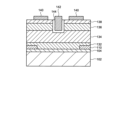
- FIGS. 1A and 1B show a cross-sectional structure of a gallium nitride based semiconductor device 100 according to one embodiment of the present invention.
- a gallium nitride based semiconductor device 100 has a structure in which a conductive alignment layer 104, a gallium nitride based semiconductor layer 106, and an upper electrode layer 108 are arranged on an amorphous substrate 102.
- FIG. Gallium nitride-based semiconductor device 100 further includes an auxiliary electrode layer 110 in contact with conductive alignment layer 104 .
- the conductive orientation layer 104 and the upper electrode layer 108 are used as electrodes, and the gallium nitride based semiconductor layer 106 is used as a functional layer for exhibiting a predetermined function.
- Predetermined functions depend on the structure of the device, but may include functions such as light emission, amplification, switching, and the like.
- a gallium nitride-based semiconductor device refers to a semiconductor device having a gallium nitride layer formed on an amorphous substrate and configured to exhibit a predetermined function.
- Gallium nitride based semiconductor devices may include light emitting devices such as light emitting diodes and active devices such as transistors.
- a gallium nitride-based semiconductor layer refers to a semiconductor layer including at least one gallium nitride layer, and may include a structure in which a plurality of gallium nitride layers having different conductivity types are laminated.
- a glass substrate is used as the amorphous substrate 102 .
- the glass substrate preferably has a low alkali component content, a low thermal expansion coefficient, a high strain point, and a high surface flatness.
- An alkali component is a component that is contained in a large amount in ordinary glass, and the glass substrate used in this embodiment preferably contains an alkali metal such as sodium in an amount of 0.1% or less.
- the glass substrate preferably has an expansion coefficient of less than 50 ⁇ 10 ⁇ 7 /° C. and a strain point of 600° C. or higher. Since the glass substrate does not contain an alkali component and has high heat resistance, a gallium nitride-based semiconductor layer having crystallinity can be formed by a sputtering method to form a semiconductor device, as will be described later.
- the amorphous substrate 102 is not required to have heat resistance of 1000° C. or more like the sapphire substrate. Rather, by using a glass substrate such as that used for liquid crystal displays and organic electroluminescence (organic EL) displays as the amorphous substrate 102, it is possible to fabricate a gallium nitride semiconductor device on a large-area glass substrate called mother glass. can be done. Also, as the amorphous substrate 102, a resin substrate such as a polyimide substrate, an acrylic substrate, a siloxane substrate, or a fluorine resin substrate may be used.
- an insulating layer may be provided on the surface of the amorphous substrate 102 .
- the insulating layer for example, a silicon nitride film, a silicon oxide film, an aluminum oxide film, or the like can be used.
- the insulating layer may be formed by stacking a plurality of types of insulating films, and may have a structure in which, for example, a silicon nitride film and a silicon oxide film are stacked.
- a conductive alignment layer 104 is provided on the amorphous substrate 102 .
- the conductive alignment layer 104 is a crystalline conductive film.
- the crystals of the conductive alignment layer 104 have an orientation, and the crystals are preferably oriented along the c-axis, for example.
- the conductive alignment layer 104 is preferably a crystal with rotational symmetry, for example, the crystal surface preferably has a 6-fold rotational symmetry.
- the conductive alignment layer 104 preferably has a hexagonal close-packed structure, a face-centered cubic structure, or similar structures.
- the structure conforming to the hexagonal close-packed structure or the face-centered cubic structure includes a crystal structure in which the c-axis is not 90 degrees with respect to the a-axis and the b-axis.
- the conductive alignment layer 104 using a conductive material having a hexagonal close-packed structure or similar structure is oriented in the (0001) direction, that is, in the c-axis direction with respect to the amorphous substrate 102 (hereinafter referred to as hexagonal close-packed structure). (0001) orientation of the dense structure is preferred.
- the conductive alignment layer 104 having a face-centered cubic structure or a similar structure is oriented in the (111) direction with respect to the amorphous substrate 102 (hereinafter referred to as the (111) orientation of the face-centered cubic structure). is preferred.
- a conductive alignment layer 104 is provided between the amorphous substrate 102 and the gallium nitride based semiconductor layer 106 .
- the gallium nitride-based semiconductor layer 106 preferably has crystallinity, and the conductive orientation layer 104 functions as a buffer layer. Since the conductive orientation layer 104 has the crystallinity as described above, the gallium nitride based semiconductor layer 106 grown thereon can be crystallized and the crystallization can be promoted.
- the conductive orientation layer 104 has a crystalline surface having six-fold rotational symmetry such as a hexagonal close-packed structure or a face-centered cubic structure, so that the c-axis of the gallium nitride-based semiconductor layer 106 grows in the film thickness direction. can be controlled to
- the crystallinity of the gallium nitride based semiconductor layer 106 is affected by the surface state of the conductive orientation layer 104 . Therefore, the conductive alignment layer 104 preferably has a flat surface. For example, the conductive alignment layer 104 preferably has a surface arithmetic mean roughness (Ra) of less than 2.3 nm. The crystallinity of the gallium nitride based semiconductor layer 106 can be enhanced by the conductive orientation layer 104 having a flat surface.
- the conductive alignment layer 104 is preferably a thin film in order to obtain a flat surface.
- the conductive alignment layer 104 preferably has a thickness of 100 nm or less, preferably 50 nm or less. By setting the film thickness of the conductive alignment layer 104 to 50 nm or less, a flat surface can be formed while maintaining crystallinity.
- the conductive alignment layer 104 preferably has conductivity so that it functions as an electrode of a gallium nitride-based semiconductor device.
- the conductive alignment layer 104 is preferably made of a metal material.
- the conductive alignment layer 104 is preferably made of titanium (Ti), aluminum (Al), and other metals such as silver (Ag), nickel (Ni), copper (Cu), strontium (Sr). , rhodium (Rh), palladium (Pd), iridium (Ir), platinum (Pt), gold (Au), and the like can be used.
- the conductive alignment layer 104 can also be made of conductive metal oxides such as zinc oxide (ZnO) and titanium dioxide (TiO 2 ).
- Such a conductive alignment layer 104 is produced by a sputtering method using a sputtering target made of a metal material for film formation.
- the conductive alignment layer 104 may be fabricated by a vacuum deposition method, an electron beam deposition method.
- the gallium nitride based semiconductor layer 106 includes at least one gallium nitride (GaN) layer.
- Gallium nitride is a compound of gallium (Ga) and nitrogen (N) and is a semiconductor.
- the gallium nitride layer preferably has a stoichiometric composition, but may deviate from the stoichiometric composition.
- the gallium nitride layer used as the gallium nitride based semiconductor layer 106 preferably has crystallinity.
- the crystallinity of the gallium nitride layer is preferably monocrystalline, but may be polycrystalline, microcrystalline, or nanocrystalline.
- the crystal structure of the gallium nitride layer preferably has a wurtzite structure.
- the gallium nitride layer used as the gallium nitride based semiconductor layer 106 preferably has c-axis orientation or (111) orientation.
- the conductivity type of the gallium nitride layer used as the gallium nitride based semiconductor layer 106 may be substantially intrinsic, or may have n-type conductivity or p-type conductivity.
- the gallium nitride layer having n-type conductivity may not contain a dopant for controlling valence electrons, or an element selected from silicon (Si) or germanium (Ge) as an n-type dopant. may be doped.
- the gallium nitride layer having p-type conductivity may be doped with an element selected from magnesium (Mg), zinc (Zn), cadmium (Cd), and beryllium (Be) as a p-type dopant.
- the n-type gallium nitride layer When the n-type gallium nitride layer is added with a dopant, it preferably has a carrier concentration of 1 ⁇ 10 18 /cm 3 or more.
- the p-type gallium nitride layer preferably has a carrier concentration of 5 ⁇ 10 16 /cm 3 or more when a dopant is added.
- the substantially intrinsic (in other words, highly resistive) gallium nitride layer may contain zinc (Zn) as a dopant.
- the gallium nitride layer used as the gallium nitride-based semiconductor layer 106 may contain one or more elements selected from indium (In), aluminum (Al), and arsenic (As). These elements can adjust the bandgap of the gallium nitride layer.
- a gallium nitride layer used as the gallium nitride based semiconductor layer 106 is provided on the conductive alignment layer 104 .
- the surface of the conductive orientation layer 104 (the surface in contact with the gallium nitride layer) contains a crystal plane with rotational symmetry or c-axis orientation, so that gallium nitride having c-axis orientation or (111) orientation layers are obtained.
- the gallium nitride layer may contain an amorphous structure near the interface in contact with the conductive alignment layer 104, but preferably has crystallinity in the bulk.
- the gallium nitride based semiconductor layer 106 having crystallinity can improve the performance of the gallium nitride based semiconductor device 100 . For example, if the gallium nitride-based semiconductor device 100 is a light-emitting device, the emission intensity can be increased, and if it is an active device such as a transistor, the carrier mobility can be increased.
- the gallium nitride based semiconductor layer 106 is deposited at a temperature below the strain point of the amorphous substrate 102 .
- a gallium nitride layer is generally formed by MOCVD (metal-organic chemical vapor deposition), but this film formation method requires a high process temperature, so considering the heat resistance of the amorphous substrate 102, it is not always suitable. I can't say In this embodiment, the gallium nitride-based semiconductor layer 106 is formed by a sputtering method that can be formed at a temperature below the strain point of the amorphous substrate 102 .
- a gallium nitride layer used as the gallium nitride-based semiconductor layer 106 is produced by sputtering while the amorphous substrate 102 is heated to 100 to 600.degree. Since the conductive orientation layer 104 is formed on the deposition surface of the amorphous substrate 102, a gallium nitride layer having crystallinity (preferably c-axis orientation) is formed by a sputtering method even at a substrate temperature of 600° C. or less. can grow.
- the gallium nitride layer used as the gallium nitride-based semiconductor layer 106 is sputtered using a gallium nitride sintered body as a sputtering target and using argon (Ar) or a mixed gas of argon (Ar) and nitrogen (N 2 ) as a sputtering gas. It is made by doing Various methods can be applied to the sputtering.
- a bipolar sputtering method a magnetron sputtering method, a dual magnetron sputtering method, a facing target sputtering method, an ion beam sputtering method, and an inductively coupled plasma (ICP) sputtering method can be applied.
- ICP inductively coupled plasma
- the film thickness of the gallium nitride-based semiconductor layer 106 is not limited, and is appropriately set according to the structure of the device.
- the gallium nitride-based semiconductor layer 106 may be a single layer, or may be a laminate of multiple layers having different conductivity types and/or compositions.
- the upper electrode layer 108 is provided on top of the gallium nitride based semiconductor layer 106 .
- the upper electrode layer 108 functions as an electrode for the gallium nitride based semiconductor device 100 .
- the upper electrode layer 108 is provided to form an ohmic contact with the gallium nitride based semiconductor layer 106 .
- the top electrode layer 108 may be omitted.
- the upper electrode layer 108 is made of a metal material such as aluminum (Al), titanium (Ti), platinum (Pt), nickel (Ni), tantalum (Ta).
- the upper electrode layer 108 may be formed of a metal oxide that has conductivity and is used as a transparent electrode, such as indium tin oxide (ITO), zinc oxide (ZnO), and indium zinc oxide (IZO). .
- the auxiliary electrode layer 110 is provided so as to be in contact with the conductive alignment layer 104 .
- FIG. 1A shows a structure in which an auxiliary electrode layer 110 is provided in contact with the upper surface (the surface facing the gallium nitride-based semiconductor layer 106) and side surfaces of the conductive alignment layer 104.
- FIG. 1B shows a structure in which the auxiliary electrode layer 110 is provided in contact with the lower surface of the conductive alignment layer 104 (the surface facing the amorphous substrate 102). As shown in FIGS. 1A and 1B, the outer peripheral portion of the conductive alignment layer 104 protrudes from the gallium nitride-based semiconductor layer 106, and the protruding portion is in contact with the auxiliary electrode layer 110, thereby increasing the contact area.
- the gallium nitride-based semiconductor layer 106 can be prevented from overlapping the stepped portion formed by the auxiliary electrode layer 110, thereby improving the crystallinity. can be made not to affect
- the auxiliary electrode layer 110 is formed with a thickness of 50 nm or more, preferably 100 nm to 1000 nm, in order to reduce electrical resistance. Therefore, as shown in FIG. 1B, when the auxiliary electrode layer 110 is brought into contact with the lower surface side of the conductive alignment layer 104, it is preferable that the ends have a tapered shape. Since the end of the auxiliary electrode layer 110 has a tapered shape in a cross-sectional view, the conductive alignment layer 104 can be prevented from being disconnected.
- FIGS. 1A and 1B only show a cross-sectional structure
- the auxiliary electrode layer 110 is preferably provided so as to surround the outer circumference of the conductive alignment layer 104 .
- an electrically connected state is formed.
- the conductive alignment layer 104 is used as an electrode of the gallium nitride based semiconductor device 100 .
- the conductive alignment layer 104 has a thickness of 50 nm or less as described above, an increase in electrode resistance becomes a problem.
- the resistivity of titanium (Ti) used as the conductive alignment layer 104 is 100 n ⁇ m, which is one order of magnitude higher than that of aluminum (Al). Therefore, when titanium (Ti) is used as the conductive alignment layer 104, there is concern that the resistance loss of the electrode may adversely affect the device characteristics.
- the gallium nitride-based semiconductor device 100 is a light-emitting device
- a problem may arise in that the light emission intensity becomes non-uniform in the plane. That is, when the conductive alignment layer 104 is connected to a power supply line, a phenomenon can occur in which the emission intensity decreases as the distance from the connection increases.
- the gallium nitride-based semiconductor device 100 shown in FIGS. 1A and 1B is provided with the auxiliary electrode layer 110, thereby solving the problem of the resistance loss of the conductive alignment layer 104.
- the auxiliary electrode layer 110 is electrically connected to the conductive alignment layer 104 and provided to reduce the surface resistivity of the conductive alignment layer 104, thereby eliminating the resistance loss problem. can do.
- the conductive alignment layer 104 can be used as it is as an electrode, and the influence of the high resistance of the electrode can be suppressed. can.
- auxiliary electrode layer 110 As the conductive material forming the auxiliary electrode layer 110 , metal materials such as aluminum (Al), titanium (Ti), silver (Ag), molybdenum (Mo), and tantalum (Ta) are used.
- the auxiliary electrode layer 110 is preferably thicker than the conductive alignment layer 104 for low resistance. Further, the auxiliary electrode layer 110 may have a structure (for example, Ti/Al/Ti) in which an aluminum (Al) film is sandwiched between high melting point metal films such as titanium (Ti) in order to improve heat resistance. good.
- the auxiliary electrode layer 110 is not limited to the structure shown in FIGS. 1A and 1B, and can be provided in various structures. Several embodiments of the auxiliary electrode layer 110 are illustrated below.
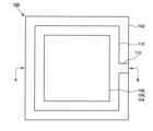
- FIG. 2A and 2B show the structure of a gallium nitride based semiconductor device 100 according to the second embodiment.
- FIG. 2A shows a plan view of a gallium nitride-based semiconductor device 100 according to this embodiment
- FIG. 2B shows a cross-sectional view corresponding to the line AB shown in FIG. 2A.
- the auxiliary electrode layer 110 is in contact with the side and top surfaces of the conductive alignment layer 104 and overlaps the gallium nitride based semiconductor layer 106 on the conductive alignment layer 104. have a structure.
- the auxiliary electrode layer 110 is provided so as to surround the outer periphery of the conductive alignment layer 104 .
- the auxiliary electrode layer 110 may be connected with the wiring 112 .
- the auxiliary electrode layer 110 may be formed of the same conductive layer as the conductive layer forming the wiring 112 . Forming the auxiliary electrode layer 110 and the wiring 112 from the same conductive layer eliminates the need for a connecting portion such as a contact hole, thereby simplifying the structure.
- the provision of the auxiliary electrode layer 110 suppresses deterioration of the characteristics of the gallium nitride-based semiconductor device 100 due to the high resistance of the conductive alignment layer 104. can do.
- the gallium nitride-based semiconductor device 100 is a light-emitting device, uneven brightness in the light-emitting region can be eliminated, and if it is an active device such as a transistor, an increase in power consumption can be suppressed.
- the size of the gallium nitride-based semiconductor device 100 can be reduced because the conductive alignment layer 104 does not need to have protrusions. As a result, the degree of integration can be increased when device integration is attempted.
- the crystallinity of the gallium nitride based semiconductor layer 106 is affected by the conductive orientation layer 104 . Since the auxiliary electrode layer 110 is a thick film and has a crystallinity different from that of the conductive orientation layer 104, there is concern that the gallium nitride based semiconductor layer 106 will be affected. Specifically, the crystallinity of the outer peripheral portion 114 of the gallium nitride based semiconductor layer 106 shown in FIGS. 2A and 2B may differ from the crystallinity of the region inside the outer peripheral portion 114 of the gallium nitride based semiconductor layer 106 .
- the outer peripheral portion 114 of the gallium nitride-based semiconductor layer 106 may be affected by the auxiliary electrode layer 110 and may be in an amorphous state with poorer crystallinity than the inner region. In this case, if the resistance of the outer peripheral portion 114 is increased, the leakage current flowing through the end surface of the gallium nitride based semiconductor layer 106 between the upper electrode layer 108 and the auxiliary electrode layer 110 can be reduced.
- the width over which the auxiliary electrode layer 110 overlaps the gallium nitride based semiconductor layer 106 is slightly smaller than the full width of the gallium nitride based semiconductor layer 106 . Therefore, as described above, even if a region with different crystallinity is formed in the outer peripheral portion 114, the effect on the gallium nitride based semiconductor device 100 is slight. Rather, by providing the gallium nitride-based semiconductor device 100 with the auxiliary electrode layer 110, it is possible to obtain the advantage of eliminating the influence of the conductive orientation layer 104 having a high resistance.
- the gallium nitride-based semiconductor device 100 is the same as that shown in the first embodiment, except that the auxiliary electrode layer 110 has a region overlapping the gallium nitride-based semiconductor layer 106, and obtains the same effects. be able to.
- FIG. 3A and 3B show the structure of a gallium nitride based semiconductor device 100 according to the third embodiment.
- FIG. 3A shows a plan view of a gallium nitride-based semiconductor device 100 according to this embodiment
- FIG. 3B shows a cross-sectional view corresponding to AB shown in FIG. 3A.
- the gallium nitride based semiconductor device 100 shown in FIGS. 3A and 3B has a structure in which the auxiliary electrode layer 110 is in contact with the lower surface of the conductive alignment layer 104 .
- the auxiliary electrode layer 110 is provided so as to surround the outer periphery of the conductive alignment layer 104 .
- the auxiliary electrode layer 110 may be connected to the wiring 112 , and the auxiliary electrode layer 110 may be formed of the same conductive layer as the conductive layer forming the wiring 112 .
- the structure in which the auxiliary electrode layer 110 is in contact with the lower surface of the conductive alignment layer 104 causes the gallium nitride-based semiconductor layer 106 to have a structure in which the entire lower surface thereof is in contact with the conductive alignment layer 104 . Therefore, the crystallinity of the gallium nitride based semiconductor layer 106 becomes uniform over the entire surface.
- the gallium nitride-based semiconductor layer 106 includes a portion that overlaps a step formed by the conductive alignment layer 104 overlapping the auxiliary electrode layer 110 . However, as in the second embodiment, the area of the stepped portion occupies a small proportion of the total area, and the effect on the gallium nitride based semiconductor device 100 is minor.
- the structure shown in FIGS. 3A and 3B can be said to be a structure in which the gallium nitride based semiconductor layer 106 is less susceptible to the formation of the auxiliary electrode layer than the structure shown in the first embodiment.
- the gallium nitride-based semiconductor device 100 according to this embodiment is the same as that shown in the second embodiment, except that the auxiliary electrode layer 110 is in contact with the lower surface of the conductive alignment layer 104, and the same effects can be obtained. can be done.
- FIG. 4A and 4B show the structure of a gallium nitride based semiconductor device 100 according to the fourth embodiment.
- 4A shows a plan view of a gallium nitride-based semiconductor device 100 according to this embodiment
- FIG. 4B shows a cross-sectional view corresponding to the line AB shown in FIG. 4A.
- the gallium nitride-based semiconductor device 100 shown in FIGS. 4A and 4B has a structure in which the auxiliary electrode layer 110 is in contact with the side surface of the conductive alignment layer 104 .
- the auxiliary electrode layer 110 may be in contact with the side surfaces of the gallium nitride based semiconductor layer 106 as well as the conductive alignment layer 104 .
- the auxiliary electrode layer 110 is preferably provided so as to be in contact with the outer peripheral side surfaces of the conductive alignment layer 104 and the gallium nitride based semiconductor layer 106 over the entire circumference.
- the gallium nitride-based semiconductor layer 106 may have a multilayer structure.
- the gallium nitride based semiconductor device 100 is a light emitting device
- the gallium nitride based semiconductor layer 106 is formed by laminating an n-type gallium nitride semiconductor layer, an active layer (light emitting layer), and a p-type gallium nitride semiconductor layer from the lower layer side. structure.
- the auxiliary electrode layer 110 is preferably provided so as to be in contact with the side surface of the n-type gallium nitride semiconductor layer, which is the bottom layer.
- the auxiliary electrode layer 110 shown in FIGS. 4A and 4B is formed after forming the gallium nitride based semiconductor layer 106 and the upper electrode layer 108 on the conductive alignment layer 104 . Specifically, after a laminate of a conductive alignment layer 104, a gallium nitride-based semiconductor layer 106, and an upper electrode layer 108 is formed on the amorphous substrate 102 as shown in FIG. A conductive film is formed to cover the top surface and side surfaces of the stack. Then, the auxiliary electrode layer 110 can be formed by etching back the conductive film by anisotropic etching so that the conductive layer remains on the side surface of the laminate.
- a conductive film for forming the auxiliary electrode layer 110 is made of a metal material such as titanium (Ti), aluminum (Al), silver (Ag), molybdenum (Mo), or tantalum (Ta).
- the auxiliary electrode layer 110 may be connected with traces 112 to connect with adjacent devices or power sources.
- the auxiliary electrode layer 110 By providing the auxiliary electrode layer 110 so as to be in contact with the side surface of the conductive alignment layer 104 in this way, it is possible to prevent the formation of the gallium nitride based semiconductor layer 106 from being affected.
- the gallium nitride based semiconductor layer 106 is formed on the conductive orientation layer 104, the upper electrode layer 108 is formed, and then the auxiliary electrode layer 110 is formed. It can be made not to affect the crystallinity. This makes it possible to obtain good device characteristics.
- the gallium nitride-based semiconductor device 100 according to this embodiment is the same as that shown in the first embodiment, except that the auxiliary electrode layer 110 is in contact with the side surface of the conductive alignment layer 104, and has the same effects. can be obtained.
- FIG. 5A and 5B show the structure of a gallium nitride based semiconductor device 100 according to the third embodiment.
- FIG. 5A shows a plan view of a gallium nitride-based semiconductor device 100 according to this embodiment
- FIG. 5B shows a cross-sectional view corresponding to AB shown in FIG. 5A.
- the gallium nitride-based semiconductor device 100 shown in FIGS. 5A and 5B has a structure in which the auxiliary electrode layer 110 is in contact with the entire bottom surface of the conductive alignment layer 104 .
- the auxiliary electrode layer 110 may have a structure continuous from the wiring 112 , and the auxiliary electrode layer 110 may be formed of the same conductive layer as the conductive layer forming the wiring 112 .
- the auxiliary electrode layer 110 may have a larger area than the conductive alignment layer 104 and may be edged outward.
- the auxiliary electrode layer 110 may have the same size as the conductive alignment layer 104 or a smaller area than the conductive alignment layer 104, and the ends thereof may be lined inside.
- the contact area can be increased, and the resistance can be more effectively reduced. . That is, the sheet resistance (surface resistance) of the conductive alignment layer 104 can be substantially reduced.
- the structure shown in FIGS. 5A and 5B has a structure in which the gallium nitride-based semiconductor layer 106 is in contact with the entire surface of the conductive orientation layer 104 . Therefore, the crystallinity of the gallium nitride based semiconductor layer 106 can be made uniform. In addition, if the area of the auxiliary electrode layer 110 is increased, the conductive alignment layer 104 does not have a stepped portion, so that the influence of the stepped portion can be eliminated. As described above, the structures shown in FIGS. 5A and 5B have structures in which the gallium nitride-based semiconductor layer 106 is less susceptible to the formation of the auxiliary electrode layer than the structures shown in the second and third embodiments. .
- the gallium nitride-based semiconductor device 100 according to this embodiment is the same as that shown in the first embodiment, except that the auxiliary electrode layer 110 is in contact with the lower surface of the conductive alignment layer 104, and the same effects can be obtained. can be done.
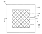
- FIG. 6A and 6B show the structure of a gallium nitride based semiconductor device 100 according to the sixth embodiment.
- FIG. 6A shows a plan view of a gallium nitride-based semiconductor device 100 according to this embodiment
- FIG. 6B shows a cross-sectional view corresponding to AB shown in FIG. 6A.
- the gallium nitride-based semiconductor device 100 shown in FIGS. 6A and 6B has a structure in which the auxiliary electrode layer 110 has a grid-like pattern and is provided on the upper surface of the conductive alignment layer 104 .
- the grid-like pattern of the auxiliary electrode layer 110 is provided to extend over the entire surface of the conductive alignment layer 104 .
- the auxiliary electrode layer 110 having a lattice pattern may be connected to the wiring 112 at the end.
- the auxiliary electrode layer 110 is formed of a metal material such as aluminum (Al), silver (Ag), etc., which has a lower resistance than the metal forming the conductive alignment layer 104 .
- the line width of the lattice pattern is narrowed so as to minimize the influence on the crystallinity of the gallium nitride based semiconductor layer 106 .
- the structure of the auxiliary electrode layer 110 shown in FIGS. 6A and 6B can substantially reduce the sheet resistance (surface resistance) of the conductive alignment layer 104.
- the lattice pattern of the auxiliary electrode layer 110 spreads over the entire surface of the conductive alignment layer 104, which is advantageous for increasing the area. For example, when the gallium nitride-based semiconductor device 100 is a light-emitting device, luminance unevenness (luminance gradient) can be suppressed even if the light-emitting region is enlarged.
- a gallium nitride-based semiconductor device 100 shown in FIGS. 7A and 7B has a structure in which an auxiliary electrode layer 110 having a grid-like pattern is provided so as to be in contact with the lower surface of a conductive alignment layer 104 .
- FIG. 7A shows a plan view of the gallium nitride-based semiconductor device 100 according to this embodiment
- FIG. 7B shows a cross-sectional view corresponding to AB shown in FIG. 7A.
- the auxiliary electrode layer 110 having a lattice pattern is provided between the amorphous substrate 102 and the conductive alignment layer 104 so that the entire surface of the gallium nitride based semiconductor layer 106 is in contact with the conductive alignment layer 104. and good crystallinity can be obtained.
- the lattice pattern of the auxiliary electrode layer 110 may be replaced with a stripe pattern or a mesh pattern.
- the configuration of the auxiliary electrode layer 110 shown in this embodiment can be appropriately combined with the auxiliary electrode layers shown in the first to fourth embodiments.
- the grid pattern shown in this embodiment is connected to the auxiliary electrode layer 110 arranged on the outer periphery of the conductive alignment layer 104 shown in the first embodiment, and the outer periphery of the conductive alignment layer 104 is connected.
- a configuration in which the auxiliary electrode layer 110 is provided in the portion and in the plane may be adopted.
- the gallium nitride-based semiconductor device 100 according to this embodiment is the same as that shown in the first embodiment, except that the auxiliary electrode layer 110 is in contact with the lower surface of the conductive alignment layer 104, and the same effects can be obtained. can be done.
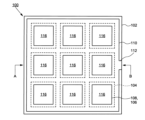
- FIG. 8A and 8B show the structure of a gallium nitride based semiconductor device 100 according to the seventh embodiment.
- 8A shows a plan view of a gallium nitride-based semiconductor device 100 according to this embodiment
- FIG. 8B shows a cross-sectional view corresponding to the line AB shown in FIG. 8A.
- FIG. 8A and 8B show a gallium nitride based semiconductor device 100 in which a plurality of stacked stacks 116 of conductive alignment layers 104, gallium nitride based semiconductor layers 106, and top electrode layers 108 are disposed on an amorphous substrate 102.
- Each laminate 116 has the structure shown in the second embodiment.
- a plurality of laminates 116 are spaced apart on the amorphous substrate 102, and an auxiliary electrode layer 110 is provided in a region where the plurality of laminates 116 are spaced apart.
- the auxiliary electrode layer 110 is provided to connect adjacent laminates 116 .
- the auxiliary electrode layer 110 is arranged so as to spread over the entire region where the multiple laminates 116 are arranged. With such an arrangement, it is possible not only to electrically connect the plurality of stacked bodies 116 but also to reduce the resistance.
- FIGS. 9A and 9B show the case where each of the plurality of laminates 116 has the same structure as the structure shown in the third embodiment.
- FIG. 9A shows a plan view of the gallium nitride-based semiconductor device 100
- FIG. 9B shows a cross-sectional view corresponding to the line AB shown in FIG. 9A.
- the configuration in which the auxiliary electrode layer 110 is arranged on the lower layer side of the conductive alignment layer 104 can also connect adjacent stacks 116 .
- FIGS. 8A and 8B and 9A and 9B show an example in which all of the conductive alignment layers 104 of the multiple laminates 116 are connected to the same potential, but the configuration of the auxiliary electrode layer 110 is shown. is not limited to the examples.
- a structure in which the auxiliary electrode layer 110 is provided so that the plurality of laminates 116 arranged in a matrix are connected in the row direction or the column direction, and the plurality of laminates 116 are connected in series and parallel on the amorphous substrate 102. may be formed.
- the gallium nitride-based semiconductor device 100 shown in this embodiment is advantageous, for example, in realizing a relatively large-area light-emitting device.
- the plurality of laminates 116 do not need to increase the area of each, can prevent luminance unevenness due to the resistance of the conductive alignment layer 104, and can achieve low resistance by the auxiliary electrode layer 110.
- FIG. As a result, it is possible to obtain a light-emitting device having a uniform luminance distribution during light emission.
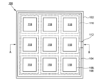
- FIG. 10A and 10B show the structure of a gallium nitride based semiconductor device 100 according to the eighth embodiment.
- FIG. 10A shows a plan view of a gallium nitride-based semiconductor device 100 according to this embodiment
- FIG. 10B shows a cross-sectional view corresponding to AB shown in FIG. 10A.
- a gallium nitride-based semiconductor device 100 shown in FIGS. 10A and 10B has a configuration in which a plurality of laminated bodies 118 are provided as in the seventh embodiment, but the structure of the conductive orientation layer 104 is different.
- the conductive alignment layer 104 is continuous and has a structure commonly provided over a plurality of laminates 118 .
- the gallium nitride-based semiconductor device 100 according to the present embodiment has a conductive orientation layer 104 provided on an amorphous substrate 102, and a plurality of divided gallium nitride-based semiconductor layers and upper electrodes are formed thereon. is arranged.
- the auxiliary electrode layer 110 is provided so as to be in contact with the upper surface of the conductive alignment layer 104 in a region where the gallium nitride-based semiconductor layer 106 divided into a plurality of parts is separated.
- the auxiliary electrode layer 110 is provided on the conductive alignment layer 104 in a lattice pattern, and the gallium nitride based semiconductor layer 106 and the upper electrode layer 108 are formed in the openings of the lattice. pattern is placed.
- the thickness of the auxiliary electrode layer 110 can be increased, and the resistance of the auxiliary electrode of the conductive alignment layer 104 can be reduced.
- FIGS. 11A and 11B show a structure in which the auxiliary electrode layer 110 is provided on the lower layer side of the conductive alignment layer 104.
- FIG. 11A shows a plan view of the gallium nitride-based semiconductor device 100
- FIG. 11B shows a cross-sectional view corresponding to AB shown in FIG. 11A.
- a configuration in which the auxiliary electrode layer 110 is arranged on the lower layer side of the conductive alignment layer 104 can also achieve low resistance.
- the gallium nitride-based semiconductor device 100 shown in this embodiment is advantageous in realizing a relatively large-area light-emitting device, as in the seventh embodiment. It is not necessary to increase the area of each light emitting region, and the provision of the auxiliary electrode layer 110 can prevent luminance unevenness caused by the resistance of the conductive alignment layer 104 . This makes it possible to obtain a light-emitting device with a uniform luminance distribution during light emission.
- FIG. 12A shows the configuration of the gallium nitride based semiconductor layer 106 when the gallium nitride based semiconductor device 100 is a light emitting device.
- the gallium nitride based semiconductor layer 106 has a structure in which an n-type gallium nitride layer 120 , a light emitting layer 124 and a p-type gallium nitride layer 130 are laminated on the conductive alignment layer 104 .
- An upper electrode layer 108 is provided on the p-type gallium nitride layer 130 .
- the upper electrode layer 108 is made of a metal material such as gold (Au), a titanium (Ti)-gold (Au) alloy, or a transparent conductive film such as indium tin oxide (ITO).
- the structure of the light emitting layer 124 may vary, and may be formed by quantum well layers in which gallium nitride (GaN) layers and indium gallium nitride (InGaN) layers are alternately stacked.
- FIG. 12B shows another configuration of the gallium nitride based semiconductor layer 106 included in the light emitting device.
- 12B has a structure in which an n-type gallium nitride layer 120, an n-type aluminum gallium nitride layer 122, an indium gallium nitride layer 126, a p-type aluminum gallium nitride layer 128, and a p-type gallium nitride layer 130 are laminated.
- Each of these layers is produced by a sputtering method. Since each layer has a different composition, it is formed using a sputtering target containing a dopant corresponding to each conductivity type.
- n-type dopant an element selected from silicon (Si) and germanium (Ge) can be used, and as a p-type dopant, magnesium (Mg), zinc (Zn), and cadmium (Cd) can be used. , and beryllium (Be). Since these layers are preferably formed continuously in vacuum, a multi-chamber sputtering apparatus is used.
- FIG. 13 shows the configuration of the gallium nitride based semiconductor layer 106 when the gallium nitride based semiconductor device 100 is a transistor.
- the gallium nitride-based semiconductor layer 106 has a structure in which an n + -type gallium nitride layer 132, an n-type gallium nitride layer 134, a p-type gallium nitride layer 136, and an n-type gallium nitride layer 138 are laminated on the conductive orientation layer 104.
- a source electrode 140 is provided on the n-type gallium nitride layer 138 and the conductive alignment layer 104 is used as the drain electrode.
- the gate electrode 142 has a trench gate structure and is provided so as to be embedded in the p-type gallium nitride layer 130 via the gate insulating layer 144 .
- Each layer of the gallium nitride based semiconductor layer 106 is produced by a sputtering method.
- the configuration of the gallium nitride based semiconductor layer 106 shown in this embodiment can be applied to the configurations shown in the first to eighth embodiments. As shown in FIGS. 12A, 12B, and 13, the gallium nitride-based semiconductor layer 106 can have various laminated structures, and devices can be configured according to applications.
- FIG. 14 is a schematic diagram showing the configuration of a light emitting device 150 according to an embodiment of the invention.
- a light-emitting device 150 has a pixel portion 152 and a terminal portion 154 formed on an amorphous substrate 102 .
- the pixel portion 152 is formed in the central portion of the amorphous substrate 102 and the terminal portion 154 is formed in the edge portion of the amorphous substrate 102 .
- the pixel portion 152 includes a plurality of pixels 156 arranged in a matrix. Each of the plurality of pixels 156 is provided with a light-emitting device having the structure shown in the first to sixth embodiments.
- Terminal portion 154 includes a plurality of terminals 158 .
- a power supply line is connected to each of the plurality of terminals 158 so that voltage can be applied (current can be supplied) to the light emitting device in the pixel 156 .
- a transistor may be provided in the pixel 156 and light emission of the light emitting device may be controlled by the transistor.
- 100 gallium nitride based semiconductor device, 102: amorphous substrate, 104: conductive orientation layer, 106: gallium nitride based semiconductor layer, 108: upper electrode layer, 110: auxiliary electrode layer, 112: wiring, 114: peripheral portion, 116 : laminated body 118: laminated body 120: n-type gallium nitride layer 122: n-type aluminum gallium nitride layer 124: light emitting layer 126: indium gallium nitride layer 128: p-type aluminum gallium nitride layer 130: p type gallium nitride layer, 132: n + type gallium nitride layer, 134: n type gallium nitride layer, 136: p type gallium nitride layer, 138: n type gallium nitride layer, 140: source electrode, 142: gate electrode, 144: Gate insulating layer 150: light emitting device 152: pixel
Landscapes
- Engineering & Computer Science (AREA)
- Microelectronics & Electronic Packaging (AREA)
- Power Engineering (AREA)
- Computer Hardware Design (AREA)
- Manufacturing & Machinery (AREA)
- Physics & Mathematics (AREA)
- Condensed Matter Physics & Semiconductors (AREA)
- General Physics & Mathematics (AREA)
- Ceramic Engineering (AREA)
- Led Devices (AREA)
Abstract
L'invention concerne un dispositif à semi-conducteurs à base de nitrure de gallium comprenant un substrat amorphe, une couche d'alignement conductrice sur le substrat amorphe, une couche semi-conductrice à base de nitrure de gallium sur la couche d'alignement conductrice, et une couche d'électrode auxiliaire en contact avec la couche d'alignement conductrice. La couche d'alignement conductrice est de préférence un film métallique orienté sur l'axe c ou un film d'oxyde métallique, et la couche d'électrode auxiliaire est disposée de manière à entourer la périphérie extérieure de la couche d'alignement conductrice.
Priority Applications (2)
| Application Number | Priority Date | Filing Date | Title |
|---|---|---|---|
| CN202280057169.3A CN117836959A (zh) | 2021-09-03 | 2022-08-04 | 无定形基板上的氮化镓系半导体器件 |
| JP2023545181A JPWO2023032583A1 (fr) | 2021-09-03 | 2022-08-04 |
Applications Claiming Priority (2)
| Application Number | Priority Date | Filing Date | Title |
|---|---|---|---|
| JP2021-144296 | 2021-09-03 | ||
| JP2021144296 | 2021-09-03 |
Publications (1)
| Publication Number | Publication Date |
|---|---|
| WO2023032583A1 true WO2023032583A1 (fr) | 2023-03-09 |
Family
ID=85410974
Family Applications (1)
| Application Number | Title | Priority Date | Filing Date |
|---|---|---|---|
| PCT/JP2022/029875 WO2023032583A1 (fr) | 2021-09-03 | 2022-08-04 | Dispositif à semi-conducteurs à base de nitrure de gallium sur substrat amorphe |
Country Status (3)
| Country | Link |
|---|---|
| JP (1) | JPWO2023032583A1 (fr) |
| CN (1) | CN117836959A (fr) |
| WO (1) | WO2023032583A1 (fr) |
Citations (5)
| Publication number | Priority date | Publication date | Assignee | Title |
|---|---|---|---|---|
| JPS5710280A (en) * | 1980-06-23 | 1982-01-19 | Futaba Corp | Gan light emitting element |
| JPH08139361A (ja) * | 1994-11-08 | 1996-05-31 | Toshiba Corp | 化合物半導体発光素子 |
| JPH0936427A (ja) * | 1995-07-18 | 1997-02-07 | Showa Denko Kk | 半導体装置及びその製造方法 |
| US20020125821A1 (en) * | 2001-03-12 | 2002-09-12 | University Of Cincinnati | Electroluminescent display formed on glass with a thick film dielectric layer |
| JP2006310527A (ja) * | 2005-04-28 | 2006-11-09 | Institute Of National Colleges Of Technology Japan | アモルファス材料基板を用いた発光素子及びその製造方法 |
-
2022
- 2022-08-04 JP JP2023545181A patent/JPWO2023032583A1/ja active Pending
- 2022-08-04 CN CN202280057169.3A patent/CN117836959A/zh active Pending
- 2022-08-04 WO PCT/JP2022/029875 patent/WO2023032583A1/fr active Application Filing
Patent Citations (5)
| Publication number | Priority date | Publication date | Assignee | Title |
|---|---|---|---|---|
| JPS5710280A (en) * | 1980-06-23 | 1982-01-19 | Futaba Corp | Gan light emitting element |
| JPH08139361A (ja) * | 1994-11-08 | 1996-05-31 | Toshiba Corp | 化合物半導体発光素子 |
| JPH0936427A (ja) * | 1995-07-18 | 1997-02-07 | Showa Denko Kk | 半導体装置及びその製造方法 |
| US20020125821A1 (en) * | 2001-03-12 | 2002-09-12 | University Of Cincinnati | Electroluminescent display formed on glass with a thick film dielectric layer |
| JP2006310527A (ja) * | 2005-04-28 | 2006-11-09 | Institute Of National Colleges Of Technology Japan | アモルファス材料基板を用いた発光素子及びその製造方法 |
Also Published As
| Publication number | Publication date |
|---|---|
| JPWO2023032583A1 (fr) | 2023-03-09 |
| CN117836959A (zh) | 2024-04-05 |
Similar Documents
| Publication | Publication Date | Title |
|---|---|---|
| TWI436494B (zh) | Nitride semiconductor components | |
| JP5385614B2 (ja) | 光学素子およびその製造方法 | |
| KR102625489B1 (ko) | 마이크로 led 표시 패널 및 그 제조 방법 | |
| CN101960625B (zh) | 半导体发光元件、该半导体发光元件的制造方法以及使用该半导体发光元件的灯 | |
| CN100541843C (zh) | 一种氮化镓基发光二极管p型层透明导电膜及其制作方法 | |
| US8436396B2 (en) | Semiconductor light emitting element, method for manufacturing semiconductor light emitting element, and lamp | |
| WO2010021106A1 (fr) | Dispositif à semi-conducteurs, procédé de fabrication de dispositif à semi-conducteurs, substrat de transistor, dispositif d'émission de lumière et dispositif d'affichage | |
| CN101944537B (zh) | 有机发光二极管显示装置及其制造方法 | |
| CN102017200B (zh) | 发光器件和制造发光器件的方法 | |
| TWI729612B (zh) | 主動矩陣led陣列前驅物 | |
| KR20100103866A (ko) | 고성능 헤테로구조 발광 소자 및 방법 | |
| CN108987480A (zh) | 双栅薄膜晶体管及其制备方法、显示面板及其制备方法 | |
| US7981710B2 (en) | Light emitting device and manufacturing method | |
| CN109216395B (zh) | 发光结构、发光晶体管及其制造方法 | |
| US8304979B2 (en) | Light emitting device having inorganic luminescent particles in inorganic hole transport material | |
| WO2023032583A1 (fr) | Dispositif à semi-conducteurs à base de nitrure de gallium sur substrat amorphe | |
| WO2010035369A1 (fr) | Élément électroluminescent et dispositif d'affichage | |
| JP2009152530A (ja) | 窒化物半導体発光素子及びその製造方法 | |
| WO2023248753A1 (fr) | Dispositif semi-conducteur à base de nitrure de gallium sur un substrat amorphe et son procédé de fabrication | |
| WO2023074098A1 (fr) | Dispositif d'affichage et son procédé de production | |
| WO2024116849A1 (fr) | Élément redresseur | |
| WO2023058308A1 (fr) | Dispositif électroluminescent et substrat de formation de dispositif électroluminescent | |
| WO2024048004A1 (fr) | Structure stratifiée, dispositif à semi-conducteur et leur procédé de fabrication | |
| JP5100180B2 (ja) | 発光素子および製造方法 | |
| WO2024048394A1 (fr) | Structure stratifiée, procédé de fabrication de structure stratifiée et dispositif à semi-conducteur |
Legal Events
| Date | Code | Title | Description |
|---|---|---|---|
| 121 | Ep: the epo has been informed by wipo that ep was designated in this application |
Ref document number: 22864169 Country of ref document: EP Kind code of ref document: A1 |
|
| WWE | Wipo information: entry into national phase |
Ref document number: 2023545181 Country of ref document: JP |
|
| WWE | Wipo information: entry into national phase |
Ref document number: 202280057169.3 Country of ref document: CN |
|
| NENP | Non-entry into the national phase |
Ref country code: DE |