WO2023032583A1 - Gallium nitride-based semiconductor device on amorphous substrate - Google Patents
Gallium nitride-based semiconductor device on amorphous substrate Download PDFInfo
- Publication number
- WO2023032583A1 WO2023032583A1 PCT/JP2022/029875 JP2022029875W WO2023032583A1 WO 2023032583 A1 WO2023032583 A1 WO 2023032583A1 JP 2022029875 W JP2022029875 W JP 2022029875W WO 2023032583 A1 WO2023032583 A1 WO 2023032583A1
- Authority
- WO
- WIPO (PCT)
- Prior art keywords
- gallium nitride
- layer
- based semiconductor
- semiconductor device
- auxiliary electrode
- Prior art date
Links
- 229910002601 GaN Inorganic materials 0.000 title claims abstract description 250
- JMASRVWKEDWRBT-UHFFFAOYSA-N Gallium nitride Chemical compound [Ga]#N JMASRVWKEDWRBT-UHFFFAOYSA-N 0.000 title claims abstract description 248
- 239000004065 semiconductor Substances 0.000 title claims abstract description 178
- 239000000758 substrate Substances 0.000 title claims abstract description 60
- 229910052751 metal Inorganic materials 0.000 claims abstract description 9
- 239000002184 metal Substances 0.000 claims abstract description 9
- 229910044991 metal oxide Inorganic materials 0.000 claims abstract description 5
- 150000004706 metal oxides Chemical class 0.000 claims abstract description 5
- 239000010936 titanium Substances 0.000 claims description 20
- 239000011521 glass Substances 0.000 claims description 11
- 230000002093 peripheral effect Effects 0.000 claims description 11
- PXHVJJICTQNCMI-UHFFFAOYSA-N Nickel Chemical compound [Ni] PXHVJJICTQNCMI-UHFFFAOYSA-N 0.000 claims description 9
- RTAQQCXQSZGOHL-UHFFFAOYSA-N Titanium Chemical group [Ti] RTAQQCXQSZGOHL-UHFFFAOYSA-N 0.000 claims description 9
- 229910052782 aluminium Inorganic materials 0.000 claims description 9
- XAGFODPZIPBFFR-UHFFFAOYSA-N aluminium Chemical compound [Al] XAGFODPZIPBFFR-UHFFFAOYSA-N 0.000 claims description 9
- BASFCYQUMIYNBI-UHFFFAOYSA-N platinum Chemical compound [Pt] BASFCYQUMIYNBI-UHFFFAOYSA-N 0.000 claims description 9
- 229910052719 titanium Inorganic materials 0.000 claims description 9
- 239000010931 gold Substances 0.000 claims description 8
- KDLHZDBZIXYQEI-UHFFFAOYSA-N Palladium Chemical compound [Pd] KDLHZDBZIXYQEI-UHFFFAOYSA-N 0.000 claims description 6
- BQCADISMDOOEFD-UHFFFAOYSA-N Silver Chemical compound [Ag] BQCADISMDOOEFD-UHFFFAOYSA-N 0.000 claims description 5
- 229910052709 silver Inorganic materials 0.000 claims description 5
- 239000004332 silver Substances 0.000 claims description 5
- 239000010949 copper Substances 0.000 claims description 4
- 229910052737 gold Inorganic materials 0.000 claims description 4
- 239000010948 rhodium Substances 0.000 claims description 4
- XLOMVQKBTHCTTD-UHFFFAOYSA-N Zinc monoxide Chemical compound [Zn]=O XLOMVQKBTHCTTD-UHFFFAOYSA-N 0.000 claims description 3
- PCHJSUWPFVWCPO-UHFFFAOYSA-N gold Chemical compound [Au] PCHJSUWPFVWCPO-UHFFFAOYSA-N 0.000 claims description 3
- 229910052759 nickel Inorganic materials 0.000 claims description 3
- 229910052697 platinum Inorganic materials 0.000 claims description 3
- RYGMFSIKBFXOCR-UHFFFAOYSA-N Copper Chemical compound [Cu] RYGMFSIKBFXOCR-UHFFFAOYSA-N 0.000 claims description 2
- GWEVSGVZZGPLCZ-UHFFFAOYSA-N Titan oxide Chemical compound O=[Ti]=O GWEVSGVZZGPLCZ-UHFFFAOYSA-N 0.000 claims description 2
- 229910052802 copper Inorganic materials 0.000 claims description 2
- 229910052741 iridium Inorganic materials 0.000 claims description 2
- GKOZUEZYRPOHIO-UHFFFAOYSA-N iridium atom Chemical compound [Ir] GKOZUEZYRPOHIO-UHFFFAOYSA-N 0.000 claims description 2
- 229910052763 palladium Inorganic materials 0.000 claims description 2
- 229910052703 rhodium Inorganic materials 0.000 claims description 2
- MHOVAHRLVXNVSD-UHFFFAOYSA-N rhodium atom Chemical compound [Rh] MHOVAHRLVXNVSD-UHFFFAOYSA-N 0.000 claims description 2
- 229910052712 strontium Inorganic materials 0.000 claims description 2
- CIOAGBVUUVVLOB-UHFFFAOYSA-N strontium atom Chemical compound [Sr] CIOAGBVUUVVLOB-UHFFFAOYSA-N 0.000 claims description 2
- 239000010410 layer Substances 0.000 description 398
- 239000010408 film Substances 0.000 description 19
- 238000004544 sputter deposition Methods 0.000 description 14
- 238000000034 method Methods 0.000 description 10
- 239000002019 doping agent Substances 0.000 description 9
- 230000000694 effects Effects 0.000 description 9
- 239000013078 crystal Substances 0.000 description 7
- 239000007769 metal material Substances 0.000 description 7
- 150000001875 compounds Chemical class 0.000 description 6
- 230000015572 biosynthetic process Effects 0.000 description 5
- XKRFYHLGVUSROY-UHFFFAOYSA-N Argon Chemical compound [Ar] XKRFYHLGVUSROY-UHFFFAOYSA-N 0.000 description 4
- RNQKDQAVIXDKAG-UHFFFAOYSA-N aluminum gallium Chemical compound [Al].[Ga] RNQKDQAVIXDKAG-UHFFFAOYSA-N 0.000 description 4
- 229910052738 indium Inorganic materials 0.000 description 4
- APFVFJFRJDLVQX-UHFFFAOYSA-N indium atom Chemical compound [In] APFVFJFRJDLVQX-UHFFFAOYSA-N 0.000 description 4
- 239000011777 magnesium Substances 0.000 description 4
- 239000000203 mixture Substances 0.000 description 4
- 229910052594 sapphire Inorganic materials 0.000 description 4
- 239000010980 sapphire Substances 0.000 description 4
- IJGRMHOSHXDMSA-UHFFFAOYSA-N Atomic nitrogen Chemical compound N#N IJGRMHOSHXDMSA-UHFFFAOYSA-N 0.000 description 3
- 239000003513 alkali Substances 0.000 description 3
- 238000005477 sputtering target Methods 0.000 description 3
- 229910052715 tantalum Inorganic materials 0.000 description 3
- GUVRBAGPIYLISA-UHFFFAOYSA-N tantalum atom Chemical compound [Ta] GUVRBAGPIYLISA-UHFFFAOYSA-N 0.000 description 3
- JBQYATWDVHIOAR-UHFFFAOYSA-N tellanylidenegermanium Chemical compound [Te]=[Ge] JBQYATWDVHIOAR-UHFFFAOYSA-N 0.000 description 3
- FYYHWMGAXLPEAU-UHFFFAOYSA-N Magnesium Chemical compound [Mg] FYYHWMGAXLPEAU-UHFFFAOYSA-N 0.000 description 2
- ZOKXTWBITQBERF-UHFFFAOYSA-N Molybdenum Chemical compound [Mo] ZOKXTWBITQBERF-UHFFFAOYSA-N 0.000 description 2
- 229910052581 Si3N4 Inorganic materials 0.000 description 2
- VYPSYNLAJGMNEJ-UHFFFAOYSA-N Silicium dioxide Chemical compound O=[Si]=O VYPSYNLAJGMNEJ-UHFFFAOYSA-N 0.000 description 2
- XUIMIQQOPSSXEZ-UHFFFAOYSA-N Silicon Chemical compound [Si] XUIMIQQOPSSXEZ-UHFFFAOYSA-N 0.000 description 2
- 229910052786 argon Inorganic materials 0.000 description 2
- 229910052790 beryllium Inorganic materials 0.000 description 2
- ATBAMAFKBVZNFJ-UHFFFAOYSA-N beryllium atom Chemical compound [Be] ATBAMAFKBVZNFJ-UHFFFAOYSA-N 0.000 description 2
- 229910052793 cadmium Inorganic materials 0.000 description 2
- BDOSMKKIYDKNTQ-UHFFFAOYSA-N cadmium atom Chemical compound [Cd] BDOSMKKIYDKNTQ-UHFFFAOYSA-N 0.000 description 2
- 230000008859 change Effects 0.000 description 2
- 238000005229 chemical vapour deposition Methods 0.000 description 2
- 239000004020 conductor Substances 0.000 description 2
- 230000007423 decrease Effects 0.000 description 2
- 238000009826 distribution Methods 0.000 description 2
- 238000005530 etching Methods 0.000 description 2
- 239000007789 gas Substances 0.000 description 2
- 229910052732 germanium Inorganic materials 0.000 description 2
- GNPVGFCGXDBREM-UHFFFAOYSA-N germanium atom Chemical compound [Ge] GNPVGFCGXDBREM-UHFFFAOYSA-N 0.000 description 2
- AMGQUBHHOARCQH-UHFFFAOYSA-N indium;oxotin Chemical compound [In].[Sn]=O AMGQUBHHOARCQH-UHFFFAOYSA-N 0.000 description 2
- 230000010354 integration Effects 0.000 description 2
- 229910052749 magnesium Inorganic materials 0.000 description 2
- 238000001755 magnetron sputter deposition Methods 0.000 description 2
- 239000011159 matrix material Substances 0.000 description 2
- 229910052750 molybdenum Inorganic materials 0.000 description 2
- 239000011733 molybdenum Substances 0.000 description 2
- 239000011347 resin Substances 0.000 description 2
- 229920005989 resin Polymers 0.000 description 2
- 229910052710 silicon Inorganic materials 0.000 description 2
- 239000010703 silicon Substances 0.000 description 2
- HQVNEWCFYHHQES-UHFFFAOYSA-N silicon nitride Chemical compound N12[Si]34N5[Si]62N3[Si]51N64 HQVNEWCFYHHQES-UHFFFAOYSA-N 0.000 description 2
- 229910052814 silicon oxide Inorganic materials 0.000 description 2
- YCKRFDGAMUMZLT-UHFFFAOYSA-N Fluorine atom Chemical compound [F] YCKRFDGAMUMZLT-UHFFFAOYSA-N 0.000 description 1
- GYHNNYVSQQEPJS-UHFFFAOYSA-N Gallium Chemical compound [Ga] GYHNNYVSQQEPJS-UHFFFAOYSA-N 0.000 description 1
- DGAQECJNVWCQMB-PUAWFVPOSA-M Ilexoside XXIX Chemical compound C[C@@H]1CC[C@@]2(CC[C@@]3(C(=CC[C@H]4[C@]3(CC[C@@H]5[C@@]4(CC[C@@H](C5(C)C)OS(=O)(=O)[O-])C)C)[C@@H]2[C@]1(C)O)C)C(=O)O[C@H]6[C@@H]([C@H]([C@@H]([C@H](O6)CO)O)O)O.[Na+] DGAQECJNVWCQMB-PUAWFVPOSA-M 0.000 description 1
- 239000004642 Polyimide Substances 0.000 description 1
- NIXOWILDQLNWCW-UHFFFAOYSA-N acrylic acid group Chemical group C(C=C)(=O)O NIXOWILDQLNWCW-UHFFFAOYSA-N 0.000 description 1
- 230000002411 adverse Effects 0.000 description 1
- 229910052783 alkali metal Inorganic materials 0.000 description 1
- 150000001340 alkali metals Chemical class 0.000 description 1
- 239000000956 alloy Substances 0.000 description 1
- 229910045601 alloy Inorganic materials 0.000 description 1
- 230000003321 amplification Effects 0.000 description 1
- 229910052785 arsenic Inorganic materials 0.000 description 1
- RQNWIZPPADIBDY-UHFFFAOYSA-N arsenic atom Chemical compound [As] RQNWIZPPADIBDY-UHFFFAOYSA-N 0.000 description 1
- 230000008901 benefit Effects 0.000 description 1
- 238000006243 chemical reaction Methods 0.000 description 1
- 230000008094 contradictory effect Effects 0.000 description 1
- 238000002425 crystallisation Methods 0.000 description 1
- 230000008025 crystallization Effects 0.000 description 1
- 238000000151 deposition Methods 0.000 description 1
- 230000008021 deposition Effects 0.000 description 1
- 230000006866 deterioration Effects 0.000 description 1
- 238000010586 diagram Methods 0.000 description 1
- KPUWHANPEXNPJT-UHFFFAOYSA-N disiloxane Chemical class [SiH3]O[SiH3] KPUWHANPEXNPJT-UHFFFAOYSA-N 0.000 description 1
- 230000009977 dual effect Effects 0.000 description 1
- 238000005401 electroluminescence Methods 0.000 description 1
- 238000000313 electron-beam-induced deposition Methods 0.000 description 1
- 230000001747 exhibiting effect Effects 0.000 description 1
- 239000011737 fluorine Substances 0.000 description 1
- 229910052731 fluorine Inorganic materials 0.000 description 1
- 229910052733 gallium Inorganic materials 0.000 description 1
- 238000009616 inductively coupled plasma Methods 0.000 description 1
- 238000001659 ion-beam spectroscopy Methods 0.000 description 1
- 238000010030 laminating Methods 0.000 description 1
- 239000002346 layers by function Substances 0.000 description 1
- 239000004973 liquid crystal related substance Substances 0.000 description 1
- 239000000463 material Substances 0.000 description 1
- 230000008018 melting Effects 0.000 description 1
- 238000002844 melting Methods 0.000 description 1
- 150000002739 metals Chemical class 0.000 description 1
- 229910052757 nitrogen Inorganic materials 0.000 description 1
- 238000003199 nucleic acid amplification method Methods 0.000 description 1
- TWNQGVIAIRXVLR-UHFFFAOYSA-N oxo(oxoalumanyloxy)alumane Chemical compound O=[Al]O[Al]=O TWNQGVIAIRXVLR-UHFFFAOYSA-N 0.000 description 1
- 229920001721 polyimide Polymers 0.000 description 1
- 230000008569 process Effects 0.000 description 1
- 230000004044 response Effects 0.000 description 1
- 239000002356 single layer Substances 0.000 description 1
- 229910052708 sodium Inorganic materials 0.000 description 1
- 239000011734 sodium Substances 0.000 description 1
- 239000010409 thin film Substances 0.000 description 1
- 238000001771 vacuum deposition Methods 0.000 description 1
- YVTHLONGBIQYBO-UHFFFAOYSA-N zinc indium(3+) oxygen(2-) Chemical compound [O--].[Zn++].[In+3] YVTHLONGBIQYBO-UHFFFAOYSA-N 0.000 description 1
- 229910052984 zinc sulfide Inorganic materials 0.000 description 1
Images


Classifications
-
- H—ELECTRICITY
- H01—ELECTRIC ELEMENTS
- H01L—SEMICONDUCTOR DEVICES NOT COVERED BY CLASS H10
- H01L21/00—Processes or apparatus adapted for the manufacture or treatment of semiconductor or solid state devices or of parts thereof
- H01L21/02—Manufacture or treatment of semiconductor devices or of parts thereof
- H01L21/04—Manufacture or treatment of semiconductor devices or of parts thereof the devices having at least one potential-jump barrier or surface barrier, e.g. PN junction, depletion layer or carrier concentration layer
- H01L21/18—Manufacture or treatment of semiconductor devices or of parts thereof the devices having at least one potential-jump barrier or surface barrier, e.g. PN junction, depletion layer or carrier concentration layer the devices having semiconductor bodies comprising elements of Group IV of the Periodic System or AIIIBV compounds with or without impurities, e.g. doping materials
- H01L21/28—Manufacture of electrodes on semiconductor bodies using processes or apparatus not provided for in groups H01L21/20 - H01L21/268
-
- H—ELECTRICITY
- H01—ELECTRIC ELEMENTS
- H01L—SEMICONDUCTOR DEVICES NOT COVERED BY CLASS H10
- H01L29/00—Semiconductor devices adapted for rectifying, amplifying, oscillating or switching, or capacitors or resistors with at least one potential-jump barrier or surface barrier, e.g. PN junction depletion layer or carrier concentration layer; Details of semiconductor bodies or of electrodes thereof ; Multistep manufacturing processes therefor
- H01L29/40—Electrodes ; Multistep manufacturing processes therefor
- H01L29/41—Electrodes ; Multistep manufacturing processes therefor characterised by their shape, relative sizes or dispositions
-
- H—ELECTRICITY
- H01—ELECTRIC ELEMENTS
- H01L—SEMICONDUCTOR DEVICES NOT COVERED BY CLASS H10
- H01L33/00—Semiconductor devices with at least one potential-jump barrier or surface barrier specially adapted for light emission; Processes or apparatus specially adapted for the manufacture or treatment thereof or of parts thereof; Details thereof
- H01L33/02—Semiconductor devices with at least one potential-jump barrier or surface barrier specially adapted for light emission; Processes or apparatus specially adapted for the manufacture or treatment thereof or of parts thereof; Details thereof characterised by the semiconductor bodies
- H01L33/16—Semiconductor devices with at least one potential-jump barrier or surface barrier specially adapted for light emission; Processes or apparatus specially adapted for the manufacture or treatment thereof or of parts thereof; Details thereof characterised by the semiconductor bodies with a particular crystal structure or orientation, e.g. polycrystalline, amorphous or porous
-
- H—ELECTRICITY
- H01—ELECTRIC ELEMENTS
- H01L—SEMICONDUCTOR DEVICES NOT COVERED BY CLASS H10
- H01L33/00—Semiconductor devices with at least one potential-jump barrier or surface barrier specially adapted for light emission; Processes or apparatus specially adapted for the manufacture or treatment thereof or of parts thereof; Details thereof
- H01L33/02—Semiconductor devices with at least one potential-jump barrier or surface barrier specially adapted for light emission; Processes or apparatus specially adapted for the manufacture or treatment thereof or of parts thereof; Details thereof characterised by the semiconductor bodies
- H01L33/26—Materials of the light emitting region
- H01L33/30—Materials of the light emitting region containing only elements of group III and group V of the periodic system
- H01L33/32—Materials of the light emitting region containing only elements of group III and group V of the periodic system containing nitrogen
-
- H—ELECTRICITY
- H01—ELECTRIC ELEMENTS
- H01L—SEMICONDUCTOR DEVICES NOT COVERED BY CLASS H10
- H01L33/00—Semiconductor devices with at least one potential-jump barrier or surface barrier specially adapted for light emission; Processes or apparatus specially adapted for the manufacture or treatment thereof or of parts thereof; Details thereof
- H01L33/36—Semiconductor devices with at least one potential-jump barrier or surface barrier specially adapted for light emission; Processes or apparatus specially adapted for the manufacture or treatment thereof or of parts thereof; Details thereof characterised by the electrodes
Definitions
- One embodiment of the present invention relates to a semiconductor device including a crystalline compound semiconductor layer on an amorphous substrate.
- a gallium nitride-based compound semiconductor light-emitting diode which is formed by vapor-growing a gallium nitride-based compound semiconductor on a crystalline sapphire substrate by a metal-organic chemical vapor deposition method (MOCVD method) (see Patent Document 1). .
- MOCVD method metal-organic chemical vapor deposition method
- crystalline sapphire substrates have realized blue light emission, have high conversion efficiency and long life, and have been widely put into practical use.
- crystalline sapphire substrates are expensive and it is not easy to increase the area, research is underway to fabricate crystalline gallium nitride-based compound semiconductors on amorphous substrates (Patent Document 2, Non-Patent Document 1). reference).
- gallium nitride layer When fabricating a light-emitting device using a gallium nitride layer, it is convenient if the gallium nitride layer can be provided on the metal layer and the metal layer can be used as an electrode. However, it is difficult to use the metal layer placed on the underlying side of the gallium nitride layer as an electrode as it is because there are restrictions on the material and thickness of the metal layer. That is, when a light-emitting device is formed on an amorphous substrate, there is a concern that although it emits light brightly in the vicinity of the connection with the power supply line, the luminance decreases and becomes darker away from the connection with the power supply.
- one object of one embodiment of the present invention is to achieve in-plane uniformity of emission intensity in a semiconductor device using a gallium nitride-based semiconductor layer on an amorphous substrate.
- a gallium nitride-based semiconductor device includes an amorphous substrate, a conductive alignment layer on the amorphous substrate, a gallium nitride-based semiconductor layer on the conductive alignment layer, and an auxiliary electrode in contact with the conductive alignment layer. and a layer.
- FIG. 1 shows a structure in which an auxiliary electrode layer is provided on the upper layer side of a conductive alignment layer in a gallium nitride-based semiconductor device according to an embodiment of the present invention
- 1 shows a structure in which an auxiliary electrode layer is provided below a conductive alignment layer in a gallium nitride-based semiconductor device according to an embodiment of the present invention
- 1 shows a plan view of a gallium nitride-based device according to one embodiment of the present invention
- FIG. 1 shows a cross-sectional view of a gallium nitride-based device according to one embodiment of the present invention
- FIG. 1 shows a plan view of a gallium nitride-based device according to one embodiment of the present invention
- FIG. 1 shows a cross-sectional view of a gallium nitride-based device according to one embodiment of the present invention
- FIG. 1 shows a plan view of a gallium nitride-based device according to one embodiment of the present invention
- FIG. 1 shows a cross-sectional view of a gallium nitride-based device according to one embodiment of the present invention
- FIG. 1 shows a plan view of a gallium nitride-based device according to one embodiment of the present invention
- FIG. 1 shows a cross-sectional view of a gallium nitride-based device according to one embodiment of the present invention
- FIG. 1 shows a plan view of a gallium nitride-based device according to one embodiment of the present invention
- FIG. 1 shows a plan view of a gallium nitride-based device according to one embodiment of the present invention
- FIG. 1 shows a cross-sectional view of a gallium nitride-based device according to one embodiment of the present invention
- FIG. 1 shows a plan view of a gallium nitride-based device according to one embodiment of the present invention
- FIG. 1 shows a cross-sectional view of a gallium nitride-based device according to one embodiment of the present invention
- FIG. 1 shows a plan view of a gallium nitride-based device according to one embodiment of the present invention
- FIG. 1 shows a cross-sectional view of a gallium nitride-based device according to one embodiment of the present invention
- FIG. 1 shows a plan view of a gallium nitride-based device according to one embodiment of the present invention
- FIG. 1 shows a plan view of a gallium nitride-based device according to one embodiment of the present invention
- FIG. 1 shows a cross-sectional view of a gallium nitride-based device according to one embodiment of the present invention
- FIG. 1 shows a plan view of a gallium nitride-based device according to one embodiment of the present invention
- FIG. 1 shows a cross-sectional view of a gallium nitride-based device according to one embodiment of the present invention
- FIG. 1 shows a plan view of a gallium nitride-based device according to one embodiment of the present invention
- FIG. 1 shows a cross-sectional view of a gallium nitride-based device according to one embodiment of the present invention
- FIG. 1 shows a plan view of a gallium nitride-based device according to one embodiment of the present invention
- FIG. 1 shows a plan view of a gallium nitride-based device according to one embodiment of the present invention
- FIG. 1 shows a cross-sectional view of a gallium nitride-based device according to one embodiment of the present invention
- FIG. 1 shows the structure of a gallium nitride based device according to one embodiment of the present invention.
- 1 shows the configuration of a light emitting device according to an embodiment of the present invention
- a member or region when a member or region is “above (or below)” another member or region, it means directly above (or directly below) the other member or region unless otherwise specified. Includes not only one case but also the case above (or below) another member or region, that is, the case where another component is included between above (or below) another member or region .
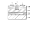
- FIGS. 1A and 1B show a cross-sectional structure of a gallium nitride based semiconductor device 100 according to one embodiment of the present invention.
- a gallium nitride based semiconductor device 100 has a structure in which a conductive alignment layer 104, a gallium nitride based semiconductor layer 106, and an upper electrode layer 108 are arranged on an amorphous substrate 102.
- FIG. Gallium nitride-based semiconductor device 100 further includes an auxiliary electrode layer 110 in contact with conductive alignment layer 104 .
- the conductive orientation layer 104 and the upper electrode layer 108 are used as electrodes, and the gallium nitride based semiconductor layer 106 is used as a functional layer for exhibiting a predetermined function.
- Predetermined functions depend on the structure of the device, but may include functions such as light emission, amplification, switching, and the like.
- a gallium nitride-based semiconductor device refers to a semiconductor device having a gallium nitride layer formed on an amorphous substrate and configured to exhibit a predetermined function.
- Gallium nitride based semiconductor devices may include light emitting devices such as light emitting diodes and active devices such as transistors.
- a gallium nitride-based semiconductor layer refers to a semiconductor layer including at least one gallium nitride layer, and may include a structure in which a plurality of gallium nitride layers having different conductivity types are laminated.
- a glass substrate is used as the amorphous substrate 102 .
- the glass substrate preferably has a low alkali component content, a low thermal expansion coefficient, a high strain point, and a high surface flatness.
- An alkali component is a component that is contained in a large amount in ordinary glass, and the glass substrate used in this embodiment preferably contains an alkali metal such as sodium in an amount of 0.1% or less.
- the glass substrate preferably has an expansion coefficient of less than 50 ⁇ 10 ⁇ 7 /° C. and a strain point of 600° C. or higher. Since the glass substrate does not contain an alkali component and has high heat resistance, a gallium nitride-based semiconductor layer having crystallinity can be formed by a sputtering method to form a semiconductor device, as will be described later.
- the amorphous substrate 102 is not required to have heat resistance of 1000° C. or more like the sapphire substrate. Rather, by using a glass substrate such as that used for liquid crystal displays and organic electroluminescence (organic EL) displays as the amorphous substrate 102, it is possible to fabricate a gallium nitride semiconductor device on a large-area glass substrate called mother glass. can be done. Also, as the amorphous substrate 102, a resin substrate such as a polyimide substrate, an acrylic substrate, a siloxane substrate, or a fluorine resin substrate may be used.
- an insulating layer may be provided on the surface of the amorphous substrate 102 .
- the insulating layer for example, a silicon nitride film, a silicon oxide film, an aluminum oxide film, or the like can be used.
- the insulating layer may be formed by stacking a plurality of types of insulating films, and may have a structure in which, for example, a silicon nitride film and a silicon oxide film are stacked.
- a conductive alignment layer 104 is provided on the amorphous substrate 102 .
- the conductive alignment layer 104 is a crystalline conductive film.
- the crystals of the conductive alignment layer 104 have an orientation, and the crystals are preferably oriented along the c-axis, for example.
- the conductive alignment layer 104 is preferably a crystal with rotational symmetry, for example, the crystal surface preferably has a 6-fold rotational symmetry.
- the conductive alignment layer 104 preferably has a hexagonal close-packed structure, a face-centered cubic structure, or similar structures.
- the structure conforming to the hexagonal close-packed structure or the face-centered cubic structure includes a crystal structure in which the c-axis is not 90 degrees with respect to the a-axis and the b-axis.
- the conductive alignment layer 104 using a conductive material having a hexagonal close-packed structure or similar structure is oriented in the (0001) direction, that is, in the c-axis direction with respect to the amorphous substrate 102 (hereinafter referred to as hexagonal close-packed structure). (0001) orientation of the dense structure is preferred.
- the conductive alignment layer 104 having a face-centered cubic structure or a similar structure is oriented in the (111) direction with respect to the amorphous substrate 102 (hereinafter referred to as the (111) orientation of the face-centered cubic structure). is preferred.
- a conductive alignment layer 104 is provided between the amorphous substrate 102 and the gallium nitride based semiconductor layer 106 .
- the gallium nitride-based semiconductor layer 106 preferably has crystallinity, and the conductive orientation layer 104 functions as a buffer layer. Since the conductive orientation layer 104 has the crystallinity as described above, the gallium nitride based semiconductor layer 106 grown thereon can be crystallized and the crystallization can be promoted.
- the conductive orientation layer 104 has a crystalline surface having six-fold rotational symmetry such as a hexagonal close-packed structure or a face-centered cubic structure, so that the c-axis of the gallium nitride-based semiconductor layer 106 grows in the film thickness direction. can be controlled to
- the crystallinity of the gallium nitride based semiconductor layer 106 is affected by the surface state of the conductive orientation layer 104 . Therefore, the conductive alignment layer 104 preferably has a flat surface. For example, the conductive alignment layer 104 preferably has a surface arithmetic mean roughness (Ra) of less than 2.3 nm. The crystallinity of the gallium nitride based semiconductor layer 106 can be enhanced by the conductive orientation layer 104 having a flat surface.
- the conductive alignment layer 104 is preferably a thin film in order to obtain a flat surface.
- the conductive alignment layer 104 preferably has a thickness of 100 nm or less, preferably 50 nm or less. By setting the film thickness of the conductive alignment layer 104 to 50 nm or less, a flat surface can be formed while maintaining crystallinity.
- the conductive alignment layer 104 preferably has conductivity so that it functions as an electrode of a gallium nitride-based semiconductor device.
- the conductive alignment layer 104 is preferably made of a metal material.
- the conductive alignment layer 104 is preferably made of titanium (Ti), aluminum (Al), and other metals such as silver (Ag), nickel (Ni), copper (Cu), strontium (Sr). , rhodium (Rh), palladium (Pd), iridium (Ir), platinum (Pt), gold (Au), and the like can be used.
- the conductive alignment layer 104 can also be made of conductive metal oxides such as zinc oxide (ZnO) and titanium dioxide (TiO 2 ).
- Such a conductive alignment layer 104 is produced by a sputtering method using a sputtering target made of a metal material for film formation.
- the conductive alignment layer 104 may be fabricated by a vacuum deposition method, an electron beam deposition method.
- the gallium nitride based semiconductor layer 106 includes at least one gallium nitride (GaN) layer.
- Gallium nitride is a compound of gallium (Ga) and nitrogen (N) and is a semiconductor.
- the gallium nitride layer preferably has a stoichiometric composition, but may deviate from the stoichiometric composition.
- the gallium nitride layer used as the gallium nitride based semiconductor layer 106 preferably has crystallinity.
- the crystallinity of the gallium nitride layer is preferably monocrystalline, but may be polycrystalline, microcrystalline, or nanocrystalline.
- the crystal structure of the gallium nitride layer preferably has a wurtzite structure.
- the gallium nitride layer used as the gallium nitride based semiconductor layer 106 preferably has c-axis orientation or (111) orientation.
- the conductivity type of the gallium nitride layer used as the gallium nitride based semiconductor layer 106 may be substantially intrinsic, or may have n-type conductivity or p-type conductivity.
- the gallium nitride layer having n-type conductivity may not contain a dopant for controlling valence electrons, or an element selected from silicon (Si) or germanium (Ge) as an n-type dopant. may be doped.
- the gallium nitride layer having p-type conductivity may be doped with an element selected from magnesium (Mg), zinc (Zn), cadmium (Cd), and beryllium (Be) as a p-type dopant.
- the n-type gallium nitride layer When the n-type gallium nitride layer is added with a dopant, it preferably has a carrier concentration of 1 ⁇ 10 18 /cm 3 or more.
- the p-type gallium nitride layer preferably has a carrier concentration of 5 ⁇ 10 16 /cm 3 or more when a dopant is added.
- the substantially intrinsic (in other words, highly resistive) gallium nitride layer may contain zinc (Zn) as a dopant.
- the gallium nitride layer used as the gallium nitride-based semiconductor layer 106 may contain one or more elements selected from indium (In), aluminum (Al), and arsenic (As). These elements can adjust the bandgap of the gallium nitride layer.
- a gallium nitride layer used as the gallium nitride based semiconductor layer 106 is provided on the conductive alignment layer 104 .
- the surface of the conductive orientation layer 104 (the surface in contact with the gallium nitride layer) contains a crystal plane with rotational symmetry or c-axis orientation, so that gallium nitride having c-axis orientation or (111) orientation layers are obtained.
- the gallium nitride layer may contain an amorphous structure near the interface in contact with the conductive alignment layer 104, but preferably has crystallinity in the bulk.
- the gallium nitride based semiconductor layer 106 having crystallinity can improve the performance of the gallium nitride based semiconductor device 100 . For example, if the gallium nitride-based semiconductor device 100 is a light-emitting device, the emission intensity can be increased, and if it is an active device such as a transistor, the carrier mobility can be increased.
- the gallium nitride based semiconductor layer 106 is deposited at a temperature below the strain point of the amorphous substrate 102 .
- a gallium nitride layer is generally formed by MOCVD (metal-organic chemical vapor deposition), but this film formation method requires a high process temperature, so considering the heat resistance of the amorphous substrate 102, it is not always suitable. I can't say In this embodiment, the gallium nitride-based semiconductor layer 106 is formed by a sputtering method that can be formed at a temperature below the strain point of the amorphous substrate 102 .
- a gallium nitride layer used as the gallium nitride-based semiconductor layer 106 is produced by sputtering while the amorphous substrate 102 is heated to 100 to 600.degree. Since the conductive orientation layer 104 is formed on the deposition surface of the amorphous substrate 102, a gallium nitride layer having crystallinity (preferably c-axis orientation) is formed by a sputtering method even at a substrate temperature of 600° C. or less. can grow.
- the gallium nitride layer used as the gallium nitride-based semiconductor layer 106 is sputtered using a gallium nitride sintered body as a sputtering target and using argon (Ar) or a mixed gas of argon (Ar) and nitrogen (N 2 ) as a sputtering gas. It is made by doing Various methods can be applied to the sputtering.
- a bipolar sputtering method a magnetron sputtering method, a dual magnetron sputtering method, a facing target sputtering method, an ion beam sputtering method, and an inductively coupled plasma (ICP) sputtering method can be applied.
- ICP inductively coupled plasma
- the film thickness of the gallium nitride-based semiconductor layer 106 is not limited, and is appropriately set according to the structure of the device.
- the gallium nitride-based semiconductor layer 106 may be a single layer, or may be a laminate of multiple layers having different conductivity types and/or compositions.
- the upper electrode layer 108 is provided on top of the gallium nitride based semiconductor layer 106 .
- the upper electrode layer 108 functions as an electrode for the gallium nitride based semiconductor device 100 .
- the upper electrode layer 108 is provided to form an ohmic contact with the gallium nitride based semiconductor layer 106 .
- the top electrode layer 108 may be omitted.
- the upper electrode layer 108 is made of a metal material such as aluminum (Al), titanium (Ti), platinum (Pt), nickel (Ni), tantalum (Ta).
- the upper electrode layer 108 may be formed of a metal oxide that has conductivity and is used as a transparent electrode, such as indium tin oxide (ITO), zinc oxide (ZnO), and indium zinc oxide (IZO). .
- the auxiliary electrode layer 110 is provided so as to be in contact with the conductive alignment layer 104 .
- FIG. 1A shows a structure in which an auxiliary electrode layer 110 is provided in contact with the upper surface (the surface facing the gallium nitride-based semiconductor layer 106) and side surfaces of the conductive alignment layer 104.
- FIG. 1B shows a structure in which the auxiliary electrode layer 110 is provided in contact with the lower surface of the conductive alignment layer 104 (the surface facing the amorphous substrate 102). As shown in FIGS. 1A and 1B, the outer peripheral portion of the conductive alignment layer 104 protrudes from the gallium nitride-based semiconductor layer 106, and the protruding portion is in contact with the auxiliary electrode layer 110, thereby increasing the contact area.
- the gallium nitride-based semiconductor layer 106 can be prevented from overlapping the stepped portion formed by the auxiliary electrode layer 110, thereby improving the crystallinity. can be made not to affect
- the auxiliary electrode layer 110 is formed with a thickness of 50 nm or more, preferably 100 nm to 1000 nm, in order to reduce electrical resistance. Therefore, as shown in FIG. 1B, when the auxiliary electrode layer 110 is brought into contact with the lower surface side of the conductive alignment layer 104, it is preferable that the ends have a tapered shape. Since the end of the auxiliary electrode layer 110 has a tapered shape in a cross-sectional view, the conductive alignment layer 104 can be prevented from being disconnected.
- FIGS. 1A and 1B only show a cross-sectional structure
- the auxiliary electrode layer 110 is preferably provided so as to surround the outer circumference of the conductive alignment layer 104 .
- an electrically connected state is formed.
- the conductive alignment layer 104 is used as an electrode of the gallium nitride based semiconductor device 100 .
- the conductive alignment layer 104 has a thickness of 50 nm or less as described above, an increase in electrode resistance becomes a problem.
- the resistivity of titanium (Ti) used as the conductive alignment layer 104 is 100 n ⁇ m, which is one order of magnitude higher than that of aluminum (Al). Therefore, when titanium (Ti) is used as the conductive alignment layer 104, there is concern that the resistance loss of the electrode may adversely affect the device characteristics.
- the gallium nitride-based semiconductor device 100 is a light-emitting device
- a problem may arise in that the light emission intensity becomes non-uniform in the plane. That is, when the conductive alignment layer 104 is connected to a power supply line, a phenomenon can occur in which the emission intensity decreases as the distance from the connection increases.
- the gallium nitride-based semiconductor device 100 shown in FIGS. 1A and 1B is provided with the auxiliary electrode layer 110, thereby solving the problem of the resistance loss of the conductive alignment layer 104.
- the auxiliary electrode layer 110 is electrically connected to the conductive alignment layer 104 and provided to reduce the surface resistivity of the conductive alignment layer 104, thereby eliminating the resistance loss problem. can do.
- the conductive alignment layer 104 can be used as it is as an electrode, and the influence of the high resistance of the electrode can be suppressed. can.
- auxiliary electrode layer 110 As the conductive material forming the auxiliary electrode layer 110 , metal materials such as aluminum (Al), titanium (Ti), silver (Ag), molybdenum (Mo), and tantalum (Ta) are used.
- the auxiliary electrode layer 110 is preferably thicker than the conductive alignment layer 104 for low resistance. Further, the auxiliary electrode layer 110 may have a structure (for example, Ti/Al/Ti) in which an aluminum (Al) film is sandwiched between high melting point metal films such as titanium (Ti) in order to improve heat resistance. good.
- the auxiliary electrode layer 110 is not limited to the structure shown in FIGS. 1A and 1B, and can be provided in various structures. Several embodiments of the auxiliary electrode layer 110 are illustrated below.
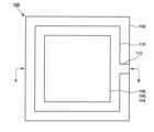
- FIG. 2A and 2B show the structure of a gallium nitride based semiconductor device 100 according to the second embodiment.
- FIG. 2A shows a plan view of a gallium nitride-based semiconductor device 100 according to this embodiment
- FIG. 2B shows a cross-sectional view corresponding to the line AB shown in FIG. 2A.
- the auxiliary electrode layer 110 is in contact with the side and top surfaces of the conductive alignment layer 104 and overlaps the gallium nitride based semiconductor layer 106 on the conductive alignment layer 104. have a structure.
- the auxiliary electrode layer 110 is provided so as to surround the outer periphery of the conductive alignment layer 104 .
- the auxiliary electrode layer 110 may be connected with the wiring 112 .
- the auxiliary electrode layer 110 may be formed of the same conductive layer as the conductive layer forming the wiring 112 . Forming the auxiliary electrode layer 110 and the wiring 112 from the same conductive layer eliminates the need for a connecting portion such as a contact hole, thereby simplifying the structure.
- the provision of the auxiliary electrode layer 110 suppresses deterioration of the characteristics of the gallium nitride-based semiconductor device 100 due to the high resistance of the conductive alignment layer 104. can do.
- the gallium nitride-based semiconductor device 100 is a light-emitting device, uneven brightness in the light-emitting region can be eliminated, and if it is an active device such as a transistor, an increase in power consumption can be suppressed.
- the size of the gallium nitride-based semiconductor device 100 can be reduced because the conductive alignment layer 104 does not need to have protrusions. As a result, the degree of integration can be increased when device integration is attempted.
- the crystallinity of the gallium nitride based semiconductor layer 106 is affected by the conductive orientation layer 104 . Since the auxiliary electrode layer 110 is a thick film and has a crystallinity different from that of the conductive orientation layer 104, there is concern that the gallium nitride based semiconductor layer 106 will be affected. Specifically, the crystallinity of the outer peripheral portion 114 of the gallium nitride based semiconductor layer 106 shown in FIGS. 2A and 2B may differ from the crystallinity of the region inside the outer peripheral portion 114 of the gallium nitride based semiconductor layer 106 .
- the outer peripheral portion 114 of the gallium nitride-based semiconductor layer 106 may be affected by the auxiliary electrode layer 110 and may be in an amorphous state with poorer crystallinity than the inner region. In this case, if the resistance of the outer peripheral portion 114 is increased, the leakage current flowing through the end surface of the gallium nitride based semiconductor layer 106 between the upper electrode layer 108 and the auxiliary electrode layer 110 can be reduced.
- the width over which the auxiliary electrode layer 110 overlaps the gallium nitride based semiconductor layer 106 is slightly smaller than the full width of the gallium nitride based semiconductor layer 106 . Therefore, as described above, even if a region with different crystallinity is formed in the outer peripheral portion 114, the effect on the gallium nitride based semiconductor device 100 is slight. Rather, by providing the gallium nitride-based semiconductor device 100 with the auxiliary electrode layer 110, it is possible to obtain the advantage of eliminating the influence of the conductive orientation layer 104 having a high resistance.
- the gallium nitride-based semiconductor device 100 is the same as that shown in the first embodiment, except that the auxiliary electrode layer 110 has a region overlapping the gallium nitride-based semiconductor layer 106, and obtains the same effects. be able to.
- FIG. 3A and 3B show the structure of a gallium nitride based semiconductor device 100 according to the third embodiment.
- FIG. 3A shows a plan view of a gallium nitride-based semiconductor device 100 according to this embodiment
- FIG. 3B shows a cross-sectional view corresponding to AB shown in FIG. 3A.
- the gallium nitride based semiconductor device 100 shown in FIGS. 3A and 3B has a structure in which the auxiliary electrode layer 110 is in contact with the lower surface of the conductive alignment layer 104 .
- the auxiliary electrode layer 110 is provided so as to surround the outer periphery of the conductive alignment layer 104 .
- the auxiliary electrode layer 110 may be connected to the wiring 112 , and the auxiliary electrode layer 110 may be formed of the same conductive layer as the conductive layer forming the wiring 112 .
- the structure in which the auxiliary electrode layer 110 is in contact with the lower surface of the conductive alignment layer 104 causes the gallium nitride-based semiconductor layer 106 to have a structure in which the entire lower surface thereof is in contact with the conductive alignment layer 104 . Therefore, the crystallinity of the gallium nitride based semiconductor layer 106 becomes uniform over the entire surface.
- the gallium nitride-based semiconductor layer 106 includes a portion that overlaps a step formed by the conductive alignment layer 104 overlapping the auxiliary electrode layer 110 . However, as in the second embodiment, the area of the stepped portion occupies a small proportion of the total area, and the effect on the gallium nitride based semiconductor device 100 is minor.
- the structure shown in FIGS. 3A and 3B can be said to be a structure in which the gallium nitride based semiconductor layer 106 is less susceptible to the formation of the auxiliary electrode layer than the structure shown in the first embodiment.
- the gallium nitride-based semiconductor device 100 according to this embodiment is the same as that shown in the second embodiment, except that the auxiliary electrode layer 110 is in contact with the lower surface of the conductive alignment layer 104, and the same effects can be obtained. can be done.
- FIG. 4A and 4B show the structure of a gallium nitride based semiconductor device 100 according to the fourth embodiment.
- 4A shows a plan view of a gallium nitride-based semiconductor device 100 according to this embodiment
- FIG. 4B shows a cross-sectional view corresponding to the line AB shown in FIG. 4A.
- the gallium nitride-based semiconductor device 100 shown in FIGS. 4A and 4B has a structure in which the auxiliary electrode layer 110 is in contact with the side surface of the conductive alignment layer 104 .
- the auxiliary electrode layer 110 may be in contact with the side surfaces of the gallium nitride based semiconductor layer 106 as well as the conductive alignment layer 104 .
- the auxiliary electrode layer 110 is preferably provided so as to be in contact with the outer peripheral side surfaces of the conductive alignment layer 104 and the gallium nitride based semiconductor layer 106 over the entire circumference.
- the gallium nitride-based semiconductor layer 106 may have a multilayer structure.
- the gallium nitride based semiconductor device 100 is a light emitting device
- the gallium nitride based semiconductor layer 106 is formed by laminating an n-type gallium nitride semiconductor layer, an active layer (light emitting layer), and a p-type gallium nitride semiconductor layer from the lower layer side. structure.
- the auxiliary electrode layer 110 is preferably provided so as to be in contact with the side surface of the n-type gallium nitride semiconductor layer, which is the bottom layer.
- the auxiliary electrode layer 110 shown in FIGS. 4A and 4B is formed after forming the gallium nitride based semiconductor layer 106 and the upper electrode layer 108 on the conductive alignment layer 104 . Specifically, after a laminate of a conductive alignment layer 104, a gallium nitride-based semiconductor layer 106, and an upper electrode layer 108 is formed on the amorphous substrate 102 as shown in FIG. A conductive film is formed to cover the top surface and side surfaces of the stack. Then, the auxiliary electrode layer 110 can be formed by etching back the conductive film by anisotropic etching so that the conductive layer remains on the side surface of the laminate.
- a conductive film for forming the auxiliary electrode layer 110 is made of a metal material such as titanium (Ti), aluminum (Al), silver (Ag), molybdenum (Mo), or tantalum (Ta).
- the auxiliary electrode layer 110 may be connected with traces 112 to connect with adjacent devices or power sources.
- the auxiliary electrode layer 110 By providing the auxiliary electrode layer 110 so as to be in contact with the side surface of the conductive alignment layer 104 in this way, it is possible to prevent the formation of the gallium nitride based semiconductor layer 106 from being affected.
- the gallium nitride based semiconductor layer 106 is formed on the conductive orientation layer 104, the upper electrode layer 108 is formed, and then the auxiliary electrode layer 110 is formed. It can be made not to affect the crystallinity. This makes it possible to obtain good device characteristics.
- the gallium nitride-based semiconductor device 100 according to this embodiment is the same as that shown in the first embodiment, except that the auxiliary electrode layer 110 is in contact with the side surface of the conductive alignment layer 104, and has the same effects. can be obtained.
- FIG. 5A and 5B show the structure of a gallium nitride based semiconductor device 100 according to the third embodiment.
- FIG. 5A shows a plan view of a gallium nitride-based semiconductor device 100 according to this embodiment
- FIG. 5B shows a cross-sectional view corresponding to AB shown in FIG. 5A.
- the gallium nitride-based semiconductor device 100 shown in FIGS. 5A and 5B has a structure in which the auxiliary electrode layer 110 is in contact with the entire bottom surface of the conductive alignment layer 104 .
- the auxiliary electrode layer 110 may have a structure continuous from the wiring 112 , and the auxiliary electrode layer 110 may be formed of the same conductive layer as the conductive layer forming the wiring 112 .
- the auxiliary electrode layer 110 may have a larger area than the conductive alignment layer 104 and may be edged outward.
- the auxiliary electrode layer 110 may have the same size as the conductive alignment layer 104 or a smaller area than the conductive alignment layer 104, and the ends thereof may be lined inside.
- the contact area can be increased, and the resistance can be more effectively reduced. . That is, the sheet resistance (surface resistance) of the conductive alignment layer 104 can be substantially reduced.
- the structure shown in FIGS. 5A and 5B has a structure in which the gallium nitride-based semiconductor layer 106 is in contact with the entire surface of the conductive orientation layer 104 . Therefore, the crystallinity of the gallium nitride based semiconductor layer 106 can be made uniform. In addition, if the area of the auxiliary electrode layer 110 is increased, the conductive alignment layer 104 does not have a stepped portion, so that the influence of the stepped portion can be eliminated. As described above, the structures shown in FIGS. 5A and 5B have structures in which the gallium nitride-based semiconductor layer 106 is less susceptible to the formation of the auxiliary electrode layer than the structures shown in the second and third embodiments. .
- the gallium nitride-based semiconductor device 100 according to this embodiment is the same as that shown in the first embodiment, except that the auxiliary electrode layer 110 is in contact with the lower surface of the conductive alignment layer 104, and the same effects can be obtained. can be done.
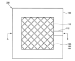
- FIG. 6A and 6B show the structure of a gallium nitride based semiconductor device 100 according to the sixth embodiment.
- FIG. 6A shows a plan view of a gallium nitride-based semiconductor device 100 according to this embodiment
- FIG. 6B shows a cross-sectional view corresponding to AB shown in FIG. 6A.
- the gallium nitride-based semiconductor device 100 shown in FIGS. 6A and 6B has a structure in which the auxiliary electrode layer 110 has a grid-like pattern and is provided on the upper surface of the conductive alignment layer 104 .
- the grid-like pattern of the auxiliary electrode layer 110 is provided to extend over the entire surface of the conductive alignment layer 104 .
- the auxiliary electrode layer 110 having a lattice pattern may be connected to the wiring 112 at the end.
- the auxiliary electrode layer 110 is formed of a metal material such as aluminum (Al), silver (Ag), etc., which has a lower resistance than the metal forming the conductive alignment layer 104 .
- the line width of the lattice pattern is narrowed so as to minimize the influence on the crystallinity of the gallium nitride based semiconductor layer 106 .
- the structure of the auxiliary electrode layer 110 shown in FIGS. 6A and 6B can substantially reduce the sheet resistance (surface resistance) of the conductive alignment layer 104.
- the lattice pattern of the auxiliary electrode layer 110 spreads over the entire surface of the conductive alignment layer 104, which is advantageous for increasing the area. For example, when the gallium nitride-based semiconductor device 100 is a light-emitting device, luminance unevenness (luminance gradient) can be suppressed even if the light-emitting region is enlarged.
- a gallium nitride-based semiconductor device 100 shown in FIGS. 7A and 7B has a structure in which an auxiliary electrode layer 110 having a grid-like pattern is provided so as to be in contact with the lower surface of a conductive alignment layer 104 .
- FIG. 7A shows a plan view of the gallium nitride-based semiconductor device 100 according to this embodiment
- FIG. 7B shows a cross-sectional view corresponding to AB shown in FIG. 7A.
- the auxiliary electrode layer 110 having a lattice pattern is provided between the amorphous substrate 102 and the conductive alignment layer 104 so that the entire surface of the gallium nitride based semiconductor layer 106 is in contact with the conductive alignment layer 104. and good crystallinity can be obtained.
- the lattice pattern of the auxiliary electrode layer 110 may be replaced with a stripe pattern or a mesh pattern.
- the configuration of the auxiliary electrode layer 110 shown in this embodiment can be appropriately combined with the auxiliary electrode layers shown in the first to fourth embodiments.
- the grid pattern shown in this embodiment is connected to the auxiliary electrode layer 110 arranged on the outer periphery of the conductive alignment layer 104 shown in the first embodiment, and the outer periphery of the conductive alignment layer 104 is connected.
- a configuration in which the auxiliary electrode layer 110 is provided in the portion and in the plane may be adopted.
- the gallium nitride-based semiconductor device 100 according to this embodiment is the same as that shown in the first embodiment, except that the auxiliary electrode layer 110 is in contact with the lower surface of the conductive alignment layer 104, and the same effects can be obtained. can be done.
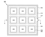
- FIG. 8A and 8B show the structure of a gallium nitride based semiconductor device 100 according to the seventh embodiment.
- 8A shows a plan view of a gallium nitride-based semiconductor device 100 according to this embodiment
- FIG. 8B shows a cross-sectional view corresponding to the line AB shown in FIG. 8A.
- FIG. 8A and 8B show a gallium nitride based semiconductor device 100 in which a plurality of stacked stacks 116 of conductive alignment layers 104, gallium nitride based semiconductor layers 106, and top electrode layers 108 are disposed on an amorphous substrate 102.
- Each laminate 116 has the structure shown in the second embodiment.
- a plurality of laminates 116 are spaced apart on the amorphous substrate 102, and an auxiliary electrode layer 110 is provided in a region where the plurality of laminates 116 are spaced apart.
- the auxiliary electrode layer 110 is provided to connect adjacent laminates 116 .
- the auxiliary electrode layer 110 is arranged so as to spread over the entire region where the multiple laminates 116 are arranged. With such an arrangement, it is possible not only to electrically connect the plurality of stacked bodies 116 but also to reduce the resistance.
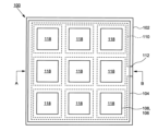
- FIGS. 9A and 9B show the case where each of the plurality of laminates 116 has the same structure as the structure shown in the third embodiment.
- FIG. 9A shows a plan view of the gallium nitride-based semiconductor device 100
- FIG. 9B shows a cross-sectional view corresponding to the line AB shown in FIG. 9A.
- the configuration in which the auxiliary electrode layer 110 is arranged on the lower layer side of the conductive alignment layer 104 can also connect adjacent stacks 116 .
- FIGS. 8A and 8B and 9A and 9B show an example in which all of the conductive alignment layers 104 of the multiple laminates 116 are connected to the same potential, but the configuration of the auxiliary electrode layer 110 is shown. is not limited to the examples.
- a structure in which the auxiliary electrode layer 110 is provided so that the plurality of laminates 116 arranged in a matrix are connected in the row direction or the column direction, and the plurality of laminates 116 are connected in series and parallel on the amorphous substrate 102. may be formed.
- the gallium nitride-based semiconductor device 100 shown in this embodiment is advantageous, for example, in realizing a relatively large-area light-emitting device.
- the plurality of laminates 116 do not need to increase the area of each, can prevent luminance unevenness due to the resistance of the conductive alignment layer 104, and can achieve low resistance by the auxiliary electrode layer 110.
- FIG. As a result, it is possible to obtain a light-emitting device having a uniform luminance distribution during light emission.
- FIG. 10A and 10B show the structure of a gallium nitride based semiconductor device 100 according to the eighth embodiment.
- FIG. 10A shows a plan view of a gallium nitride-based semiconductor device 100 according to this embodiment
- FIG. 10B shows a cross-sectional view corresponding to AB shown in FIG. 10A.
- a gallium nitride-based semiconductor device 100 shown in FIGS. 10A and 10B has a configuration in which a plurality of laminated bodies 118 are provided as in the seventh embodiment, but the structure of the conductive orientation layer 104 is different.
- the conductive alignment layer 104 is continuous and has a structure commonly provided over a plurality of laminates 118 .
- the gallium nitride-based semiconductor device 100 according to the present embodiment has a conductive orientation layer 104 provided on an amorphous substrate 102, and a plurality of divided gallium nitride-based semiconductor layers and upper electrodes are formed thereon. is arranged.
- the auxiliary electrode layer 110 is provided so as to be in contact with the upper surface of the conductive alignment layer 104 in a region where the gallium nitride-based semiconductor layer 106 divided into a plurality of parts is separated.
- the auxiliary electrode layer 110 is provided on the conductive alignment layer 104 in a lattice pattern, and the gallium nitride based semiconductor layer 106 and the upper electrode layer 108 are formed in the openings of the lattice. pattern is placed.
- the thickness of the auxiliary electrode layer 110 can be increased, and the resistance of the auxiliary electrode of the conductive alignment layer 104 can be reduced.
- FIGS. 11A and 11B show a structure in which the auxiliary electrode layer 110 is provided on the lower layer side of the conductive alignment layer 104.
- FIG. 11A shows a plan view of the gallium nitride-based semiconductor device 100
- FIG. 11B shows a cross-sectional view corresponding to AB shown in FIG. 11A.
- a configuration in which the auxiliary electrode layer 110 is arranged on the lower layer side of the conductive alignment layer 104 can also achieve low resistance.
- the gallium nitride-based semiconductor device 100 shown in this embodiment is advantageous in realizing a relatively large-area light-emitting device, as in the seventh embodiment. It is not necessary to increase the area of each light emitting region, and the provision of the auxiliary electrode layer 110 can prevent luminance unevenness caused by the resistance of the conductive alignment layer 104 . This makes it possible to obtain a light-emitting device with a uniform luminance distribution during light emission.
- FIG. 12A shows the configuration of the gallium nitride based semiconductor layer 106 when the gallium nitride based semiconductor device 100 is a light emitting device.
- the gallium nitride based semiconductor layer 106 has a structure in which an n-type gallium nitride layer 120 , a light emitting layer 124 and a p-type gallium nitride layer 130 are laminated on the conductive alignment layer 104 .
- An upper electrode layer 108 is provided on the p-type gallium nitride layer 130 .
- the upper electrode layer 108 is made of a metal material such as gold (Au), a titanium (Ti)-gold (Au) alloy, or a transparent conductive film such as indium tin oxide (ITO).
- the structure of the light emitting layer 124 may vary, and may be formed by quantum well layers in which gallium nitride (GaN) layers and indium gallium nitride (InGaN) layers are alternately stacked.
- FIG. 12B shows another configuration of the gallium nitride based semiconductor layer 106 included in the light emitting device.
- 12B has a structure in which an n-type gallium nitride layer 120, an n-type aluminum gallium nitride layer 122, an indium gallium nitride layer 126, a p-type aluminum gallium nitride layer 128, and a p-type gallium nitride layer 130 are laminated.
- Each of these layers is produced by a sputtering method. Since each layer has a different composition, it is formed using a sputtering target containing a dopant corresponding to each conductivity type.
- n-type dopant an element selected from silicon (Si) and germanium (Ge) can be used, and as a p-type dopant, magnesium (Mg), zinc (Zn), and cadmium (Cd) can be used. , and beryllium (Be). Since these layers are preferably formed continuously in vacuum, a multi-chamber sputtering apparatus is used.
- FIG. 13 shows the configuration of the gallium nitride based semiconductor layer 106 when the gallium nitride based semiconductor device 100 is a transistor.
- the gallium nitride-based semiconductor layer 106 has a structure in which an n + -type gallium nitride layer 132, an n-type gallium nitride layer 134, a p-type gallium nitride layer 136, and an n-type gallium nitride layer 138 are laminated on the conductive orientation layer 104.
- a source electrode 140 is provided on the n-type gallium nitride layer 138 and the conductive alignment layer 104 is used as the drain electrode.
- the gate electrode 142 has a trench gate structure and is provided so as to be embedded in the p-type gallium nitride layer 130 via the gate insulating layer 144 .
- Each layer of the gallium nitride based semiconductor layer 106 is produced by a sputtering method.
- the configuration of the gallium nitride based semiconductor layer 106 shown in this embodiment can be applied to the configurations shown in the first to eighth embodiments. As shown in FIGS. 12A, 12B, and 13, the gallium nitride-based semiconductor layer 106 can have various laminated structures, and devices can be configured according to applications.
- FIG. 14 is a schematic diagram showing the configuration of a light emitting device 150 according to an embodiment of the invention.
- a light-emitting device 150 has a pixel portion 152 and a terminal portion 154 formed on an amorphous substrate 102 .
- the pixel portion 152 is formed in the central portion of the amorphous substrate 102 and the terminal portion 154 is formed in the edge portion of the amorphous substrate 102 .
- the pixel portion 152 includes a plurality of pixels 156 arranged in a matrix. Each of the plurality of pixels 156 is provided with a light-emitting device having the structure shown in the first to sixth embodiments.
- Terminal portion 154 includes a plurality of terminals 158 .
- a power supply line is connected to each of the plurality of terminals 158 so that voltage can be applied (current can be supplied) to the light emitting device in the pixel 156 .
- a transistor may be provided in the pixel 156 and light emission of the light emitting device may be controlled by the transistor.
- 100 gallium nitride based semiconductor device, 102: amorphous substrate, 104: conductive orientation layer, 106: gallium nitride based semiconductor layer, 108: upper electrode layer, 110: auxiliary electrode layer, 112: wiring, 114: peripheral portion, 116 : laminated body 118: laminated body 120: n-type gallium nitride layer 122: n-type aluminum gallium nitride layer 124: light emitting layer 126: indium gallium nitride layer 128: p-type aluminum gallium nitride layer 130: p type gallium nitride layer, 132: n + type gallium nitride layer, 134: n type gallium nitride layer, 136: p type gallium nitride layer, 138: n type gallium nitride layer, 140: source electrode, 142: gate electrode, 144: Gate insulating layer 150: light emitting device 152: pixel
Abstract
This gallium nitride-based semiconductor device includes an amorphous substrate, a conductive alignment layer on the amorphous substrate, a gallium nitride-based semiconductor layer on the conductive alignment layer, and an auxiliary electrode layer in contact with the conductive alignment layer. The conductive alignment layer is preferably a c-axis oriented metal film or metal oxide film, and the auxiliary electrode layer is provided so as to surround the outer periphery of the conductive alignment layer.
Description
本発明の一実施形態は、アモルファス基板上の結晶性化合物半導体層を含む半導体デバイスに関する。
One embodiment of the present invention relates to a semiconductor device including a crystalline compound semiconductor layer on an amorphous substrate.
結晶性サファイア基板上に有機金属化合物気相成長法(MOCVD法)により窒化ガリウム系化合物半導体を気相成長させて形成された窒化ガリウム系化合物半導体発光ダイオードが知られている(特許文献1参照)。結晶正サファイア基板上の窒化ガリウム系化合物半導体発光ダイオードは青色発光を実現し、高い変換効率と長寿命を有し、広く実用化されている。しかし、結晶性サファイア基板は高価であり大面積化も容易でないことから、アモルファス基板上に結晶性を有する窒化ガリウム系化合物半導体を作製する研究が進められている(特許文献2、非特許文献1参照)。
A gallium nitride-based compound semiconductor light-emitting diode is known which is formed by vapor-growing a gallium nitride-based compound semiconductor on a crystalline sapphire substrate by a metal-organic chemical vapor deposition method (MOCVD method) (see Patent Document 1). . Gallium nitride-based compound semiconductor light-emitting diodes on crystalline sapphire substrates have realized blue light emission, have high conversion efficiency and long life, and have been widely put into practical use. However, since crystalline sapphire substrates are expensive and it is not easy to increase the area, research is underway to fabricate crystalline gallium nitride-based compound semiconductors on amorphous substrates (Patent Document 2, Non-Patent Document 1). reference).
窒化ガリウム層を用いて発光デバイスを作製する場合、金属層の上に窒化ガリウム層を設け、当該金属層を電極として用いることができれば便利である。しかし、窒化ガリウム層の下地側に配置する金属層は、材質、膜厚に制約があるため、そのまま電極として用いることが困難である。すなわち、発光デバイスがアモルファス基板に形成される場合、電源線との接続部近傍では明るく発光するものの、電源との接続部から離れるに従い輝度が低下して暗くなることが懸念される。
When fabricating a light-emitting device using a gallium nitride layer, it is convenient if the gallium nitride layer can be provided on the metal layer and the metal layer can be used as an electrode. However, it is difficult to use the metal layer placed on the underlying side of the gallium nitride layer as an electrode as it is because there are restrictions on the material and thickness of the metal layer. That is, when a light-emitting device is formed on an amorphous substrate, there is a concern that although it emits light brightly in the vicinity of the connection with the power supply line, the luminance decreases and becomes darker away from the connection with the power supply.
このような問題に鑑み本発明の一実施形態は、アモルファス基板上の窒化ガリウム系半導体層を用いた半導体デバイスにおいて、発光強度の面内均一性を図ることを目的の一つとする。
In view of such problems, one object of one embodiment of the present invention is to achieve in-plane uniformity of emission intensity in a semiconductor device using a gallium nitride-based semiconductor layer on an amorphous substrate.
本発明の一実施形態に係る窒化ガリウム系半導体デバイスは、アモルファス基板と、アモルファス基板上の導電性配向層と、導電性配向層上の窒化ガリウム系半導体層と、導電性配向層に接する補助電極層と、を含む。
A gallium nitride-based semiconductor device according to one embodiment of the present invention includes an amorphous substrate, a conductive alignment layer on the amorphous substrate, a gallium nitride-based semiconductor layer on the conductive alignment layer, and an auxiliary electrode in contact with the conductive alignment layer. and a layer.
以下、本発明の実施の形態を、図面等を参照しながら説明する。但し、本発明は多くの異なる態様で実施することが可能であり、以下に例示する実施の形態の記載内容に限定して解釈されるものではない。図面は説明をより明確にするため、実際の態様に比べ、各部の幅、厚さ、形状等について模式的に表される場合があるが、あくまで一例であって、本発明の解釈を限定するものではない。また、本明細書と各図において、既出の図に関して前述したものと同様の要素には、同一の符号(又は数字の後にa、bなどを付した符号)を付して、詳細な説明を適宜省略することがある。さらに各要素に対する「第1」、「第2」と付記された文字は、各要素を区別するために用いられる便宜的な標識であり、特段の説明がない限りそれ以上の意味を有しない。
Hereinafter, embodiments of the present invention will be described with reference to the drawings. However, the present invention can be implemented in many different aspects and should not be construed as being limited to the description of the embodiments exemplified below. In order to make the description clearer, the drawings may schematically show the width, thickness, shape, etc. of each part compared to the actual embodiment, but this is only an example and limits the interpretation of the present invention. not a thing In addition, in this specification and each figure, the same reference numerals (or numerals followed by a, b, etc.) are attached to the same elements as those described above with respect to the previous figures, and a detailed description is given. It may be omitted as appropriate. Further, the letters "first" and "second" for each element are convenient labels used to distinguish each element and have no further meaning unless otherwise specified.
本明細書において、ある部材又は領域が他の部材又は領域の「上に(又は下に)」あるとする場合、特段の限定がない限りこれは他の部材又は領域の直上(又は直下)にある場合のみでなく他の部材又は領域の上方(又は下方)にある場合を含み、すなわち、他の部材又は領域の上方(又は下方)において間に別の構成要素が含まれている場合も含む。
In this specification, when a member or region is “above (or below)” another member or region, it means directly above (or directly below) the other member or region unless otherwise specified. Includes not only one case but also the case above (or below) another member or region, that is, the case where another component is included between above (or below) another member or region .
[第1実施形態]
図1A及び図1Bは、本発明の一実施形態に係る窒化ガリウム系半導体デバイス100の断面構造を示す。図1A及び図1Bに示すように、窒化ガリウム系半導体デバイス100は、アモルファス基板102の上に、導電性配向層104、窒化ガリウム系半導体層106、上部電極層108が配置された構造を有する。窒化ガリウム系半導体デバイス100は、さらに、導電性配向層104に接触する補助電極層110を含む。 [First Embodiment]
1A and 1B show a cross-sectional structure of a gallium nitride basedsemiconductor device 100 according to one embodiment of the present invention. As shown in FIGS. 1A and 1B, a gallium nitride based semiconductor device 100 has a structure in which a conductive alignment layer 104, a gallium nitride based semiconductor layer 106, and an upper electrode layer 108 are arranged on an amorphous substrate 102. FIG. Gallium nitride-based semiconductor device 100 further includes an auxiliary electrode layer 110 in contact with conductive alignment layer 104 .
図1A及び図1Bは、本発明の一実施形態に係る窒化ガリウム系半導体デバイス100の断面構造を示す。図1A及び図1Bに示すように、窒化ガリウム系半導体デバイス100は、アモルファス基板102の上に、導電性配向層104、窒化ガリウム系半導体層106、上部電極層108が配置された構造を有する。窒化ガリウム系半導体デバイス100は、さらに、導電性配向層104に接触する補助電極層110を含む。 [First Embodiment]
1A and 1B show a cross-sectional structure of a gallium nitride based
窒化ガリウム系半導体デバイス100において、導電性配向層104及び上部電極層108は電極として用いられ、窒化ガリウム系半導体層106は所定の機能を発現させるための機能層として用いられる。所定の機能はデバイスの構造により変わるものであるが、例えば、発光、増幅、スイッチングなどの機能が含まれ得る。
In the gallium nitride based semiconductor device 100, the conductive orientation layer 104 and the upper electrode layer 108 are used as electrodes, and the gallium nitride based semiconductor layer 106 is used as a functional layer for exhibiting a predetermined function. Predetermined functions depend on the structure of the device, but may include functions such as light emission, amplification, switching, and the like.
なお、本明細書において、窒化ガリウム系半導体デバイスとは、アモルファス基板上に形成された窒化ガリウム層を有し、所定の機能を発現するように構成された半導体デバイスを指すものとする。窒化ガリウム系半導体デバイスには、発光ダイオードのような発光デバイス、トランジスタのような能動デバイスが含まれ得る。また、窒化ガリウム系半導体層は、少なくとも1層の窒化ガリウム層を含む半導体層を指し、導電型の異なる複数の窒化ガリウム層が積層された構造を含む場合もある。
In this specification, a gallium nitride-based semiconductor device refers to a semiconductor device having a gallium nitride layer formed on an amorphous substrate and configured to exhibit a predetermined function. Gallium nitride based semiconductor devices may include light emitting devices such as light emitting diodes and active devices such as transistors. A gallium nitride-based semiconductor layer refers to a semiconductor layer including at least one gallium nitride layer, and may include a structure in which a plurality of gallium nitride layers having different conductivity types are laminated.
次に、図1A及び図1Bに示す、窒化ガリウム系半導体デバイス100を構成する各部の詳細について説明する。
Next, details of each part constituting the gallium nitride based semiconductor device 100 shown in FIGS. 1A and 1B will be described.
アモルファス基板102としてガラス基板が用いられる。ガラス基板は、アルカリ成分の含有率が低く、熱膨張係数が低く、歪み点が高く、表面の平坦性が高いことが好ましい。アルカリ成分は通常のガラスの中に多く含まれる成分であるが、本実施形態で用いるガラス基板としては、ナトリウムのようなアルカリ金属が0.1%以下であることが好ましい。また、ガラス基板は、膨張係数が50×10-7/℃より小さく、歪み点が600℃以上であることが好ましい。ガラス基板が、アルカリ成分を含まず、高い耐熱性を有することで、後述されるように、スパッタリング法で結晶性を有する窒化ガリウム系半導体層を成膜し、半導体デバイスを形成することができる。
A glass substrate is used as the amorphous substrate 102 . The glass substrate preferably has a low alkali component content, a low thermal expansion coefficient, a high strain point, and a high surface flatness. An alkali component is a component that is contained in a large amount in ordinary glass, and the glass substrate used in this embodiment preferably contains an alkali metal such as sodium in an amount of 0.1% or less. The glass substrate preferably has an expansion coefficient of less than 50×10 −7 /° C. and a strain point of 600° C. or higher. Since the glass substrate does not contain an alkali component and has high heat resistance, a gallium nitride-based semiconductor layer having crystallinity can be formed by a sputtering method to form a semiconductor device, as will be described later.
尤も、アモルファス基板102には、サファイア基板のような1000℃以上の耐熱性は要求されない。むしろ、アモルファス基板102として、液晶ディスプレイや有機エレクトロルミネセンス(有機EL)ディスプレイに使用されるようなガラス基板を用いることで、マザーガラスと呼ばれる大面積ガラス基板に窒化ガリウム系半導体デバイスを作製することができる。また、アモルファス基板102として、ポリイミド基板、アクリル基板、シロキサン基板、フッ素樹脂基板などの樹脂基板が用いられてもよい。
However, the amorphous substrate 102 is not required to have heat resistance of 1000° C. or more like the sapphire substrate. Rather, by using a glass substrate such as that used for liquid crystal displays and organic electroluminescence (organic EL) displays as the amorphous substrate 102, it is possible to fabricate a gallium nitride semiconductor device on a large-area glass substrate called mother glass. can be done. Also, as the amorphous substrate 102, a resin substrate such as a polyimide substrate, an acrylic substrate, a siloxane substrate, or a fluorine resin substrate may be used.
図1A及び図1Bには図示されないが、アモルファス基板102の表面に絶縁層が設けられてもよい。絶縁層として、例えば、窒化シリコン膜、酸化シリコン膜、酸化アルミニウム膜などを用いることができる。また、絶縁層は、複数種の絶縁膜が積層されていてもよく、例えば、窒化シリコン膜と酸化シリコン膜とが積層された構造を有していてもよい。
Although not shown in FIGS. 1A and 1B, an insulating layer may be provided on the surface of the amorphous substrate 102 . As the insulating layer, for example, a silicon nitride film, a silicon oxide film, an aluminum oxide film, or the like can be used. Further, the insulating layer may be formed by stacking a plurality of types of insulating films, and may have a structure in which, for example, a silicon nitride film and a silicon oxide film are stacked.
導電性配向層104はアモルファス基板102の上に設けられる。導電性配向層104は、結晶性を有する導電膜である。導電性配向層104の結晶は配向性を有し、その結晶は、例えばc軸に配向していることが好ましい。導電性配向層104は回転対称性を有する結晶であることが好ましく、例えば、その結晶表面が6回回転対称を有することが好ましい。例えば、導電性配向層104は、六方最密構造、面心立方構造、又はこれらに準ずる構造を有することが好ましい。ここで、六方最密構造又は面心立方構造に準ずる構造とは、a軸およびb軸に対してc軸が90度とならない結晶構造を含む。六方最密構造又はこれに準ずる構造を有する導電性材料を用いた導電性配向層104は、アモルファス基板102に対して(0001)方向、すなわち、c軸方向に配向している(以下、六方最密構造の(0001)配向という)ことが好ましい。また、面心立方構造またはこれに準ずる構造を有する導電性配向層104は、アモルファス基板102に対して(111)方向に配向している(以下、面心立方構造の(111)配向という)ことが好ましい。
A conductive alignment layer 104 is provided on the amorphous substrate 102 . The conductive alignment layer 104 is a crystalline conductive film. The crystals of the conductive alignment layer 104 have an orientation, and the crystals are preferably oriented along the c-axis, for example. The conductive alignment layer 104 is preferably a crystal with rotational symmetry, for example, the crystal surface preferably has a 6-fold rotational symmetry. For example, the conductive alignment layer 104 preferably has a hexagonal close-packed structure, a face-centered cubic structure, or similar structures. Here, the structure conforming to the hexagonal close-packed structure or the face-centered cubic structure includes a crystal structure in which the c-axis is not 90 degrees with respect to the a-axis and the b-axis. The conductive alignment layer 104 using a conductive material having a hexagonal close-packed structure or similar structure is oriented in the (0001) direction, that is, in the c-axis direction with respect to the amorphous substrate 102 (hereinafter referred to as hexagonal close-packed structure). (0001) orientation of the dense structure is preferred. In addition, the conductive alignment layer 104 having a face-centered cubic structure or a similar structure is oriented in the (111) direction with respect to the amorphous substrate 102 (hereinafter referred to as the (111) orientation of the face-centered cubic structure). is preferred.
導電性配向層104は、アモルファス基板102と窒化ガリウム系半導体層106との間に設けられる。窒化ガリウム系半導体層106は結晶性を有することが好ましく、導電性配向層104は緩衝層としての機能を有する。導電性配向層104が上記のような結晶性を有することにより、この上に成長される窒化ガリウム系半導体層106の結晶化を図り、また結晶化を促進することができる。すなわち、導電性配向層104が、六方最密構造又は面心立方構造のような6回回転対称を有する結晶性表面を有することで、窒化ガリウム系半導体層106のc軸が膜厚方向に成長するように制御することができる。
A conductive alignment layer 104 is provided between the amorphous substrate 102 and the gallium nitride based semiconductor layer 106 . The gallium nitride-based semiconductor layer 106 preferably has crystallinity, and the conductive orientation layer 104 functions as a buffer layer. Since the conductive orientation layer 104 has the crystallinity as described above, the gallium nitride based semiconductor layer 106 grown thereon can be crystallized and the crystallization can be promoted. That is, the conductive orientation layer 104 has a crystalline surface having six-fold rotational symmetry such as a hexagonal close-packed structure or a face-centered cubic structure, so that the c-axis of the gallium nitride-based semiconductor layer 106 grows in the film thickness direction. can be controlled to
さらに、窒化ガリウム系半導体層106の結晶性は、導電性配向層104の表面状態の影響を受ける。そのため、導電性配向層104は、平坦な表面を有することが好ましい。例えば、導電性配向層104は、表面の算術平均粗さ(Ra)が2.3nmより小さいことが好ましい。導電性配向層104が平坦な表面を有することにより、窒化ガリウム系半導体層106の結晶性を高めることができる。
Furthermore, the crystallinity of the gallium nitride based semiconductor layer 106 is affected by the surface state of the conductive orientation layer 104 . Therefore, the conductive alignment layer 104 preferably has a flat surface. For example, the conductive alignment layer 104 preferably has a surface arithmetic mean roughness (Ra) of less than 2.3 nm. The crystallinity of the gallium nitride based semiconductor layer 106 can be enhanced by the conductive orientation layer 104 having a flat surface.
導電性配向層104は、平坦な表面を得るために、薄膜であることが好ましい。例えば、導電性配向層104の膜厚は、100nm以下、好ましくは50nm以下の膜厚を有することが好ましい。導電性配向層104の膜厚を50nm以下とすることで、結晶性を有しつつ、平坦な表面を形成することができる。
The conductive alignment layer 104 is preferably a thin film in order to obtain a flat surface. For example, the conductive alignment layer 104 preferably has a thickness of 100 nm or less, preferably 50 nm or less. By setting the film thickness of the conductive alignment layer 104 to 50 nm or less, a flat surface can be formed while maintaining crystallinity.
導電性配向層104は、窒化ガリウム系半導体デバイスの電極として機能させるため、導電性を有することが好ましい。電極としての機能を実現するため、導電性配向層104は金属材料で形成されることが好ましい。例えば、導電性配向層104は、チタン(Ti)、アルミニウム(Al)で形成されることが好ましく、その他の金属として、銀(Ag)、ニッケル(Ni)、銅(Cu)、ストロンチウム(Sr)、ロジウム(Rh)、パラジウム(Pd)、イリジウム(Ir)、白金(Pt)、金(Au)などを用いることができる。また、導電性配向層104は、酸化亜鉛(ZnO)、二酸化チタン(TiO2)などの導電性金属酸化物を用いることもできる。
The conductive alignment layer 104 preferably has conductivity so that it functions as an electrode of a gallium nitride-based semiconductor device. In order to function as an electrode, the conductive alignment layer 104 is preferably made of a metal material. For example, the conductive alignment layer 104 is preferably made of titanium (Ti), aluminum (Al), and other metals such as silver (Ag), nickel (Ni), copper (Cu), strontium (Sr). , rhodium (Rh), palladium (Pd), iridium (Ir), platinum (Pt), gold (Au), and the like can be used. The conductive alignment layer 104 can also be made of conductive metal oxides such as zinc oxide (ZnO) and titanium dioxide (TiO 2 ).
このような導電性配向層104は、成膜する金属材料で形成されたスパッタリングターゲットを用い、スパッタリング法で作製される。また、導電性配向層104は、真空蒸着法、電子ビーム蒸着法で作製されてもよい。
Such a conductive alignment layer 104 is produced by a sputtering method using a sputtering target made of a metal material for film formation. Alternatively, the conductive alignment layer 104 may be fabricated by a vacuum deposition method, an electron beam deposition method.
窒化ガリウム系半導体層106は、少なくとも一層の窒化ガリウム(GaN)層を含む。窒化ガリウムは、ガリウム(Ga)と窒素(N)の化合物であり、半導体である。窒化ガリウム層は化学量論的組成を有していることが好ましいが、化学量論的組成からずれていてもよい。窒化ガリウム系半導体層106として用いられる窒化ガリウム層は、結晶性を有していることが好ましい。窒化ガリウム層の結晶性は、単結晶であることが好ましいが、多結晶、微結晶、又はナノ結晶であってもよい。窒化ガリウム層の結晶構造は、ウルツ鉱構造を有することが好ましい。窒化ガリウム系半導体層106として用いられる窒化ガリウム層は、c軸配向又は(111)配向を有していることが好ましい。
The gallium nitride based semiconductor layer 106 includes at least one gallium nitride (GaN) layer. Gallium nitride is a compound of gallium (Ga) and nitrogen (N) and is a semiconductor. The gallium nitride layer preferably has a stoichiometric composition, but may deviate from the stoichiometric composition. The gallium nitride layer used as the gallium nitride based semiconductor layer 106 preferably has crystallinity. The crystallinity of the gallium nitride layer is preferably monocrystalline, but may be polycrystalline, microcrystalline, or nanocrystalline. The crystal structure of the gallium nitride layer preferably has a wurtzite structure. The gallium nitride layer used as the gallium nitride based semiconductor layer 106 preferably has c-axis orientation or (111) orientation.
窒化ガリウム系半導体層106として用いられる窒化ガリウム層の導電型は、実質的に真性であってもよいし、n型の導電性又はp型の導電性を有していてもよい。n型の導電性を有する窒化ガリウム層は、価電子制御を行うためのドーパントが含まれていなくてもよいし、n型ドーパントとしてシリコン(Si)又はゲルマニウム(Ge)から選ばれた一種の元素がドーピングされていてもよい。p型の導電性を有する窒化ガリウム層は、p型ドーパントとしてマグネシウム(Mg)、亜鉛(Zn)、カドミウム(Cd)、ベリリウム(Be)から選ばれた一種の元素がドーピングされていてもよい。n型の窒化ガリウム層は、ドーパントと添加する場合、1×10¹⁸/cm3以上のキャリア濃度を有していることが好ましい。p型の窒化ガリウム層は、ドーパントを添加する場合、5×1016/cm3以上のキャリア濃度を有していることが好ましい。また、実質的に真性(別言すれば、高抵抗である)窒化ガリウム層は、ドーパントとして亜鉛(Zn)が含まれていてもよい。
The conductivity type of the gallium nitride layer used as the gallium nitride based semiconductor layer 106 may be substantially intrinsic, or may have n-type conductivity or p-type conductivity. The gallium nitride layer having n-type conductivity may not contain a dopant for controlling valence electrons, or an element selected from silicon (Si) or germanium (Ge) as an n-type dopant. may be doped. The gallium nitride layer having p-type conductivity may be doped with an element selected from magnesium (Mg), zinc (Zn), cadmium (Cd), and beryllium (Be) as a p-type dopant. When the n-type gallium nitride layer is added with a dopant, it preferably has a carrier concentration of 1×10 18 /cm 3 or more. The p-type gallium nitride layer preferably has a carrier concentration of 5×10 16 /cm 3 or more when a dopant is added. Also, the substantially intrinsic (in other words, highly resistive) gallium nitride layer may contain zinc (Zn) as a dopant.
窒化ガリウム系半導体層106として用いられる窒化ガリウム層には、インジウム(In)、アルミニウム(Al)、ヒ素(As)から選ばれた一種又は複数種の元素が含まれていてもよい。これらの元素によって、窒化ガリウム層のバンドギャップを調整することができる。
The gallium nitride layer used as the gallium nitride-based semiconductor layer 106 may contain one or more elements selected from indium (In), aluminum (Al), and arsenic (As). These elements can adjust the bandgap of the gallium nitride layer.
窒化ガリウム系半導体層106として用いられる窒化ガリウム層は、導電性配向層104の上に設けられる。前述のように、導電性配向層104の表面(窒化ガリウム層と接する面)が、回転対称性、又はc軸配向した結晶面を含むことで、c軸配向又は(111)配向を有する窒化ガリウム層が得られる。窒化ガリウム層は、導電性配向層104と接する界面近傍にアモルファス構造が含まれてもよいが、バルクでは結晶性を有していることが好ましい。窒化ガリウム系半導体層106が結晶性を有することで、窒化ガリウム系半導体デバイス100の性能を高めることができる。例えば、窒化ガリウム系半導体デバイス100が発光デバイスである場合には発光強度を高めることができ、トランジスタのような能動デバイスの場合にはキャリア移動度を高めることができる。
A gallium nitride layer used as the gallium nitride based semiconductor layer 106 is provided on the conductive alignment layer 104 . As described above, the surface of the conductive orientation layer 104 (the surface in contact with the gallium nitride layer) contains a crystal plane with rotational symmetry or c-axis orientation, so that gallium nitride having c-axis orientation or (111) orientation layers are obtained. The gallium nitride layer may contain an amorphous structure near the interface in contact with the conductive alignment layer 104, but preferably has crystallinity in the bulk. The gallium nitride based semiconductor layer 106 having crystallinity can improve the performance of the gallium nitride based semiconductor device 100 . For example, if the gallium nitride-based semiconductor device 100 is a light-emitting device, the emission intensity can be increased, and if it is an active device such as a transistor, the carrier mobility can be increased.
窒化ガリウム系半導体層106は、アモルファス基板102の歪み点以下の温度で成膜される。窒化ガリウム層は、一般にMOCVD法(有機金属化学気相成長法)で成膜されるが、この成膜法はプロセス温度が高いため、アモルファス基板102の耐熱性を考慮すると必ずしも適しているとはいえない。本実施形態では、窒化ガリウム系半導体層106をアモルファス基板102の歪み点以下の温度で成膜可能であるスパッタリング法で作製する。
The gallium nitride based semiconductor layer 106 is deposited at a temperature below the strain point of the amorphous substrate 102 . A gallium nitride layer is generally formed by MOCVD (metal-organic chemical vapor deposition), but this film formation method requires a high process temperature, so considering the heat resistance of the amorphous substrate 102, it is not always suitable. I can't say In this embodiment, the gallium nitride-based semiconductor layer 106 is formed by a sputtering method that can be formed at a temperature below the strain point of the amorphous substrate 102 .
例えば、窒化ガリウム系半導体層106として用いられる窒化ガリウム層を、アモルファス基板102を100~600℃に加熱した状態でスパッタリング法により作製する。アモルファス基板102の被堆積表面には導電性配向層104が形成されているため、600℃以下の基板温度であっても、スパッタリング法により結晶性を有する(好ましくはc軸配向した)窒化ガリウム層を成長させることができる。
For example, a gallium nitride layer used as the gallium nitride-based semiconductor layer 106 is produced by sputtering while the amorphous substrate 102 is heated to 100 to 600.degree. Since the conductive orientation layer 104 is formed on the deposition surface of the amorphous substrate 102, a gallium nitride layer having crystallinity (preferably c-axis orientation) is formed by a sputtering method even at a substrate temperature of 600° C. or less. can grow.
窒化ガリウム系半導体層106として用いられる窒化ガリウム層は、窒化ガリウムの焼結体をスパッタリングターゲットとし、スパッタガスとしてアルゴン(Ar)又はアルゴン(Ar)と窒素(N2)の混合ガスを用いてスパッタリングを行うことで作製される。スパッタリングは各種の方式を適用することができる。例えば、スパッタリング法として、2極スパッタリング法、マグネトロンスパッタリング法、デュアルマグネトロンスパッタリング法、対向ターゲットスパッタリング法、イオンビームスパッタリング法、誘導結合プラズマ(ICP)スパッタリング法を適用することができる。
The gallium nitride layer used as the gallium nitride-based semiconductor layer 106 is sputtered using a gallium nitride sintered body as a sputtering target and using argon (Ar) or a mixed gas of argon (Ar) and nitrogen (N 2 ) as a sputtering gas. It is made by doing Various methods can be applied to the sputtering. For example, as the sputtering method, a bipolar sputtering method, a magnetron sputtering method, a dual magnetron sputtering method, a facing target sputtering method, an ion beam sputtering method, and an inductively coupled plasma (ICP) sputtering method can be applied.
窒化ガリウム系半導体層106の膜厚に限定はなく、デバイスの構造に応じて適宜設定される。窒化ガリウム系半導体層106は単層であってもよいし、導電型及び/又は組成が異なる複数の層が積層されていてもよい。
The film thickness of the gallium nitride-based semiconductor layer 106 is not limited, and is appropriately set according to the structure of the device. The gallium nitride-based semiconductor layer 106 may be a single layer, or may be a laminate of multiple layers having different conductivity types and/or compositions.
上部電極層108は窒化ガリウム系半導体層106の上部に設けられる。上部電極層108は、窒化ガリウム系半導体デバイス100の電極としての機能を有する。上部電極層108は、窒化ガリウム系半導体層106とオーミック接触を形成するように設けられる。デバイスの構造によっては、上部電極層108は省略されてもよい。上部電極層108は、アルミニウム(Al)、チタン(Ti)、白金(Pt)、ニッケル(Ni)、タンタル(Ta)などの金属材料で形成される。また、上部電極層108は、酸化インジウムスズ(ITO)、酸化亜鉛(ZnO)、酸化インジウム酸化亜鉛(IZO)などの導電性を有し、透明電極として用いられる金属酸化物で形成されてもよい。
The upper electrode layer 108 is provided on top of the gallium nitride based semiconductor layer 106 . The upper electrode layer 108 functions as an electrode for the gallium nitride based semiconductor device 100 . The upper electrode layer 108 is provided to form an ohmic contact with the gallium nitride based semiconductor layer 106 . Depending on the structure of the device, the top electrode layer 108 may be omitted. The upper electrode layer 108 is made of a metal material such as aluminum (Al), titanium (Ti), platinum (Pt), nickel (Ni), tantalum (Ta). In addition, the upper electrode layer 108 may be formed of a metal oxide that has conductivity and is used as a transparent electrode, such as indium tin oxide (ITO), zinc oxide (ZnO), and indium zinc oxide (IZO). .
補助電極層110が導電性配向層104に接するように設けられる。図1Aは、補助電極層110が導電性配向層104の上面(窒化ガリウム系半導体層106の側の面)及び側面と接するように設けられる構造を示す。図1Bは、補助電極層110が導電性配向層104の下面(アモルファス基板102の側の面)と接するように設けられる構造を示す。図1A及び図1Bに示すように、導電性配向層104の外周部が窒化ガリウム系半導体層106から突き出るように設け、その突き出た部分で補助電極層110が接触することで、接触面積を大きくすることができる。また、導電性配向層104の突出部で補助電極層110を接触させることで、補助電極層110により形成される段差部に窒化ガリウム系半導体層106が重ならないようにすることができ、結晶性に影響を与えないようにすることができる。
The auxiliary electrode layer 110 is provided so as to be in contact with the conductive alignment layer 104 . FIG. 1A shows a structure in which an auxiliary electrode layer 110 is provided in contact with the upper surface (the surface facing the gallium nitride-based semiconductor layer 106) and side surfaces of the conductive alignment layer 104. FIG. FIG. 1B shows a structure in which the auxiliary electrode layer 110 is provided in contact with the lower surface of the conductive alignment layer 104 (the surface facing the amorphous substrate 102). As shown in FIGS. 1A and 1B, the outer peripheral portion of the conductive alignment layer 104 protrudes from the gallium nitride-based semiconductor layer 106, and the protruding portion is in contact with the auxiliary electrode layer 110, thereby increasing the contact area. can do. In addition, by bringing the auxiliary electrode layer 110 into contact with the protruding portion of the conductive orientation layer 104, the gallium nitride-based semiconductor layer 106 can be prevented from overlapping the stepped portion formed by the auxiliary electrode layer 110, thereby improving the crystallinity. can be made not to affect
導電性配向層104が50nm以下の膜厚で形成されるのに対し、補助電極層110は電気抵抗の低減のため50nm以上、好ましくは100nm~1000nmの膜厚で形成される。そのため、図1Bに示すように、補助電極層110を導電性配向層104の下面側と接触させるときは、端部がテーパー形状を有していることが好ましい。補助電極層110の端部が断面視でテーパー形状を有することで、導電性配向層104の段切れを防止することができる。
While the conductive alignment layer 104 is formed with a thickness of 50 nm or less, the auxiliary electrode layer 110 is formed with a thickness of 50 nm or more, preferably 100 nm to 1000 nm, in order to reduce electrical resistance. Therefore, as shown in FIG. 1B, when the auxiliary electrode layer 110 is brought into contact with the lower surface side of the conductive alignment layer 104, it is preferable that the ends have a tapered shape. Since the end of the auxiliary electrode layer 110 has a tapered shape in a cross-sectional view, the conductive alignment layer 104 can be prevented from being disconnected.
図1A及び図1Bでは断面構造しか示されないが、補助電極層110は導電性配向層104の外周を囲むように設けられることが好ましい。補助電極層110が導電性配向層104に接するように設けられることで、電気的に接続された状態(導通状態)が形成される。
Although FIGS. 1A and 1B only show a cross-sectional structure, the auxiliary electrode layer 110 is preferably provided so as to surround the outer circumference of the conductive alignment layer 104 . By providing the auxiliary electrode layer 110 in contact with the conductive alignment layer 104, an electrically connected state (conducting state) is formed.
導電性配向層104は窒化ガリウム系半導体デバイス100の電極として用いられる。導電性配向層104の膜厚が前述のように50nm以下の膜厚を有する場合、電極の高抵抗化が問題となる。例えば、導電性配向層104として用いられるチタン(Ti)の抵抗率は100nΩmであり、アルミニウム(Al)と比べて1桁大きい値を有する。したがって、導電性配向層104としてチタン(Ti)を用いた場合には、電極の抵抗損失によるデバイス特性への悪影響が懸念される。例えば、窒化ガリウム系半導体デバイス100が発光デバイスである場合、発光強度が面内で不均一になるという問題が生じ得る。すなわち、導電性配向層104が電源線と接続される場合、その接続部から離れるに従い発光強度が低下するという現象が生じ得る。
The conductive alignment layer 104 is used as an electrode of the gallium nitride based semiconductor device 100 . In the case where the conductive alignment layer 104 has a thickness of 50 nm or less as described above, an increase in electrode resistance becomes a problem. For example, the resistivity of titanium (Ti) used as the conductive alignment layer 104 is 100 nΩm, which is one order of magnitude higher than that of aluminum (Al). Therefore, when titanium (Ti) is used as the conductive alignment layer 104, there is concern that the resistance loss of the electrode may adversely affect the device characteristics. For example, if the gallium nitride-based semiconductor device 100 is a light-emitting device, a problem may arise in that the light emission intensity becomes non-uniform in the plane. That is, when the conductive alignment layer 104 is connected to a power supply line, a phenomenon can occur in which the emission intensity decreases as the distance from the connection increases.
このような問題に対し、図1A及び図1Bに示す窒化ガリウム系半導体デバイス100は、補助電極層110が設けられることにより、導電性配向層104の抵抗損失の問題を解消することができる。別言すれば、補助電極層110を導電性配向層104に電気的に接続された状態とし、導電性配向層104の表面抵抗抵抗率を低減するように設けることで、抵抗損失の問題を解消することができる。補助電極層110を設けることにより、窒化ガリウム系半導体デバイス100の面積を大きくした場合でも、導電性配向層104をそのまま電極として使用することができ、電極の高抵抗化の影響を抑制することができる。
In response to such a problem, the gallium nitride-based semiconductor device 100 shown in FIGS. 1A and 1B is provided with the auxiliary electrode layer 110, thereby solving the problem of the resistance loss of the conductive alignment layer 104. In other words, the auxiliary electrode layer 110 is electrically connected to the conductive alignment layer 104 and provided to reduce the surface resistivity of the conductive alignment layer 104, thereby eliminating the resistance loss problem. can do. By providing the auxiliary electrode layer 110, even when the area of the gallium nitride-based semiconductor device 100 is increased, the conductive alignment layer 104 can be used as it is as an electrode, and the influence of the high resistance of the electrode can be suppressed. can.
補助電極層110を形成する導電性材料としては、アルミニウム(Al)、チタン(Ti)、銀(Ag)、モリブデン(Mo)、タンタル(Ta)などの金属材料が用いられる。補助電極層110は、低抵抗化のために導電性配向層104よりも厚膜化されていることが好ましい。また、補助電極層110は、耐熱性を高めるために、アルミニウム(Al)膜をチタン(Ti)などの高融点金属膜で挟んだ構造(例えば、Ti/Al/Ti)を有していてもよい。
As the conductive material forming the auxiliary electrode layer 110, metal materials such as aluminum (Al), titanium (Ti), silver (Ag), molybdenum (Mo), and tantalum (Ta) are used. The auxiliary electrode layer 110 is preferably thicker than the conductive alignment layer 104 for low resistance. Further, the auxiliary electrode layer 110 may have a structure (for example, Ti/Al/Ti) in which an aluminum (Al) film is sandwiched between high melting point metal films such as titanium (Ti) in order to improve heat resistance. good.
本実施形態に係る窒化ガリウム系半導体デバイス100において、補助電極層110は図1A及び図1Bに示す構造に限定されず、様々な構造で設けることができる。以下に、補助電極層110のいくつかの実施形態を例示する。
In the gallium nitride-based semiconductor device 100 according to this embodiment, the auxiliary electrode layer 110 is not limited to the structure shown in FIGS. 1A and 1B, and can be provided in various structures. Several embodiments of the auxiliary electrode layer 110 are illustrated below.
[第2実施形態]
図2A及び図2Bは、第2実施形態に係る窒化ガリウム系半導体デバイス100の構造を示す。図2Aは本実施形態に係る窒化ガリウム系半導体デバイス100の平面図を示し、図2Bは、図2Aに示すA-B間に対応する断面図を示す。 [Second embodiment]
2A and 2B show the structure of a gallium nitride basedsemiconductor device 100 according to the second embodiment. FIG. 2A shows a plan view of a gallium nitride-based semiconductor device 100 according to this embodiment, and FIG. 2B shows a cross-sectional view corresponding to the line AB shown in FIG. 2A.
図2A及び図2Bは、第2実施形態に係る窒化ガリウム系半導体デバイス100の構造を示す。図2Aは本実施形態に係る窒化ガリウム系半導体デバイス100の平面図を示し、図2Bは、図2Aに示すA-B間に対応する断面図を示す。 [Second embodiment]
2A and 2B show the structure of a gallium nitride based
図2A及び図2Bに示す窒化ガリウム系半導体デバイス100は、補助電極層110が導電性配向層104の側面及び上面から接し、かつ、導電性配向層104の上で窒化ガリウム系半導体層106と重なる構造を有する。補助電極層110は、導電性配向層104の外周部を囲むように設けられる。補助電極層110は、配線112と接続されていてもよい。別言すれば、補助電極層110は、配線112を形成する導電層と同じ導電層で形成されてもよい。補助電極層110と配線112とを同じ導電層で形成することで、コンタクトホールのような接続部が不要となり、構造を簡略化することができる。
In the gallium nitride based semiconductor device 100 shown in FIGS. 2A and 2B, the auxiliary electrode layer 110 is in contact with the side and top surfaces of the conductive alignment layer 104 and overlaps the gallium nitride based semiconductor layer 106 on the conductive alignment layer 104. have a structure. The auxiliary electrode layer 110 is provided so as to surround the outer periphery of the conductive alignment layer 104 . The auxiliary electrode layer 110 may be connected with the wiring 112 . In other words, the auxiliary electrode layer 110 may be formed of the same conductive layer as the conductive layer forming the wiring 112 . Forming the auxiliary electrode layer 110 and the wiring 112 from the same conductive layer eliminates the need for a connecting portion such as a contact hole, thereby simplifying the structure.
図2A及び図2Bに示す補助電極層110の構造によれば、補助電極層110が設けられることで、導電性配向層104が高抵抗であることによる窒化ガリウム系半導体デバイス100の特性劣化を抑制することができる。例えば、窒化ガリウム系半導体デバイス100が発光デバイスである場合には発光領域の輝度ムラを解消することができ、トランジスタのような能動デバイスの場合には消費電力の増加を抑制することができる。導電性配向層104に突出部を設ける必要がないので、窒化ガリウム系半導体デバイス100のサイズを縮小することができる。それにより、デバイスの集積化を図る際に集積度を高めることができる。
According to the structure of the auxiliary electrode layer 110 shown in FIGS. 2A and 2B, the provision of the auxiliary electrode layer 110 suppresses deterioration of the characteristics of the gallium nitride-based semiconductor device 100 due to the high resistance of the conductive alignment layer 104. can do. For example, if the gallium nitride-based semiconductor device 100 is a light-emitting device, uneven brightness in the light-emitting region can be eliminated, and if it is an active device such as a transistor, an increase in power consumption can be suppressed. The size of the gallium nitride-based semiconductor device 100 can be reduced because the conductive alignment layer 104 does not need to have protrusions. As a result, the degree of integration can be increased when device integration is attempted.
窒化ガリウム系半導体層106の結晶性は導電性配向層104の影響を受ける。補助電極層110は厚膜であり、導電性配向層104と結晶性が異なるため、窒化ガリウム系半導体層106への影響が懸念される。具体的には、図2A及び図2Bに示す窒化ガリウム系半導体層106の外周部114が、窒化ガリウム系半導体層106の外周部114より内側の領域の結晶性と異なる場合が考えられる。例えば、窒化ガリウム系半導体層106の外周部114は、補助電極層110の影響を受けて、内側の領域より結晶性が悪く、アモルファス状態である場合がある。この場合、外周部114の抵抗が高くなれば、上部電極層108と補助電極層110との間で、窒化ガリウム系半導体層106の端面を流れる漏れ電流を減少させることができる。
The crystallinity of the gallium nitride based semiconductor layer 106 is affected by the conductive orientation layer 104 . Since the auxiliary electrode layer 110 is a thick film and has a crystallinity different from that of the conductive orientation layer 104, there is concern that the gallium nitride based semiconductor layer 106 will be affected. Specifically, the crystallinity of the outer peripheral portion 114 of the gallium nitride based semiconductor layer 106 shown in FIGS. 2A and 2B may differ from the crystallinity of the region inside the outer peripheral portion 114 of the gallium nitride based semiconductor layer 106 . For example, the outer peripheral portion 114 of the gallium nitride-based semiconductor layer 106 may be affected by the auxiliary electrode layer 110 and may be in an amorphous state with poorer crystallinity than the inner region. In this case, if the resistance of the outer peripheral portion 114 is increased, the leakage current flowing through the end surface of the gallium nitride based semiconductor layer 106 between the upper electrode layer 108 and the auxiliary electrode layer 110 can be reduced.
補助電極層110が窒化ガリウム系半導体層106と重なる幅は、窒化ガリウム系半導体層106の全幅に対し僅かである。したがって、上述のように、外周部114に結晶性の異なる領域が形成されたとしても、窒化ガリウム系半導体デバイス100への影響は軽微である。むしろ、窒化ガリウム系半導体デバイス100に補助電極層110が設けられることにより、導電性配向層104の高抵抗化の影響を排除できるというメリットを得ることができる。本実施形態に係る窒化ガリウム系半導体デバイス100は、補助電極層110が窒化ガリウム系半導体層106と重なる領域を有すること以外は第1実施形態に示すものと同様であり、同様の作用効果を得ることができる。
The width over which the auxiliary electrode layer 110 overlaps the gallium nitride based semiconductor layer 106 is slightly smaller than the full width of the gallium nitride based semiconductor layer 106 . Therefore, as described above, even if a region with different crystallinity is formed in the outer peripheral portion 114, the effect on the gallium nitride based semiconductor device 100 is slight. Rather, by providing the gallium nitride-based semiconductor device 100 with the auxiliary electrode layer 110, it is possible to obtain the advantage of eliminating the influence of the conductive orientation layer 104 having a high resistance. The gallium nitride-based semiconductor device 100 according to this embodiment is the same as that shown in the first embodiment, except that the auxiliary electrode layer 110 has a region overlapping the gallium nitride-based semiconductor layer 106, and obtains the same effects. be able to.
[第3実施形態]
図3A及び図3Bは、第3実施形態に係る窒化ガリウム系半導体デバイス100の構造を示す。図3Aは本実施形態に係る窒化ガリウム系半導体デバイス100の平面図を示し、図3Bは、図3Aに示すA-B間に対応する断面図を示す。 [Third embodiment]
3A and 3B show the structure of a gallium nitride basedsemiconductor device 100 according to the third embodiment. FIG. 3A shows a plan view of a gallium nitride-based semiconductor device 100 according to this embodiment, and FIG. 3B shows a cross-sectional view corresponding to AB shown in FIG. 3A.
図3A及び図3Bは、第3実施形態に係る窒化ガリウム系半導体デバイス100の構造を示す。図3Aは本実施形態に係る窒化ガリウム系半導体デバイス100の平面図を示し、図3Bは、図3Aに示すA-B間に対応する断面図を示す。 [Third embodiment]
3A and 3B show the structure of a gallium nitride based
図3A及び図3Bに示す窒化ガリウム系半導体デバイス100は、補助電極層110が導電性配向層104の下面と接する構造を有する。補助電極層110は、導電性配向層104の外周部を囲むように設けられる。補助電極層110は配線112と接続されていてもよく、補助電極層110は配線112を形成する導電層と同じ導電層で形成されてもよい。
The gallium nitride based semiconductor device 100 shown in FIGS. 3A and 3B has a structure in which the auxiliary electrode layer 110 is in contact with the lower surface of the conductive alignment layer 104 . The auxiliary electrode layer 110 is provided so as to surround the outer periphery of the conductive alignment layer 104 . The auxiliary electrode layer 110 may be connected to the wiring 112 , and the auxiliary electrode layer 110 may be formed of the same conductive layer as the conductive layer forming the wiring 112 .
図3Bに示すように、補助電極層110が導電性配向層104の下面と接する構造により、窒化ガリウム系半導体層106は下面の全面が導電性配向層104と接する構造を有する。そのため、窒化ガリウム系半導体層106の結晶性は全面で均一なものとなる。窒化ガリウム系半導体層106は、導電性配向層104が補助電極層110と重なることで形成される段差部と重なる部分を含む。しかし、第2実施形態と同様に、段差部の面積が全体に占める割合は僅かであり、窒化ガリウム系半導体デバイス100への影響は軽微である。また、補助電極層110の端部がテーパー形状である場合、段差部もテーパー形状となるため、窒化ガリウム系半導体層106の結晶性への影響はほとんど無いものとなる。このように、図3A及び図3Bに示す構造は、第1実施形態に示す構造と比べて、窒化ガリウム系半導体層106が補助電極層の形成による影響を受けにくい構造といえる。
As shown in FIG. 3B, the structure in which the auxiliary electrode layer 110 is in contact with the lower surface of the conductive alignment layer 104 causes the gallium nitride-based semiconductor layer 106 to have a structure in which the entire lower surface thereof is in contact with the conductive alignment layer 104 . Therefore, the crystallinity of the gallium nitride based semiconductor layer 106 becomes uniform over the entire surface. The gallium nitride-based semiconductor layer 106 includes a portion that overlaps a step formed by the conductive alignment layer 104 overlapping the auxiliary electrode layer 110 . However, as in the second embodiment, the area of the stepped portion occupies a small proportion of the total area, and the effect on the gallium nitride based semiconductor device 100 is minor. Further, when the end portion of the auxiliary electrode layer 110 is tapered, the stepped portion is also tapered, so that the crystallinity of the gallium nitride based semiconductor layer 106 is hardly affected. Thus, the structure shown in FIGS. 3A and 3B can be said to be a structure in which the gallium nitride based semiconductor layer 106 is less susceptible to the formation of the auxiliary electrode layer than the structure shown in the first embodiment.
本実施形態に係る窒化ガリウム系半導体デバイス100は、補助電極層110が導電性配向層104の下面と接すること以外は、第2実施形態に示すものと同様であり、同様の作用効果を得ることができる。
The gallium nitride-based semiconductor device 100 according to this embodiment is the same as that shown in the second embodiment, except that the auxiliary electrode layer 110 is in contact with the lower surface of the conductive alignment layer 104, and the same effects can be obtained. can be done.
[第4実施形態]
図4A及び図4Bは、第4実施形態に係る窒化ガリウム系半導体デバイス100の構造を示す。図4Aは本実施形態に係る窒化ガリウム系半導体デバイス100の平面図を示し、図4Bは、図4Aに示すA-B間に対応する断面図を示す。 [Fourth Embodiment]
4A and 4B show the structure of a gallium nitride basedsemiconductor device 100 according to the fourth embodiment. 4A shows a plan view of a gallium nitride-based semiconductor device 100 according to this embodiment, and FIG. 4B shows a cross-sectional view corresponding to the line AB shown in FIG. 4A.
図4A及び図4Bは、第4実施形態に係る窒化ガリウム系半導体デバイス100の構造を示す。図4Aは本実施形態に係る窒化ガリウム系半導体デバイス100の平面図を示し、図4Bは、図4Aに示すA-B間に対応する断面図を示す。 [Fourth Embodiment]
4A and 4B show the structure of a gallium nitride based
図4A及び図4Bに示す窒化ガリウム系半導体デバイス100は、補助電極層110が導電性配向層104の側面と接する構造を有する。補助電極層110は、導電性配向層104のみならず、窒化ガリウム系半導体層106の側面と接していてもよい。本実施形態においても、補助電極層110は、導電性配向層104、窒化ガリウム系半導体層106の外周側面を全周に亘って接するように設けられることが好ましい。
The gallium nitride-based semiconductor device 100 shown in FIGS. 4A and 4B has a structure in which the auxiliary electrode layer 110 is in contact with the side surface of the conductive alignment layer 104 . The auxiliary electrode layer 110 may be in contact with the side surfaces of the gallium nitride based semiconductor layer 106 as well as the conductive alignment layer 104 . Also in this embodiment, the auxiliary electrode layer 110 is preferably provided so as to be in contact with the outer peripheral side surfaces of the conductive alignment layer 104 and the gallium nitride based semiconductor layer 106 over the entire circumference.
図4Bには詳細が示されないが、窒化ガリウム系半導体層106は多層構造を有する場合がある。例えば、窒化ガリウム系半導体デバイス100が発光デバイスである場合、窒化ガリウム系半導体層106は、下層側から、n型窒化ガリウム半導体層、活性層(発光層)、p型窒化ガリウム半導体層が積層された構造を有する。このような場合、補助電極層110は、最下層であるn型窒化ガリウム半導体層の側面と接するように設けられることが好ましい。
Although details are not shown in FIG. 4B, the gallium nitride-based semiconductor layer 106 may have a multilayer structure. For example, when the gallium nitride based semiconductor device 100 is a light emitting device, the gallium nitride based semiconductor layer 106 is formed by laminating an n-type gallium nitride semiconductor layer, an active layer (light emitting layer), and a p-type gallium nitride semiconductor layer from the lower layer side. structure. In such a case, the auxiliary electrode layer 110 is preferably provided so as to be in contact with the side surface of the n-type gallium nitride semiconductor layer, which is the bottom layer.
図4A及び図4Bに示す補助電極層110は、導電性配向層104の上に窒化ガリウム系半導体層106、上部電極層108を形成した後に形成される。具体的には、図4Bに示すような、導電性配向層104、窒化ガリウム系半導体層106、及び上部電極層108の積層体がアモルファス基板102上に形成された後、アモルファス基板102上にこの積層体の上面及び側面を覆うように導電膜を形成する。そして、導電膜を異方性エッチングによりエッチバックすることで、積層体の側面に導電層を残存させるようにすることで、補助電極層110を形成することができる。補助電極層110を形成するための導電膜は、チタン(Ti)、アルミニウム(Al)、銀(Ag)、モリブデン(Mo)、タンタル(Ta)などの金属材料で形成される。補助電極層110は、隣接する素子又は電源と接続するために、配線112と接続されてもよい。
The auxiliary electrode layer 110 shown in FIGS. 4A and 4B is formed after forming the gallium nitride based semiconductor layer 106 and the upper electrode layer 108 on the conductive alignment layer 104 . Specifically, after a laminate of a conductive alignment layer 104, a gallium nitride-based semiconductor layer 106, and an upper electrode layer 108 is formed on the amorphous substrate 102 as shown in FIG. A conductive film is formed to cover the top surface and side surfaces of the stack. Then, the auxiliary electrode layer 110 can be formed by etching back the conductive film by anisotropic etching so that the conductive layer remains on the side surface of the laminate. A conductive film for forming the auxiliary electrode layer 110 is made of a metal material such as titanium (Ti), aluminum (Al), silver (Ag), molybdenum (Mo), or tantalum (Ta). The auxiliary electrode layer 110 may be connected with traces 112 to connect with adjacent devices or power sources.
このように、補助電極層110を導電性配向層104の側面に接するように設けることで、窒化ガリウム系半導体層106の成膜に影響を与えないようにすることができる。別言すれば、導電性配向層104の上に窒化ガリウム系半導体層106を成膜し、さらに上部電極層108を形成した後に補助電極層110を形成することで、窒化ガリウム系半導体層106の結晶性に影響を与えないようにすることができる。これにより良好なデバイス特性を得ることができる。
By providing the auxiliary electrode layer 110 so as to be in contact with the side surface of the conductive alignment layer 104 in this way, it is possible to prevent the formation of the gallium nitride based semiconductor layer 106 from being affected. In other words, the gallium nitride based semiconductor layer 106 is formed on the conductive orientation layer 104, the upper electrode layer 108 is formed, and then the auxiliary electrode layer 110 is formed. It can be made not to affect the crystallinity. This makes it possible to obtain good device characteristics.
本実施形態に係る窒化ガリウム系半導体デバイス100は、補助電極層110が導電性配向層104の側面と接する構造を有すること以外は、第1実施形態に示すものと同様であり、同様の作用効果を得ることができる。
The gallium nitride-based semiconductor device 100 according to this embodiment is the same as that shown in the first embodiment, except that the auxiliary electrode layer 110 is in contact with the side surface of the conductive alignment layer 104, and has the same effects. can be obtained.
[第5実施形態]
図5A及び図5Bは、第3実施形態に係る窒化ガリウム系半導体デバイス100の構造を示す。図5Aは本実施形態に係る窒化ガリウム系半導体デバイス100の平面図を示し、図5Bは、図5Aに示すA-B間に対応する断面図を示す。 [Fifth embodiment]
5A and 5B show the structure of a gallium nitride basedsemiconductor device 100 according to the third embodiment. FIG. 5A shows a plan view of a gallium nitride-based semiconductor device 100 according to this embodiment, and FIG. 5B shows a cross-sectional view corresponding to AB shown in FIG. 5A.
図5A及び図5Bは、第3実施形態に係る窒化ガリウム系半導体デバイス100の構造を示す。図5Aは本実施形態に係る窒化ガリウム系半導体デバイス100の平面図を示し、図5Bは、図5Aに示すA-B間に対応する断面図を示す。 [Fifth embodiment]
5A and 5B show the structure of a gallium nitride based
図5A及び図5Bに示す窒化ガリウム系半導体デバイス100は、補助電極層110が導電性配向層104の下面の全面と接する構造を有する。補助電極層110は配線112から連続する構造を有していてもよく、補助電極層110は配線112を形成する導電層と同じ導電層で形成されてもよい。図5A及び図5Bに示すように、補助電極層110は、導電性配向層104よりも面積が大きく端部が外側に配置されていてもよい。また、図示されないが、補助電極層110は、導電性配向層104と同じ大きさ又はそ導電性配向層104より面積が小さく端部が内側に内地されていてもよい。
The gallium nitride-based semiconductor device 100 shown in FIGS. 5A and 5B has a structure in which the auxiliary electrode layer 110 is in contact with the entire bottom surface of the conductive alignment layer 104 . The auxiliary electrode layer 110 may have a structure continuous from the wiring 112 , and the auxiliary electrode layer 110 may be formed of the same conductive layer as the conductive layer forming the wiring 112 . As shown in FIGS. 5A and 5B, the auxiliary electrode layer 110 may have a larger area than the conductive alignment layer 104 and may be edged outward. Also, although not shown, the auxiliary electrode layer 110 may have the same size as the conductive alignment layer 104 or a smaller area than the conductive alignment layer 104, and the ends thereof may be lined inside.
図5A及び図5Bに示すように、補助電極層110が導電性配向層104の下面の全面と接することにより、接触面積を大きくすることができ、より効果的に低抵抗化を図ることができる。すなわち、導電性配向層104のシート抵抗(表面抵抗)を実質的に小さくすることができる。
As shown in FIGS. 5A and 5B, since the auxiliary electrode layer 110 is in contact with the entire lower surface of the conductive alignment layer 104, the contact area can be increased, and the resistance can be more effectively reduced. . That is, the sheet resistance (surface resistance) of the conductive alignment layer 104 can be substantially reduced.
図5A及び図5Bに示す構造は、窒化ガリウム系半導体層106が導電性配向層104の全面と接する構造を有する。そのため、窒化ガリウム系半導体層106の結晶性を均一化することができる。また、補助電極層110の面積を大きくすれば、導電性配向層104に段差が形成されないため、段差部の影響も排除することができる。このように、図5A及び図5Bに示す構造は、第2実施形態及び第3実施形態に示す構造と比べて、窒化ガリウム系半導体層106が補助電極層の形成による影響を受けにくい構造を有する。
The structure shown in FIGS. 5A and 5B has a structure in which the gallium nitride-based semiconductor layer 106 is in contact with the entire surface of the conductive orientation layer 104 . Therefore, the crystallinity of the gallium nitride based semiconductor layer 106 can be made uniform. In addition, if the area of the auxiliary electrode layer 110 is increased, the conductive alignment layer 104 does not have a stepped portion, so that the influence of the stepped portion can be eliminated. As described above, the structures shown in FIGS. 5A and 5B have structures in which the gallium nitride-based semiconductor layer 106 is less susceptible to the formation of the auxiliary electrode layer than the structures shown in the second and third embodiments. .
本実施形態に係る窒化ガリウム系半導体デバイス100は、補助電極層110が導電性配向層104の下面と接すること以外は、第1実施形態に示すものと同様であり、同様の作用効果を得ることができる。
The gallium nitride-based semiconductor device 100 according to this embodiment is the same as that shown in the first embodiment, except that the auxiliary electrode layer 110 is in contact with the lower surface of the conductive alignment layer 104, and the same effects can be obtained. can be done.
[第6実施形態]
図6A及び図6Bは、第6実施形態に係る窒化ガリウム系半導体デバイス100の構造を示す。図6Aは本実施形態に係る窒化ガリウム系半導体デバイス100の平面図を示し、図6Bは、図6Aに示すA-B間に対応する断面図を示す。 [Sixth Embodiment]
6A and 6B show the structure of a gallium nitride basedsemiconductor device 100 according to the sixth embodiment. FIG. 6A shows a plan view of a gallium nitride-based semiconductor device 100 according to this embodiment, and FIG. 6B shows a cross-sectional view corresponding to AB shown in FIG. 6A.
図6A及び図6Bは、第6実施形態に係る窒化ガリウム系半導体デバイス100の構造を示す。図6Aは本実施形態に係る窒化ガリウム系半導体デバイス100の平面図を示し、図6Bは、図6Aに示すA-B間に対応する断面図を示す。 [Sixth Embodiment]
6A and 6B show the structure of a gallium nitride based
図6A及び図6Bに示す窒化ガリウム系半導体デバイス100は、補助電極層110が格子状のパターンを有し、導電性配向層104の上面に設けられた構造を有する。補助電極層110の格子状のパターンは、導電性配向層104の全面に広がるように設けられる。格子状のパターンを有する補助電極層110は、端部において配線112と接続されていてもよい。補助電極層110は、導電性配向層104を形成する金属よりも低抵抗なアルミニウム(Al)、銀(Ag)などの金属材料で形成される。また、窒化ガリウム系半導体層106の結晶性への影響が最小化されるように、格子状バターンの線幅は細線化されている。
The gallium nitride-based semiconductor device 100 shown in FIGS. 6A and 6B has a structure in which the auxiliary electrode layer 110 has a grid-like pattern and is provided on the upper surface of the conductive alignment layer 104 . The grid-like pattern of the auxiliary electrode layer 110 is provided to extend over the entire surface of the conductive alignment layer 104 . The auxiliary electrode layer 110 having a lattice pattern may be connected to the wiring 112 at the end. The auxiliary electrode layer 110 is formed of a metal material such as aluminum (Al), silver (Ag), etc., which has a lower resistance than the metal forming the conductive alignment layer 104 . In addition, the line width of the lattice pattern is narrowed so as to minimize the influence on the crystallinity of the gallium nitride based semiconductor layer 106 .
図6A及び図6Bに示す補助電極層110の構造は、導電性配向層104シート抵抗(表面抵抗)を実質的に小さくすることができる。補助電極層110の格子状のパターンは、導電性配向層104の全面に広がるので、大面積化に有利である。例えば、窒化ガリウム系半導体デバイス100が発光デバイスである場合、発光領域を大面積化しても輝度ムラ(輝度傾斜)を抑制することができる。
The structure of the auxiliary electrode layer 110 shown in FIGS. 6A and 6B can substantially reduce the sheet resistance (surface resistance) of the conductive alignment layer 104. The lattice pattern of the auxiliary electrode layer 110 spreads over the entire surface of the conductive alignment layer 104, which is advantageous for increasing the area. For example, when the gallium nitride-based semiconductor device 100 is a light-emitting device, luminance unevenness (luminance gradient) can be suppressed even if the light-emitting region is enlarged.
図7A及び図7Bに示す窒化ガリウム系半導体デバイス100は、格子状のパターンを有する補助電極層110が、導電性配向層104の下面と接するように設けられた構造を示す。ここで、図7Aは本実施形態に係る窒化ガリウム系半導体デバイス100の平面図を示し、図7Bは、図7Aに示すA-B間に対応する断面図を示す。格子状パターンを有する補助電極層110を、導電性配向層104の下面から接する構造とすることで、低抵抗化を図りつつ、窒化ガリウム系半導体層106の結晶性への影響を無くすことができる。別言すれば、格子状のパターンを有する補助電極層110は、アモルファス基板102と導電性配向層104との間に設けることで、窒化ガリウム系半導体層106の全面が導電性配向層104と接することができ、良好な結晶性を得ることができる。
A gallium nitride-based semiconductor device 100 shown in FIGS. 7A and 7B has a structure in which an auxiliary electrode layer 110 having a grid-like pattern is provided so as to be in contact with the lower surface of a conductive alignment layer 104 . Here, FIG. 7A shows a plan view of the gallium nitride-based semiconductor device 100 according to this embodiment, and FIG. 7B shows a cross-sectional view corresponding to AB shown in FIG. 7A. By forming the auxiliary electrode layer 110 having a lattice pattern in contact with the lower surface of the conductive alignment layer 104, it is possible to reduce the resistance while eliminating the influence on the crystallinity of the gallium nitride based semiconductor layer 106. . In other words, the auxiliary electrode layer 110 having a lattice pattern is provided between the amorphous substrate 102 and the conductive alignment layer 104 so that the entire surface of the gallium nitride based semiconductor layer 106 is in contact with the conductive alignment layer 104. and good crystallinity can be obtained.
図示されないが、補助電極層110の格子状のパターンは、ストライプ状のパターン、網目状のパターンに置き換えられてもよい。本実施形態に示す補助電極層110の構成は、第1乃至第4実施形態に示す補助電極層と適宜組み合わせることができる。例えば、第1実施形態に示す導電性配向層104の外周部に配置された補助電極層110に、本実施形態で示す格子状のパターンが接続されるようにして、導電性配向層104の外周部及び面内に補助電極層110が設けられる構成としてもよい。
Although not shown, the lattice pattern of the auxiliary electrode layer 110 may be replaced with a stripe pattern or a mesh pattern. The configuration of the auxiliary electrode layer 110 shown in this embodiment can be appropriately combined with the auxiliary electrode layers shown in the first to fourth embodiments. For example, the grid pattern shown in this embodiment is connected to the auxiliary electrode layer 110 arranged on the outer periphery of the conductive alignment layer 104 shown in the first embodiment, and the outer periphery of the conductive alignment layer 104 is connected. A configuration in which the auxiliary electrode layer 110 is provided in the portion and in the plane may be adopted.
本実施形態に係る窒化ガリウム系半導体デバイス100は、補助電極層110が導電性配向層104の下面と接すること以外は、第1実施形態に示すものと同様であり、同様の作用効果を得ることができる。
The gallium nitride-based semiconductor device 100 according to this embodiment is the same as that shown in the first embodiment, except that the auxiliary electrode layer 110 is in contact with the lower surface of the conductive alignment layer 104, and the same effects can be obtained. can be done.
[第7実施形態]
図8A及び図8Bは、第7実施形態に係る窒化ガリウム系半導体デバイス100の構造を示す。図8Aは本実施形態に係る窒化ガリウム系半導体デバイス100の平面図を示し、図8Bは、図8Aに示すA-B間に対応する断面図を示す。 [Seventh embodiment]
8A and 8B show the structure of a gallium nitride basedsemiconductor device 100 according to the seventh embodiment. 8A shows a plan view of a gallium nitride-based semiconductor device 100 according to this embodiment, and FIG. 8B shows a cross-sectional view corresponding to the line AB shown in FIG. 8A.
図8A及び図8Bは、第7実施形態に係る窒化ガリウム系半導体デバイス100の構造を示す。図8Aは本実施形態に係る窒化ガリウム系半導体デバイス100の平面図を示し、図8Bは、図8Aに示すA-B間に対応する断面図を示す。 [Seventh embodiment]
8A and 8B show the structure of a gallium nitride based
図8A及び図8Bは、導電性配向層104、窒化ガリウム系半導体層106、上部電極層108が積層された複数の積層体116がアモルファス基板102上に配置された窒化ガリウム系半導体デバイス100を示す。個々の積層体116は第2実施形態に示す構造を有する。複数の積層体116はアモルファス基板102上に離隔して配置され、複数の積層体116が離隔する領域に補助電極層110が設けられる。補助電極層110は、隣接する積層体116を接続するように設けられる。補助電極層110は、複数の積層体116が配置される領域の全体に広がるように配置される。このような配置によって、複数の積層体116を電気的に接続するだけでなく、低抵抗化を図ることができる。
8A and 8B show a gallium nitride based semiconductor device 100 in which a plurality of stacked stacks 116 of conductive alignment layers 104, gallium nitride based semiconductor layers 106, and top electrode layers 108 are disposed on an amorphous substrate 102. FIG. . Each laminate 116 has the structure shown in the second embodiment. A plurality of laminates 116 are spaced apart on the amorphous substrate 102, and an auxiliary electrode layer 110 is provided in a region where the plurality of laminates 116 are spaced apart. The auxiliary electrode layer 110 is provided to connect adjacent laminates 116 . The auxiliary electrode layer 110 is arranged so as to spread over the entire region where the multiple laminates 116 are arranged. With such an arrangement, it is possible not only to electrically connect the plurality of stacked bodies 116 but also to reduce the resistance.
図9A及び図9Bは、複数の積層体116のそれぞれが、第3実施形態に示す構造と同じ構造を有する場合を示す。ここで、図9Aは窒化ガリウム系半導体デバイス100の平面図を示し、図9Bは、図9Aに示すA-B間に対応する断面図を示す。図9A及び図9Bに示すように、補助電極層110を導電性配向層104の下層側に配置する構成によっても、隣接する積層体116同士を接続することができる。
9A and 9B show the case where each of the plurality of laminates 116 has the same structure as the structure shown in the third embodiment. Here, FIG. 9A shows a plan view of the gallium nitride-based semiconductor device 100, and FIG. 9B shows a cross-sectional view corresponding to the line AB shown in FIG. 9A. As shown in FIGS. 9A and 9B, the configuration in which the auxiliary electrode layer 110 is arranged on the lower layer side of the conductive alignment layer 104 can also connect adjacent stacks 116 .
図8A及び図8B、並びに図9A及び図9Bは、複数の積層体116の導電性配向層104の全てが同電位となるように接続される例を示すが、補助電極層110の構成は図示される例に限定されない。例えば、マトリクス状に配置される複数の積層体116が行方向又は列方向に接続されるように補助電極層110を設け、アモルファス基板102上で複数の積層体116が直並列に接続される構造が形成されてもよい。
8A and 8B and 9A and 9B show an example in which all of the conductive alignment layers 104 of the multiple laminates 116 are connected to the same potential, but the configuration of the auxiliary electrode layer 110 is shown. is not limited to the examples. For example, a structure in which the auxiliary electrode layer 110 is provided so that the plurality of laminates 116 arranged in a matrix are connected in the row direction or the column direction, and the plurality of laminates 116 are connected in series and parallel on the amorphous substrate 102. may be formed.
本実施形態に示す窒化ガリウム系半導体デバイス100は、例えば、比較的大面積の発光デバイスを実現する上で有利である。複数の積層体116は、個々の面積を大きくする必要がなく、導電性配向層104の抵抗による輝度ムラを防ぐことができ、補助電極層110により低抵抗化を図ることができる。それにより、発光時の輝度分布が均一化された発光デバイスを得ることができる。
The gallium nitride-based semiconductor device 100 shown in this embodiment is advantageous, for example, in realizing a relatively large-area light-emitting device. The plurality of laminates 116 do not need to increase the area of each, can prevent luminance unevenness due to the resistance of the conductive alignment layer 104, and can achieve low resistance by the auxiliary electrode layer 110. FIG. As a result, it is possible to obtain a light-emitting device having a uniform luminance distribution during light emission.
[第8実施形態]
図10A及び図10Bは、第8実施形態に係る窒化ガリウム系半導体デバイス100の構造を示す。図10Aは本実施形態に係る窒化ガリウム系半導体デバイス100の平面図を示し、図10Bは、図10Aに示すA-B間に対応する断面図を示す。 [Eighth Embodiment]
10A and 10B show the structure of a gallium nitride basedsemiconductor device 100 according to the eighth embodiment. FIG. 10A shows a plan view of a gallium nitride-based semiconductor device 100 according to this embodiment, and FIG. 10B shows a cross-sectional view corresponding to AB shown in FIG. 10A.
図10A及び図10Bは、第8実施形態に係る窒化ガリウム系半導体デバイス100の構造を示す。図10Aは本実施形態に係る窒化ガリウム系半導体デバイス100の平面図を示し、図10Bは、図10Aに示すA-B間に対応する断面図を示す。 [Eighth Embodiment]
10A and 10B show the structure of a gallium nitride based
図10A及び図10Bに示す窒化ガリウム系半導体デバイス100は、第7実施形態と同様に複数の積層体118が設けられた構成を有するが、導電性配向層104の構造が相違する。本実施形態においては、導電性配向層104が連続し、複数の積層体118に亘って共通に設けられた構成を有する。別言すれば、本実施形態に係る窒化ガリウム系半導体デバイス100は、アモルファス基板102上に導電性配向層104が設けられ、その上に、複数に分割された窒化ガリウム系半導体層と上部電極とが配置された構造を有する。
A gallium nitride-based semiconductor device 100 shown in FIGS. 10A and 10B has a configuration in which a plurality of laminated bodies 118 are provided as in the seventh embodiment, but the structure of the conductive orientation layer 104 is different. In the present embodiment, the conductive alignment layer 104 is continuous and has a structure commonly provided over a plurality of laminates 118 . In other words, the gallium nitride-based semiconductor device 100 according to the present embodiment has a conductive orientation layer 104 provided on an amorphous substrate 102, and a plurality of divided gallium nitride-based semiconductor layers and upper electrodes are formed thereon. is arranged.
補助電極層110は、複数に分割された窒化ガリウム系半導体層106が離隔する領域で、導電性配向層104の上面と接するように設けられる。別言すれば、図10Aに示すように、導電性配向層104の上に補助電極層110が格子状のパターンで設けられ、格子の開口部に窒化ガリウム系半導体層106及び上部電極層108のパターンが配置されている。このような構成によれば、補助電極層110が窒化ガリウム系半導体層106の結晶性に影響を与えないようにすることができる。また、補助電極層110を厚膜化することができ、導電性配向層104の補助電極として低抵抗化を図ることができる。
The auxiliary electrode layer 110 is provided so as to be in contact with the upper surface of the conductive alignment layer 104 in a region where the gallium nitride-based semiconductor layer 106 divided into a plurality of parts is separated. In other words, as shown in FIG. 10A, the auxiliary electrode layer 110 is provided on the conductive alignment layer 104 in a lattice pattern, and the gallium nitride based semiconductor layer 106 and the upper electrode layer 108 are formed in the openings of the lattice. pattern is placed. With such a configuration, it is possible to prevent the auxiliary electrode layer 110 from affecting the crystallinity of the gallium nitride based semiconductor layer 106 . In addition, the thickness of the auxiliary electrode layer 110 can be increased, and the resistance of the auxiliary electrode of the conductive alignment layer 104 can be reduced.
図11A及び図11Bは、補助電極層110は導電性配向層104の下層側に設けられた構造を示す。ここで、図11Aは窒化ガリウム系半導体デバイス100の平面図を示し、図11Bは、図11Aに示すA-B間に対応する断面図を示す。図11A及び図11Bに示すように、補助電極層110を導電性配向層104の下層側に配置する構成によっても、低抵抗化を図ることができる。
11A and 11B show a structure in which the auxiliary electrode layer 110 is provided on the lower layer side of the conductive alignment layer 104. FIG. Here, FIG. 11A shows a plan view of the gallium nitride-based semiconductor device 100, and FIG. 11B shows a cross-sectional view corresponding to AB shown in FIG. 11A. As shown in FIGS. 11A and 11B, a configuration in which the auxiliary electrode layer 110 is arranged on the lower layer side of the conductive alignment layer 104 can also achieve low resistance.
本実施形態に示す窒化ガリウム系半導体デバイス100は、第7実施形態と同様に、比較的大面積の発光デバイスを実現する上で有利である。個々の発光領域は面積を大きくする必要がなく、補助電極層110が設けられることで導電性配向層104の抵抗による輝度ムラを防ぐことができる。これにより、発光時の輝度分布が均一化された発光デバイスを得ることができる。
The gallium nitride-based semiconductor device 100 shown in this embodiment is advantageous in realizing a relatively large-area light-emitting device, as in the seventh embodiment. It is not necessary to increase the area of each light emitting region, and the provision of the auxiliary electrode layer 110 can prevent luminance unevenness caused by the resistance of the conductive alignment layer 104 . This makes it possible to obtain a light-emitting device with a uniform luminance distribution during light emission.
[第9実施形態]
本実施形態は、窒化ガリウム系半導体層106の詳細な一例を示す。窒化ガリウム系半導体層106は、導電型の異なる複数の窒化ガリウム層を含むことができる。図12Aは、窒化ガリウム系半導体デバイス100が発光デバイスである場合の窒化ガリウム系半導体層106の構成を示す。窒化ガリウム系半導体層106は、導電性配向層104の上に、n型窒化ガリウム層120、発光層124、p型窒化ガリウム層130が積層された構造を有する。p型窒化ガリウム層130の上には上部電極層108が設けられる。上部電極層108は金(Au)、チタン(Ti)-金(Au)合金などの金属材料、又は酸化インジウムスズ(ITO)などの透明導電膜で形成される。発光層124の構造は様々であり、窒化ガリウム(GaN)層と窒化インジウムガリウム(InGaN)層が交互に積層された量子井戸層によって形成されていてもよい。 [Ninth Embodiment]
This embodiment shows a detailed example of the gallium nitride basedsemiconductor layer 106 . The gallium nitride-based semiconductor layer 106 can include a plurality of gallium nitride layers with different conductivity types. FIG. 12A shows the configuration of the gallium nitride based semiconductor layer 106 when the gallium nitride based semiconductor device 100 is a light emitting device. The gallium nitride based semiconductor layer 106 has a structure in which an n-type gallium nitride layer 120 , a light emitting layer 124 and a p-type gallium nitride layer 130 are laminated on the conductive alignment layer 104 . An upper electrode layer 108 is provided on the p-type gallium nitride layer 130 . The upper electrode layer 108 is made of a metal material such as gold (Au), a titanium (Ti)-gold (Au) alloy, or a transparent conductive film such as indium tin oxide (ITO). The structure of the light emitting layer 124 may vary, and may be formed by quantum well layers in which gallium nitride (GaN) layers and indium gallium nitride (InGaN) layers are alternately stacked.
本実施形態は、窒化ガリウム系半導体層106の詳細な一例を示す。窒化ガリウム系半導体層106は、導電型の異なる複数の窒化ガリウム層を含むことができる。図12Aは、窒化ガリウム系半導体デバイス100が発光デバイスである場合の窒化ガリウム系半導体層106の構成を示す。窒化ガリウム系半導体層106は、導電性配向層104の上に、n型窒化ガリウム層120、発光層124、p型窒化ガリウム層130が積層された構造を有する。p型窒化ガリウム層130の上には上部電極層108が設けられる。上部電極層108は金(Au)、チタン(Ti)-金(Au)合金などの金属材料、又は酸化インジウムスズ(ITO)などの透明導電膜で形成される。発光層124の構造は様々であり、窒化ガリウム(GaN)層と窒化インジウムガリウム(InGaN)層が交互に積層された量子井戸層によって形成されていてもよい。 [Ninth Embodiment]
This embodiment shows a detailed example of the gallium nitride based
図12Bは、発光デバイスに持ちられる窒化ガリウム系半導体層106の別の構成を示す。図12Bは、n型窒化ガリウム層120、n型窒化アルミニウムガリウム層122、窒化インジウムガリウム層126、p型窒化アルミニウムガリウム層128、p型窒化ガリウム層130が積層された構造を有する。これらの各層は、スパッタリング法で作製される。これらの各層は、組成が異なるため、それぞれの導電型に対応したドーパントを含むスパッタリングターゲットを用いて成膜される。n型のドーパントとしては、シリコン(Si)、ゲルマニウム(Ge)から選ばれた一種の元素を用いることができ、p型のドーパントとしては、マグネシウム(Mg)、亜鉛(Zn)、カドミウム(Cd)、ベリリウム(Be)から選ばれた一種の元素を用いることができる。これらの各層は真空中で連続して成膜されることが好ましいため、マルチチャンバ型のスパッタリング装置が用いられる。
FIG. 12B shows another configuration of the gallium nitride based semiconductor layer 106 included in the light emitting device. 12B has a structure in which an n-type gallium nitride layer 120, an n-type aluminum gallium nitride layer 122, an indium gallium nitride layer 126, a p-type aluminum gallium nitride layer 128, and a p-type gallium nitride layer 130 are laminated. Each of these layers is produced by a sputtering method. Since each layer has a different composition, it is formed using a sputtering target containing a dopant corresponding to each conductivity type. As an n-type dopant, an element selected from silicon (Si) and germanium (Ge) can be used, and as a p-type dopant, magnesium (Mg), zinc (Zn), and cadmium (Cd) can be used. , and beryllium (Be). Since these layers are preferably formed continuously in vacuum, a multi-chamber sputtering apparatus is used.
図13は、窒化ガリウム系半導体デバイス100がトランジスタである場合の窒化ガリウム系半導体層106の構成を示す。窒化ガリウム系半導体層106は、導電性配向層104の上に、n+型窒化ガリウム層132、n型窒化ガリウム層134、p型窒化ガリウム層136、n型窒化ガリウム層138が積層された構造を有する。ソース電極140は、n型窒化ガリウム層138の上に設けられ、導電性配向層104がドレイン電極として用いられる。ゲート電極142はトレンチゲート構造を有し、ゲート絶縁層144を介してp型窒化ガリウム層130に埋め込まれるように設けられる。窒化ガリウム系半導体層106の各層はスパッタリング法で作製される。導電性配向層104に接して補助電極層110が用いられることにより、ドレイン電極の低抵抗化を図ることができ、パワートランジスタとして用いることができる。
FIG. 13 shows the configuration of the gallium nitride based semiconductor layer 106 when the gallium nitride based semiconductor device 100 is a transistor. The gallium nitride-based semiconductor layer 106 has a structure in which an n + -type gallium nitride layer 132, an n-type gallium nitride layer 134, a p-type gallium nitride layer 136, and an n-type gallium nitride layer 138 are laminated on the conductive orientation layer 104. have A source electrode 140 is provided on the n-type gallium nitride layer 138 and the conductive alignment layer 104 is used as the drain electrode. The gate electrode 142 has a trench gate structure and is provided so as to be embedded in the p-type gallium nitride layer 130 via the gate insulating layer 144 . Each layer of the gallium nitride based semiconductor layer 106 is produced by a sputtering method. By using the auxiliary electrode layer 110 in contact with the conductive alignment layer 104, it is possible to reduce the resistance of the drain electrode and use it as a power transistor.
本実施形態に示す窒化ガリウム系半導体層106の構成は、第1乃至第8実施形態に示す構成に適用することができる。図12A及び図12B、並びに図13に示すように、窒化ガリウム系半導体層106は、様々な積層構造を有することができ、用途に応じたデバイスを構成することができる。
The configuration of the gallium nitride based semiconductor layer 106 shown in this embodiment can be applied to the configurations shown in the first to eighth embodiments. As shown in FIGS. 12A, 12B, and 13, the gallium nitride-based semiconductor layer 106 can have various laminated structures, and devices can be configured according to applications.
[第10実施形態]
図14は、本発明の一実施形態に係る発光装置150の構成を示す概略図である。発光装置150は、アモルファス基板102上に画素部152及び端子部154が形成されている。画素部152はアモルファス基板102の中央部に形成され、端子部154はアモルファス基板102の端部に形成されている。画素部152は、マトリクス状に配置された複数の画素156を含む。複数の画素156の各々には第1実施形態乃至第6実施形態に示す構造を有する発光デバイスが設けられる。端子部154は、複数の端子158を含む。複数の端子158の各々には、電源供給線が接続され、画素156内の発光デバイスに電圧を印加する(電流を供給する)ことができる。なお、詳細は図示しないが、画素156にトランジスタを設け、トランジスタによって発光デバイスの発光を制御することもできる。 [Tenth embodiment]
FIG. 14 is a schematic diagram showing the configuration of alight emitting device 150 according to an embodiment of the invention. A light-emitting device 150 has a pixel portion 152 and a terminal portion 154 formed on an amorphous substrate 102 . The pixel portion 152 is formed in the central portion of the amorphous substrate 102 and the terminal portion 154 is formed in the edge portion of the amorphous substrate 102 . The pixel portion 152 includes a plurality of pixels 156 arranged in a matrix. Each of the plurality of pixels 156 is provided with a light-emitting device having the structure shown in the first to sixth embodiments. Terminal portion 154 includes a plurality of terminals 158 . A power supply line is connected to each of the plurality of terminals 158 so that voltage can be applied (current can be supplied) to the light emitting device in the pixel 156 . Although details are not illustrated, a transistor may be provided in the pixel 156 and light emission of the light emitting device may be controlled by the transistor.
図14は、本発明の一実施形態に係る発光装置150の構成を示す概略図である。発光装置150は、アモルファス基板102上に画素部152及び端子部154が形成されている。画素部152はアモルファス基板102の中央部に形成され、端子部154はアモルファス基板102の端部に形成されている。画素部152は、マトリクス状に配置された複数の画素156を含む。複数の画素156の各々には第1実施形態乃至第6実施形態に示す構造を有する発光デバイスが設けられる。端子部154は、複数の端子158を含む。複数の端子158の各々には、電源供給線が接続され、画素156内の発光デバイスに電圧を印加する(電流を供給する)ことができる。なお、詳細は図示しないが、画素156にトランジスタを設け、トランジスタによって発光デバイスの発光を制御することもできる。 [Tenth embodiment]
FIG. 14 is a schematic diagram showing the configuration of a
本発明の実施形態として上述した第1乃至第10実施形態は、相互に矛盾しない限りにおいて、適宜組み合わせて実施することができる。また、各実施形態を基にして、当業者が適宜構成要素の追加、削除、もしくは設計変更を行ったもの、または、工程の追加、省略、もしくは条件変更を行ったものも、本発明の要旨を備えている限り、本発明の範囲に含まれる。
The first to tenth embodiments described above as embodiments of the present invention can be appropriately combined and implemented as long as they are not mutually contradictory. In addition, based on each embodiment, those skilled in the art appropriately add, delete, or change the design of components, or add, omit, or change the conditions of steps, are also the subject matter of the present invention. is included in the scope of the present invention as long as it has
上述した各実施形態によりもたらされる作用効果とは異なる他の作用効果であっても、本明細書の記載から明らかなもの、または、当業者において容易に予測し得るものについては、当然に本発明によりもたらされるものと解される。
Even if there are other actions and effects different from the actions and effects brought about by each of the above-described embodiments, those that are obvious from the description of the present specification or those that can be easily predicted by those skilled in the art are, of course, the present invention. It is understood that it is brought about by
100:窒化ガリウム系半導体デバイス、102:アモルファス基板、104:導電性配向層、106:窒化ガリウム系半導体層、108:上部電極層、110:補助電極層、112:配線、114:外周部、116:積層体、118:積層体、120:n型窒化ガリウム層、122:n型窒化アルミニウムガリウム層、124:発光層、126:窒化インジウムガリウム層、128:p型窒化アルミニウムガリウム層、130:p型窒化ガリウム層、132:n+型窒化ガリウム層、134:n型窒化ガリウム層、136:p型窒化ガリウム層、138:n型窒化ガリウム層、140:ソース電極、142:ゲート電極、144:ゲート絶縁層、150:発光装置、152:画素部、154:端子部、156:画素、158:端子
100: gallium nitride based semiconductor device, 102: amorphous substrate, 104: conductive orientation layer, 106: gallium nitride based semiconductor layer, 108: upper electrode layer, 110: auxiliary electrode layer, 112: wiring, 114: peripheral portion, 116 : laminated body 118: laminated body 120: n-type gallium nitride layer 122: n-type aluminum gallium nitride layer 124: light emitting layer 126: indium gallium nitride layer 128: p-type aluminum gallium nitride layer 130: p type gallium nitride layer, 132: n + type gallium nitride layer, 134: n type gallium nitride layer, 136: p type gallium nitride layer, 138: n type gallium nitride layer, 140: source electrode, 142: gate electrode, 144: Gate insulating layer 150: light emitting device 152: pixel portion 154: terminal portion 156: pixel 158: terminal
100: gallium nitride based semiconductor device, 102: amorphous substrate, 104: conductive orientation layer, 106: gallium nitride based semiconductor layer, 108: upper electrode layer, 110: auxiliary electrode layer, 112: wiring, 114: peripheral portion, 116 : laminated body 118: laminated body 120: n-type gallium nitride layer 122: n-type aluminum gallium nitride layer 124: light emitting layer 126: indium gallium nitride layer 128: p-type aluminum gallium nitride layer 130: p type gallium nitride layer, 132: n + type gallium nitride layer, 134: n type gallium nitride layer, 136: p type gallium nitride layer, 138: n type gallium nitride layer, 140: source electrode, 142: gate electrode, 144: Gate insulating layer 150: light emitting device 152: pixel portion 154: terminal portion 156: pixel 158: terminal
Claims (14)
- アモルファス基板と、
前記アモルファス基板上の導電性配向層と、
前記導電性配向層上の窒化ガリウム系半導体層と、
前記導電性配向層に接する補助電極層と、
を含むことを特徴とする窒化ガリウム系半導体デバイス。 an amorphous substrate;
a conductive alignment layer on the amorphous substrate;
a gallium nitride-based semiconductor layer on the conductive alignment layer;
an auxiliary electrode layer in contact with the conductive alignment layer;
A gallium nitride based semiconductor device comprising: - 前記補助電極層が、前記導電性配向層の外周を囲むように設けられる、請求項1に記載の窒化ガリウム系半導体デバイス。 2. The gallium nitride-based semiconductor device according to claim 1, wherein said auxiliary electrode layer is provided so as to surround the periphery of said conductive alignment layer.
- 前記補助電極層が、前記導電性配向層の側面及び外周部の上面と接し、前記窒化ガリウム系半導体層の下面外周部が前記補助電極層と接し、前記下面外周部の内側で前記導電性配向層と接する、請求項2に記載の窒化ガリウム系半導体デバイス。 The auxiliary electrode layer is in contact with the side surface and the upper surface of the outer peripheral portion of the conductive orientation layer, the outer peripheral portion of the lower surface of the gallium nitride-based semiconductor layer is in contact with the auxiliary electrode layer, and the conductive orientation is inside the outer peripheral portion of the lower surface. 3. The gallium nitride based semiconductor device according to claim 2, in contact with a layer.
- 前記補助電極層が、前記導電性配向層の下面と接する、請求項2に記載の窒化ガリウム系半導体デバイス。 3. The gallium nitride-based semiconductor device according to claim 2, wherein said auxiliary electrode layer is in contact with the lower surface of said conductive alignment layer.
- 前記補助電極層が、前記導電性配向層の側面、及び前記窒化ガリウム系半導体層の側面の一部と接する、請求項2に記載の窒化ガリウム系半導体デバイス。 3. The gallium nitride based semiconductor device according to claim 2, wherein said auxiliary electrode layer is in contact with a side surface of said conductive orientation layer and a part of a side surface of said gallium nitride based semiconductor layer.
- 前記補助電極層が、前記導電性配向層の下面の全面と接する、請求項2に記載の窒化ガリウム系半導体デバイス。 3. The gallium nitride-based semiconductor device according to claim 2, wherein said auxiliary electrode layer is in contact with the entire bottom surface of said conductive alignment layer.
- 前記補助電極層が、前記導電性配向層の上面又は下面に設けられ、格子状、ストライプ状、又は網目状のパターンを有する、請求項2に記載の窒化ガリウム系半導体デバイス。 3. The gallium nitride-based semiconductor device according to claim 2, wherein said auxiliary electrode layer is provided on the upper surface or the lower surface of said conductive alignment layer and has a lattice-like, stripe-like or mesh-like pattern.
- 前記導電性配向層及び前記窒化ガリウム系半導体層が積層された複数の積層体を含み、
前記複数の積層体が前記アモルファス基板上に離隔して配置され、
前記補助電極層が、前記複数の積層体のうち隣接するもの同士を接続する、請求項1に記載の窒化ガリウム系半導体デバイス。 including a plurality of laminated bodies in which the conductive alignment layer and the gallium nitride-based semiconductor layer are laminated;
the plurality of laminates are spaced apart on the amorphous substrate;
2. The gallium nitride-based semiconductor device according to claim 1, wherein said auxiliary electrode layer connects adjacent ones of said plurality of laminates. - 前記導電性配向層が前記アモルファス基板上に連続して設けられ、
前記窒化ガリウム系半導体層が前記導電性配向層上で離隔するように複数設けられ、
前記補助電極層が前記導電性配向層と接し、前記窒化ガリウム系半導体層の複数が離隔する領域間に設けられている、請求項1に記載の窒化ガリウム系半導体デバイス。 the conductive alignment layer is continuously provided on the amorphous substrate;
A plurality of the gallium nitride-based semiconductor layers are provided on the conductive alignment layer so as to be separated from each other,
2. The gallium nitride based semiconductor device according to claim 1, wherein said auxiliary electrode layer is in contact with said conductive alignment layer and provided between regions in which a plurality of said gallium nitride based semiconductor layers are spaced apart. - 前記アモルファス基板が、ガラス基板である、請求項1に記載の窒化ガリウム系半導体デバイス。 The gallium nitride-based semiconductor device according to claim 1, wherein said amorphous substrate is a glass substrate.
- 前記導電性配向層が、c軸配向した金属膜又は金属酸化物膜である、請求項1に記載の窒化ガリウム系半導体デバイス。 The gallium nitride-based semiconductor device according to claim 1, wherein the conductive orientation layer is a c-axis oriented metal film or metal oxide film.
- 前記導電性配向層が、チタン(Ti)、アルミニウム(Al)、銀(Ag)、ニッケル(Ni)、銅(Cu)、ストロンチウム(Sr)、ロジウム(Rh)、パラジウム(Pd)、イリジウム(Ir)、白金(Pt)、及び金(Au)から選ばれた少なくとも1種の元素を含む金属膜、又は、酸化亜鉛(ZnO)及び二酸化チタン(TiO2)のいずれか一種を含む金属酸化物膜である、請求項11に記載の窒化ガリウム系半導体デバイス。 The conductive alignment layer is titanium (Ti), aluminum (Al), silver (Ag), nickel (Ni), copper (Cu), strontium (Sr), rhodium (Rh), palladium (Pd), iridium (Ir) ), platinum (Pt), and gold (Au), or a metal oxide film containing any one of zinc oxide (ZnO) and titanium dioxide (TiO 2 ) 12. The gallium nitride based semiconductor device according to claim 11, wherein
- 前記窒化ガリウム系半導体層の上に上部電極層を有する、請求項1に記載の窒化ガリウム系半導体デバイス。 The gallium nitride based semiconductor device according to claim 1, having an upper electrode layer on said gallium nitride based semiconductor layer.
- 前記窒化ガリウム系半導体層が、導電型の異なる複数の窒化ガリウム層を含む、請求項1に記載の窒化ガリウム系半導体デバイス。
2. The gallium nitride based semiconductor device according to claim 1, wherein said gallium nitride based semiconductor layer includes a plurality of gallium nitride layers of different conductivity types.
Priority Applications (2)
| Application Number | Priority Date | Filing Date | Title |
|---|---|---|---|
| CN202280057169.3A CN117836959A (en) | 2021-09-03 | 2022-08-04 | Gallium nitride semiconductor device on amorphous substrate |
| JP2023545181A JPWO2023032583A1 (en) | 2021-09-03 | 2022-08-04 |
Applications Claiming Priority (2)
| Application Number | Priority Date | Filing Date | Title |
|---|---|---|---|
| JP2021144296 | 2021-09-03 | ||
| JP2021-144296 | 2021-09-03 |
Publications (1)
| Publication Number | Publication Date |
|---|---|
| WO2023032583A1 true WO2023032583A1 (en) | 2023-03-09 |
Family
ID=85410974
Family Applications (1)
| Application Number | Title | Priority Date | Filing Date |
|---|---|---|---|
| PCT/JP2022/029875 WO2023032583A1 (en) | 2021-09-03 | 2022-08-04 | Gallium nitride-based semiconductor device on amorphous substrate |
Country Status (3)
| Country | Link |
|---|---|
| JP (1) | JPWO2023032583A1 (en) |
| CN (1) | CN117836959A (en) |
| WO (1) | WO2023032583A1 (en) |
Citations (5)
| Publication number | Priority date | Publication date | Assignee | Title |
|---|---|---|---|---|
| JPS5710280A (en) * | 1980-06-23 | 1982-01-19 | Futaba Corp | Gan light emitting element |
| JPH08139361A (en) * | 1994-11-08 | 1996-05-31 | Toshiba Corp | Compound semiconductor light emitting device |
| JPH0936427A (en) * | 1995-07-18 | 1997-02-07 | Showa Denko Kk | Semiconductor device and fabrication thereof |
| US20020125821A1 (en) * | 2001-03-12 | 2002-09-12 | University Of Cincinnati | Electroluminescent display formed on glass with a thick film dielectric layer |
| JP2006310527A (en) * | 2005-04-28 | 2006-11-09 | Institute Of National Colleges Of Technology Japan | Light emitting element using amorphous material substrate and its manufacturing method |
-
2022
- 2022-08-04 WO PCT/JP2022/029875 patent/WO2023032583A1/en active Application Filing
- 2022-08-04 JP JP2023545181A patent/JPWO2023032583A1/ja active Pending
- 2022-08-04 CN CN202280057169.3A patent/CN117836959A/en active Pending
Patent Citations (5)
| Publication number | Priority date | Publication date | Assignee | Title |
|---|---|---|---|---|
| JPS5710280A (en) * | 1980-06-23 | 1982-01-19 | Futaba Corp | Gan light emitting element |
| JPH08139361A (en) * | 1994-11-08 | 1996-05-31 | Toshiba Corp | Compound semiconductor light emitting device |
| JPH0936427A (en) * | 1995-07-18 | 1997-02-07 | Showa Denko Kk | Semiconductor device and fabrication thereof |
| US20020125821A1 (en) * | 2001-03-12 | 2002-09-12 | University Of Cincinnati | Electroluminescent display formed on glass with a thick film dielectric layer |
| JP2006310527A (en) * | 2005-04-28 | 2006-11-09 | Institute Of National Colleges Of Technology Japan | Light emitting element using amorphous material substrate and its manufacturing method |
Also Published As
| Publication number | Publication date |
|---|---|
| CN117836959A (en) | 2024-04-05 |
| JPWO2023032583A1 (en) | 2023-03-09 |
Similar Documents
| Publication | Publication Date | Title |
|---|---|---|
| TWI436494B (en) | Nitride semiconductor components | |
| JP5385614B2 (en) | Optical element and manufacturing method thereof | |
| KR102625489B1 (en) | Micro led display panel and method of manufacturing the same | |
| CN101960625B (en) | Semiconductor light emitting element, method for manufacturing the semiconductor light emitting element and lamp using the semiconductor light emitting element | |
| CN100541843C (en) | A kind of GaN base LED P-node transparent conducting film and preparation method thereof | |
| US8436396B2 (en) | Semiconductor light emitting element, method for manufacturing semiconductor light emitting element, and lamp | |
| WO2010021106A1 (en) | Semiconductor device, method for manufacturing semiconductor device, transistor substrate, light emitting device and display device | |
| CN101944537B (en) | Organic light emitted display device and the fabricating method of the same | |
| CN102017200B (en) | Light-emitting element and a production method therefor | |
| TWI729612B (en) | Active matrix led array precursor | |
| KR20100103866A (en) | High-performance heterostructure light emitting devices and methods | |
| CN108987480A (en) | Double gate thin-film transistor and preparation method thereof, display panel and preparation method thereof | |
| US7981710B2 (en) | Light emitting device and manufacturing method | |
| CN109216395B (en) | Light emitting structure, light emitting transistor and manufacturing method thereof | |
| US8304979B2 (en) | Light emitting device having inorganic luminescent particles in inorganic hole transport material | |
| WO2023032583A1 (en) | Gallium nitride-based semiconductor device on amorphous substrate | |
| WO2010035369A1 (en) | Light emitting element and display device | |
| JP2009152530A (en) | Nitride semiconductor light emitting element and method of producing the same | |
| WO2023248753A1 (en) | Gallium nitride-based semiconductor device on amorphous substrate and method for manufacturing same | |
| WO2023074098A1 (en) | Display device and method for producing same | |
| WO2023058308A1 (en) | Light emitting device and light emitting device-forming substrate | |
| WO2024048004A1 (en) | Laminated structure, semiconductor device, and method for manufacturing same | |
| JP5100180B2 (en) | Light emitting device and manufacturing method | |
| WO2024048394A1 (en) | Laminated structure, manufacturing method for laminated structure, and semiconductor device | |
| WO2023145215A1 (en) | Light-emitting device |
Legal Events
| Date | Code | Title | Description |
|---|---|---|---|
| 121 | Ep: the epo has been informed by wipo that ep was designated in this application |
Ref document number: 22864169 Country of ref document: EP Kind code of ref document: A1 |
|
| WWE | Wipo information: entry into national phase |
Ref document number: 2023545181 Country of ref document: JP |