WO2023032555A1 - 半導体装置、および、半導体装置の製造方法 - Google Patents
半導体装置、および、半導体装置の製造方法 Download PDFInfo
- Publication number
- WO2023032555A1 WO2023032555A1 PCT/JP2022/029515 JP2022029515W WO2023032555A1 WO 2023032555 A1 WO2023032555 A1 WO 2023032555A1 JP 2022029515 W JP2022029515 W JP 2022029515W WO 2023032555 A1 WO2023032555 A1 WO 2023032555A1
- Authority
- WO
- WIPO (PCT)
- Prior art keywords
- resin
- transparent resin
- semiconductor device
- back surface
- main surface
- Prior art date
- Legal status (The legal status is an assumption and is not a legal conclusion. Google has not performed a legal analysis and makes no representation as to the accuracy of the status listed.)
- Ceased
Links
Images






Classifications
-
- H—ELECTRICITY
- H10—SEMICONDUCTOR DEVICES; ELECTRIC SOLID-STATE DEVICES NOT OTHERWISE PROVIDED FOR
- H10W—GENERIC PACKAGES, INTERCONNECTIONS, CONNECTORS OR OTHER CONSTRUCTIONAL DETAILS OF DEVICES COVERED BY CLASS H10
- H10W90/00—Package configurations
-
- H—ELECTRICITY
- H10—SEMICONDUCTOR DEVICES; ELECTRIC SOLID-STATE DEVICES NOT OTHERWISE PROVIDED FOR
- H10F—INORGANIC SEMICONDUCTOR DEVICES SENSITIVE TO INFRARED RADIATION, LIGHT, ELECTROMAGNETIC RADIATION OF SHORTER WAVELENGTH OR CORPUSCULAR RADIATION
- H10F55/00—Radiation-sensitive semiconductor devices covered by groups H10F10/00, H10F19/00 or H10F30/00 being structurally associated with electric light sources and electrically or optically coupled thereto
- H10F55/20—Radiation-sensitive semiconductor devices covered by groups H10F10/00, H10F19/00 or H10F30/00 being structurally associated with electric light sources and electrically or optically coupled thereto wherein the electric light source controls the radiation-sensitive semiconductor devices, e.g. optocouplers
- H10F55/25—Radiation-sensitive semiconductor devices covered by groups H10F10/00, H10F19/00 or H10F30/00 being structurally associated with electric light sources and electrically or optically coupled thereto wherein the electric light source controls the radiation-sensitive semiconductor devices, e.g. optocouplers wherein the radiation-sensitive devices and the electric light source are all semiconductor devices
-
- H—ELECTRICITY
- H10—SEMICONDUCTOR DEVICES; ELECTRIC SOLID-STATE DEVICES NOT OTHERWISE PROVIDED FOR
- H10F—INORGANIC SEMICONDUCTOR DEVICES SENSITIVE TO INFRARED RADIATION, LIGHT, ELECTROMAGNETIC RADIATION OF SHORTER WAVELENGTH OR CORPUSCULAR RADIATION
- H10F77/00—Constructional details of devices covered by this subclass
- H10F77/40—Optical elements or arrangements
- H10F77/413—Optical elements or arrangements directly associated or integrated with the devices, e.g. back reflectors
-
- H—ELECTRICITY
- H10—SEMICONDUCTOR DEVICES; ELECTRIC SOLID-STATE DEVICES NOT OTHERWISE PROVIDED FOR
- H10F—INORGANIC SEMICONDUCTOR DEVICES SENSITIVE TO INFRARED RADIATION, LIGHT, ELECTROMAGNETIC RADIATION OF SHORTER WAVELENGTH OR CORPUSCULAR RADIATION
- H10F77/00—Constructional details of devices covered by this subclass
- H10F77/50—Encapsulations or containers
-
- H—ELECTRICITY
- H10—SEMICONDUCTOR DEVICES; ELECTRIC SOLID-STATE DEVICES NOT OTHERWISE PROVIDED FOR
- H10F—INORGANIC SEMICONDUCTOR DEVICES SENSITIVE TO INFRARED RADIATION, LIGHT, ELECTROMAGNETIC RADIATION OF SHORTER WAVELENGTH OR CORPUSCULAR RADIATION
- H10F77/00—Constructional details of devices covered by this subclass
- H10F77/93—Interconnections
- H10F77/933—Interconnections for devices having potential barriers
-
- H—ELECTRICITY
- H10—SEMICONDUCTOR DEVICES; ELECTRIC SOLID-STATE DEVICES NOT OTHERWISE PROVIDED FOR
- H10H—INORGANIC LIGHT-EMITTING SEMICONDUCTOR DEVICES HAVING POTENTIAL BARRIERS
- H10H20/00—Individual inorganic light-emitting semiconductor devices having potential barriers, e.g. light-emitting diodes [LED]
- H10H20/80—Constructional details
- H10H20/85—Packages
- H10H20/852—Encapsulations
- H10H20/854—Encapsulations characterised by their material, e.g. epoxy or silicone resins
-
- H—ELECTRICITY
- H10—SEMICONDUCTOR DEVICES; ELECTRIC SOLID-STATE DEVICES NOT OTHERWISE PROVIDED FOR
- H10H—INORGANIC LIGHT-EMITTING SEMICONDUCTOR DEVICES HAVING POTENTIAL BARRIERS
- H10H20/00—Individual inorganic light-emitting semiconductor devices having potential barriers, e.g. light-emitting diodes [LED]
- H10H20/80—Constructional details
- H10H20/85—Packages
- H10H20/857—Interconnections, e.g. lead-frames, bond wires or solder balls
-
- H—ELECTRICITY
- H10—SEMICONDUCTOR DEVICES; ELECTRIC SOLID-STATE DEVICES NOT OTHERWISE PROVIDED FOR
- H10F—INORGANIC SEMICONDUCTOR DEVICES SENSITIVE TO INFRARED RADIATION, LIGHT, ELECTROMAGNETIC RADIATION OF SHORTER WAVELENGTH OR CORPUSCULAR RADIATION
- H10F71/00—Manufacture or treatment of devices covered by this subclass
-
- H—ELECTRICITY
- H10—SEMICONDUCTOR DEVICES; ELECTRIC SOLID-STATE DEVICES NOT OTHERWISE PROVIDED FOR
- H10H—INORGANIC LIGHT-EMITTING SEMICONDUCTOR DEVICES HAVING POTENTIAL BARRIERS
- H10H20/00—Individual inorganic light-emitting semiconductor devices having potential barriers, e.g. light-emitting diodes [LED]
- H10H20/01—Manufacture or treatment
- H10H20/036—Manufacture or treatment of packages
- H10H20/0362—Manufacture or treatment of packages of encapsulations
-
- H—ELECTRICITY
- H10—SEMICONDUCTOR DEVICES; ELECTRIC SOLID-STATE DEVICES NOT OTHERWISE PROVIDED FOR
- H10H—INORGANIC LIGHT-EMITTING SEMICONDUCTOR DEVICES HAVING POTENTIAL BARRIERS
- H10H20/00—Individual inorganic light-emitting semiconductor devices having potential barriers, e.g. light-emitting diodes [LED]
- H10H20/01—Manufacture or treatment
- H10H20/036—Manufacture or treatment of packages
- H10H20/0364—Manufacture or treatment of packages of interconnections
Definitions
- the present disclosure relates to a semiconductor device and a method for manufacturing the semiconductor device.
- Patent Literature 1 discloses an example of a conventional optical semiconductor module.
- the optical semiconductor module disclosed in the document includes an input side lead, an output side lead, a light emitting element, a light receiving element, a transparent resin, and a sealing resin.
- the light emitting element is mounted on the input side lead, and the light receiving element is mounted on the output side lead.
- a transparent resin covers the light emitting element and the light receiving element, and a sealing resin covers the transparent resin.
- the transparent resin is formed by forming a dome portion covering the light-emitting element and a dome portion covering the light-receiving element, and connecting them with a bridge portion potted with transparent resin material while moving the nozzle between the two domes. .
- the interface between the lower surface of the bridging portion of the transparent resin and the sealing resin is flush (or substantially flush) with the lower surface of the input side lead and the lower surface of the output side lead.
- the dielectric breakdown voltage tends to decrease at the interface between the resins.
- the interface between the resins is arranged linearly between the leads whose potentials are greatly different, so that the withstand voltage is low.
- the present disclosure has been conceived under the circumstances described above, and one of its objectives is to provide a semiconductor device with improved withstand voltage.
- a semiconductor device provided by the present disclosure includes a first lead including a first die pad having a first main surface and a first back surface facing opposite sides in a thickness direction, and the first main surface in the thickness direction. and a second lead having a second back surface facing the same side as the first back surface in the thickness direction; a light-receiving element mounted on the second main surface; a transparent resin covering at least part of each of the light-emitting element and the light-receiving element; and a first resin covering the transparent resin.
- the transparent resin has a transparent resin main surface facing the same side as the first main surface in the thickness direction, and a transparent resin back surface facing the same side as the first back surface in the thickness direction.
- the transparent resin rear surface has a larger surface roughness than the transparent resin main surface.
- the semiconductor device according to the present disclosure has improved withstand voltage.
- FIG. 1 is a plan view showing a semiconductor device according to a first embodiment of the present disclosure
- FIG. FIG. 2 is a plan view of the semiconductor device shown in FIG. 1, and is a view through each resin.
- 3 is a partially enlarged view of FIG. 2.
- FIG. 4 is a front view of the semiconductor device shown in FIG. 1.
- FIG. 5 is a right side view of the semiconductor device shown in FIG. 1.
- FIG. FIG. 6 is a cross-sectional view taken along line VI-VI of FIG. 7 is a partially enlarged view of FIG. 6.
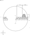
- FIG. FIG. 8 is a partially enlarged cross-sectional view showing a conventional semiconductor device for comparison, and corresponds to FIG. 9 is a partially enlarged plan view of the semiconductor device shown in FIG. 8, corresponding to FIG. 3.
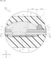
- FIG. 10 is an example of a flowchart showing a method of manufacturing the semiconductor device shown in FIG. 11A and 11B are partially enlarged cross-sectional views showing the steps involved in the method of manufacturing the semiconductor device of FIG. 12A and 12B are partially enlarged cross-sectional views showing steps in the method of manufacturing the semiconductor device of FIG. 13A and 13B are partially enlarged cross-sectional views showing the steps involved in the method of manufacturing the semiconductor device of FIG. 14A and 14B are partially enlarged cross-sectional views showing the steps involved in the method of manufacturing the semiconductor device of FIG.
- FIG. 15 is a partially enlarged cross-sectional view showing a semiconductor device according to a second embodiment of the present disclosure; FIG.
- FIG. 16 is a partially enlarged cross-sectional view showing a semiconductor device according to a third embodiment of the present disclosure
- FIG. 17 is a partially enlarged cross-sectional view showing a semiconductor device according to a fourth embodiment of the present disclosure
- FIG. 18 is a partially enlarged cross-sectional view showing a semiconductor device according to a fifth embodiment of the present disclosure
- FIG. 19 is a partially enlarged cross-sectional view showing a semiconductor device according to a sixth embodiment of the present disclosure
- FIG. 20 is a partially enlarged plan view showing a semiconductor device according to a seventh embodiment of the present disclosure
- FIG. 1 A semiconductor device A10 according to the first embodiment of the present disclosure will be described based on FIGS. 1 to 7.
- FIG. The semiconductor device A10 includes a light emitting element 11, a light receiving element 12, a conductive support member 2, a plurality of wires 4, a transparent resin 5, white resins 61 and 62, and a sealing resin 7.
- FIG. 1 is a plan view showing the semiconductor device A10.
- FIG. 2 is a plan view of the semiconductor device A10.
- the transparent resin 5, the white resins 61 and 62, and the sealing resin 7 are transparent, and the outlines of the respective resins are indicated by imaginary lines (double-dot chain lines).
- 3 is a partially enlarged view of FIG. 2.
- FIG. 4 is a front view of the semiconductor device A10.
- FIG. 5 is a right side view of the semiconductor device A10.
- FIG. 6 is a cross-sectional view taken along line VI-VI of FIG. 7 is a partially enlarged view of FIG. 6.
- the semiconductor device A10 shown in these figures is a device that is surface-mounted on circuit boards of various devices.
- the application and function of the semiconductor device A10 are not limited.
- the package format of the semiconductor device A10 is SOP (Small Outline Package). Note that the package format of the semiconductor device A10 is not limited to the SOP.
- a portion of the semiconductor device A10 covered with the sealing resin 7 has a rectangular shape when viewed in the thickness direction (planar view).
- the thickness direction of the semiconductor device A10 is defined as the z-direction, and the extending direction of the terminals of the semiconductor device A10 (the terminal portions 212 of the leads 21 to be described later, etc.) perpendicular to the z-direction (vertical direction in FIGS. 1 to 3).
- Each dimension of the semiconductor device A10 is not particularly limited.
- the conductive support member 2 is a conductive member that constitutes a conductive path between the light emitting element 11, the light receiving element 12, and the circuit board on which the semiconductor device A10 is mounted.
- the conductive support member 2 is part of a lead frame used when manufacturing the semiconductor device A10. Although the thickness of the conductive support member 2 is not particularly limited, it is, for example, about 200 ⁇ m.
- the conductive support member 2 is preferably made of either Cu or Ni, an alloy thereof, 42 alloy, or the like.
- the conductive support member 2 includes leads 21-28. Each lead 21-28 is spaced apart from each other.
- the lead 21 supports the light emitting element 11 and is electrically connected with the light emitting element 11 .
- the lead 21 has a first die pad 211 and a terminal portion 212 .
- the first die pad 211 is arranged in the semiconductor device A10 near the y1 side in the y direction and in the center (or approximately the center) in the x direction.
- the light emitting element 11 is mounted on the first die pad 211 .
- the first die pad 211 is covered with the transparent resin 5 , the white resin 61 and the sealing resin 7 .
- the first die pad 211 has a rectangular shape (or a substantially rectangular shape) when viewed in the z direction.
- the first die pad 211 as shown in FIGS. 3 and 7, has a main surface 211a, a back surface 211b, a counter surface 211c, and two side surfaces 211d.
- the main surface 211a and the back surface 211b face opposite sides in the z-direction, as shown in FIGS.
- the main surface 211a faces the z2 side
- the back surface 211b faces the z1 side.
- Each of the main surface 211a and the back surface 211b is flat (or substantially flat).
- the light emitting element 11 is bonded to the main surface 211a.
- the opposing surface 211c is connected to the main surface 211a and the back surface 211b and faces the y direction y2.
- the opposing surface 211c as shown in FIGS. 3 and 7, faces the opposing surface 221c of the second die pad 221, which will be described later.
- the two side surfaces 211d are connected to the main surface 211a, the back surface 211b, and the opposing surface 211c, respectively, as shown in FIG.
- One side face 211d faces the x direction x1 side
- the other side face 211d faces the x direction x2 side.
- the terminal portion 212 is connected to the first die pad 211 on the y-direction y1 side, extends in the y-direction y1 side, and is partly exposed from the sealing resin 7 .
- the terminal portion 212 is electrically connected to the light emitting element 11 via the first die pad 211 .
- a portion of the terminal portion 212 covered with the sealing resin 7 is provided with a through hole penetrating in the z direction. The through holes are provided to improve adhesion between the leads 21 and the sealing resin 7 .
- the portion of the terminal portion 212 exposed from the sealing resin 7 is bent like a hook when viewed in the x direction. Note that the shape of the lead 21 is not limited to the above.
- the lead 23 is electrically connected to the light emitting element 11.
- the lead 23 has a pad portion 231 and a terminal portion 232 .
- the pad section 231 is arranged on the x-direction x2 side of the first die pad 211, as shown in FIG.
- the pad portion 231 is electrically connected to the light emitting element 11 via a wire 4 (a wire 41 to be described later).
- the pad portion 231 is covered with the white resin 61 and the sealing resin 7 .
- the pad portion 231 has a rectangular shape (or a substantially rectangular shape) when viewed in the z direction.
- the wire 41 is joined to the surface of the pad portion 231 facing the z-direction z2 side.
- the terminal portion 232 is connected to the pad portion 231 on the y-direction y1 side, extends in the y-direction y1 side, and is partly exposed from the sealing resin 7 .
- the terminal portion 232 is electrically connected to the light emitting element 11 via the pad portion 231 and the wire 41 .
- a portion of the terminal portion 232 covered with the sealing resin 7 is provided with a through hole penetrating in the z direction. The through holes are provided to improve adhesion between the leads 23 and the sealing resin 7 .
- a portion of the terminal portion 232 exposed from the sealing resin 7 is bent like a hook when viewed in the x direction. Note that the shape of the lead 23 is not limited to the above.
- the lead 24 is a so-called dummy terminal and is arranged on the x1 side of the lead 21 in the x direction.
- the lead 24 has a terminal portion 242 .
- the terminal portion 242 extends in the y direction y1 and is partly exposed from the sealing resin 7 .
- a portion of the terminal portion 242 covered with the sealing resin 7 is provided with a through hole penetrating in the z direction.
- the through holes are provided to improve adhesion between the leads 24 and the sealing resin 7 .
- a portion of the terminal portion 242 exposed from the sealing resin 7 is bent like a hook when viewed in the x direction. Note that the shape of the lead 24 is not limited to the above.
- the lead 25 is a so-called dummy terminal and is arranged on the x2 side of the lead 23 in the x direction.
- the lead 25 has a terminal portion 252 .
- the terminal portion 252 extends in the y direction y1 and is partly exposed from the sealing resin 7 .
- a portion of the terminal portion 252 covered with the sealing resin 7 is provided with a through hole penetrating in the z direction.
- the through holes are provided to improve adhesion between the leads 25 and the sealing resin 7 .
- the portion of the terminal portion 252 exposed from the sealing resin 7 is bent like a hook when viewed in the x direction. Note that the shape of the lead 25 is not limited to the above.
- the terminal portions 242, 212, 232, and 252 protrude from the surface of the sealing resin 7 on the y-direction y1 side (a resin side surface 75 described later), and extend from the x-direction x1 side to the x2 side in this order. They are arranged at equal intervals.
- the lead 22 supports the light receiving element 12 and is electrically connected to the light receiving element 12 .
- the lead 22 has a second die pad 221 and a terminal portion 222 .
- the second die pad 221 is arranged in the semiconductor device A10 on the y2 side in the y direction and in the center (or approximately the center) in the x direction.
- the second die pad 221 has the light receiving element 12 mounted thereon.
- the second die pad 221 is electrically connected to the light receiving element 12 via a wire 4 (a wire 43 to be described later).
- the second die pad 221 is covered with a transparent resin 5 and white resins 61 and 62 .
- the second die pad 221 has a rectangular shape (or a substantially rectangular shape) when viewed in the z direction.
- the second die pad 221, as shown in FIGS. 3 and 7, has a main surface 221a, a back surface 221b, a counter surface 221c, and two side surfaces 221d.
- the main surface 221a and the back surface 221b face opposite sides in the z-direction, as shown in FIGS.
- the main surface 221a faces the z2 side
- the back surface 221b faces the z1 side.
- Each of the main surface 211a and the back surface 211b is flat (or substantially flat).
- the light receiving element 12 is bonded to the main surface 221a.
- the opposing surface 221c is connected to the main surface 221a and the back surface 221b and faces the y direction y1.
- the opposing surface 221c faces the opposing surface 211c of the first die pad 211, as shown in FIGS.
- the two side surfaces 221d are connected to the main surface 221a, the back surface 221b, and the opposing surface 221c, respectively, as shown in FIG.
- One side surface 221d faces the x direction x1 side
- the other side surface 221d faces the x direction x2 side.
- the terminal portion 222 is connected to the x-direction x2 side of the second die pad 221, extends in the y-direction y2 side, and is partly exposed from the sealing resin 7. As shown in FIG. The terminal portion 222 is electrically connected to the light receiving element 12 via the second die pad 221 and the wire 43 . A portion of the terminal portion 222 covered with the sealing resin 7 is provided with a through hole penetrating in the z direction. The through holes are provided to improve adhesion between the leads 22 and the sealing resin 7 . As shown in FIG. 5, the portion of the terminal portion 222 exposed from the sealing resin 7 is bent like a hook when viewed in the x direction. Note that the shape of the lead 22 is not limited to the above.
- the lead 26 is electrically connected to the light receiving element 12 .
- the lead 26 has a pad portion 261 and a terminal portion 262 .
- the pad section 261 is arranged on the x-direction x1 side of the second die pad 221, as shown in FIG.
- the pad portion 261 is electrically connected to the light receiving element 12 via a wire 4 (a wire 42 to be described later).
- the pad portion 261 is covered with the white resin 61 and the sealing resin 7 .
- the pad portion 261 has a rectangular shape (or a substantially rectangular shape) when viewed in the z direction.
- the wire 42 is joined to the surface of the pad portion 261 facing the z-direction z2 side.
- the terminal portion 262 is connected to the pad portion 261 on the y-direction y2 side, extends in the y-direction y2 side, and is partly exposed from the sealing resin 7 .
- the terminal portion 262 is electrically connected to the light receiving element 12 via the pad portion 261 and the wire 42 .
- a portion of the terminal portion 262 covered with the sealing resin 7 is provided with a through hole penetrating in the z direction. The through holes are provided to improve adhesion between the leads 26 and the sealing resin 7 .
- a portion of the terminal portion 262 exposed from the sealing resin 7 is bent like a hook when viewed in the x direction. Note that the shape of the lead 26 is not limited to the above.
- the lead 27 is electrically connected to the light receiving element 12 .
- the lead 27 has a pad portion 271 and a terminal portion 272 .
- the pad section 271 is arranged on the y2 side of the second die pad 221 in the y direction, as shown in FIG.
- the pad portion 271 is electrically connected to the light receiving element 12 via a wire 4 (a wire 44 to be described later).
- the pad portion 271 is covered with the sealing resin 7 .
- the pad portion 271 has a rectangular shape (or a substantially rectangular shape) when viewed in the z direction.
- the wire 44 is joined to the surface of the pad portion 271 facing the z-direction z2 side.
- the terminal portion 272 is connected to the pad portion 271 on the y-direction y2 side, extends in the y-direction y2 side, and is partly exposed from the sealing resin 7 .
- the terminal portion 272 is electrically connected to the light receiving element 12 via the pad portion 271 and the wire 44 .
- a portion of the terminal portion 272 covered with the sealing resin 7 is provided with a through hole penetrating in the z direction. The through holes are provided to improve adhesion between the leads 27 and the sealing resin 7 .
- a portion of the terminal portion 272 exposed from the sealing resin 7 is bent like a hook when viewed in the x direction. Note that the shape of the lead 27 is not limited to the above.
- the lead 28 is electrically connected to the light receiving element 12.
- the lead 28 has a pad portion 281 and a terminal portion 282 .
- the pad section 281 is arranged on the y-direction y2 side of the second die pad 221 and on the x-direction x2 side of the pad section 271, as shown in FIG.
- the pad portion 281 is electrically connected to the light receiving element 12 via a wire 4 (a wire 45 to be described later).
- the pad portion 281 is covered with the sealing resin 7 .
- the pad portion 281 has a rectangular shape (or a substantially rectangular shape) when viewed in the z direction.
- the wire 45 is joined to the surface of the pad portion 281 facing the z-direction z2 side.
- the terminal portion 282 is connected to the pad portion 281 on the y-direction y2 side, extends in the y-direction y2 side, and is partly exposed from the sealing resin 7 .
- the terminal portion 282 is electrically connected to the light receiving element 12 via the pad portion 281 and the wire 45 .
- a portion of the terminal portion 282 covered with the sealing resin 7 is provided with a through hole penetrating in the z direction. The through holes are provided to improve adhesion between the leads 28 and the sealing resin 7 .
- a portion of the terminal portion 282 exposed from the sealing resin 7 is bent like a hook when viewed in the x direction. Note that the shape of the lead 28 is not limited to the above.
- the terminal portions 262, 272, 282, and 222 protrude from the surface of the sealing resin 7 on the y-direction y2 side (a resin side surface 76 described later), and extend from the x-direction x1 side to the x2 side in this order. They are arranged at equal intervals.
- the portions of the leads 21 to 28 exposed from the sealing resin 7 may be plated with an alloy containing Sn as a main component, for example.
- the region of the main surface 211a of the first die pad 211 to which the light emitting element 11 is bonded, the region of the main surface 221a of the second die pad 221 to which the light receiving element 12 or the wire 43 is bonded, and the pad portions 231, 261, 271 , 281 may be formed with a plating layer of Ag, for example.
- the light emitting element 11 is, for example, an LED chip, and is configured to emit light of a certain wavelength.
- a constituent material of the light emitting element 11 includes a semiconductor material.
- the light emitting element 11 has a rectangular plate shape when viewed in the z direction.
- the light emitting element 11 has a main surface 111 and a back surface 112 as shown in FIG.
- the main surface 111 and the back surface 112 face opposite sides in the z-direction.
- the main surface 111 faces the z-direction z2 side.
- the back surface 112 faces the z-direction z1 side.
- the light emitting element 11 includes a cathode electrode (not shown) arranged on the main surface 111 and an anode electrode (not shown) arranged on the back surface 112 .
- the light emitting element 11 is bonded to the main surface 211a of the first die pad 211 via a bonding material (not shown).
- the bonding material is a conductive bonding material, and is not particularly limited, but is, for example, solder.
- the back surface 112 of the light emitting element 11 is bonded to the main surface 211a of the first die pad 211 with a bonding material.
- An anode electrode of the light emitting element 11 is conductively connected to the first die pad 211 via a bonding material.
- the terminal portion 212 of the lead 21 is electrically connected to the anode electrode of the light emitting element 11 and functions as an anode terminal.
- the cathode electrode of the light emitting element 11 is conductively connected to the pad portion 231 of the lead 23 via the wire 41, as shown in FIG. As a result, the terminal portion 232 of the lead 23 is electrically connected to the cathode electrode of the light emitting element 11 and functions as a cathode terminal.
- the light emitting element 11 is entirely covered with a transparent resin 5 .
- the light emitting element 11 emits light according to the current that flows when a voltage is applied between the anode electrode and the cathode electrode.
- the light emitted by the light emitting element 11 travels through the transparent resin 5 . Since the entire light emitting element 11 is covered with the transparent resin 5 , the light emitted by the light emitting element 11 is efficiently sent to the light receiving element 12 .
- the light receiving element 12 receives light emitted by the light emitting element 11 .
- a constituent material of the light receiving element 12 includes a semiconductor material.
- the light receiving element 12 has a rectangular plate shape when viewed in the z direction.
- the light receiving element 12 has a main surface 121 and a back surface 122, as shown in FIG.
- the main surface 121 and the back surface 122 face opposite sides in the z-direction.
- the main surface 121 faces the z-direction z2 side.
- the back surface 122 faces the z-direction z1 side.
- the light receiving element 12 is bonded to the main surface 221a of the second die pad 221 via a bonding material (not shown), as shown in FIG.
- the bonding material is not particularly limited, but is, for example, an insulating bonding material.
- the back surface 122 of the light receiving element 12 is bonded to the main surface 221a of the second die pad 221 with a bonding material.
- the light emitting element 11 and the light receiving element 12 are arranged in the y direction.
- a light receiving portion 121a and a circuit forming portion 121b are arranged on the main surface 121 of the light receiving element 12, as shown in FIGS.
- the light receiving portion 121a is arranged on the main surface 121 closer to the y1 side in the y direction.
- the light receiving section 121a has, for example, a photodiode, and generates an electromotive force according to the amount of received light.
- a region of the main surface 121 of the light receiving element 12 where the light receiving portion 121 a is arranged is entirely covered with the transparent resin 5 . Thereby, the light receiving portion 121 a can appropriately receive the light from the light emitting element 11 through the transparent resin 5 .
- the circuit forming portion 121b is arranged on the y2 side from the center of the main surface 121 in the y direction.
- a circuit including a transistor or the like is formed in the circuit forming portion 121b.
- the circuit forming portion 121b amplifies and outputs an electromotive force generated by the light receiving portion 121a upon receiving light.
- a plurality of electrodes are arranged in the circuit forming portion 121b. Each electrode is conductively connected to leads 22, 26, 27 and 28 via wires 4, as shown in FIG. Specifically, the power electrode of the light receiving element 12 is conductively connected to the pad portion 261 of the lead 26 via the wire 42 .
- the terminal portion 262 of the lead 26 is electrically connected to the power supply electrode of the light receiving element 12 and functions as a power supply terminal.
- a ground electrode of the light receiving element 12 is conductively connected to the second die pad 221 via the wire 43 .
- the terminal portion 222 of the lead 22 is electrically connected to the ground electrode of the light receiving element 12 and functions as a ground terminal.
- the output electrode of the light receiving element 12 is conductively connected to the pad portion 271 of the lead 27 via the wire 44 .
- the terminal portion 272 of the lead 27 is electrically connected to the output electrode of the light receiving element 12 and functions as an output terminal.
- the light-receiving element 12 has a low-voltage malfunction prevention function that stops outputting when the power supply voltage drops.
- the light receiving element 12 has a detection electrode that outputs a low voltage detection signal indicating that the power supply voltage has dropped.
- the detection electrode is conductively connected to the pad portion 281 of the lead 28 via the wire 45 .
- the terminal portion 282 of the lead 28 is electrically connected to the detection electrode of the light receiving element 12 and functions as a detection terminal.
- a region of the main surface 121 of the light receiving element 12 where the circuit forming portion 121b is arranged is exposed from the transparent resin 5 and is entirely covered with the white resin 61 or the white resin 62 . As a result, the light emitted from the light emitting element 11 is not applied to the circuit forming portion 121b.
- the semiconductor device A10 can transmit a signal from the input side to the output side while the input side (the terminal portions 212 and 232) and the output side (the terminal portion 272) are electrically insulated. can be done.
- the plurality of wires 4 are conductive members that form conductive paths between the light-emitting element 11 and the light-receiving element 12 and the circuit board together with the conductive support member 2 .
- a constituent material of each of the plurality of wires 4 is a metal containing Au, Cu, or Al, for example.
- the plurality of wires 4 includes wires 41-45.
- the wire 41 constitutes a conductive path between the light emitting element 11 and the lead 23.
- the wire 41 is joined to the cathode electrode of the light emitting element 11 and the pad portion 231 of the lead 23 .
- the number of wires 41 is not limited.
- the wire 42 constitutes a conductive path between the light receiving element 12 and the lead 26. As shown in FIG. The wire 42 is joined to the power electrode of the light receiving element 12 and the pad portion 261 of the lead 26 . Note that the number of wires 42 is not limited.
- the wire 43 constitutes a conductive path between the light receiving element 12 and the lead 22 . The wire 43 is joined to the ground electrode of the light receiving element 12 and the second die pad 221 . Note that the number of wires 43 is not limited.
- Wire 44 constitutes a conductive path between light receiving element 12 and lead 27 .
- the wire 44 is joined to the output electrode of the light receiving element 12 and the pad portion 271 of the lead 27 .
- the wire 45 constitutes a conductive path between the light receiving element 12 and the lead 28. As shown in FIG.
- the wire 45 is joined to the detection electrode of the light receiving element 12 and the pad portion 281 of the lead 28 . Note that the number of wires 45 is not limited.
- the transparent resin 5 includes a portion of the conductive support member 2, the entire light emitting element 11, a portion of the light receiving element 12 (the portion where the light receiving portion 121a is arranged), It covers part of the wire 41 .
- the transparent resin 5 has electrical insulation.
- Transparent resin 5 contains, for example, a transparent epoxy resin.
- the constituent material of the transparent resin 5 is not limited as long as it is a material having translucency.
- the transparent resin 5 is formed by placing a mold on the z-direction z1 side of the lead frame that becomes the conductive support member 2 and potting the transparent resin 5 material from the z-direction z2 side.
- the transparent resin 5 has a dome shape bulging in the z direction z2.
- the transparent resin 5 includes a portion located on the z-direction z1 side from the back surface 211b and the back surface 221b between the first die pad 211 and the second die pad 221 when viewed in the z-direction.
- the transparent resin 5 partially covers the back surface 211b and the back surface 221b.
- the transparent resin 5 may cover the entire surface of the back surface 211b or the back surface 221b.
- the maximum value of the height (dimension in the z direction) from the conductive support member 2 of the portion of the transparent resin 5 formed on the z-direction z1 side of the conductive support member 2 is the z-direction z2 side of the conductive support member 2. It is sufficiently smaller than the maximum value of the height (dimension in the z direction) from the conductive support member 2 of the portion formed in . That is, the transparent resin 5 is formed thicker on the z-direction z2 side of the conductive support member 2 and thinner on the z1 side. A portion of the transparent resin 5 that is formed on the z-direction z1 side of the conductive support member 2 is formed in a fixed shape because it is formed by a mold.
- the transparent resin 5 has a transparent resin main surface 51 and a transparent resin back surface 52, as shown in FIG.
- the transparent resin main surface 51 and the transparent resin back surface 52 face opposite sides in the z direction.
- the transparent resin main surface 51 faces the z-direction z2 side
- the transparent resin rear surface 52 faces the z-direction z1 side.
- the transparent resin main surface 51 is a dome-shaped curved surface bulging in the z direction z2.
- the transparent resin back surface 52 is the surface of a portion (including a portion covering the back surface 211b and the back surface 221b) located on the z-direction z1 side of the back surface 211b and the back surface 221b. Concavities and convexities are formed on the transparent resin rear surface 52 .
- the shape, arrangement, and unevenness difference of the unevenness are not limited.
- the unevenness is formed by the unevenness formed on the mold.
- the transparent resin main surface 51 is smooth because it is formed by the surface tension of the material of the transparent resin 5 during potting. Therefore, the transparent resin back surface 52 has a larger surface roughness than the transparent resin main surface 51 .
- the transparent resin 5 has an elliptical shape (or a substantially elliptical shape) elongated in the x direction when viewed in the z direction.
- the y-direction dimension W1 of the transparent resin 5 is preferably small, and the x-direction dimension W2 is preferably large.
- Dimension W2 is preferably larger than dimension W1, more preferably 1.5 times or more of dimension W1.
- the transparent resin 5 covers the entire opposing surface 211 c of the first die pad 211 and the opposing surface 221 c of the second die pad 221 . Further, the interface between the transparent resin 5 and the white resin 61 protrudes outward from the two side surfaces 211d of the first die pad 211 when viewed in the z direction.
- the white resins 61 and 62 are electrically insulating and white-colored, for example, silicone resin.
- the constituent material of the white resins 61 and 62 is not limited.
- the white resin 61 covers the entire transparent resin 5 .
- the light emitted by the light emitting element 11 is reflected at the interface between the transparent resin 5 and the white resin 61 and travels inside the transparent resin 5 .
- the white resin 61 has an elliptical shape (or a substantially elliptical shape) elongated in the x direction when viewed in the z direction.
- a larger dimension W4 of the white resin 61 in the x direction is desirable.
- the dimension W4 is preferably larger than the dimension W3 in the y direction, more preferably 1.5 times or more of the dimension W3.
- the white resin 61 covers the entire surface of each of the two side surfaces 221d of the second die pad 221. As shown in FIG.
- the white resin 61 is formed by potting the material of the white resin 61 so as to cover the entire transparent resin 5 .
- the surface of the white resin 61 is smooth because it is formed by the surface tension of the material of the white resin 61 during potting.
- the white resin 62 is in contact with the main surface 121 of the light receiving element 12, and is arranged at the center (or approximately the center) of the main surface 121 in the y direction so as to cover the entire area in the x direction.
- the white resin 62 is formed on the circuit forming portion 121b so as not to cover the light receiving portion 121a. Also, the white resin 62 is in contact with both the transparent resin 5 and the white resin 61 .
- the white resin 62 is formed by potting the material of the white resin 62 .
- the white resin 62 is formed before the transparent resin 5 is formed, and dams up the material flow of the fluidized transparent resin 5 during the formation of the transparent resin 5 .
- the transparent resin 5 is formed so as to cover the light receiving portion 121a and not cover the circuit forming portion 121b.
- the constituent materials of the white resin 61 and the white resin 62 are desirably the same material, but they do not necessarily have to be the same.
- the white resins 61 and 62 resins of colors other than white may be used.
- the color of the resin is not limited as long as the resin can reflect the light emitted by the light emitting element 11 at the interface with the transparent resin 5 . However, in order to reflect light efficiently, it is desirable to be white.
- the sealing resin 7 partially covers the conductive support member 2 and the entire light emitting element 11 , light receiving element 12 , wires 4 , transparent resin 5 , and white resins 61 and 62 .
- the sealing resin 7 has electrical insulation.
- Sealing resin 7 contains, for example, black epoxy resin.
- the constituent material of the sealing resin 7 is not limited.
- the sealing resin 7 is formed, for example, by transfer molding using a mold.
- the sealing resin 7 has a rectangular shape when viewed in the z direction.
- the sealing resin 7 has a resin top surface 71, a resin bottom surface 72, and resin side surfaces 73-76.
- the resin top surface 71 and the resin bottom surface 72 face opposite sides in the z-direction.
- the resin top surface 71 faces the z-direction z2 side, and the resin bottom surface 72 faces the z-direction z1 side.
- the resin top surface 71 and the resin bottom surface 72 are flat (or substantially flat).
- Each of the resin side surfaces 73 to 76 is connected to the resin top surface 71 and the resin bottom surface 72, and is sandwiched between the resin top surface 71 and the resin bottom surface 72 in the z-direction.
- the resin side surface 73 and the resin side surface 74 face opposite sides in the x direction.
- the resin side surface 73 faces the x1 side in the x direction, and the resin side surface 74 faces the x2 side in the x direction.
- the resin side surface 75 and the resin side surface 76 face opposite sides in the y direction.
- the resin side surface 75 faces the y1 side in the y direction, and the resin side surface 76 faces the y2 side in the y direction. As shown in FIG.
- each of the terminal portions 242 , 212 , 232 and 252 protrudes from the resin side surface 75 .
- a part of each of the terminal portions 262 , 272 , 282 , 222 protrudes from the resin side surface 76 .
- the conductive support member 2 is not exposed from the resin side surface 73 and the resin side surface 74 .
- the resin side surfaces 73 to 76 each have surfaces connected to the resin top surface 71 and inclined so as to approach each other toward the resin top surface 71 . That is, the portion of the sealing resin 7 connected to the resin top surface 71 and surrounded by the inclined surfaces has a tapered shape in which the cross-sectional area in the xy plane becomes smaller toward the resin top surface 71 . Further, the resin side surfaces 73 to 76 each have surfaces connected to the resin bottom surface 72 and inclined so as to approach each other toward the resin bottom surface 72 .
- the portion of the sealing resin 7 connected to the resin bottom surface 72 and surrounded by the inclined surfaces has a tapered shape in which the cross-sectional area in the xy plane becomes smaller toward the resin bottom surface 72 .
- the shape of the sealing resin 7 shown in FIGS. 1, 4, and 5 is an example.
- the shape of the sealing resin 7 is not limited to the illustrated shape.
- FIG. 10 An example of a method for manufacturing the semiconductor device A10 will be described below with reference to FIGS. 10 to 14.
- FIG. 10
- FIG. 10 is an example of a flowchart showing a method of manufacturing the semiconductor device A10.
- 11 to 14 are partially enlarged cross-sectional views showing steps related to the method of manufacturing the semiconductor device A10, and correspond to FIG. Note that the x-direction, y-direction, and z-direction shown in FIGS. 11 to 14 are the same directions as in FIGS.
- the method of manufacturing the semiconductor device A10 includes a lead frame forming step S10, a die bonding step S20, a wire bonding step S30, a damming resin forming step S40, a transparent resin forming step S50, a white resin forming step S60, a A stopper resin forming step S70 and a cutting step S80 are provided.
- the lead frame forming step S10 is a step of forming a lead frame from a metal plate.
- a metal plate is prepared as a material for the lead frame.
- the lead frame 91 is formed by punching or etching the metal plate.
- the lead frame 91 has a main surface 911 and a back surface 912 facing opposite to each other in the z-direction (see FIG. 11).
- the die bonding step S20 is a step of bonding the light emitting element 11 and the light receiving element 12 to the lead frame 91.
- the light-emitting element 11 is bonded via a bonding material to the portion of the main surface 911 of the lead frame 91 that will become the first die pad 211 (see FIG. 11).
- the light receiving element 12 is bonded to the portion of the main surface 911 of the lead frame 91 that will become the second die pad 221 via a bonding material (see FIG. 11).
- the bonding method of the light emitting element 11 and the light receiving element 12 in the die bonding step S20 is not limited.
- the wire bonding step S30 is a step of forming the wires 4.
- the wire 41 is joined to the cathode electrode of the light emitting element 11 and the portion of the main surface 911 of the lead frame 91 that will become the pad portion 231 .
- Wires 42 to 45 are joined to the respective electrodes of the light receiving element 12 and predetermined positions on the main surface 911 of the lead frame 91, respectively. Note that the method of forming the wires 4 in the wire bonding step S30 is not limited.
- the damming resin forming step S40 is a step of forming the white resin 62.
- the white resin 62 is formed by potting the material of the white resin 62 on the main surface 121 of the light receiving element 12 bonded to the main surface 911 of the lead frame 91 and curing the material. do.
- the white resin 62 is formed so as not to cover the light receiving portion 121 a of the light receiving element 12 .
- the transparent resin forming step S50 is a step of forming the transparent resin 5.
- the lead frame 91 is placed on the mounting surface 921 of the mold 92 with the rear surface 912 facing downward.
- the mold 92 has a recess 922 that is recessed from the mounting surface 921 in the z direction z1.
- the concave portion 922 includes a portion located between the light emitting element 11 and the light receiving element 12 when viewed in the z direction. Concave and convex portions are formed in the concave portion 922 .
- the transparent resin 5 is formed by potting the material of the transparent resin 5 from the main surface 911 side (z direction z2 side) of the lead frame 91 and hardening it.
- the material of the transparent resin 5 is potted so as to cover the entire light emitting element 11 and part of the light receiving element 12 . At this time, the flow of the material of the transparent resin 5 is blocked by the white resin 62, so that the transparent resin 5 is formed so as to cover the light receiving portion 121a and not cover the circuit forming portion 121b.
- the transparent resin rear surface 52 of the transparent resin 5 has a shape defined by the concave portion 922 of the mold 92 . Therefore, unevenness is formed on the transparent resin rear surface 52 .
- the transparent resin main surface 51 of the transparent resin 5 becomes a dome-shaped smooth curved surface bulging in the z-direction z2 side due to the surface tension of the material of the transparent resin 5 during potting. The viscosity and dropping amount of the material of the transparent resin 5 are adjusted so that the shape of the transparent resin main surface 51 becomes a desired shape.
- the white resin forming step S60 is a step of forming the white resin 61.
- the white resin 61 is formed by potting the material of the white resin 61, covering the entire transparent resin 5, and hardening it.
- the surface of the white resin 61 becomes a smooth curved surface due to the surface tension of the material of the white resin 61 during potting.
- the viscosity and dropping amount of the material of the white resin 61 are adjusted so that the white resin 61 has a desired shape.
- the encapsulation resin forming step S70 is a step of forming the encapsulation resin 7 .
- this step by curing the material of the sealing resin 7, a part of the lead frame 91, the light emitting element 11, the light receiving element 12, the wires 4, the transparent resin 5, and the white resins 61 and 62 are entirely removed.
- a covering sealing resin 7 is formed.
- the process is performed, for example, by well-known transfer molding using a mold. Specifically, the lead frame 91 with the white resin 61 formed thereon is set in a molding machine. Next, the material of the fluidized white resin 61 is poured into the cavity in the mold, molded, and cured. As described above, the sealing resin 7 is formed.
- the method of forming the sealing resin 7 in the sealing resin forming step S70 is not limited.
- the cutting step S80 is a step of cutting the lead frame 91 .
- a blade is used to cut the lead frame 91 into individual pieces.
- an individual piece to be the semiconductor device A10 is formed.
- the cutting method in the cutting step S80 is not limited.
- portions of the terminal portions 212, 222, 232, 242, 252, 262, 272, and 282 protruding from the sealing resin 7 are bent. Through the above steps, the semiconductor device A10 described above is manufactured.
- the interface between the transparent resin back surface 52 and the white resin 61 between the first die pad 211 and the second die pad 221 (hereinafter referred to as the "back surface side interface") ) has a large interfacial distance.
- the dielectric breakdown voltage of the semiconductor device A10 is improved.
- the transparent resin 5 includes a portion located on the z-direction z1 side from the back surface 211b and the back surface 221b between the first die pad 211 and the second die pad 221 when viewed in the z-direction.
- the dielectric strength of the semiconductor device A10 is further improved.
- the transparent resin 5 partially covers the back surface 211b and the back surface 221b. Therefore, compared with the case where the transparent resin back surface 52 does not cover the back surface 211b and the back surface 221b, the interfacial distance of the back surface side interface is large. As a result, the dielectric strength of the semiconductor device A10 is further improved.
- FIG. 8 and 9 are diagrams showing a conventional semiconductor device A100 for comparison.
- FIG. 8 is a partially enlarged cross-sectional view of the semiconductor device A100, corresponding to FIG.
- FIG. 9 is a partially enlarged plan view of the semiconductor device A100, corresponding to FIG.
- the semiconductor device A100 differs from the semiconductor device A10 in the shape of the transparent resin 5 .
- the transparent resin back surface 52 is flush with the back surfaces 211b and 221b. Since the back surface side interface (see thick line arrow d5' in FIG. 8) is linearly arranged, the interface distance of the back surface side interface is short.
- the interface distance on the back side interface is the same as in the case of the semiconductor device A100 (see the thick line arrow d5′ in FIG. 8). ), it is larger. As a result, the dielectric breakdown voltage of the semiconductor device A10 is improved.
- the transparent resin 5 has an elliptical shape (or a substantially elliptical shape) elongated in the x direction when viewed in the z direction. Therefore, compared to the case where the transparent resin 5 has a circular shape when viewed in the z direction or an elliptical shape (or a substantially elliptical shape) elongated in the y direction, the transparent resin 5 between the first die pad 211 and the second die pad 221 is Of the interfaces with the white resin 61, interfaces on both ends in the x direction (hereinafter referred to as "side interfaces”) have a large interface distance.
- the transparent resin 5 covers the entire surfaces of the facing surface 211c of the first die pad 211 and the facing surface 221c of the second die pad 221, respectively. Therefore, each side interface is connected to the side surface 211d of the first die pad 211 and the side surface 221d of the second die pad 221 (see thick line arrows d1 and d2 in FIG. 3).
- the facing surface 211c of the first die pad 211 and the facing surface 221c of the second die pad 221 have portions not covered with the transparent resin 5, as shown in FIG. In FIG. 9 , the side interface (see thick arrow d1′ in FIG.
- the transparent resin 5 covers the entire facing surface 211c and the facing surface 221c, respectively, so that the interface distance of each side interface (see thick line arrows d1 and d2 in FIG. 3) is equal to that of the semiconductor device A10.
- A100 see thick line arrows d1' and d2' in FIG. 9
- the dielectric breakdown voltage of the semiconductor device A10 is improved.
- the white resin 61 has an elliptical shape (or a substantially elliptical shape) elongated in the x direction when viewed in the z direction. Therefore, compared to the case where the white resin 61 has a circular shape when viewed in the z-direction or an elliptical shape (or a substantially elliptical shape) elongated in the y-direction, the conductive support member 2 on the input side (the first die pad 211 and the pad portion of the lead 23) 231) and the conductive support member 2 (the second die pad 221 and the pad portion 261 of the lead 26) on the output side. The interfacial distance is large. Comparing FIG. 3 and FIG.
- the semiconductor device A10 has an interface distance between the white resin 61 and the sealing resin 7 on the x-direction x1 side (see the thick arrow d3 in FIG. 3). Compared to the case of the device A100 (see thick line arrow d3' in FIG. 9), it is larger.
- the interface distance of the interface on the x-direction x2 side of the interface between the white resin 61 and the sealing resin 7 is the semiconductor device A100 ( d4'), it is large. As a result, the dielectric breakdown voltage of the semiconductor device A10 is improved.
- the light receiving element 12 has the light receiving portion 121 a covered with the transparent resin 5 and the circuit forming portion 121 b covered with the white resin 61 or the white resin 62 . Therefore, the light receiving portion 121 a can appropriately receive the light from the light emitting element 11 through the transparent resin 5 .
- the circuit forming portion 121b is not irradiated with the light emitted by the light emitting element 11 . Therefore, deterioration of the circuit formed in the circuit forming portion 121b due to light is suppressed.
- the white resin 62 is formed so as not to cover the light receiving portion 121a before forming the transparent resin 5, and dams the fluidized material of the transparent resin 5 when the transparent resin 5 is formed.
- the transparent resin 5 is formed so as to cover the light receiving portion 121a and not cover the circuit forming portion 121b.
- the transparent resin 5 is obtained by arranging the mold 92 on the z-direction z1 side of the lead frame 91, and disposing the material of the transparent resin 5 from the main surface 911 side (z-direction z2 side) of the lead frame 91. Formed by potting.
- the transparent resin 5 is formed by potting without using the mold 92, it is difficult to adjust the transparent resin 5 into a desired shape.
- the portion of the lead frame 91 on the back surface 912 side becomes a smooth curved surface due to the surface tension of the material.
- the shape of the transparent resin rear surface 52 of the transparent resin 5 is defined by the concave portion 922 and formed into a desired shape.
- each of the terminal portions 242 , 212 , 232 , 252 is exposed from the resin side surface 75 .
- a portion of each of the terminal portions 262 , 272 , 282 , 222 is exposed from the resin side surface 76 .
- the conductive support member 2 is not exposed from the resin top surface 71 , the resin bottom surface 72 , the resin side surfaces 73 and the resin side surfaces 74 . That is, there is no metal portion of the conductive support member 2 exposed from the sealing resin 7 between the input-side terminal and the output-side terminal having a large potential difference.
- the insulation distance between the input side terminal and the output side terminal (the exposed portion of the input side terminal from the sealing resin 7 and the exposed portion of the output side terminal from the sealing resin 7 is equal to the sealing resin 7 creepage distance, which is the distance along the surface of the
- the semiconductor device A10 has improved withstand voltage compared to the case where the conductive support member 2 such as the support lead is exposed from the resin side surface 73 or the resin side surface 74 .
- the present invention is not limited to this.
- the transparent resin 5 may be covered with the sealing resin 7 without the white resin 61 provided. Also, the white resin 62 may not be provided.
- FIG. 15 is a diagram for explaining the semiconductor device A20 according to the second embodiment of the present disclosure.
- FIG. 15 is a partially enlarged cross-sectional view showing the semiconductor device A20, corresponding to FIG.
- the semiconductor device A20 according to this embodiment differs from the semiconductor device A10 according to the first embodiment in that the white resin 62 is not provided.
- the configuration and operation of other portions of this embodiment are the same as those of the first embodiment.
- each part of said 1st Embodiment may be combined arbitrarily.
- the semiconductor device A20 does not include the white resin 62.
- the semiconductor device A20 is formed so that the transparent resin 5 does not cover the circuit forming portion 121b of the light receiving element 12 by adjusting the viscosity of the material of the transparent resin 5 and the dropping amount.
- the transparent resin 5 includes a portion located on the z-direction z1 side from the back surface 211b and the back surface 221b between the first die pad 211 and the second die pad 221 when viewed in the z-direction. Moreover, the transparent resin 5 partially covers the back surface 211b and the back surface 221b. Compared with the semiconductor device A100, the semiconductor device A20 has a larger interface distance on the back surface side interface, and thus has an improved withstand voltage.
- the transparent resin 5 is formed by placing the mold 92 on the z-direction z1 side of the lead frame 91 and potting the material of the transparent resin 5 from the main surface 911 side of the lead frame 91 . be. Therefore, the shape of the transparent resin rear surface 52 of the transparent resin 5 is defined by the concave portion 922 and formed into a desired shape. Moreover, the semiconductor device A20 has the same effect as the semiconductor device A10 due to the configuration common to the semiconductor device A10.
- FIG. 16 is a diagram for explaining the semiconductor device A30 according to the third embodiment of the present disclosure.
- FIG. 16 is a partially enlarged cross-sectional view showing the semiconductor device A30, corresponding to FIG.
- the semiconductor device A30 according to this embodiment differs from the semiconductor device A10 according to the first embodiment in that the white resin 61 is not provided.
- the configuration and operation of other portions of this embodiment are the same as those of the first embodiment. Note that each part of the above first and second embodiments may be combined arbitrarily.
- the semiconductor device A30 does not include the white resin 61.
- the semiconductor device A30 does not cover the transparent resin 5 with the white resin 61 but covers it with the sealing resin 7 .
- Light emitted by the light emitting element 11 is reflected at the interface between the transparent resin 5 and the sealing resin 7 and received by the light receiving element 12 .
- the semiconductor device A30 does not have to include the white resin 62, like the semiconductor device A20.
- the transparent resin 5 includes a portion located on the z-direction z1 side from the back surface 211b and the back surface 221b between the first die pad 211 and the second die pad 221 when viewed in the z-direction. Moreover, the transparent resin 5 partially covers the back surface 211b and the back surface 221b. As compared with the semiconductor device A100, the semiconductor device A30 has a larger interface distance on the back surface side interface, and thus has an improved withstand voltage.
- the transparent resin 5 is formed by placing the mold 92 on the z-direction z1 side of the lead frame 91 and potting the material of the transparent resin 5 from the main surface 911 side of the lead frame 91 . be. Therefore, the shape of the transparent resin rear surface 52 of the transparent resin 5 is defined by the concave portion 922 and formed into a desired shape. Further, the semiconductor device A30 has the same effect as the semiconductor device A10 due to the configuration common to the semiconductor device A10.
- FIG. 17 is a diagram for explaining a semiconductor device A40 according to the fourth embodiment of the present disclosure.
- FIG. 17 is a partially enlarged cross-sectional view showing the semiconductor device A40, corresponding to FIG.
- the semiconductor device A40 according to this embodiment differs from the semiconductor device A10 according to the first embodiment in that the transparent resin rear surface 52 is not formed with unevenness.
- the configuration and operation of other portions of this embodiment are the same as those of the first embodiment. Note that each part of the above first to third embodiments may be combined arbitrarily.
- the transparent resin 5 according to this embodiment does not have unevenness formed on the back surface 52 of the transparent resin.
- the transparent resin 5 is formed using a mold 92 in which recesses 922 are not uneven.
- the transparent resin 5 includes a portion located on the z-direction z1 side of the back surface 211b and the back surface 221b between the first die pad 211 and the second die pad 221 when viewed in the z-direction. Moreover, the transparent resin 5 partially covers the back surface 211b and the back surface 221b. Even if the semiconductor device A40 does not have unevenness formed on the transparent resin back surface 52, compared with the semiconductor device A100, the interface distance of the back surface side interface is larger, so the dielectric strength voltage is improved.
- the transparent resin 5 is formed by placing the mold 92 on the z-direction z1 side of the lead frame 91 and potting the material of the transparent resin 5 from the main surface 911 side of the lead frame 91 . be. Therefore, the shape of the transparent resin rear surface 52 of the transparent resin 5 is defined by the concave portion 922 and formed into a desired shape.
- the semiconductor device A40 has the same effect as the semiconductor device A10 due to the configuration common to the semiconductor device A10.
- FIG. 18 is a diagram for explaining a semiconductor device A50 according to the fifth embodiment of the present disclosure.
- FIG. 18 is a partially enlarged cross-sectional view showing the semiconductor device A50, corresponding to FIG.
- the semiconductor device A50 according to this embodiment differs from the semiconductor device A10 according to the first embodiment in the shape of the transparent resin 5.
- FIG. The configuration and operation of other portions of this embodiment are the same as those of the first embodiment. It should be noted that each part of the above-described first to fourth embodiments may be combined arbitrarily.
- the transparent resin 5 does not include a portion located on the z-direction z1 side of the back surface 211b and the back surface 221b between the first die pad 211 and the second die pad 221 when viewed in the z-direction. Moreover, the transparent resin 5 does not have a portion covering part of the back surface 211b or the back surface 221b.
- the transparent resin 5 is formed using a mold 92 in which no recessed portion 922 is formed and the mounting surface 921 is formed with unevenness.
- the semiconductor device A50 has a larger interface distance on the back side interface, and thus has an improved withstand voltage.
- the transparent resin 5 is formed by placing the mold 92 on the z-direction z1 side of the lead frame 91 and potting the material of the transparent resin 5 from the main surface 911 side of the lead frame 91 . be. Therefore, the shape of the transparent resin rear surface 52 of the transparent resin 5 is defined by the mold 92 and formed into a desired shape.
- the semiconductor device A50 has the same effect as the semiconductor device A10 due to the configuration common to the semiconductor device A10. Further, according to the present embodiment, since the transparent resin 5 is not formed on the back surface 211b and the back surface 221b side of the semiconductor device A50, the dimension of the sealing resin 7 in the z direction can be reduced.
- FIG. 19 is a diagram for explaining a semiconductor device A60 according to the sixth embodiment of the present disclosure.
- FIG. 19 is a partially enlarged cross-sectional view showing the semiconductor device A60, corresponding to FIG.
- the semiconductor device A60 according to this embodiment differs from the semiconductor device A10 according to the first embodiment in the shape of the transparent resin 5. As shown in FIG.
- the configuration and operation of other portions of this embodiment are the same as those of the first embodiment. It should be noted that each part of the above-described first to fifth embodiments may be combined arbitrarily.
- the transparent resin 5 according to this embodiment does not have a portion covering part of the back surface 211b or the back surface 221b. That is, the transparent resin 5 does not cover the rear surface 211b and the rear surface 221b.
- the transparent resin 5 includes a portion located on the z-direction z1 side of the back surface 211b and the back surface 221b between the first die pad 211 and the second die pad 221 when viewed in the z-direction. Concavities and convexities are formed on the transparent resin rear surface 52 . Even if the transparent resin 5 does not cover the rear surface 211b and the rear surface 221b, the semiconductor device A60 has a larger interface distance on the rear surface side than the semiconductor device A100, so that the withstand voltage is improved.
- the transparent resin 5 is formed by placing the mold 92 on the z-direction z1 side of the lead frame 91 and potting the material of the transparent resin 5 from the main surface 911 side of the lead frame 91 . be. Therefore, the shape of the transparent resin rear surface 52 of the transparent resin 5 is defined by the mold 92 and formed into a desired shape.
- the semiconductor device A60 has the same effect as the semiconductor device A10 due to the configuration common to the semiconductor device A10.
- the semiconductor devices A10, A40, A50, A60 can freely adjust the shape of the transparent resin back surface 52 by designing the mold 92.
- FIG. 20 is a diagram for explaining a semiconductor device A70 according to the seventh embodiment of the present disclosure.
- FIG. 20 is a partially enlarged plan view showing the semiconductor device A70, corresponding to FIG. In FIG. 20, for convenience of understanding, the transparent resin 5, the white resins 61 and 62, and the sealing resin 7 are shown through, and their external shapes are indicated by imaginary lines (double-dot chain lines).
- the semiconductor device A70 according to this embodiment differs from the semiconductor device A10 according to the first embodiment in the shape of the transparent resin 5 .
- the configuration and operation of other portions of this embodiment are the same as those of the first embodiment. Note that each part of the above first to sixth embodiments may be combined arbitrarily.
- the opposing surface 211c of the first die pad 211 is not entirely covered with the transparent resin 5, but is partially covered with the white resin 61.
- the opposing surface 221 c of the second die pad 221 is not entirely covered with the transparent resin 5 but partially covered with the white resin 61 . That is, the transparent resin 5 only partially covers each of the facing surface 211c and the facing surface 221c.
- the side interface on the x-direction x1 side is connected to the opposing surface 211c of the first die pad 211 and the side surface 221d of the second die pad 221 (see thick arrow d1 in FIG. 20).
- the side interface on the x-direction x2 side is connected to the side surface 211d of the first die pad 211 and the opposing surface 221c of the second die pad 221 (see thick arrow d2 in FIG. 20).
- both side interfaces protrude outward from the two side surfaces 211d of the first die pad 211.
- the transparent resin 5 includes a portion located on the z-direction z1 side from the back surface 211b and the back surface 221b between the first die pad 211 and the second die pad 221 when viewed in the z-direction. Moreover, the transparent resin 5 partially covers the back surface 211b and the back surface 221b. Compared with the semiconductor device A100, the semiconductor device A70 has a larger interface distance on the back surface side interface, so that the withstand voltage is improved.
- the transparent resin 5 does not entirely cover the opposing surface 211c of the first die pad 211 and the opposing surface 221c of the second die pad 221. It protrudes outward from two side surfaces 211 d of 211 . Therefore, the interface distances of the side interfaces (see thick line arrows d1 and d2 in FIG. 20) are larger than those of the semiconductor device A100 (see thick line arrows d1' and d2' in FIG. 9). As a result, the dielectric breakdown voltage of the semiconductor device A70 is improved.
- the transparent resin 5 is formed by placing the mold 92 on the z-direction z1 side of the lead frame 91 and potting the material of the transparent resin 5 from the main surface 911 side of the lead frame 91 . be. Therefore, the shape of the transparent resin rear surface 52 of the transparent resin 5 is defined by the concave portion 922 and formed into a desired shape. Moreover, the semiconductor device A70 has the same effect as the semiconductor device A10 due to the configuration common to the semiconductor device A10.
- the semiconductor device and the semiconductor device manufacturing method according to the present disclosure are not limited to the above-described embodiments.
- the specific configuration of each part of the semiconductor device according to the present disclosure and the specific method of each step of the method for manufacturing the semiconductor device according to the present disclosure can be changed in design in various ways.
- the present disclosure includes embodiments set forth in the following appendices.
- a first lead (21) including a first die pad (211) having a first main surface (211a) and a first back surface (211b) facing opposite to each other in the thickness direction (z direction); A second die pad having a second main surface (221a) facing the same side as the first main surface in the thickness direction, and a second back surface (221b) facing the same side as the first back surface in the thickness direction.
- a second lead (22) comprising (221), a light emitting element (11) mounted on the first main surface; a light receiving element (12) mounted on the second main surface; a transparent resin (5) covering at least part of each of the light emitting element and the light receiving element; a first resin (61) covering the transparent resin; with
- the transparent resin has a transparent resin main surface (51) facing the same side as the first main surface in the thickness direction, and a transparent resin rear surface (52) facing the same side as the first rear surface in the thickness direction. with The semiconductor device, wherein the transparent resin back surface has a surface roughness larger than that of the transparent resin main surface.
- the transparent resin according to appendix 1 wherein the transparent resin includes a portion located on the side facing the first back surface from the first back surface between the first die pad and the second die pad when viewed in the thickness direction. semiconductor equipment.
- Appendix 3. The semiconductor device according to appendix 2, wherein the transparent resin covers at least part of each of the first back surface and the second back surface.
- Appendix 4. ( Figures 3 and 7) 4. The semiconductor device according to any one of appendices 1 to 3, wherein a part of the light receiving element is exposed from the transparent resin. Appendix 5.
- the light receiving element has an element main surface (121) facing the same side as the first main surface,
- the semiconductor device according to appendix 4 wherein the second resin is arranged in contact with the main surface of the element and is in contact with the transparent resin and the first resin.
- Appendix 6. The semiconductor device according to any one of appendices 1 to 5, wherein the first resin is a white resin.
- Appendix 7. (Fig. 3)
- the first die pad has a first opposing surface (211c) facing the second die pad, and two first side surfaces (211d) connected to the first main surface, the first back surface, and the first opposing surface. and 7.
- a lead frame (91) having a main surface (911) and a back surface (912) facing opposite to each other in the thickness direction (S10); a step of bonding a light emitting element (11) and a light receiving element (12) to the lead frame (S20); forming a transparent resin (5) covering at least part of each of the light emitting element and the light receiving element (S50); forming a first resin (61) covering the transparent resin (S60); with
- a mold (92) is arranged on the back surface side of the lead frame, and the material of the transparent resin is potted from the main surface side of the lead frame, A recess (922) including a portion positioned between the light emitting element and the light receiving element when viewed in the thickness direction is formed on the mounting surface (921) of the mold on which the lead frame is mounted.
- a method for manufacturing a semiconductor device Appendix 13. (Fig. 12) 13. The method of manufacturing a semiconductor device according to appendix 12, wherein the concave portion is uneven. Appendix 14. (Fig. 11) Before the step of forming the transparent resin, the step of forming a second resin (62) on the element main surface of the light receiving element facing the same side as the main surface of the lead frame (S40), 14. The method of manufacturing a semiconductor device according to appendix 12 or 13, wherein in the step of forming the transparent resin, the flow of the material of the transparent resin is blocked by the second resin. Appendix 15. After the step of forming the first resin, the step of forming a third resin (7) covering the first resin (S70) is further provided, 15. The method of manufacturing a semiconductor device according to any one of appendices 12 to 14, wherein the first resin is a white resin.
Landscapes
- Structures Or Materials For Encapsulating Or Coating Semiconductor Devices Or Solid State Devices (AREA)
- Engineering & Computer Science (AREA)
- Microelectronics & Electronic Packaging (AREA)
Priority Applications (4)
| Application Number | Priority Date | Filing Date | Title |
|---|---|---|---|
| CN202280058664.6A CN117882201A (zh) | 2021-08-30 | 2022-08-01 | 半导体装置和半导体装置的制造方法 |
| DE112022004213.3T DE112022004213T5 (de) | 2021-08-30 | 2022-08-01 | Halbleitervorrichtung und Verfahren zum Herstellen einer Halbleitervorrichtung |
| JP2023545168A JPWO2023032555A1 (https=) | 2021-08-30 | 2022-08-01 | |
| US18/587,461 US20240194660A1 (en) | 2021-08-30 | 2024-02-26 | Semiconductor apparatus and method for manufacturing semiconductor apparatus |
Applications Claiming Priority (2)
| Application Number | Priority Date | Filing Date | Title |
|---|---|---|---|
| JP2021139780 | 2021-08-30 | ||
| JP2021-139780 | 2021-08-30 |
Related Child Applications (1)
| Application Number | Title | Priority Date | Filing Date |
|---|---|---|---|
| US18/587,461 Continuation US20240194660A1 (en) | 2021-08-30 | 2024-02-26 | Semiconductor apparatus and method for manufacturing semiconductor apparatus |
Publications (1)
| Publication Number | Publication Date |
|---|---|
| WO2023032555A1 true WO2023032555A1 (ja) | 2023-03-09 |
Family
ID=85410999
Family Applications (1)
| Application Number | Title | Priority Date | Filing Date |
|---|---|---|---|
| PCT/JP2022/029515 Ceased WO2023032555A1 (ja) | 2021-08-30 | 2022-08-01 | 半導体装置、および、半導体装置の製造方法 |
Country Status (5)
| Country | Link |
|---|---|
| US (1) | US20240194660A1 (https=) |
| JP (1) | JPWO2023032555A1 (https=) |
| CN (1) | CN117882201A (https=) |
| DE (1) | DE112022004213T5 (https=) |
| WO (1) | WO2023032555A1 (https=) |
Citations (6)
| Publication number | Priority date | Publication date | Assignee | Title |
|---|---|---|---|---|
| JPH10116940A (ja) * | 1996-10-09 | 1998-05-06 | Toshiba Corp | 樹脂封止型半導体装置及びその製造方法 |
| JP2002344006A (ja) * | 2001-05-15 | 2002-11-29 | Sharp Corp | 光結合装置 |
| JP2010258165A (ja) * | 2009-04-23 | 2010-11-11 | Omron Corp | 光結合装置 |
| JP2015173254A (ja) * | 2014-02-18 | 2015-10-01 | セイコーインスツル株式会社 | 光センサ装置 |
| US20170271229A1 (en) * | 2016-03-21 | 2017-09-21 | Infineon Technologies Ag | Spatially selective roughening of encapsulant to promote adhesion with functional structure |
| JP2020065086A (ja) * | 2011-04-04 | 2020-04-23 | ローム株式会社 | 半導体装置 |
-
2022
- 2022-08-01 DE DE112022004213.3T patent/DE112022004213T5/de active Pending
- 2022-08-01 JP JP2023545168A patent/JPWO2023032555A1/ja active Pending
- 2022-08-01 CN CN202280058664.6A patent/CN117882201A/zh active Pending
- 2022-08-01 WO PCT/JP2022/029515 patent/WO2023032555A1/ja not_active Ceased
-
2024
- 2024-02-26 US US18/587,461 patent/US20240194660A1/en active Pending
Patent Citations (6)
| Publication number | Priority date | Publication date | Assignee | Title |
|---|---|---|---|---|
| JPH10116940A (ja) * | 1996-10-09 | 1998-05-06 | Toshiba Corp | 樹脂封止型半導体装置及びその製造方法 |
| JP2002344006A (ja) * | 2001-05-15 | 2002-11-29 | Sharp Corp | 光結合装置 |
| JP2010258165A (ja) * | 2009-04-23 | 2010-11-11 | Omron Corp | 光結合装置 |
| JP2020065086A (ja) * | 2011-04-04 | 2020-04-23 | ローム株式会社 | 半導体装置 |
| JP2015173254A (ja) * | 2014-02-18 | 2015-10-01 | セイコーインスツル株式会社 | 光センサ装置 |
| US20170271229A1 (en) * | 2016-03-21 | 2017-09-21 | Infineon Technologies Ag | Spatially selective roughening of encapsulant to promote adhesion with functional structure |
Also Published As
| Publication number | Publication date |
|---|---|
| JPWO2023032555A1 (https=) | 2023-03-09 |
| DE112022004213T5 (de) | 2024-08-01 |
| US20240194660A1 (en) | 2024-06-13 |
| CN117882201A (zh) | 2024-04-12 |
Similar Documents
| Publication | Publication Date | Title |
|---|---|---|
| KR100735325B1 (ko) | 발광다이오드 패키지 및 그 제조방법 | |
| CN1992362B (zh) | 光半导体器件 | |
| EP2323182B1 (en) | Light emitting device and method for manufacturing the same | |
| US6650020B2 (en) | Resin-sealed semiconductor device | |
| KR101149645B1 (ko) | 광커플러 장치들 | |
| EP2263268B1 (en) | Led module having a platform with a central recession | |
| JP7240148B2 (ja) | 光結合装置 | |
| US20110089464A1 (en) | Light emitting diode package and method of fabricating the same | |
| JP7283938B2 (ja) | 半導体発光装置 | |
| JP2011119557A (ja) | 発光装置及びその製造方法 | |
| JP2018010949A (ja) | 半導体発光装置および半導体発光装置の製造方法 | |
| JP2005116937A (ja) | 半導体発光装置およびその製造方法 | |
| CN115483165B (zh) | 半导体装置、其制造方法以及基板 | |
| KR20120050283A (ko) | Led 패키지 | |
| WO2023032555A1 (ja) | 半導体装置、および、半導体装置の製造方法 | |
| JP7752009B2 (ja) | 発光装置及び発光装置の製造方法 | |
| JP4784945B2 (ja) | 半導体装置の製造方法 | |
| KR20170045544A (ko) | 발광 다이오드 패키지 및 그의 제조 방법 | |
| KR102325808B1 (ko) | 반도체 발광소자 및 이의 제조방법 | |
| JP4887346B2 (ja) | 半導体装置 | |
| JP5086315B2 (ja) | 半導体装置の製造方法 | |
| JP2015070126A (ja) | 光半導体装置 | |
| JP7305909B2 (ja) | 半導体発光装置 | |
| KR20120116595A (ko) | 발광다이오드 패키지의 제조 방법 | |
| WO2023068149A1 (ja) | 半導体装置 |
Legal Events
| Date | Code | Title | Description |
|---|---|---|---|
| 121 | Ep: the epo has been informed by wipo that ep was designated in this application |
Ref document number: 22864142 Country of ref document: EP Kind code of ref document: A1 |
|
| WWE | Wipo information: entry into national phase |
Ref document number: 2023545168 Country of ref document: JP |
|
| WWE | Wipo information: entry into national phase |
Ref document number: 202280058664.6 Country of ref document: CN |
|
| WWE | Wipo information: entry into national phase |
Ref document number: 112022004213 Country of ref document: DE |
|
| 122 | Ep: pct application non-entry in european phase |
Ref document number: 22864142 Country of ref document: EP Kind code of ref document: A1 |