WO2023022041A1 - 静電チャック、基板支持器及び基板処理装置 - Google Patents
静電チャック、基板支持器及び基板処理装置 Download PDFInfo
- Publication number
- WO2023022041A1 WO2023022041A1 PCT/JP2022/030261 JP2022030261W WO2023022041A1 WO 2023022041 A1 WO2023022041 A1 WO 2023022041A1 JP 2022030261 W JP2022030261 W JP 2022030261W WO 2023022041 A1 WO2023022041 A1 WO 2023022041A1
- Authority
- WO
- WIPO (PCT)
- Prior art keywords
- contact portion
- substrate
- hole
- substrate contact
- electrostatic chuck
- Prior art date
- Legal status (The legal status is an assumption and is not a legal conclusion. Google has not performed a legal analysis and makes no representation as to the accuracy of the status listed.)
- Ceased
Links
Images


Classifications
-
- H—ELECTRICITY
- H10—SEMICONDUCTOR DEVICES; ELECTRIC SOLID-STATE DEVICES NOT OTHERWISE PROVIDED FOR
- H10P—GENERIC PROCESSES OR APPARATUS FOR THE MANUFACTURE OR TREATMENT OF DEVICES COVERED BY CLASS H10
- H10P72/00—Handling or holding of wafers, substrates or devices during manufacture or treatment thereof
- H10P72/70—Handling or holding of wafers, substrates or devices during manufacture or treatment thereof for supporting or gripping
- H10P72/72—Handling or holding of wafers, substrates or devices during manufacture or treatment thereof for supporting or gripping using electrostatic chucks
- H10P72/722—Details of electrostatic chucks
-
- C—CHEMISTRY; METALLURGY
- C23—COATING METALLIC MATERIAL; COATING MATERIAL WITH METALLIC MATERIAL; CHEMICAL SURFACE TREATMENT; DIFFUSION TREATMENT OF METALLIC MATERIAL; COATING BY VACUUM EVAPORATION, BY SPUTTERING, BY ION IMPLANTATION OR BY CHEMICAL VAPOUR DEPOSITION, IN GENERAL; INHIBITING CORROSION OF METALLIC MATERIAL OR INCRUSTATION IN GENERAL
- C23C—COATING METALLIC MATERIAL; COATING MATERIAL WITH METALLIC MATERIAL; SURFACE TREATMENT OF METALLIC MATERIAL BY DIFFUSION INTO THE SURFACE, BY CHEMICAL CONVERSION OR SUBSTITUTION; COATING BY VACUUM EVAPORATION, BY SPUTTERING, BY ION IMPLANTATION OR BY CHEMICAL VAPOUR DEPOSITION, IN GENERAL
- C23C16/00—Chemical coating by decomposition of gaseous compounds, without leaving reaction products of surface material in the coating, i.e. chemical vapour deposition [CVD] processes
- C23C16/44—Chemical coating by decomposition of gaseous compounds, without leaving reaction products of surface material in the coating, i.e. chemical vapour deposition [CVD] processes characterised by the method of coating
- C23C16/458—Chemical coating by decomposition of gaseous compounds, without leaving reaction products of surface material in the coating, i.e. chemical vapour deposition [CVD] processes characterised by the method of coating characterised by the method used for supporting substrates in the reaction chamber
- C23C16/4582—Rigid and flat substrates, e.g. plates or discs
- C23C16/4583—Rigid and flat substrates, e.g. plates or discs the substrate being supported substantially horizontally
- C23C16/4586—Elements in the interior of the support, e.g. electrodes, heating or cooling devices
-
- H—ELECTRICITY
- H01—ELECTRIC ELEMENTS
- H01J—ELECTRIC DISCHARGE TUBES OR DISCHARGE LAMPS
- H01J37/00—Discharge tubes with provision for introducing objects or material to be exposed to the discharge, e.g. for the purpose of examination or processing thereof
- H01J37/32—Gas-filled discharge tubes
- H01J37/32431—Constructional details of the reactor
- H01J37/32715—Workpiece holder
- H01J37/32724—Temperature
-
- H—ELECTRICITY
- H02—GENERATION; CONVERSION OR DISTRIBUTION OF ELECTRIC POWER
- H02N—ELECTRIC MACHINES NOT OTHERWISE PROVIDED FOR
- H02N13/00—Clutches or holding devices using electrostatic attraction, e.g. using Johnson-Rahbek effect
-
- H—ELECTRICITY
- H05—ELECTRIC TECHNIQUES NOT OTHERWISE PROVIDED FOR
- H05H—PLASMA TECHNIQUE; PRODUCTION OF ACCELERATED ELECTRICALLY-CHARGED PARTICLES OR OF NEUTRONS; PRODUCTION OR ACCELERATION OF NEUTRAL MOLECULAR OR ATOMIC BEAMS
- H05H1/00—Generating plasma; Handling plasma
- H05H1/24—Generating plasma
- H05H1/46—Generating plasma using applied electromagnetic fields, e.g. high frequency or microwave energy
-
- H—ELECTRICITY
- H10—SEMICONDUCTOR DEVICES; ELECTRIC SOLID-STATE DEVICES NOT OTHERWISE PROVIDED FOR
- H10P—GENERIC PROCESSES OR APPARATUS FOR THE MANUFACTURE OR TREATMENT OF DEVICES COVERED BY CLASS H10
- H10P50/00—Etching of wafers, substrates or parts of devices
- H10P50/20—Dry etching; Plasma etching; Reactive-ion etching
- H10P50/24—Dry etching; Plasma etching; Reactive-ion etching of semiconductor materials
- H10P50/242—Dry etching; Plasma etching; Reactive-ion etching of semiconductor materials of Group IV materials
-
- H—ELECTRICITY
- H10—SEMICONDUCTOR DEVICES; ELECTRIC SOLID-STATE DEVICES NOT OTHERWISE PROVIDED FOR
- H10P—GENERIC PROCESSES OR APPARATUS FOR THE MANUFACTURE OR TREATMENT OF DEVICES COVERED BY CLASS H10
- H10P72/00—Handling or holding of wafers, substrates or devices during manufacture or treatment thereof
- H10P72/04—Apparatus for manufacture or treatment
- H10P72/0431—Apparatus for thermal treatment
- H10P72/0434—Apparatus for thermal treatment mainly by convection
-
- H—ELECTRICITY
- H10—SEMICONDUCTOR DEVICES; ELECTRIC SOLID-STATE DEVICES NOT OTHERWISE PROVIDED FOR
- H10P—GENERIC PROCESSES OR APPARATUS FOR THE MANUFACTURE OR TREATMENT OF DEVICES COVERED BY CLASS H10
- H10P72/00—Handling or holding of wafers, substrates or devices during manufacture or treatment thereof
- H10P72/70—Handling or holding of wafers, substrates or devices during manufacture or treatment thereof for supporting or gripping
Definitions
- the present disclosure relates to electrostatic chucks, substrate supports, and substrate processing apparatuses.
- Patent Document 1 discloses an electrostatic chuck provided with lift pin holes and ionized gas supply and exhaust holes.
- the technology according to the present disclosure suppresses the occurrence of temperature singularities in the substrate near the through-holes of the electrostatic chuck.
- One aspect of the present disclosure is an electrostatic chuck, comprising a central region for supporting a substrate, at least one through hole formed in the central region, and a first a substrate contact portion; and a second substrate contact portion disposed around the first substrate contact portion, wherein the first substrate contact portion and the second substrate contact portion extend from the central region.
- a plurality of protrusions protruding upward, wherein the protrusions are arranged at a first density in the first substrate contact portion;
- the protrusions are arranged at a density of two.
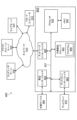
- FIG. 1 is a diagram for explaining a configuration example of a plasma processing system
- FIG. 1 is a block diagram of a computer upon which various embodiments may be implemented
- FIG. 1 is a diagram for explaining a configuration example of a capacitively coupled plasma processing apparatus
- FIG. FIG. 2 is a plan view schematically showing the outline of the configuration of an electrostatic chuck
- 4 is an enlarged plan view of the periphery of the through-hole of the electrostatic chuck according to the first embodiment
- FIG. 6 is a vertical cross-sectional view of the vicinity of the through hole shown in FIG. 5
- FIG. FIG. 11 is an enlarged plan view of the periphery of a through-hole of an electrostatic chuck according to a second embodiment
- FIG. 8 is a longitudinal sectional view around the through hole shown in FIG. 7;
- FIG. 11 is an enlarged plan view of the periphery of a through-hole of an electrostatic chuck according to a third embodiment;
- FIG. 10 is a longitudinal sectional view around the through hole shown in FIG. 9;
- FIG. 11 is a plan view schematically showing the outline of the configuration of an electrostatic chuck according to a fourth embodiment;
- FIG. 4 is an enlarged plan view of a periphery of a through hole formed in an annular region of the electrostatic chuck;
- FIG. 13 is a vertical sectional view around the through hole shown in FIG. 12;
- plasma processing is performed on a semiconductor substrate (hereinafter referred to as "substrate") in a plasma processing apparatus.
- a plasma processing apparatus generates plasma by exciting a processing gas inside a chamber, and processes a substrate supported by an electrostatic chuck with the plasma.
- a heat transfer gas such as helium gas is supplied to the space between the back surface of the substrate and the front surface of the electrostatic chuck, and the pressure of the heat transfer gas is controlled to control the temperature of the substrate.
- the electrostatic chuck is provided with through-holes for supplying the heat transfer gas. Further, for example, the electrostatic chuck is also provided with through holes through which lifter pins for transferring the substrate are inserted.
- in-plane uniformity of plasma processing can be improved by reducing the number of places where the temperature of the substrate is partially high (hereinafter referred to as “temperature singular points”). is likely to generate a temperature singularity in the substrate during plasma processing.
- the technology according to the present disclosure suppresses the occurrence of the temperature singularity of the substrate in the vicinity of the through-hole of the electrostatic chuck.
- FIG. 1 is a diagram for explaining a configuration example of a plasma processing system.
- the plasma processing system includes a plasma processing apparatus 1 and a controller 2.
- the plasma processing system is an example of a substrate processing system
- the plasma processing apparatus 1 is an example of a substrate processing apparatus.
- the plasma processing apparatus 1 includes a plasma processing chamber 10 , a substrate support section 11 and a plasma generation section 12 .
- Plasma processing chamber 10 has a plasma processing space.
- the plasma processing chamber 10 also has at least one gas inlet for supplying at least one process gas to the plasma processing space and at least one gas outlet for exhausting gas from the plasma processing space.
- the gas supply port is connected to a gas supply section 20, which will be described later, and the gas discharge port is connected to an exhaust system 40, which will be described later.
- the substrate support 11 is arranged in the plasma processing space and has a substrate support surface for supporting the substrate.
- the plasma generation unit 12 is configured to generate plasma from at least one processing gas supplied into the plasma processing space.
- Plasma formed in the plasma processing space includes capacitively coupled plasma (CCP: Capacitively Coupled Plasma), inductively coupled plasma (ICP: Inductively Coupled Plasma), ECR plasma (Electron-Cyclotron-resonance plasma), helicon wave excited plasma (HWP: Helicon Wave Plasma), surface wave plasma (SWP: Surface Wave Plasma), or the like.
- Various types of plasma generators may also be used, including alternating current (AC) plasma generators and direct current (DC) plasma generators.
- the AC signal (AC power) used in the AC plasma generator has a frequency within the range of 100 kHz to 10 GHz. Therefore, AC signals include RF (Radio Frequency) signals and microwave signals.
- the RF signal has a frequency within the range of 100 kHz-150 MHz.
- the controller 2 processes computer-executable instructions that cause the plasma processing apparatus 1 to perform the various steps described in this disclosure. Controller 2 may be configured to control elements of plasma processing apparatus 1 to perform the various processes described herein. In one embodiment, part or all of the controller 2 may be included in the plasma processing apparatus 1 .
- the control unit 2 may include a processing unit 2a1, a storage unit 2a2, and a communication interface 2a3.
- the control unit 2 is implemented by, for example, a computer 2a.
- Processing unit 2a1 can be configured to perform various control operations by reading a program from storage unit 2a2 and executing the read program. This program may be stored in the storage unit 2a2 in advance, or may be acquired via a medium when necessary.
- the acquired program is stored in the storage unit 2a2, read from the storage unit 2a2 and executed by the processing unit 2a1.
- the medium may be various storage media readable by the computer 2a, or may be a communication line connected to the communication interface 2a3.
- the processing unit 2a1 may be a CPU (Central Processing Unit).
- the storage unit 2a2 may include RAM (Random Access Memory), ROM (Read Only Memory), HDD (Hard Disk Drive), SSD (Solid State Drive), or a combination thereof.
- the communication interface 2a3 may communicate with the plasma processing apparatus 1 via a communication line such as a LAN (Local Area Network).
- FIG. 2 is a block diagram of a computer that may implement various embodiments described herein. Control aspects of the present disclosure may be embodied as systems, methods, and/or computer program products.
- the computer program product includes a computer-readable storage medium having computer-readable program instructions recorded thereon, and one or more processors may implement aspects of the embodiments.
- a computer-readable storage medium may be a tangible device capable of storing instructions for use by an instruction execution device (processor).
- Computer-readable storage media include, but are not limited to, electronic storage devices, magnetic storage devices, optical storage devices, electromagnetic storage devices, semiconductor storage devices, or any suitable combination of these devices.
- a non-exhaustive list of more specific examples of computer-readable storage media (and suitable combinations) include each of the following: floppy disk, hard disk, solid state drive (SSD), random access memory ( RAM), Read Only Memory (ROM), Programmable Read Only Memory (EPROM or Flash), Static Random Access Memory (SRAM), Compact Disc (CD or CD-ROM), Digital Versatile Disc (DVD), Memory Card Or stick.
- Computer-readable storage media as used in this disclosure include radio waves and other freely propagating electromagnetic waves, electromagnetic waves propagating through waveguides and other transmission media (e.g., light pulses passing through fiber optic cables). , or an electrical signal through a wire, etc. itself should not be construed as a transitory signal.
- the computer-readable program instructions described in this disclosure can be transferred from a computer-readable storage medium or to an external computer or storage via a global network (i.e., the Internet), local area network, wide area network and/or wireless network. It can be downloaded to a suitable computing or processing device for the apparatus. Networks may include copper wires, optical fiber, wireless transmissions, routers, firewalls, switches, gateway computers, and edge servers.
- a network adapter card or network interface in each computing or processing device receives computer readable program instructions from the network and stores the computer readable program instructions in computer readable storage within the computing or processing device. May be transferred for storage on media.
- Computer readable program instructions for performing the operations of the present disclosure include machine language instructions and/or microcode and may be written in assembly language, Basic, Fortran, Java, Python, R, C, C++, C# or similar. It can be compiled or interpreted from source code written in any combination of one or more programming languages, including programming languages.
- the computer readable program instructions may be executed entirely on a user's personal computer, notebook computer, tablet, or smart phone, or on a remote computer or computer server, or any of these computing devices. It may also be fully implemented in combination.
- the remote computer or computer server may be connected to the user's device or devices via computer networks, including local area networks, wide area networks, or global networks (the Internet).
- electronic circuits are computer readable using information from computer readable program instructions, including, for example, programmable logic circuits, field programmable gate arrays (FPGAs), or programmable logic arrays (PLAs). Execute possible program instructions to configure or customize the electronic circuitry to carry out aspects of the present disclosure.
- FPGAs field programmable gate arrays
- PLAs programmable logic arrays
- Computer readable program instructions with which the systems and methods described in this disclosure can be implemented are stored in one or more processors (and/or one within a processor) of a general purpose computer, special purpose computer, or other programmable device. above core). These computer-readable program instructions may be stored on a computer-readable storage medium capable of directing a computer, programmable apparatus, and/or other device to function in a particular manner, where , a computer-readable storage medium having instructions stored thereon, is an article of manufacture that includes instructions for implementing aspects of the functionality specified in the flow diagrams and block diagrams of this disclosure.
- the computer-readable program instructions may be loaded into a computer, other programmable device, or other device, such that the instructions executed on the computer, other programmable device, or other device , may generate a computer-implemented process by performing a series of operational steps to implement the functions specified in the flow diagrams and block diagrams of this disclosure.
- FIG. 2 is a functional block diagram illustrating a networking system 800 of one or more networked computers and servers.
- the hardware and software environment shown in FIG. 2 may provide an exemplary platform for implementation of software and/or methods according to this disclosure.
- networked system 800 may include, but is not limited to, computer 805, network 810, remote computer 815, web server 820, cloud storage server 825 and computer server 830. In some embodiments, multiple instances of one or more of the functional blocks shown in FIG. 2 may be employed.
- FIG. 805 Additional details of computer 805 are shown in FIG. The functional blocks depicted within computer 805 are provided to establish exemplary functionality only and are not intended to be exhaustive. Also, although no details are provided for remote computer 815, web server 820, cloud storage server 825 and computer server 830, these other computers and devices have similar functionality shown for computer 805. good too.
- Computer 805 may be a personal computer (PC), desktop computer, laptop computer, tablet computer, netbook computer, personal digital assistant (PDA), smart phone, or any other programmable electronic device capable of communicating with other devices on network 810. can be a device.
- PC personal computer
- PDA personal digital assistant
- smart phone or any other programmable electronic device capable of communicating with other devices on network 810.
- Computer 805 may include processor 835 , bus 837 , memory 840 , nonvolatile storage 845 , network interface 850 , peripherals interface 855 and display interface 865 .
- processor 835 bus 837
- memory 840 nonvolatile storage 845
- network interface 850 network interface 850
- peripherals interface 855 display interface 865 .
- Each of these functions may be implemented in some embodiments as individual electronic subsystems (an integrated circuit chip or combination of chips and associated devices), or in other embodiments some combination of functions may be implemented in a single on a chip (sometimes called a chip-on-system or SoC).
- Processor 835 may be one or more single or multi-chip microprocessors.
- Bus 837 can be any proprietary standard high speed parallel or serial peripheral interconnect bus such as ISA, PCI, PCI Express (PCI-e), AGP, or the like.
- Memory 840 and non-volatile storage 845 can be computer-readable storage media.
- Memory 840 may include any suitable volatile storage such as dynamic random access memory (DRAM) and static random access memory (SRAM).
- Non-volatile storage 845 can be floppy disk, hard disk, solid state drive (SSD), read only memory (ROM), programmable read only memory (EPROM or Flash), compact disk (CD or CD-ROM), digital general purpose disk. (DVD) and one or more of memory cards or sticks.
- Programs 848 are machine-readable programs stored in nonvolatile storage 845 and used to create, manage, and control certain software functions that are described in detail elsewhere in this disclosure and illustrated in the drawings. It may be a set of possible instructions and/or data. In some embodiments, memory 840 may be significantly faster than non-volatile storage 845 . In such embodiments, programs 848 may be transferred from nonvolatile storage 845 to memory 840 before being executed by processor 835 .
- Network 810 may include, for example, a local area network (LAN), a wide area network (WAN) such as the Internet, or a combination of both, wired, wireless, or fiber optic connections.
- LAN local area network
- WAN wide area network
- network 810 can be any combination of connections and protocols that support communication between two or more computers and associated devices.
- Peripherals interface 855 may allow input and output of data with other devices that may be locally connected to computer 805 .
- peripherals interface 855 may provide connectivity to external devices 860 .
- External devices 860 may include devices such as keyboards, mice, keypads, touch screens, and/or other suitable input devices.
- External devices 860 may also include portable computer-readable storage media such as, for example, thumb drives, portable or magnetic disks, and memory cards.
- Software and data used in embodiments of the present disclosure may be stored, for example, in program 848, portable computer-readable storage media, and the like. In such embodiments, the software may be loaded into non-volatile storage 845 or, alternatively, loaded directly into memory 840 via peripheral interface 855 .
- Peripheral interface 855 may connect to external devices 860 using industry standard connections such as RS-232 or Universal Serial Bus (USB).
- a display interface 865 may connect the computer 805 to the display 870 .
- Display 870 may be used in some embodiments to present a command line or graphical user interface to a user of computer 805 .
- Display interface 865 may connect to display 870 using one or more proprietary or industry standard connections such as VGA, DVI, DisplayPort, HDMI.
- network interface 850 provides communication with other computing and storage systems or devices external to computer 805 .
- the software programs and data described herein may be downloaded to non-volatile storage 845 via network interface 850 and network 810 from remote computers 815 , web servers 820 , cloud storage servers 825 and computer servers 830 , for example.
- the systems and methods described in this disclosure can be performed by one or more computers connected to computer 805 via network interface 850 and network 810 .
- the systems and methods described in this disclosure may be performed by remote computer 815 , computer server 830 , or a combination of interconnected computers on network 810 .
- Data, datasets and/or databases used in examples of implementation of the systems and methods described in this disclosure may be stored or downloaded from remote computers 815, web servers 820, cloud storage servers 825 and computer servers 830. .
- FIG. 3 is a diagram for explaining a configuration example of a capacitively coupled plasma processing apparatus.
- FIG. 4 is a plan view schematically showing the outline of the configuration of the electrostatic chuck.
- the capacitively coupled plasma processing apparatus 1 includes a plasma processing chamber 10, a gas supply section 20, a power supply 30 and an exhaust system 40.
- the plasma processing apparatus 1 also includes a substrate supporter 11 as an example of a substrate supporter and a gas inlet.
- the gas introduction is configured to introduce at least one process gas into the plasma processing chamber 10 .
- the gas introduction section includes a showerhead 13 .
- a substrate support 11 is positioned within the plasma processing chamber 10 .
- the showerhead 13 is arranged above the substrate support 11 .
- showerhead 13 forms at least a portion of the ceiling of plasma processing chamber 10 .
- the plasma processing chamber 10 has a plasma processing space 10 s defined by a showerhead 13 , side walls 10 a of the plasma processing chamber 10 and a substrate support 11 .
- Plasma processing chamber 10 is grounded.
- the showerhead 13 and substrate support 11 are electrically insulated from the housing of the plasma processing chamber 10 .
- the substrate support section 11 includes a body section 111 and a ring assembly 112 .
- the body portion 111 has a central region 111 a for supporting the substrate W and an annular region 111 b for supporting the ring assembly 112 .
- a wafer is an example of a substrate W;
- the annular region 111b of the body portion 111 surrounds the central region 111a of the body portion 111 in plan view.
- the substrate W is arranged on the central region 111 a of the main body 111
- the ring assembly 112 is arranged on the annular region 111 b of the main body 111 so as to surround the substrate W on the central region 111 a of the main body 111 .
- the central region 111a is also referred to as a substrate support surface for supporting the substrate W
- the annular region 111b is also referred to as a ring support surface for supporting the ring assembly 112.
- the body portion 111 includes a base 1110 and an electrostatic chuck 1111 .
- the base 1110 includes a conductive member such as aluminum and has a substantially disk shape.
- a conductive member of the base 1110 can function as a bottom electrode.
- the electrostatic chuck 1111 is formed by thermally spraying a sintered body of an insulating material such as ceramic or an insulating material.
- the electrostatic chuck 1111 is arranged on the base 1110 via the bonding layer.
- the bonding layer is made of a material having plasma resistance and heat resistance. For example, acrylic resin, silicon resin, epoxy resin, or the like can be used.
- the electrostatic chuck 1111 includes an insulating member 1111a, a first electrostatic electrode 1111b disposed within the insulating member 1111a, and a second electrostatic electrode 1111c.
- the insulating member 1111a has a central region 111a.
- the insulating member 1111a also has an annular region 111b.
- the central region 111a and the annular region 111b may be formed integrally or may be formed separately.
- the first electrostatic electrode 1111b is used as an electrode for electrostatically attracting the substrate W supported by the central region 111a, for example.
- the second electrostatic electrode 1111c is used, for example, as an electrode for electrostatically attracting the ring assembly 112 supported by the annular region 111b surrounding the central region 111a.
- another member surrounding electrostatic chuck 1111 such as an annular electrostatic chuck or an annular insulating member, may have annular region 111b.
- the ring assembly 112 may be placed on the annular electrostatic chuck or the annular insulating member, or may be placed on both the electrostatic chuck 1111 and the annular insulating member.
- at least one RF/DC electrode coupled to an RF power source 31 and/or a DC power source 32, described below, may be disposed within the insulating member 1111a. In this case, at least one RF/DC electrode functions as the bottom electrode.
- the RF/DC electrode is also called a bias electrode.
- the conductive member of the base 1110 and at least one RF/DC electrode may function as a plurality of lower electrodes.
- the first electrostatic electrode 1111b may function as a lower electrode.
- the substrate support 11 includes at least one bottom electrode.
- Ring assembly 112 includes one or more annular members.
- the one or more annular members include one or more edge rings and at least one cover ring.
- the edge ring is made of a conductive material or an insulating material
- the cover ring is made of an insulating material.
- the substrate supporter 11 may include a temperature control module configured to adjust at least one of the electrostatic chuck 1111, the ring assembly 112, and the substrate to a target temperature.
- the temperature control module may include heaters, heat transfer media, channels 1110a, or combinations thereof.
- channels 1110a are formed in base 1110 and one or more heaters are disposed in insulating members 1111a of electrostatic chuck 1111 .
- the substrate support section 11 may include a heat transfer gas supply section 50 configured to supply a heat transfer gas to the gap between the back surface of the substrate W and the central region 111a.
- the heat transfer gas supply unit 50 supplies heat transfer gas to the plurality of gas supply holes 120 a ( FIG. 4 ) formed in the electrostatic chuck 1111 through the gas supply path 51 .
- the gas supply hole 120a is a through hole that penetrates the electrostatic chuck 1111 in the vertical direction.
- the plurality of gas supply holes 120a are spaced apart from each other and arranged concentrically around the center of the circular central region 111a.
- the gas supply hole 120a can also be used as a hole for exhausting heat transfer gas between the back surface of the substrate W and the central region 111a.
- the electrostatic chuck 1111 has a plurality of first pin insertion holes 120b (FIG. 4) as other through holes in the central region 111a.
- the first pin insertion holes 120b are through holes through which the first lifter pins 60 for supporting and lifting the substrate W are inserted, and extend in the vertical direction.
- the plurality of first pin through holes 120b are spaced apart from each other, and each of the first pin through holes 120b has the same diameter with the center of the circular central region 111a as the center of the circle. arranged on a circle.
- the first lifter pin 60 is configured to be movable up and down by being connected to the drive section 61 .
- the driving unit 61 has, for example, a motor (not shown) that generates a lifting driving force.
- the electrostatic chuck 1111 has a plurality of second pin insertion holes 120c (FIG. 4) as other through holes in the annular region 111b.
- the second pin insertion holes 120c are through holes through which the second lifter pins 70 for supporting and lifting the ring assembly 112 are inserted, and extend in the vertical direction.
- the plurality of second pin through holes 120c are spaced apart from each other, and each of the second pin through holes 120c has the same diameter with the center of the circular annular region 111b as the center of the circle. arranged on a circle.
- the second lifter pin 70 is configured to be movable up and down by being connected to the drive section 71 .
- the driving unit 71 has, for example, a motor (not shown) that generates a lifting driving force.
- the electrostatic chuck 1111 has a substrate contact portion 130 ( FIG. 4 ) with a plurality of protrusions 131 .
- a plurality of protrusions 131 are arranged in the central region 111a and protrude upward from the central region 111a.
- a space is formed between the substrate W and the central region 111a by the protrusions 131 coming into contact with the back surface of the substrate W, and the heat transfer gas diffuses in this space.
- the showerhead 13 is configured to introduce at least one processing gas from the gas supply unit 20 into the plasma processing space 10s.
- the showerhead 13 has at least one gas supply port 13a, at least one gas diffusion chamber 13b, and multiple gas introduction ports 13c.
- the processing gas supplied to the gas supply port 13a passes through the gas diffusion chamber 13b and is introduced into the plasma processing space 10s through a plurality of gas introduction ports 13c.
- showerhead 13 also includes at least one upper electrode.
- the gas introduction part may include one or more side gas injectors (SGI: Side Gas Injector) attached to one or more openings formed in the side wall 10a.
- SGI Side Gas Injector
- the gas supply unit 20 may include at least one gas source 21 and at least one flow controller 22 .
- gas supply 20 is configured to supply at least one process gas from respective gas sources 21 through respective flow controllers 22 to showerhead 13 .
- Each flow controller 22 may include, for example, a mass flow controller or a pressure controlled flow controller.
- gas supply 20 may include at least one flow modulation device for modulating or pulsing the flow rate of at least one process gas.
- Power supply 30 includes an RF power supply 31 coupled to plasma processing chamber 10 via at least one impedance matching circuit.
- RF power supply 31 is configured to supply at least one RF signal (RF power) to at least one lower electrode and/or at least one upper electrode.
- RF power supply 31 can function as at least part of the plasma generator 12 .
- a bias RF signal to at least one lower electrode, a bias potential is generated in the substrate W, and ion components in the formed plasma can be drawn into the substrate W.
- the RF power supply 31 includes a first RF generator 31a and a second RF generator 31b.
- the first RF generator 31a is coupled to at least one lower electrode and/or at least one upper electrode via at least one impedance matching circuit to generate a source RF signal (source RF power) for plasma generation.
- the source RF signal has a frequency within the range of 10 MHz to 150 MHz.
- the first RF generator 31a may be configured to generate multiple source RF signals having different frequencies.
- One or more source RF signals generated are provided to at least one bottom electrode and/or at least one top electrode.
- the second RF generator 31b is coupled to at least one lower electrode via at least one impedance matching circuit and configured to generate a bias RF signal (bias RF power).
- the frequency of the bias RF signal may be the same as or different from the frequency of the source RF signal.
- the bias RF signal has a frequency lower than the frequency of the source RF signal.
- the bias RF signal has a frequency within the range of 100 kHz to 60 MHz.
- the second RF generator 31b may be configured to generate multiple bias RF signals having different frequencies.
- One or more bias RF signals generated are provided to at least one bottom electrode. Also, in various embodiments, at least one of the source RF signal and the bias RF signal may be pulsed.
- Power supply 30 may also include a DC power supply 32 coupled to plasma processing chamber 10 .
- the DC power supply 32 includes a first DC generator 32a and a second DC generator 32b.
- the first DC generator 32a is connected to the at least one bottom electrode and configured to generate a first DC signal.
- the generated first DC signal is applied to at least one bottom electrode.
- the second DC generator 32b is connected to the at least one top electrode and configured to generate a second DC signal.
- the generated second DC signal is applied to at least one top electrode.
- the first and second DC signals may be pulsed.
- a sequence of voltage pulses is applied to at least one bottom electrode and/or at least one top electrode.
- the voltage pulses may have rectangular, trapezoidal, triangular, or combinations thereof pulse waveforms.
- a waveform generator for generating a sequence of voltage pulses from a DC signal is connected between the first DC generator 32a and the at least one bottom electrode. Therefore, the first DC generator 32a and the waveform generator constitute a voltage pulse generator.
- the second DC generator 32b and the waveform generator constitute a voltage pulse generator, the voltage pulse generator is connected to at least one upper electrode.
- the voltage pulse may have a positive polarity or a negative polarity.
- the sequence of voltage pulses may include one or more positive voltage pulses and one or more negative voltage pulses in one cycle.
- the first and second DC generators 32a and 32b may be provided in addition to the RF power supply 31, and the first DC generator 32a may be provided instead of the second RF generator 31b. good.
- the exhaust system 40 may be connected to a gas exhaust port 10e provided at the bottom of the plasma processing chamber 10, for example.
- Exhaust system 40 may include a pressure regulating valve and a vacuum pump.
- the pressure regulating valve regulates the pressure in the plasma processing space 10s.
- Vacuum pumps may include turbomolecular pumps, dry pumps, or combinations thereof.
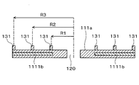
- FIG. 5 is an enlarged plan view of the vicinity of the through hole of the electrostatic chuck according to the first embodiment.
- FIG. 6 is a longitudinal sectional view around the through hole shown in FIG.
- ten protrusions 131 are arranged at positions with a radius R1 from the center of the through hole 120 (for example, the gas supply hole 120a and the first pin insertion hole 120b shown in FIG. 4).
- Ten projections 131 are arranged at a radius R2 from the center of the through-hole 120, and 16 projections 131 are arranged at a radius R3 from the center of the through-hole 120.
- FIG. Each protrusion 131 is arranged concentrically with the center of the through hole 120 as the center of the circle.
- the radius R1 is, for example, 3.9 mm.
- the radius R1 is, for example, 3.55 mm.
- a preferred distance from the through-hole 120 to each projection 131 is appropriately changed according to the positional relationship between the through-hole 120 and the first electrostatic electrode 1111b.
- the density of the projections 131 differs in the radial direction of the through-hole 120 .
- the “protrusion density” in this specification is the number of protrusions 131 per unit area.
- the number of protrusions 131 per unit area in the area from the center of the through-hole 120 to the position of radius R1 is the number of protrusions 131 per unit area in the area from the position of radius R1 to the position of radius R3.
- the substrate contact portion 130 according to the present embodiment includes a first substrate contact portion 130a and a second substrate contact portion 130b having different densities of the protrusions 131 in the radial direction of the through hole 120.
- the first substrate contact portion 130a is arranged around the through-hole 120, and the second substrate contact portion 130b is arranged around the first substrate contact portion 130a.
- the density of the protrusions 131 in the first substrate contact portion 130a is defined as the first density
- the protrusions 131 are arranged in the second substrate contact portion 130b at a second density lower than the first density.
- the electrostatic chuck 1111 according to the present embodiment has the first substrate contact portion 130a in which the projections 131 are arranged at a first density, and the projections 131 are arranged at a second density lower than the first density. and a second substrate contact portion 130b.
- the cooling ability of the substrate W in the vicinity of the through hole 120 can be locally increased. can be enhanced. This makes it possible to suppress a local temperature rise of the substrate W in the vicinity of the through-hole 120 during plasma processing. That is, according to the electrostatic chuck 1111 according to this embodiment, it is possible to suppress the generation of the temperature singularity of the substrate W near the through hole 120 .
- the arrangement of the projections 131 and the number of the projections 131 are not particularly limited as long as the condition that the second density is smaller than the first density is satisfied. Further, for example, the projections 131 do not have to be arranged concentrically. However, the localized temperature rise region of the substrate W in the vicinity of the through hole 120 tends to be circular. Therefore, from the viewpoint of uniformly cooling the localized temperature rise region of the substrate W, the projections 131 of the first substrate contact portion 130a should be arranged concentrically with the center of the through-hole 120 as the center of the circle. is preferred.
- At least part of the first substrate contact portion 130 a is preferably located above the first electrostatic electrode 1111 b provided inside the electrostatic chuck 1111 . Accordingly, the attraction force of the first substrate contact portion 130a to the substrate W can be increased, and the contact area of the first substrate contact portion 130a to the substrate W can be increased. As a result, the amount of heat transferred from the substrate W to the first substrate contact portion 130a by thermal conduction increases, and local temperature rise of the substrate W can be effectively suppressed.
- FIG. 7 is an enlarged plan view of the periphery of the through-hole of the electrostatic chuck according to the second embodiment.
- FIG. 8 is a vertical sectional view around the through hole shown in FIG.
- the first substrate contact portion 130a in this embodiment has a projection 131a (hereinafter referred to as "end projection”) arranged above the end of the first electrostatic electrode 1111b on the through hole 120 side.
- Ten end protrusions 131 a are arranged at positions with a radius R ⁇ b>1 from the center of the through hole 120 .
- the first substrate contact portion 130a includes a projection 131b (hereinafter referred to as an “inner projection”) arranged radially inside the through hole 120 (center side of the through hole 120) with respect to the end projection 131a. have.
- Six inner protrusions 131b are arranged at positions with a radius R4 from the center of the through-hole 120. As shown in FIG.
- Each protrusion 131 is arranged concentrically with the center of the through hole 120 as the center of the circle.
- the radius R1 is, for example, 3.9 mm
- the radius R4 is, for example, 2.5 mm.
- the radius R1 is, for example, 3.55 mm
- the radius R4 is, for example, 1.78 mm.
- a preferable distance of each projection 131 including the end projection 131a and the inner projection 131b from the through hole 120 is appropriately changed according to the positional relationship between the through hole 120 and the first electrostatic electrode 1111b.
- the density of the projections 131 arranged on the first substrate contact portion 130a is higher than the density of the projections 131 arranged on the second substrate contact portion 130b. Therefore, the cooling capacity of the substrate W in the first substrate contact portion 130a is relatively high compared to that in the second substrate contact portion 130b.
- the inner protrusion 131b is provided on the first substrate contact portion 130a, the cooling capability of the substrate W in the first substrate contact portion 130a is improved. Therefore, according to the electrostatic chuck 1111 according to this embodiment, it becomes easier to suppress the local temperature rise of the substrate W in the vicinity of the through hole 120 .
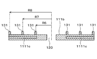
- FIG. 9 is an enlarged plan view of the periphery of the through-hole of the electrostatic chuck according to the third embodiment.
- FIG. 10 is a vertical sectional view around the through hole shown in FIG.
- the first substrate contact portion 130a in the present embodiment is a protrusion 131c (hereinafter referred to as " (referred to as "outer projection”).
- 16 outer protrusions 131c are arranged at a radius R5 from the center of the through-hole 120 .
- Each protrusion 131 is arranged concentrically with the center of the through hole 120 as the center of the circle.
- the radius R1 is, for example, 3.9 mm
- the radius R5 is, for example, 6.2 mm.
- the radius R1 is, for example, 3.55 mm
- the radius R5 is, for example, 5.85 mm.
- a preferable distance of each projection 131 including the end projection 131a and the outer projection 131c from the through hole 120 is appropriately changed according to the positional relationship between the through hole 120 and the first electrostatic electrode 1111b.
- the density of the projections 131 arranged on the first substrate contact portion 130a is higher than the density of the projections 131 arranged on the second substrate contact portion 130b. Therefore, the cooling capacity of the substrate W in the first substrate contact portion 130a is relatively high compared to that in the second substrate contact portion 130b. In addition, since the first substrate contact portion 130a is provided with the outer projection 131c, the cooling capability of the substrate W in the first substrate contact portion 130a is improved. Therefore, according to the electrostatic chuck 1111 according to this embodiment, it becomes easier to suppress the local temperature rise of the substrate W in the vicinity of the through hole 120 .
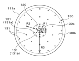
- FIG. 11 is a plan view schematically showing the outline of the configuration of the electrostatic chuck according to the fourth embodiment.
- FIG. 12 is an enlarged plan view of the vicinity of the through hole formed in the annular region of the electrostatic chuck.
- 13 is a longitudinal sectional view around the through hole shown in FIG. 12.
- the electrostatic chuck 1111 has a ring contact portion 132 in the annular region 111b in addition to the substrate contact portion 130.
- the ring contact portion 132 has a plurality of projections 131 projecting upward from the annular region 111b.
- Ten protrusions 131 of the annular region 111b are arranged at a radius R6 from the center of the through hole 120 (for example, the second pin insertion hole 120c shown in FIG. 11).
- Ten projections 131 are arranged at a radius R7 from the center of the through-hole 120, and 16 projections 131 are arranged at a radius R8 from the center of the through-hole 120.
- Each protrusion 131 is arranged concentrically with the center of the through hole 120 as the center of the circle. A preferred distance from the through-hole 120 to each projection 131 is appropriately changed according to the positional relationship between the through-hole 120 and the second electrostatic electrode 1111c.
- the ring contact portion 132 in which the projections 131 are arranged as described above has a first ring contact portion 132a and a second ring contact portion 132b in which the density of the projections 131 in the radial direction of the through hole 120 is different.
- the first ring contact portion 132a is arranged around the through hole 120
- the second ring contact portion 132b is arranged around the first ring contact portion 132a.
- the density of the projections 131 in the first ring contact portion 132a is defined as the third density
- the projections 131 are arranged in the second ring contact portion 132b at a fourth density lower than the third density.
- the electrostatic chuck 1111 has the first ring contact portion 132a in which the projections 131 are arranged at a third density, and the projections 131 are arranged at a fourth density lower than the third density. and a second ring contact portion 132b.
- the first ring contact portion 132a having a higher density of protrusions 131 than the second ring contact portion 132b exists around the through hole 120.
- FIG. Therefore, the cooling capacity of the ring assembly 112 in the vicinity of the through hole 120 can be locally enhanced. This makes it possible to suppress a local temperature rise in the ring assembly 112 that may occur in the vicinity of the through hole 120 during plasma processing, and suppress the occurrence of a temperature singularity at the peripheral edge of the substrate W.
- the arrangement of the projections 131 in the ring contact portion 132 and the number of the projections 131 are not particularly limited.
- the inner projection 131b and the outer projection 131c described in the second and third embodiments may be applied to the ring contact portion 132.
- the shape of the protrusion 131 in plan view is not particularly limited, and may be a circular shape, a triangular shape, a square shape, or any other shape.
- the protrusions 131 have a diameter of, for example, 0.2-1.0 mm.
- Each protrusion 131 may not have the same shape.
- the height of each protrusion 131 (the height from the central region 111a or the annular region 111b to the upper end of the protrusion 131) may not be the same height.
- the first density and the third density may be the same or different, and the second density and the fourth density may be the same or different.
- the gas supply hole 120a, the first pin insertion hole 120b, and the second pin insertion hole 120c are exemplified as the uses of the through holes 120, but the uses of the through holes 120 are not particularly limited.
- the through hole 120 may be a hole for inserting a temperature sensor for substrate temperature measurement.
- the number of through-holes is not particularly limited, and even if there is only one through-hole, if the electrostatic chuck 1111 as described in the above-described embodiment is applied to the through-hole, the The effect of suppressing the generation of the temperature singularity of the substrate W can be obtained.
- plasma processing apparatus 10 plasma processing chamber 11 substrate supporting portion 111a central region 120 through hole 130a first substrate contact portion 130b second substrate contact portion 131 protrusion 1110 base 1111 electrostatic chuck W substrate
Landscapes
- Chemical & Material Sciences (AREA)
- Physics & Mathematics (AREA)
- Engineering & Computer Science (AREA)
- Plasma & Fusion (AREA)
- Metallurgy (AREA)
- Mechanical Engineering (AREA)
- Materials Engineering (AREA)
- Organic Chemistry (AREA)
- Chemical Kinetics & Catalysis (AREA)
- Electromagnetism (AREA)
- General Chemical & Material Sciences (AREA)
- Spectroscopy & Molecular Physics (AREA)
- Analytical Chemistry (AREA)
- Drying Of Semiconductors (AREA)
- Container, Conveyance, Adherence, Positioning, Of Wafer (AREA)
Priority Applications (4)
| Application Number | Priority Date | Filing Date | Title |
|---|---|---|---|
| CN202280055398.1A CN117795657A (zh) | 2021-08-20 | 2022-08-08 | 静电卡盘、基片支承器和基片处理装置 |
| KR1020247007666A KR20240051154A (ko) | 2021-08-20 | 2022-08-08 | 정전 척, 기판 지지기 및 기판 처리 장치 |
| JP2023542347A JPWO2023022041A1 (https=) | 2021-08-20 | 2022-08-08 | |
| US18/443,834 US20240186917A1 (en) | 2021-08-20 | 2024-02-16 | Electrostatic chuck, substrate support, and substrate processing apparatus |
Applications Claiming Priority (4)
| Application Number | Priority Date | Filing Date | Title |
|---|---|---|---|
| US202163235231P | 2021-08-20 | 2021-08-20 | |
| US63/235,231 | 2021-08-20 | ||
| JP2021148145 | 2021-09-10 | ||
| JP2021-148145 | 2021-09-10 |
Related Child Applications (1)
| Application Number | Title | Priority Date | Filing Date |
|---|---|---|---|
| US18/443,834 Continuation US20240186917A1 (en) | 2021-08-20 | 2024-02-16 | Electrostatic chuck, substrate support, and substrate processing apparatus |
Publications (1)
| Publication Number | Publication Date |
|---|---|
| WO2023022041A1 true WO2023022041A1 (ja) | 2023-02-23 |
Family
ID=85240649
Family Applications (1)
| Application Number | Title | Priority Date | Filing Date |
|---|---|---|---|
| PCT/JP2022/030261 Ceased WO2023022041A1 (ja) | 2021-08-20 | 2022-08-08 | 静電チャック、基板支持器及び基板処理装置 |
Country Status (5)
| Country | Link |
|---|---|
| US (1) | US20240186917A1 (https=) |
| JP (1) | JPWO2023022041A1 (https=) |
| KR (1) | KR20240051154A (https=) |
| TW (1) | TW202316542A (https=) |
| WO (1) | WO2023022041A1 (https=) |
Cited By (2)
| Publication number | Priority date | Publication date | Assignee | Title |
|---|---|---|---|---|
| WO2025004883A1 (ja) * | 2023-06-29 | 2025-01-02 | 東京エレクトロン株式会社 | プラズマ処理装置 |
| EP4621094A1 (en) * | 2024-03-21 | 2025-09-24 | ASM IP Holding B.V. | Susceptors, semiconductor processings systems, and related methods |
Citations (7)
| Publication number | Priority date | Publication date | Assignee | Title |
|---|---|---|---|---|
| JPH10233433A (ja) * | 1996-01-31 | 1998-09-02 | Canon Inc | 基板の保持装置とこれを用いた露光装置、及びデバイスの製造方法 |
| US6320736B1 (en) * | 1999-05-17 | 2001-11-20 | Applied Materials, Inc. | Chuck having pressurized zones of heat transfer gas |
| JP2005191561A (ja) * | 2003-12-05 | 2005-07-14 | Tokyo Electron Ltd | 静電チャック |
| JP2006257495A (ja) * | 2005-03-17 | 2006-09-28 | Tokyo Electron Ltd | 基板保持部材及び基板処理装置 |
| JP2013153171A (ja) * | 2013-02-15 | 2013-08-08 | Panasonic Corp | プラズマ処理装置及びプラズマ処理方法 |
| US20160035610A1 (en) * | 2014-07-30 | 2016-02-04 | Myoung Soo Park | Electrostatic chuck assemblies having recessed support surfaces, semiconductor fabricating apparatuses having the same, and plasma treatment methods using the same |
| JP2016510167A (ja) * | 2013-02-13 | 2016-04-04 | インテグリス・インコーポレーテッド | ポリマー性エンボスを備える真空チャック |
Family Cites Families (6)
| Publication number | Priority date | Publication date | Assignee | Title |
|---|---|---|---|---|
| JP3983387B2 (ja) * | 1998-09-29 | 2007-09-26 | 日本碍子株式会社 | 静電チャック |
| KR100511854B1 (ko) * | 2002-06-18 | 2005-09-02 | 아네르바 가부시키가이샤 | 정전 흡착 장치 |
| JP4061131B2 (ja) * | 2002-06-18 | 2008-03-12 | キヤノンアネルバ株式会社 | 静電吸着装置 |
| KR20040070008A (ko) * | 2003-01-29 | 2004-08-06 | 쿄세라 코포레이션 | 정전척 |
| JP4636807B2 (ja) * | 2004-03-18 | 2011-02-23 | キヤノン株式会社 | 基板保持装置およびそれを用いた露光装置 |
| JP6948822B2 (ja) | 2017-04-25 | 2021-10-13 | 東京エレクトロン株式会社 | 基板処理装置及び基板取り外し方法 |
-
2022
- 2022-08-08 WO PCT/JP2022/030261 patent/WO2023022041A1/ja not_active Ceased
- 2022-08-08 JP JP2023542347A patent/JPWO2023022041A1/ja active Pending
- 2022-08-08 KR KR1020247007666A patent/KR20240051154A/ko active Pending
- 2022-08-15 TW TW111130537A patent/TW202316542A/zh unknown
-
2024
- 2024-02-16 US US18/443,834 patent/US20240186917A1/en active Pending
Patent Citations (7)
| Publication number | Priority date | Publication date | Assignee | Title |
|---|---|---|---|---|
| JPH10233433A (ja) * | 1996-01-31 | 1998-09-02 | Canon Inc | 基板の保持装置とこれを用いた露光装置、及びデバイスの製造方法 |
| US6320736B1 (en) * | 1999-05-17 | 2001-11-20 | Applied Materials, Inc. | Chuck having pressurized zones of heat transfer gas |
| JP2005191561A (ja) * | 2003-12-05 | 2005-07-14 | Tokyo Electron Ltd | 静電チャック |
| JP2006257495A (ja) * | 2005-03-17 | 2006-09-28 | Tokyo Electron Ltd | 基板保持部材及び基板処理装置 |
| JP2016510167A (ja) * | 2013-02-13 | 2016-04-04 | インテグリス・インコーポレーテッド | ポリマー性エンボスを備える真空チャック |
| JP2013153171A (ja) * | 2013-02-15 | 2013-08-08 | Panasonic Corp | プラズマ処理装置及びプラズマ処理方法 |
| US20160035610A1 (en) * | 2014-07-30 | 2016-02-04 | Myoung Soo Park | Electrostatic chuck assemblies having recessed support surfaces, semiconductor fabricating apparatuses having the same, and plasma treatment methods using the same |
Cited By (2)
| Publication number | Priority date | Publication date | Assignee | Title |
|---|---|---|---|---|
| WO2025004883A1 (ja) * | 2023-06-29 | 2025-01-02 | 東京エレクトロン株式会社 | プラズマ処理装置 |
| EP4621094A1 (en) * | 2024-03-21 | 2025-09-24 | ASM IP Holding B.V. | Susceptors, semiconductor processings systems, and related methods |
Also Published As
| Publication number | Publication date |
|---|---|
| US20240186917A1 (en) | 2024-06-06 |
| TW202316542A (zh) | 2023-04-16 |
| KR20240051154A (ko) | 2024-04-19 |
| JPWO2023022041A1 (https=) | 2023-02-23 |
Similar Documents
| Publication | Publication Date | Title |
|---|---|---|
| TW202205513A (zh) | 基板支持器及電漿處理裝置 | |
| US20240186917A1 (en) | Electrostatic chuck, substrate support, and substrate processing apparatus | |
| US20240194514A1 (en) | Substrate support and substrate processing apparatus | |
| US20250014874A1 (en) | Electrostatic chuck and plasma processing apparatus | |
| CN117916862A (zh) | 基片支承器和基片处理装置 | |
| US12406853B2 (en) | Etching method and plasma processing apparatus | |
| KR102905047B1 (ko) | 플라즈마 처리 장치, 전원 시스템, 및 주파수 제어 방법 | |
| US12563979B2 (en) | Etching method and plasma processing apparatus | |
| WO2024171714A1 (ja) | プラズマ処理装置 | |
| CN117795657A (zh) | 静电卡盘、基片支承器和基片处理装置 | |
| US20250246416A1 (en) | Substrate support and plasma processing apparatus | |
| CN117678062A (zh) | 基片支承器和基片处理装置 | |
| TWI918979B (zh) | 基板支持器及基板處理裝置 | |
| TW202431524A (zh) | 基板處理裝置及靜電吸盤 | |
| US20240339303A1 (en) | Substrate support and plasma processing apparatus | |
| WO2023008209A1 (ja) | 基板支持器及び基板処理装置 | |
| WO2026074929A1 (ja) | プラズマ処理装置及びプラズマ処理方法 | |
| JP2024094874A (ja) | プラズマ処理装置 | |
| KR20250134622A (ko) | 지지체, 기판 지지기 및 플라즈마 처리 장치 | |
| KR20250165342A (ko) | 에칭 장치 및 에칭 방법 | |
| WO2026053764A1 (ja) | プラズマ処理装置、電源システム、及びプラズマ処理方法 | |
| WO2026034197A1 (ja) | プラズマ処理装置及びプラズマ処理方法 | |
| TW202341228A (zh) | 電漿處理裝置 |
Legal Events
| Date | Code | Title | Description |
|---|---|---|---|
| 121 | Ep: the epo has been informed by wipo that ep was designated in this application |
Ref document number: 22858362 Country of ref document: EP Kind code of ref document: A1 |
|
| WWE | Wipo information: entry into national phase |
Ref document number: 2023542347 Country of ref document: JP |
|
| WWE | Wipo information: entry into national phase |
Ref document number: 202280055398.1 Country of ref document: CN |
|
| ENP | Entry into the national phase |
Ref document number: 20247007666 Country of ref document: KR Kind code of ref document: A |
|
| NENP | Non-entry into the national phase |
Ref country code: DE |
|
| 122 | Ep: pct application non-entry in european phase |
Ref document number: 22858362 Country of ref document: EP Kind code of ref document: A1 |