WO2023021632A1 - 光学素子、撮像素子及び撮像装置 - Google Patents
光学素子、撮像素子及び撮像装置 Download PDFInfo
- Publication number
- WO2023021632A1 WO2023021632A1 PCT/JP2021/030262 JP2021030262W WO2023021632A1 WO 2023021632 A1 WO2023021632 A1 WO 2023021632A1 JP 2021030262 W JP2021030262 W JP 2021030262W WO 2023021632 A1 WO2023021632 A1 WO 2023021632A1
- Authority
- WO
- WIPO (PCT)
- Prior art keywords
- layer
- structures
- light
- pixel
- optical element
- Prior art date
- Legal status (The legal status is an assumption and is not a legal conclusion. Google has not performed a legal analysis and makes no representation as to the accuracy of the status listed.)
- Ceased
Links
Images









Classifications
-
- H—ELECTRICITY
- H10—SEMICONDUCTOR DEVICES; ELECTRIC SOLID-STATE DEVICES NOT OTHERWISE PROVIDED FOR
- H10F—INORGANIC SEMICONDUCTOR DEVICES SENSITIVE TO INFRARED RADIATION, LIGHT, ELECTROMAGNETIC RADIATION OF SHORTER WAVELENGTH OR CORPUSCULAR RADIATION
- H10F39/00—Integrated devices, or assemblies of multiple devices, comprising at least one element covered by group H10F30/00, e.g. radiation detectors comprising photodiode arrays
- H10F39/80—Constructional details of image sensors
- H10F39/805—Coatings
- H10F39/8053—Colour filters
-
- G—PHYSICS
- G02—OPTICS
- G02B—OPTICAL ELEMENTS, SYSTEMS OR APPARATUS
- G02B5/00—Optical elements other than lenses
-
- H—ELECTRICITY
- H10—SEMICONDUCTOR DEVICES; ELECTRIC SOLID-STATE DEVICES NOT OTHERWISE PROVIDED FOR
- H10F—INORGANIC SEMICONDUCTOR DEVICES SENSITIVE TO INFRARED RADIATION, LIGHT, ELECTROMAGNETIC RADIATION OF SHORTER WAVELENGTH OR CORPUSCULAR RADIATION
- H10F39/00—Integrated devices, or assemblies of multiple devices, comprising at least one element covered by group H10F30/00, e.g. radiation detectors comprising photodiode arrays
- H10F39/10—Integrated devices
- H10F39/12—Image sensors
-
- H—ELECTRICITY
- H10—SEMICONDUCTOR DEVICES; ELECTRIC SOLID-STATE DEVICES NOT OTHERWISE PROVIDED FOR
- H10F—INORGANIC SEMICONDUCTOR DEVICES SENSITIVE TO INFRARED RADIATION, LIGHT, ELECTROMAGNETIC RADIATION OF SHORTER WAVELENGTH OR CORPUSCULAR RADIATION
- H10F39/00—Integrated devices, or assemblies of multiple devices, comprising at least one element covered by group H10F30/00, e.g. radiation detectors comprising photodiode arrays
- H10F39/80—Constructional details of image sensors
- H10F39/802—Geometry or disposition of elements in pixels, e.g. address-lines or gate electrodes
-
- H—ELECTRICITY
- H10—SEMICONDUCTOR DEVICES; ELECTRIC SOLID-STATE DEVICES NOT OTHERWISE PROVIDED FOR
- H10F—INORGANIC SEMICONDUCTOR DEVICES SENSITIVE TO INFRARED RADIATION, LIGHT, ELECTROMAGNETIC RADIATION OF SHORTER WAVELENGTH OR CORPUSCULAR RADIATION
- H10F39/00—Integrated devices, or assemblies of multiple devices, comprising at least one element covered by group H10F30/00, e.g. radiation detectors comprising photodiode arrays
- H10F39/80—Constructional details of image sensors
- H10F39/806—Optical elements or arrangements associated with the image sensors
-
- H—ELECTRICITY
- H10—SEMICONDUCTOR DEVICES; ELECTRIC SOLID-STATE DEVICES NOT OTHERWISE PROVIDED FOR
- H10F—INORGANIC SEMICONDUCTOR DEVICES SENSITIVE TO INFRARED RADIATION, LIGHT, ELECTROMAGNETIC RADIATION OF SHORTER WAVELENGTH OR CORPUSCULAR RADIATION
- H10F39/00—Integrated devices, or assemblies of multiple devices, comprising at least one element covered by group H10F30/00, e.g. radiation detectors comprising photodiode arrays
- H10F39/80—Constructional details of image sensors
- H10F39/806—Optical elements or arrangements associated with the image sensors
- H10F39/8063—Microlenses
-
- H—ELECTRICITY
- H10—SEMICONDUCTOR DEVICES; ELECTRIC SOLID-STATE DEVICES NOT OTHERWISE PROVIDED FOR
- H10F—INORGANIC SEMICONDUCTOR DEVICES SENSITIVE TO INFRARED RADIATION, LIGHT, ELECTROMAGNETIC RADIATION OF SHORTER WAVELENGTH OR CORPUSCULAR RADIATION
- H10F99/00—Subject matter not provided for in other groups of this subclass
-
- G—PHYSICS
- G02—OPTICS
- G02B—OPTICAL ELEMENTS, SYSTEMS OR APPARATUS
- G02B5/00—Optical elements other than lenses
- G02B5/20—Filters
-
- H—ELECTRICITY
- H10—SEMICONDUCTOR DEVICES; ELECTRIC SOLID-STATE DEVICES NOT OTHERWISE PROVIDED FOR
- H10F—INORGANIC SEMICONDUCTOR DEVICES SENSITIVE TO INFRARED RADIATION, LIGHT, ELECTROMAGNETIC RADIATION OF SHORTER WAVELENGTH OR CORPUSCULAR RADIATION
- H10F39/00—Integrated devices, or assemblies of multiple devices, comprising at least one element covered by group H10F30/00, e.g. radiation detectors comprising photodiode arrays
- H10F39/80—Constructional details of image sensors
- H10F39/806—Optical elements or arrangements associated with the image sensors
- H10F39/8067—Reflectors
Definitions
- the present invention relates to an optical device, an imaging device, and an imaging device.
- Non-Patent Document 1 discloses a method of realizing functions such as a color filter for an imaging device by arranging fine structures in a single layer.
- An object of the present invention is to reduce the difficulty of manufacturing a microstructure.
- the optical element according to the present invention includes a transparent layer for covering a plurality of pixels each including a photoelectric conversion element, and a transparent layer on the side opposite to the plurality of pixels with at least a part of the transparent layer interposed therebetween in the plane direction of the transparent layer. and a plurality of arranged structures, wherein the plurality of structures are arranged in multiple layers so as to guide, among incident light, light of colors corresponding to each of the plurality of pixels to the corresponding pixels.
- An imaging device is characterized by comprising the optical element described above and a plurality of pixels covered with a transparent layer.
- An imaging device is characterized by comprising the above-described imaging element and a signal processing section that generates an image signal based on an electrical signal obtained from the imaging element.
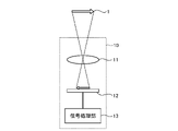
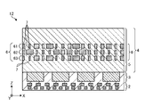
- FIG. 1 is a diagram showing an example of a schematic configuration of an imaging element and an imaging apparatus using an optical element according to an embodiment.
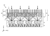
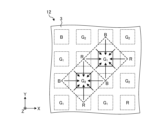
- FIG. 2 is a diagram showing an example of a schematic configuration of an imaging device.
- FIG. 3 is a diagram showing an example of a schematic configuration of an imaging device.
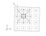
- FIG. 4 is a diagram showing an example of a schematic configuration of an imaging device.
- FIG. 5 is a diagram schematically showing how light is collected on corresponding pixels.
- FIG. 6 is a diagram schematically showing how light is collected on corresponding pixels.
- FIG. 7 is a diagram schematically showing how light is collected on corresponding pixels.
- FIG. 8 is a diagram showing another example of the layered structure of the imaging device.
- FIG. 9 is a diagram showing another example of the layered structure of the imaging device.
- FIG. 9 is a diagram showing another example of the layered structure of the imaging device.
- FIG. 10 is a diagram showing another example of the layered structure of the imaging element.
- FIG. 11 is a diagram showing another example of the layered structure of the imaging device.
- FIG. 12 is a diagram showing another example of the layered structure of the imaging element.
- FIG. 13 is a diagram illustrating an example of a schematic configuration of a structure;
- FIG. 14 is a diagram illustrating an example of a schematic configuration of a structure;
- FIG. 15 is a diagram illustrating an example of a schematic configuration of a structure;
- FIG. 16 is a diagram illustrating an example of a schematic configuration of a structure;
- FIG. 17 is a diagram illustrating an example of a schematic configuration of a structure;
- FIG. 18 is a diagram illustrating an example of a schematic configuration of a structure;
- FIG. 13 is a diagram illustrating an example of a schematic configuration of a structure
- FIG. 14 is a diagram illustrating an example of a schematic configuration of a structure
- FIG. 15 is a
- FIG. 19 is a diagram illustrating an example of a schematic configuration of a structure
- FIG. 20 is a diagram showing a specific example of a color separation microlens design.
- FIG. 21 is a diagram showing a specific example of a color separation microlens design.
- FIG. 22 is a diagram showing a specific example of a color separation microlens design.
- FIG. 23 is a diagram illustrating an example of a cross-sectional shape of a structure;
- FIG. 24 is a diagram showing an example of a schematic configuration of an imaging device according to a modification.
- FIG. 25 is a diagram showing an example of a schematic configuration of an imaging device according to a modification.
- FIG. 1 is a diagram showing an example of a schematic configuration of an imaging element and an imaging device using an optical element according to an embodiment.
- the image capturing apparatus 10 captures an image of the object 1 by using light from the object 1 (subject) illustrated as an outline arrow as incident light. Incident light enters the imaging device 12 via the lens optical system 11 .
- the signal processing unit 13 processes the electrical signal from the imaging device 12 to generate an image signal.
- FIGS. 2 to 4 are diagrams showing examples of the schematic configuration of the imaging device.
- an XYZ coordinate system is shown.
- the XY plane direction corresponds to the surface direction of a layer such as the transparent layer 5 to be described later.
- plane view indicates viewing in the Z-axis direction (for example, in the Z-axis negative direction).
- ide view refers to viewing in the X-axis direction or the Y-axis direction (for example, the Y-axis negative direction).
- the imaging element 12 includes a wiring layer 2, a pixel layer 3, and an optical element 4.
- the wiring layer 2, the pixel layer 3, and the optical element 4 are provided in this order in the Z-axis positive direction.
- FIG. 2 schematically shows the layout of the pixel layer 3 when viewed from above.
- the pixel layer 3 is a pixel array including a plurality of pixels arranged in the XY plane direction. Each pixel includes a photoelectric conversion element.
- An example of a photoelectric conversion element is a photodiode (PD).
- each pixel corresponds to one of red (R), green (G) and blue (B).
- the wavelength is ⁇ 0
- an example of the wavelength region (wavelength band) of red light is ⁇ 0 >600 nm.
- An example wavelength range for green light is 600 nm ⁇ 0 >500 nm.
- An example wavelength range for blue light is 500 nm ⁇ ⁇ 0 .
- Pixels are referred to as pixel R, pixel G 1 , pixel G 2 and pixel B so that each pixel can be distinguished by color.
- These four pixels R, pixel G 1 , pixel G 2 and pixel B are arranged in a Bayer array to form one pixel unit (color pixel unit).
- FIG. 3 shows an example of a cross section of the imaging element 12 when viewed from the side along line III-III' of FIG.
- FIG. 4 shows an example of a cross section of the imaging element 12 when viewed from the side along line IV-IV' of FIG.
- arrows schematically indicate light incident on the imaging device 12 . The incident light travels along the negative direction of the Z-axis and reaches the pixel layer 3 via the optical element 4 .
- the optical element 4 has a color filter function.
- the color filter function is a function of separating incident light into light of each color (each wavelength region).
- the color filter function can also be called a color separation function, a spectral function, a light separation function, or the like.
- the optical element 4 guides the red light to the pixel R, the green light to the pixel G1 and the pixel G2 , and the blue light to the pixel B, among the incident light.
- the incident light most of the light with ⁇ 0 ⁇ 600 nm is guided to the pixel R.
- Most of the light with 500 nm ⁇ 0 ⁇ 600 nm is directed to pixel G 1 and pixel G 2 .
- Most of the light with ⁇ 0 ⁇ 500 nm is directed to pixel B.
- the optical element 4 may also have a lens function.
- a lens function is a function of condensing light of each color onto a corresponding pixel. In this example, red light is focused on the pixel R by the lens function. Green light is focused on pixel G1 and pixel G2 . Blue light is focused on pixel B.
- the optical element 4 has both a color filter function and a lens function.
- Such an optical element 4 can also be called a color separation microlens or the like.
- pixel R In the pixel R, pixel G 1 , pixel G 2 and pixel B, charges are generated according to the amount of received light.
- the charge is converted into an electrical signal that is the basis of the pixel signal by a transistor or the like (not shown) and output to the outside of the imaging device 12 via the wiring layer 2 .
- a transistor or the like not shown
- Some of the wirings included in the wiring layer 2 are illustrated.
- the optical element 4 is provided so as to cover the pixel layer 3 .
- An example of the optical element 4 is a metasurface, which includes a plurality of structures 7 having a width equal to or less than the wavelength of light. By simply changing the parameters of the structure 7, the phase and light intensity can be controlled according to the light characteristics (wavelength, polarization, incident angle, etc.). Details of the structure 7 will be described later.
- FIG. 5 to 7 are diagrams schematically showing how light is collected on corresponding pixels.
- Blue light is focused on the pixel B as indicated by the arrow in FIG.
- FIG. A plurality of structures 7, which will be described later, are arranged so that light of a color corresponding to the pixel B among the light incident outside the region facing the pixel B is also condensed on the pixel B.
- FIG. This makes it possible to increase the amount of received light compared to the case where only the light incident on the region facing the pixel B is condensed on the pixel B.
- Green light is focused on pixel G1 and pixel G2 , as indicated by the arrows in FIG.
- pixels G1 and G2 not only the light above pixels G1 and G2 , but also the light above the pixels surrounding pixels G1 and G2 is focused on pixels G1 and G2 .
- Red light is focused on the pixel R as indicated by the arrow in FIG.
- the pixel R not only the light above the pixel R, but also the light above the pixels surrounding the pixel R are focused on the pixel R.
- a plurality of structures 7, which will be described later, are arranged so that light of a color corresponding to the pixel R among the light incident outside the region facing the pixel R is also condensed on the pixel R.
- FIG. This makes it possible to increase the amount of received light as compared with the case where only the light incident on the region facing the pixel R is condensed on the pixel R.
- the optical element 4 includes a transparent layer 5 and a structure layer 6 in which a plurality of structures 7 are arranged.
- the refractive index of the transparent layer 5 is referred to as refractive index n0 .
- the refractive index of structure 7 is referred to as refractive index n1 .
- the transparent layer 5 is a layer for covering the pixel layer 3 and is provided on the pixel layer 3 .
- the refractive index n 0 of the transparent layer 5 is lower than the refractive index n 1 of the structure 7 .
- An example of the material of the transparent layer 5 is SiO 2 (refractive index 1.45) or the like, in which case the transparent layer 5 may be a SiO 2 substrate or the like.
- the transparent layer 5 may be an air layer, in which case the refractive index of the transparent layer 5 may be equal to that of air.
- the material of the transparent layer 5 may be a single material, or may be a layered material composed of a plurality of materials.
- Each of the plurality of structural bodies 7 arranged in the structural body layer 6 is a nano-order size fine structure having a dimension equal to or smaller than the wavelength of incident light, and is, for example, a columnar structure.
- the refractive index n 1 of the structure 7 is higher than the refractive index n 0 of the transparent layer 5 .
- the plurality of structures 7 are arranged on the opposite side of the pixel layer 3 with at least part of the transparent layer 5 interposed therebetween.
- the plurality of structural bodies 7 are arranged in the plane direction (XY plane) of the transparent layer 5 and the structural layer 6 so as to condense the light of the color corresponding to each of the plurality of pixels among the incident light to the corresponding pixels. direction).
- multiple structures 7 are arranged in multiple layers.
- the plurality of structures 7 are arranged, for example, periodically (having a periodic structure) in the planar direction of the layer.
- the arrangement may be equally spaced for ease of design or may be unevenly spaced.
- the material of each structure 7 may be the same or different from layer to layer.
- the multiple structures 7 are arranged in two layers, a layer 61 (first layer) and a layer 62 (second layer).
- the layers 61 and 62 are layers adjacent to each other in the stacking direction (Z-axis direction).
- the layer 61 is provided on the transparent layer 5 on the opposite side of the transparent layer 5 from the pixel layer 3 .
- a plurality of structures 7 arranged in layer 61 are supported by transparent layer 5 . Above the transparent layer 5 these structures 7 are exposed to air, for example.
- a layer 62 is provided within the transparent layer 5 .
- a plurality of structures 7 arranged in layer 62 are embedded in transparent layer 5 .
- the plurality of structures 7 are arranged in multiple layers so that the structures 7 of each layer are aligned in the stacking direction (Z-axis direction).
- the number of structures 7 arranged in each layer 61 and layer 62 (in each layer) may be the same.
- the structures 7 arranged on the layer 61 and the structures 7 arranged on the layer 62 are arranged in the Z-axis direction. At least a part of these structures 7 overlap when viewed from above.
- an optical phase delay amount ⁇ which will be described later, can be given to the light.
- light incident on a certain structure 7 in the layer 61 and propagating through the structure 7 enters the structure 7 in the layer 62 that at least partially overlaps with the structure 7 when viewed from above. However, it also propagates inside the structure 7 .
- the structures 7 arranged in the stacking direction may be spaced apart from each other. In that case, the separation distance may be equal to or less than the wavelength of the incident light (including approximately the same).
- the wavelength here is the shortest wavelength in the wavelength region of the object of light reception, and is 410 nm, for example. Multiple reflection between layers, dissipation of light after passing through the layers, radiation, etc. are suppressed.
- the thickness (length in the Z-axis direction) of the structure 7 when viewed from the side is referred to as the height of the structure 7.
- Each of the plurality of structures 7 arranged in multiple layers may have a height capable of giving an optical phase delay amount ⁇ of 2 ⁇ or more to light propagating in each of the structures 7 arranged in the stacking direction. This makes it easier to achieve a desired optical phase delay amount distribution, which will be described later with reference to FIGS. 20 to 22, for example.
- a plurality of structures 7 may have the same height at least for each layer.
- each structure 7 arranged in layer 61 may all have the same height.
- Each structure 7 arranged in layer 62 may all have the same height. There are merits such as simplification of design. All structures 7 arranged in each layer may have the same height. By aligning the heights of all the structures 7, the height of each of the plurality of structures 7 can be suppressed as a whole.
- the laminated structure of the imaging device 12 is not limited to the examples shown in FIGS. Some examples of other laminated structures will be described with reference to FIGS. 8-12.
- the structure layer 6 has a three-layer structure further including a layer 63 (third layer).
- the layer 63 is provided on the side opposite to the layer 61 with the layer 62 interposed therebetween.
- a layer configuration of four or more layers may be employed.
- the structural layer 6 is provided within the transparent layer 5.
- each structure 7 arranged in layers 61 and 62 is embedded in the transparent layer 5 .
- the structures 7 arranged in layers 61 , 62 and 63 are all embedded in the transparent layer 5 .
- the transparent layer 5 has a multilayer structure including a transparent substrate 5a and an air layer 5b.
- the air layer 5b is provided between the pixel layer 3 and the transparent substrate 5a.
- Each structure 7 arranged on the layer 61 (first layer) is supported by the transparent substrate 5a. These structures 7 extend into the air layer 5b with the transparent substrate 5a as the proximal end.
- Each structure 7 arranged in another layer is embedded in the transparent substrate 5a.
- each structural body 7 arranged in the layer 62 is embedded in the transparent substrate 5a.
- each structure 7 arranged in the layer 62 and the layer 63 is embedded in the transparent substrate 5a.
- the imaging device 12 may also have various known configurations such as an on-chip microlens, an internal microlens, and a barrier between pixels for reducing crosstalk (not shown).
- the types and dimensions of the cross-sectional shape of each of the plurality of structures 7 when viewed in plan may be the same or different for each layer.
- the types of cross-sectional shapes and dimensions of the structures 7 arranged in the layer 61 may be the same.
- the cross-sectional shape type and dimensions of each structure 7 arranged in the layer 62 may be the same. All the structures 7 arranged on the layers 61 and 62 may have the same cross-sectional shape and dimensions. In the following, a case where structures 7 having different types of cross-sectional shapes and different dimensions are present will be described as an example.
- FIG. 13 to 19 are diagrams showing examples of schematic configurations of structures.
- FIG. 13 schematically shows an example of cross-sectional shapes of a plurality of structures 7 corresponding to the portion surrounded by dashed line XIII in FIG.
- the structures 7 having different types of cross-sectional shapes are shown as structures 71, 72, and 73 so as to be distinguished from each other.
- 14 and 15 show examples of the schematic configuration of the structure 71 when viewed from the side and from the top.
- 16 and 17 show examples of the schematic configuration of the structure 72 when viewed from the side and from the top.
- 18 and 19 show examples of the schematic configuration of the structure 73 when viewed from the side and from the top.
- the height of the structure 7 in each layer is referred to as height h layer and is illustrated.
- the cross-sectional shape of the illustrated structural body 7 is all four-fold rotationally symmetrical shapes.
- the 4-fold rotationally symmetric shape includes, for example, at least one of a square shape, a cross shape, and a circular shape.
- the cross-sectional shape of the structure 71 is square.
- the cross-sectional shape of the structure 72 is X-shaped.
- the X shape is an example of a shape including a cross shape, and is a shape obtained by rotating the cross shape by 45° in-plane.
- the cross-sectional shape of the structure 73 is a hollow diamond shape.
- a hollow rhombus shape is an example of a shape including a square shape, and is a shape obtained by in-plane rotation of a hollow square shape having square holes by 45°.
- the width of the portion of the transparent layer 5 surrounding (including inside) each structure 7 in the XY plane direction is referred to as a width W and illustrated.
- the width W gives the arrangement period of the structures 7 .
- the width W may be set to W ⁇ ( ⁇ min /n 0 ) so that no diffracted light occurs on the transmission side.
- ⁇ min is the shortest wavelength in the wavelength range to be received, for example 410 nm.
- a plurality of structures 7 having various types of cross-sectional shapes and dimensions as described above are arranged in the XY plane direction as shown in FIG. 13, for example.
- the Bayer array As can be understood from the comparison with FIG . It has an overall arrangement structure obtained by rotating the overall arrangement structure of the plurality of structures 7 arranged in the region facing the pixel G 1 ) by 90°. This is because the pixel G1 and the pixel G2 have different arrangements of the adjacent pixels R and B, respectively.
- the structure 7 behaves as an optical waveguide that confines and propagates light within the structure.
- the structure 7 gives a phase delay amount to the light that has entered the structure 7 and propagated through the structure 7 .
- a phase delay amount provided by the structure 7 of each layer is referred to as an optical phase delay amount ⁇ layer .
- the end surface of the structure 7 on the Z-axis positive direction side is called the top surface
- the end surface of the structure 7 on the Z-axis negative direction side is called the bottom surface.
- the effective refractive index n eff is known to greatly depend on the cross-sectional shape of the structure 7 and is higher than the refractive index n 0 and lower than the refractive index n 1 (n 0 ⁇ n eff ⁇ n 1 ).
- the effective refractive index n eff also varies depending on the wavelength ⁇ , and the degree of variation also largely depends on the cross-sectional shape of the structure 7 .
- the optical phase delay amount ⁇ layer has chromatic dispersion characteristics.
- a plurality of structures 7 can be arranged so as to provide different optical wavefronts for each wavelength region by utilizing the chromatic dispersion characteristics. For example, by using the structure 7 having various cross-sectional shapes as described above with reference to FIG. 13, it is possible to design various combinations of the optical phase delay amount ⁇ layer according to the wavelength ⁇ of light. . A variety of color-separating microlenses with different focal positions depending on the wavelength range can be realized.
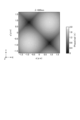
- FIG. 20 to 22 are diagrams showing specific examples of color separation microlens design.
- FIG. 20 shows an ideal optical phase delay amount distribution when the center wavelength is 430 nm (blue light).
- FIG. 21 shows an ideal optical phase delay amount distribution when the center wavelength is 520 nm (green light).
- FIG. 22 shows an ideal optical phase delay amount distribution when the center wavelength is 635 nm (red light).
- the pixel size is 1.68 ⁇ m ⁇ 1.68 ⁇ m.
- the focal length is 4.2 ⁇ m.
- the central wavelength corresponding to blue light is 430 nm.
- the central wavelength corresponding to green light is 520 nm.
- the central wavelength corresponding to red light is 635 m.
- Equation (2) ⁇ d is the center wavelength (design wavelength).
- x f , y f and z f are the focal positions.
- n2 is the refractive index of the lower transparent layer 5; C is an arbitrary constant.
- the optical phase delay amount ⁇ is converted so that it falls within the range of 0 to 2 ⁇ . For example, -0.5 ⁇ and 2.5 ⁇ are converted to 1.5 ⁇ and 0.5 ⁇ respectively.
- the boundary region of the optical phase delay amount distribution was set so that the optical phase delay amount distribution at each center wavelength was horizontally and vertically symmetrical (together with adjacent lenses) with respect to the condensing position.
- the constant C may be optimized so that the error (difference from the ideal value) in the optical phase delay amount distribution is minimized at each wavelength.
- a plurality of structures 7 are arranged in multiple layers so that the optical phase delay amount distributions shown in FIGS. 20 to 22 are obtained.
- the total sum of the optical phase delay amounts ⁇ layer given by the structures 7 arranged in the stacking direction gives the optical phase delay amount ⁇ at that position.
- each of the plurality of structures 7 arranged in multiple layers has a height that can give an optical phase delay amount ⁇ of 2 ⁇ or more to the light propagating in each of the structures 7 arranged in the stacking direction. By having it, it is possible to correspond to a desired optical phase delay amount distribution.
- the structure 7 that best matches the optical phase delay amount distribution at each center wavelength is arranged at the corresponding position.
- the height h layer of each of the plurality of structures 7 is given by, for example, formula (3) below.
- ⁇ r is the desired central wavelength in the wavelength region on the longest wavelength side of the wavelength regions of light to be color-separated.
- L is the number of layers. What is important is that the height h layer can be reduced by the number of layers as compared to the single layer arrangement. For example, even if a single-layer arrangement requires a height of 1200 nm, a two-layer arrangement can reduce the required height to half, ie, 600 nm.
- the value of the effective refractive index neff and wavelength dispersion can be changed for each layer. Since the optical phase delay amount ⁇ is the sum of the optical phase delay amounts ⁇ layer of each layer, various combinations of the optical phase delay amounts ⁇ layer of each layer can increase the degree of freedom in design. Design parameters are increased by the number of layers, light controllability is improved, and a more efficient color separation function can be obtained. High-contrast color separation and reduction of color crosstalk are also possible.
- the optical element 4 realizes a color separation function and a lens function by arranging a plurality of structures 7 in multiple layers.
- a filter color filter or the like
- the filter absorbs light of wavelengths other than the transmission wavelength range, so the amount of light after passing through the filter is, for example, 1 of the amount of light incident on the filter. /3 remains, and the light receiving efficiency decreases.
- the amount of light after transmission is considerably larger than that (for example, 90% or more), and the light receiving efficiency and sensitivity are greatly improved.
- a structure is also known in which a microlens is provided (integrated) on the opposite side of a pixel with a filter interposed therebetween. Manufacturing costs also increase. By realizing the color separation function and the lens function only with the optical element 4, the configuration can be simplified and the manufacturing cost can be reduced. In addition, since the plurality of structures 7 can be arranged within the plane (in the XY plane) without gaps, the aperture ratio is increased.
- the height h layer of the structures 7 in each layer can be reduced compared to the case of single layer arrangement as in Non-Patent Document 1, for example.
- the height h layer should be ⁇ r /(n 1 ⁇ n 0 ) or more.
- the dimensions of the actual cross-sectional shape of the structure 7 are designed to be smaller than the period described above for the purpose of reducing optical coupling with adjacent structures 7 . Assuming a maximum cross-sectional dimension of 200 nm, the aspect ratio is about 5.3 or greater. Additionally, smaller dimensions may be used to control the effective refractive index n eff , with a minimum dimension of 80 nm, resulting in an aspect ratio of about 13.3 or greater.
- the height of the entire structure 7 is shared (divided) by the structure 7 of each layer, and the height h layer of the structure 7 in each layer is It can be reduced more than in the case of a single layer arrangement. As a result, the aspect ratio of structure 7 can be reduced.
- the materials of the transparent layer 5 and the structure 7 are SiO 2 and SiN, and the number of layers L is a two-layer structure. 530 nm or more, which is about 1/2, is sufficient.
- the aspect ratio can be reduced to about 1/2.
- the aspect ratio can be reduced to about 1/3.
- the signal processing unit 13 of the imaging device 10 will be described.
- the signal processing unit 13 generates pixel signals based on the electrical signals obtained from the imaging device 12 .
- the signal processing unit 13 also controls the imaging element 12 to obtain the electrical signal.
- the control of the imaging device 12 includes exposing pixels of the imaging device 12, converting electric charges accumulated in the pixel layer 3 into electric signals, reading electric signals, and the like.
- FIG. 23 is a diagram illustrating an example of a cross-sectional shape of a structure; Structure 7 may have various cross-sectional shapes as illustrated. Exemplified shapes are four-fold rotationally symmetrical shapes obtained by various combinations of square shapes, cross shapes, circular shapes, and the like.
- the imaging device may have a filter.
- 24 and 25 are diagrams showing an example of a schematic configuration of an imaging device according to such a modification.
- the illustrated image sensor 12A includes a filter layer 8 provided between the pixel layer 3 and the optical element 4 (the transparent layer 5 thereof).
- FIG. 24 shows an example of a cross section of the image sensor 12A when viewed from the side along the line III-III' when the image sensor 12 in FIG. 2 is replaced with the image sensor 12A.
- FIG. 25 shows an example of a cross-section of the image sensor 12A when viewed from the side along line IV-IV' when the image sensor 12 in FIG. 2 is replaced with the image sensor 12A.
- the filter layer 8 includes a filter 8R, a filter 8G1 , a filter 8G2 and a filter 8B.
- the filter 8R is provided so as to cover the pixel R and allows red light to pass therethrough.
- a filter 8G1 is provided to cover the pixel G1 and allows green light to pass therethrough.
- a filter 8G2 is provided to cover the pixel G2 and allows green light to pass therethrough.
- the filter 8B is provided so as to cover the pixel B and allows blue light to pass therethrough.
- Examples of materials for the filters 8R, 8G 1 , 8G 2 and 8B are organic materials such as resin.
- the light color-separated by the optical element 4 further passes through the filter layer 8 and then reaches the pixel layer 3 .
- the color separation of both the optical element 4 and the filter layer 8 results in less spectral cross-talk (removing most of the unwanted other color components) and better color reproduction than if only one was color separated. improves.
- the amount of light is not greatly reduced. Therefore, compared with the case where only the filter layer 8 is provided without the optical element 4, the light receiving efficiency of the pixel is improved.
- the imaging element 12A including the filter layer 8 it is possible to improve the light receiving efficiency and further improve the color reproducibility.
- SiN and TiO 2 are used as examples of the material of the structure 7 .
- the material of the structure 7 is not limited to them.
- SiN, SiC, TiO 2 , GaN, or the like may be used as the material of the structure 7 . It is suitable because of its high refractive index and low absorption loss.
- Si, SiC, SiN, TiO 2 , GaAs, GaN, or the like may be used as the material of the structure 7 .
- InP or the like can be used as the material of the structure 7 in addition to the materials described above for light in the long-wavelength near-infrared region (communication wavelengths of 1.3 ⁇ m, 1.55 ⁇ m, etc.).
- polyimide such as fluorinated polyimide, BCB (benzocyclobutene), photocurable resin, UV epoxy resin, acrylic resin such as PMMA, and polymer such as resist in general. etc. are mentioned as materials.
- the material of the transparent layer 5 is not limited to these. Any material having a lower refractive index than the material of the structure 7 and a low loss with respect to the wavelength of the incident light may be used, including general glass materials.
- the transparent layer 5 may be made of the same material as the color filter, or may be made of an organic material such as resin, as long as the loss is sufficiently low with respect to the wavelength of light that should reach the corresponding pixel. good. In this case, the transparent layer 5 is not only made of the same material as the color filter, but also has the same structure as the color filter and is designed to have absorption characteristics according to the wavelength of light to be guided to the corresponding pixel. may
- structures 71, 72, and 73 are used as the structure 7 .
- one type of structure for example, structure 71, structure 72, or structure 73
- four or more types of structures may be used.
- the optical element 4 is for covering a plurality of pixels (for example, pixel R, pixel G 1 , pixel G 2 and pixel B) each including a photoelectric conversion element.
- the plurality of structures 7 are arranged in multiple layers so as to guide light of colors corresponding to each of the plurality of pixels among the incident light to the corresponding pixels.
- the optical element 4 described above achieves a color separation function by means of a plurality of structures 7 arranged in multiple layers. As a result, the aspect ratio of the structure 7 in each layer can be reduced, and the difficulty of manufacturing the structure 7 can be lowered as compared with the single-layer arrangement.
- each of the plurality of structures 7 has a refractive index n1 higher than the refractive index n0 of the transparent layer 5, and the light propagating through the structures 7 is a columnar structure that provides an optical phase delay amount ⁇ layer for .
- each of the plurality of structures 7 may have a height h layer capable of giving an optical phase delay amount ⁇ of 2 ⁇ or more to light propagating in each of the structures 7 arranged in the stacking direction (Z-axis direction). .
- Z-axis direction Z-axis direction
- the plurality of structures 7 may be arranged in multiple layers according to the optical phase amount delay distribution for condensing light of corresponding colors onto corresponding pixels. Thereby, a lens function can also be realized.
- a plurality of structures 7 arranged in multiple layers can be used as color separation microlenses.
- the configuration can be simplified and the manufacturing cost can be reduced as compared with the case of adopting a two-layer configuration of color separation filters and microlenses.
- the plurality of structures 7 can be arranged within the plane (in the XY plane) without gaps, the aperture ratio is increased.
- the plurality of structures 7 may have the same height h layer at least for each layer. There are merits such as simplification of design. When all structures 7 have the same height h layer , the height of each of the plurality of structures 7 can be suppressed as a whole.
- the plurality of structures 7 are arranged in multiple layers so that the structures of each layer are aligned in the stacking direction (Z-axis direction), and arranged in each layer.
- the number of structures 7 may be the same.
- a light phase delay amount ⁇ can be given by propagating light through each of the structures 7 arranged in the layer direction.
- all of the plurality of structures 7 may be embedded in the transparent layer 5.
- FIG. Color separation and microlens design based on the refractive index n0 of the transparent layer 5 are possible, and the design is facilitated.
- the imaging device 12 and the imaging device 10 described with reference to FIGS. 1 to 4 are also one of disclosed techniques.
- the imaging device 12 includes an optical element 4 and a plurality of pixels covered with a transparent layer 5.
- the imaging device 10 includes an imaging device 12 and a signal processing unit 13 that generates an image signal based on an electrical signal obtained from the imaging device 12 .
Landscapes
- Physics & Mathematics (AREA)
- General Physics & Mathematics (AREA)
- Optics & Photonics (AREA)
- Solid State Image Pick-Up Elements (AREA)
Priority Applications (4)
| Application Number | Priority Date | Filing Date | Title |
|---|---|---|---|
| PCT/JP2021/030262 WO2023021632A1 (ja) | 2021-08-18 | 2021-08-18 | 光学素子、撮像素子及び撮像装置 |
| US18/683,149 US12364042B2 (en) | 2021-08-18 | 2021-08-18 | Optical element having both color filter function and lens function, image sensor thereof and imaging device |
| JP2023542110A JPWO2023021632A1 (https=) | 2021-08-18 | 2021-08-18 | |
| US19/246,219 US20250366235A1 (en) | 2021-08-18 | 2025-06-23 | Optical element, image sensor and imaging device |
Applications Claiming Priority (1)
| Application Number | Priority Date | Filing Date | Title |
|---|---|---|---|
| PCT/JP2021/030262 WO2023021632A1 (ja) | 2021-08-18 | 2021-08-18 | 光学素子、撮像素子及び撮像装置 |
Related Child Applications (2)
| Application Number | Title | Priority Date | Filing Date |
|---|---|---|---|
| US18/683,149 A-371-Of-International US12364042B2 (en) | 2021-08-18 | 2021-08-18 | Optical element having both color filter function and lens function, image sensor thereof and imaging device |
| US19/246,219 Continuation US20250366235A1 (en) | 2021-08-18 | 2025-06-23 | Optical element, image sensor and imaging device |
Publications (1)
| Publication Number | Publication Date |
|---|---|
| WO2023021632A1 true WO2023021632A1 (ja) | 2023-02-23 |
Family
ID=85240259
Family Applications (1)
| Application Number | Title | Priority Date | Filing Date |
|---|---|---|---|
| PCT/JP2021/030262 Ceased WO2023021632A1 (ja) | 2021-08-18 | 2021-08-18 | 光学素子、撮像素子及び撮像装置 |
Country Status (3)
| Country | Link |
|---|---|
| US (2) | US12364042B2 (https=) |
| JP (1) | JPWO2023021632A1 (https=) |
| WO (1) | WO2023021632A1 (https=) |
Citations (4)
| Publication number | Priority date | Publication date | Assignee | Title |
|---|---|---|---|---|
| JP2015028960A (ja) * | 2011-12-01 | 2015-02-12 | ソニー株式会社 | 固体撮像装置および電子機器 |
| US20160260762A1 (en) * | 2015-03-02 | 2016-09-08 | Samsung Electronics Co., Ltd. | Image sensor including color filter and method of manufacturing the image sensor |
| JP2021069118A (ja) * | 2019-10-23 | 2021-04-30 | 三星電子株式会社Samsung Electronics Co.,Ltd. | 色分離レンズアレイを具備するイメージセンサ、及びそれを含む電子装置 |
| JP2021069119A (ja) * | 2019-10-23 | 2021-04-30 | 三星電子株式会社Samsung Electronics Co.,Ltd. | 色分離レンズアレイを具備するイメージセンサ、及びそれを含む電子装置 |
Family Cites Families (6)
| Publication number | Priority date | Publication date | Assignee | Title |
|---|---|---|---|---|
| JP2009252978A (ja) * | 2008-04-04 | 2009-10-29 | Panasonic Corp | 固体撮像素子およびその製造方法 |
| JP2012064703A (ja) * | 2010-09-15 | 2012-03-29 | Sony Corp | 撮像素子および撮像装置 |
| JP6356557B2 (ja) * | 2013-09-30 | 2018-07-11 | 株式会社豊田中央研究所 | レンズおよびその製造方法 |
| US10790325B2 (en) * | 2015-07-29 | 2020-09-29 | Samsung Electronics Co., Ltd. | Imaging apparatus and image sensor including the same |
| US11711600B2 (en) * | 2019-07-09 | 2023-07-25 | Samsung Electronics Co., Ltd. | Meta-optical device and optical apparatus including the same |
| CN113257846A (zh) * | 2020-02-11 | 2021-08-13 | 三星电子株式会社 | 图像传感器和包括图像传感器的电子设备 |
-
2021
- 2021-08-18 WO PCT/JP2021/030262 patent/WO2023021632A1/ja not_active Ceased
- 2021-08-18 JP JP2023542110A patent/JPWO2023021632A1/ja active Pending
- 2021-08-18 US US18/683,149 patent/US12364042B2/en active Active
-
2025
- 2025-06-23 US US19/246,219 patent/US20250366235A1/en active Pending
Patent Citations (4)
| Publication number | Priority date | Publication date | Assignee | Title |
|---|---|---|---|---|
| JP2015028960A (ja) * | 2011-12-01 | 2015-02-12 | ソニー株式会社 | 固体撮像装置および電子機器 |
| US20160260762A1 (en) * | 2015-03-02 | 2016-09-08 | Samsung Electronics Co., Ltd. | Image sensor including color filter and method of manufacturing the image sensor |
| JP2021069118A (ja) * | 2019-10-23 | 2021-04-30 | 三星電子株式会社Samsung Electronics Co.,Ltd. | 色分離レンズアレイを具備するイメージセンサ、及びそれを含む電子装置 |
| JP2021069119A (ja) * | 2019-10-23 | 2021-04-30 | 三星電子株式会社Samsung Electronics Co.,Ltd. | 色分離レンズアレイを具備するイメージセンサ、及びそれを含む電子装置 |
Also Published As
| Publication number | Publication date |
|---|---|
| US12364042B2 (en) | 2025-07-15 |
| JPWO2023021632A1 (https=) | 2023-02-23 |
| US20250366235A1 (en) | 2025-11-27 |
| US20240347566A1 (en) | 2024-10-17 |
Similar Documents
| Publication | Publication Date | Title |
|---|---|---|
| JP7364066B2 (ja) | 撮像素子及び撮像装置 | |
| JP7574860B2 (ja) | 撮像素子及び撮像装置 | |
| KR20200099832A (ko) | 다층 메타 렌즈 및 이를 포함하는 광학 장치 | |
| KR20200029572A (ko) | 컬러촬상소자 및 촬상장치 | |
| JP7574859B2 (ja) | 撮像素子及び撮像装置 | |
| JP7773081B2 (ja) | 分光素子アレイ、撮像素子および撮像装置 | |
| KR102831769B1 (ko) | 광학 소자, 촬상 소자 및 촬상장치 | |
| US20120001285A1 (en) | Solid state imaging apparatus | |
| JP7563473B2 (ja) | 撮像素子及び撮像装置 | |
| JP7231869B2 (ja) | 撮像素子および撮像装置 | |
| JP7635787B2 (ja) | 光学素子、撮像素子及び撮像装置 | |
| WO2023021632A1 (ja) | 光学素子、撮像素子及び撮像装置 | |
| JP7563471B2 (ja) | 撮像素子及び撮像装置 | |
| US12622079B2 (en) | Optical element, image sensor and imaging device for wavwlength-dependent focusing of visible and near-infrared light | |
| JP2025010437A (ja) | カラー撮像素子および撮像装置 | |
| WO2025258002A1 (ja) | 撮像素子および撮像装置 |
Legal Events
| Date | Code | Title | Description |
|---|---|---|---|
| 121 | Ep: the epo has been informed by wipo that ep was designated in this application |
Ref document number: 21954205 Country of ref document: EP Kind code of ref document: A1 |
|
| WWE | Wipo information: entry into national phase |
Ref document number: 2023542110 Country of ref document: JP |
|
| WWE | Wipo information: entry into national phase |
Ref document number: 18683149 Country of ref document: US |
|
| NENP | Non-entry into the national phase |
Ref country code: DE |
|
| 122 | Ep: pct application non-entry in european phase |
Ref document number: 21954205 Country of ref document: EP Kind code of ref document: A1 |
|
| WWG | Wipo information: grant in national office |
Ref document number: 18683149 Country of ref document: US |