WO2023013349A1 - Module optique et câble de connecteur optique - Google Patents
Module optique et câble de connecteur optique Download PDFInfo
- Publication number
- WO2023013349A1 WO2023013349A1 PCT/JP2022/026759 JP2022026759W WO2023013349A1 WO 2023013349 A1 WO2023013349 A1 WO 2023013349A1 JP 2022026759 W JP2022026759 W JP 2022026759W WO 2023013349 A1 WO2023013349 A1 WO 2023013349A1
- Authority
- WO
- WIPO (PCT)
- Prior art keywords
- lens
- optical
- substrate
- module
- cavity
- Prior art date
Links
- 230000003287 optical effect Effects 0.000 title claims abstract description 256
- 239000000758 substrate Substances 0.000 claims abstract description 142
- 239000013307 optical fiber Substances 0.000 claims abstract description 90
- 239000000853 adhesive Substances 0.000 claims abstract description 80
- 230000001070 adhesive effect Effects 0.000 claims abstract description 80
- 230000002265 prevention Effects 0.000 claims abstract description 46
- 239000000835 fiber Substances 0.000 claims description 3
- 230000008878 coupling Effects 0.000 description 19
- 238000010168 coupling process Methods 0.000 description 19
- 238000005859 coupling reaction Methods 0.000 description 19
- 230000004048 modification Effects 0.000 description 14
- 238000012986 modification Methods 0.000 description 14
- 238000010586 diagram Methods 0.000 description 6
- 239000000463 material Substances 0.000 description 6
- 230000001681 protective effect Effects 0.000 description 6
- 239000011347 resin Substances 0.000 description 4
- 229920005989 resin Polymers 0.000 description 4
- 238000005452 bending Methods 0.000 description 2
- 238000006243 chemical reaction Methods 0.000 description 2
- 239000011521 glass Substances 0.000 description 2
- 230000007246 mechanism Effects 0.000 description 2
- 239000002184 metal Substances 0.000 description 2
- 230000000630 rising effect Effects 0.000 description 2
- 230000000903 blocking effect Effects 0.000 description 1
- 230000008859 change Effects 0.000 description 1
- 239000003795 chemical substances by application Substances 0.000 description 1
- 239000011248 coating agent Substances 0.000 description 1
- 238000000576 coating method Methods 0.000 description 1
- 230000007423 decrease Effects 0.000 description 1
- 230000000694 effects Effects 0.000 description 1
- 239000003365 glass fiber Substances 0.000 description 1
- 230000000149 penetrating effect Effects 0.000 description 1
- 230000001902 propagating effect Effects 0.000 description 1
- 230000035939 shock Effects 0.000 description 1
Images


Classifications
-
- G—PHYSICS
- G02—OPTICS
- G02B—OPTICAL ELEMENTS, SYSTEMS OR APPARATUS
- G02B6/00—Light guides; Structural details of arrangements comprising light guides and other optical elements, e.g. couplings
- G02B6/24—Coupling light guides
- G02B6/26—Optical coupling means
- G02B6/32—Optical coupling means having lens focusing means positioned between opposed fibre ends
-
- G—PHYSICS
- G02—OPTICS
- G02B—OPTICAL ELEMENTS, SYSTEMS OR APPARATUS
- G02B6/00—Light guides; Structural details of arrangements comprising light guides and other optical elements, e.g. couplings
- G02B6/24—Coupling light guides
- G02B6/42—Coupling light guides with opto-electronic elements
-
- H—ELECTRICITY
- H01—ELECTRIC ELEMENTS
- H01S—DEVICES USING THE PROCESS OF LIGHT AMPLIFICATION BY STIMULATED EMISSION OF RADIATION [LASER] TO AMPLIFY OR GENERATE LIGHT; DEVICES USING STIMULATED EMISSION OF ELECTROMAGNETIC RADIATION IN WAVE RANGES OTHER THAN OPTICAL
- H01S5/00—Semiconductor lasers
- H01S5/02—Structural details or components not essential to laser action
- H01S5/022—Mountings; Housings
- H01S5/0225—Out-coupling of light
- H01S5/02253—Out-coupling of light using lenses
Definitions
- the present disclosure relates to optical modules and optical connector cables.
- This application claims priority based on Japanese Application No. 2021-128962 filed on August 5, 2021, and incorporates all the descriptions described in the Japanese Application.
- Patent Document 1 discloses an example of an optical component (optical module) that optically connects an optical fiber to a photoelectric conversion element (optical element) mounted on a substrate.
- This optical component converts the light emitted horizontally from the optical fiber into light propagating in the vertical direction by means of the lens component, and makes this light incident on the photoelectric conversion element mounted on the substrate.
- the optical module of the present disclosure includes a substrate, an optical element, and a lens module.
- the optical element is mounted on the substrate.
- the lens module has an outer surface and an inner surface facing each other, and a lens provided on the inner surface so as to be optically coupled to the optical element, and optically couples the optical fiber and the optical element via the lens.
- the lens module is mounted on the substrate so that the inner surface faces the substrate, and is attached to the substrate by an adhesive introduced into the gap between the inner surface and the substrate.
- An inflow prevention structure is provided between the substrate and the lens module and between the lens and the adhesive to prevent the adhesive from flowing into the optical axis of the lens.
- An optical connector cable of the present disclosure includes the optical module described above and an optical fiber cable.
- a fiber optic cable has at least one optical fiber.
- the optical fiber cable is attached to the optical module so that the optical fiber is optically coupled to the optical element through the lens.
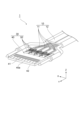
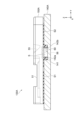
- FIG. 1 is a perspective view showing an optical connector cable according to one embodiment.
- FIG. 2 is a perspective view showing the optical connector cable with the protective member removed.
- FIG. 3 is a plan view of the optical module viewed from above the first surface of the substrate.
- FIG. 4 is a plan view of the optical module viewed from above the second surface of the substrate.
- FIG. 5 is a cross-sectional view of the optical module taken along line VV shown in FIG.
- FIG. 6 is an enlarged view of a portion surrounded by dashed line A shown in FIG. 7 is a perspective view showing a substrate used in the optical module shown in FIG. 3.
- FIG. FIG. 8 is an enlarged view of a portion surrounded by dashed line B shown in FIG.
- FIG. 9 is an enlarged view of a portion surrounded by dashed line C shown in FIG.
- FIG. 10 is a schematic diagram of a partial cross section showing the configuration of an optical module according to the first modified example.
- FIG. 11 is a schematic diagram of a partial cross section showing the configuration of an optical module according to a second modification.
- FIG. 12 is a schematic diagram of a partial cross section showing the configuration of an optical module according to a third modified example.
- FIG. 13A is a plan view showing an example of the inner surface of the lens module used in the third modified example.
- FIG. 13B is a plan view showing another example of the inner surface of the lens module used in the third modified example;
- FIG. 13C is a plan view showing still another example of the inner surface of the lens module used in the third modified example.
- a conventional optical module optically connects an optical fiber and an optical element via a lens provided on the inner surface of the optical module.
- an adhesive is introduced between the substrate and the lens module to fix them together.
- the gap between the substrate and the lens module becomes minute, and it becomes difficult to control the spread of the adhesive introduced into the gap. For this reason, part of the adhesive may flow into the vicinity of the lens provided inside the inner surface of the lens module, blocking the optical path of the lens for optically coupling the optical fiber and the optical element.
- An object of the present disclosure is to provide an optical module and an optical connector cable capable of stably optically coupling an optical fiber and an optical element by preventing obstruction of the lens optical path.
- optical coupling between an optical fiber and an optical element can be stably performed.
- An optical module includes a substrate, an optical element, and a lens module.
- the optical element is mounted on the substrate.
- the lens module has an outer surface and an inner surface facing each other, and a lens provided on the inner surface so as to be optically coupled to the optical element, and optically couples the optical fiber and the optical element via the lens.
- the lens module is mounted on the substrate so that the inner surface faces the substrate, and is attached to the substrate by an adhesive introduced into the gap between the inner surface and the substrate.
- An inflow prevention structure is provided between the substrate and the lens module and between the lens and the adhesive to prevent the adhesive from flowing into the optical axis of the lens.
- an inflow prevention structure is provided between the substrate and the lens module and between the lens and the adhesive to prevent the adhesive from flowing into the optical axis of the lens.
- This inflow prevention structure prevents the adhesive introduced into the gap between the lens module and the substrate from flowing into the lens provided on the inner surface of the lens module, and the lens for optically coupling the optical fiber and the optical element.
- the adhesive does not block the optical path of Therefore, according to this optical module, optical coupling between the optical fiber and the optical element can be stably performed.
- the inflow prevention structure may include a groove or recess provided near the area facing the lens on the surface of the substrate facing the lens module. According to this aspect, it is possible to prevent the adhesive introduced into the gap between the substrate and the lens module from flowing into the optical axis of the lens with a simple configuration. Therefore, according to this optical module, optical coupling between the optical fiber and the optical element can be stably performed with a simple configuration.
- the vicinity of the area referred to here is intended to include not only the area facing the lens but also the area between this facing area and the adhesive.
- the groove or recess which is the inflow prevention structure, may extend along the width direction crossing the longitudinal direction in the plane direction of the substrate, or may extend to the outside in the width direction.
- the inflow prevention structure may include a wall provided between the lens and the adhesive on the inner surface of the lens module. According to this aspect, it is possible to prevent the adhesive introduced into the gap between the substrate and the lens module from flowing into the optical axis of the lens with a simple configuration. Therefore, according to this optical module, optical coupling between the optical fiber and the optical element can be stably performed with a simple configuration.
- the wall which is the inflow prevention structure, may extend along the width direction crossing the longitudinal direction in the surface direction of the lens module, or may extend to the outside in the width direction. The wall may also abut the substrate when the lens module is attached to the substrate with an adhesive. Thereby, the inflow of the adhesive can be prevented more reliably.
- the width of the gap between the substrate and the inner surface of the lens module is 1 mm or less, and the adhesive may be introduced into this gap.
- the substrate and the lens module are mounted thinner, and the optical module can be made thinner. If the adhesive is introduced into such a minute gap, there is a risk that the adhesive will easily reach the interior. The adhesive is prevented from adhering to the optical axis of the optical fiber, and optical coupling between the optical fiber and the optical element can be stably performed.
- the inflow prevention structure may be provided in a region within 5 mm from the optical axis of the lens in the plane direction orthogonal to the optical axis. According to this aspect, it is possible to more reliably attach the lens module to the substrate while ensuring a sufficient amount of adhesive to be introduced between the substrate and the lens module.
- the anti-inflow structure may include a first anti-inflow structure and a second anti-inflow structure, the first anti-inflow structure is arranged on one side with respect to the lens, and the second anti-inflow structure is on the lens. may be arranged on the other side.
- the substrate may be formed with a cavity recessed from the first side of the substrate toward the second side of the substrate to have a bottom, the cavity accommodating at least a portion of the lens module.
- the cavity may have a first cavity and a second cavity having a second bottom located closer to the second surface than the first bottom of the first cavity.
- a lens may be housed in the second cavity.
- the thickness of the optical module can be reduced more reliably.
- the inflow prevention structure may be accommodated in the second cavity.
- the lens module is configured such that light emitted from an optical fiber mounted on the outer surface enters the optical element, or light emitted from the optical element enters the optical fiber mounted on the outer surface. It may have a mirror to change the direction of propagation of the light so that it is incident on the .
- the optical fiber positioned along the substrate and the optical element positioned across the substrate from the optical fiber can be optically coupled using the mirror.
- An optical connector cable includes any one of the optical modules described above and an optical fiber cable.
- a fiber optic cable has at least one optical fiber.
- the optical fiber cable is attached to the optical module so that the optical fiber is optically coupled to the optical element through the lens.
- an inflow prevention structure is provided between the substrate and the lens module and between the lens and the adhesive to prevent the adhesive from flowing into the optical axis of the lens. According to this aspect, it is possible to prevent the adhesive introduced into the gap between the substrate and the lens module from flowing into the lens provided on the inner surface of the lens module. Therefore, according to this optical connector cable, optical coupling between the optical fiber and the optical element can be stably performed.
- FIG. 1 is a perspective view showing an optical connector cable 1 according to one embodiment.
- FIG. 2 is a perspective view showing the optical connector cable 1 with the protective member 20 removed.
- the width direction of the end of the optical connector cable 1 is defined as the direction X
- the extending direction of the end is defined as the direction Y
- the thickness direction of the end is defined as the direction Z.
- direction X, direction Y and direction Z are orthogonal to each other.
- the optical connector cable 1 is a cable used for transmitting and receiving optical signals between devices, for example. As shown in FIGS. 1 and 2, the optical connector cable 1 includes an optical fiber cable 10, a protective member 20, and an optical module 30. FIG. 1 and 2 show one end of the optical fiber cable 10, the other end of the optical fiber cable 10 may have a similar configuration.
- the optical fiber cable 10 has a plurality of optical fibers 11 and a cable jacket 12.
- Each optical fiber 11 is a member for transmitting an optical signal. Most of each optical fiber 11 is housed inside the cable jacket 12 , and the tip portion thereof is exposed to the outside of the cable jacket 12 .
- the plurality of optical fibers 11 are arranged one-dimensionally along the direction X. As shown in FIG. Inside the cable jacket 12, all the optical fibers 11 are housed in close proximity to each other. On the other hand, outside the cable jacket 12 , the plurality of optical fibers 11 are branched into bundles of several (four to six in this embodiment), and the ends of the bundles are held by respective lens modules 50 .
- Each optical fiber 11 may be formed, for example, by coating a glass fiber composed of a core and a clad surrounding the core with a resin.
- Each optical fiber 11 may be a single mode optical fiber (SMF) or a multimode optical fiber (MMF).
- the protection member 20 is a flat member that expands along the direction X and the direction Y, and can accommodate the optical module 30 inside.
- the protective member 20 protects the optical module 30 from external shocks and the like.
- the protective member 20 has a laminated structure consisting of an inner layer 21 and an outer layer 22 covering the inner layer 21 .
- the material of the inner layer 21 may be metal, for example.
- the material of the outer layer 22 may be resin, for example.
- a portion of the inner layer 21 is exposed from the outer layer 22 at the tip of the optical connector cable 1 . This exposed portion is inserted, for example, into a receptacle provided in a device to which the optical connector cable 1 is connected.
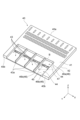
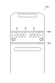
- FIG. 3 is a plan view of the optical module 30 viewed from above the first surface 41 of the substrate 40.
- FIG. 4 is a plan view of the optical module 30 viewed from above the second surface 42 of the substrate 40.
- FIG. FIG. 5 is a cross-sectional view of the optical module 30 taken along line VV shown in FIG.
- FIG. 6 is an enlarged view of a portion surrounded by dashed line A shown in FIG.
- the optical module 30 includes a substrate 40 , multiple lens modules 50 , multiple optical elements 60 , and multiple ICs 61 .
- the substrate 40 is a plate-like member on which various optical elements and electronic elements are mounted.
- the substrate 40 has a first end face 40a and a second end face 40b facing each other in the direction Y, and may be a thin substrate having a thickness of 0.2 mm or more and 0.8 mm or less, for example.
- Various wirings (not shown) for electrically connecting ICs, electronic elements, and the like are provided inside the substrate 40 .
- the end portion where the first end face 40a is located may be referred to as the tip of the optical module 30, and the end portion where the second end face 40b is located may be referred to as the base end of the optical module 30.
- the substrate 40 also has a first surface 41 and a second surface 42 facing each other in the Z direction.
- the surface on which the first surface 41 is positioned is the upper surface of the optical module 30
- the surface on which the second surface 42 is positioned is the lower surface of the optical module 30 .
- the first surface 41 of the substrate 40 is a surface extending along the direction X and the direction Y, and has a rectangular shape in plan view.
- a plurality of patterns 41a which are metal films, are provided in a region of the first surface 41 near the first end surface 40a.
- a plurality of lens modules 50 are placed side by side along the direction X in a region of the first surface 41 near the second end surface 40b.
- the second surface 42 of the substrate 40 is a surface extending along the direction X and the direction Y, and is formed in a rectangular shape in plan view.
- a plurality of optical elements 60 and a plurality of ICs 61 are mounted on a region of the second surface 42 near the second end surface 40b.
- each optical element 60 is indicated by a dashed line for convenience of explanation.
- Each optical element 60 is a light receiving element such as a PD (Photodiode).
- Each optical element 60 overlaps each through hole 48 a provided in the substrate 40 in the thickness direction (direction Z) of the substrate 40 so that the light receiving surface faces the lens module 50 .
- the optical element 60 can receive the light from the lens module 50 facing with the substrate 40 interposed therebetween through the through hole 48a.
- the optical element 60 may be a light emitting element such as a VCSEL (Vertical Cavity Surface Emitting LASER). Since the optical element 60 is arranged on the second surface 42 , the opening area of the through hole 48 a on the second surface 42 is formed to be smaller than the surface area of the optical element 60 .
- Each IC 61 is an integrated circuit that controls the operation of the optical element 60 .
- Each IC 61 may be connected to the optical element 60 via wiring or bonding wires in the substrate 40, for example. In this embodiment, one IC 61 is connected to three optical elements 60 . By arranging the IC 61 near the optical element 60 (for example, arranging it adjacently), a high communication speed between the IC 61 and the optical element 60 can be maintained.
- the lens module 50 is a component that optically couples the optical fiber 11 and the optical element 60 .
- the lens module 50 is made of a material (for example, glass or light-transmitting resin) that transmits light emitted from the optical fiber 11 .
- the lens module 50 reflects the light L emitted from the optical fiber 11 along the direction Y by the mirror 55 provided therein, and converts the propagation direction of the light L to the direction along the direction Z. do.
- the mirror 55 reflects the incident light L in a direction that is 90 degrees with respect to the incident direction.
- the light L reflected by the mirror 55 enters the optical element 60 through the through hole 48 a provided in the substrate 40 .
- the lens module 50 has a groove 51 (outer surface), an upper surface 52 (outer surface), a lower surface 53 (inner surface), an abutment surface 54 , a mirror 55 and a lens 56 .
- the groove portion 51 is a V groove (V-shaped groove on the XZ plane) extending along the direction Y, and is a holding portion that holds the end portion of the optical fiber 11 .
- the groove portion 51 defines the position of the optical fiber 11 with respect to the lens module 50 and prevents misalignment of the optical fiber 11 in the X direction.
- the end of the optical fiber 11 placed in the groove 51 is fixed to the groove 51 with an adhesive, for example.
- the adhesive may be, for example, an ultraviolet curable adhesive or a light transmissive adhesive that transmits the light L emitted from the optical fiber 11 .
- the shape of the groove portion 51 is not limited to the V groove, and may be, for example, a U groove with a rounded bottom, or a rectangular groove having a bottom surface extending along the X direction and the Y direction.
- the holding portion (groove portion 51 in this embodiment) that holds the end portion of the optical fiber 11 does not necessarily have to be provided in the lens module 50 .
- the groove portion 51 may be provided in another component different from the lens module 50 .
- the lens module 50 has a pair of convex portions, and another component provided with the groove portion 51 has a pair of concave portions. may be connected.
- the upper surface 52 is a surface located above the lens module 50 and extends along the X direction and the Y direction.
- the upper surface 52 is positioned closer to the tip of the lens module 50 (right side in FIG. 5) than the groove 51 is.
- the top surface 52 is also provided with a recess having a mirror 55 .
- the lower surface 53 is a surface positioned below the lens module 50 and extends along the X direction and the Y direction. Most of the lower surface 53 faces the groove 51 and the upper surface 52 in the Z direction.
- the abutting surface 54 is a surface against which the tip surface of the optical fiber 11 abuts, and extends along the X direction and the Z direction.
- the abutting surface 54 is provided so as to connect the end of the groove 51 and the end of the upper surface 52 .
- Light L emitted from the optical fiber 11 passes through the abutment surface 54 and enters the mirror 55 .
- the abutment surface 54 and the tip surface of the optical fiber 11 do not have to be in direct contact, and may be fixed to each other via a light-transmitting adhesive or a refractive index matching agent.
- the mirror 55 is a member that changes the propagation direction of the light L emitted from the optical fiber 11 .
- the mirror 55 is provided so as to be inclined with respect to each of the XY plane and the XZ plane.
- the mirror 55 receives the light L emitted along the direction Y from the optical fiber 11 and reflects the light L toward the lens 56 .
- the incident optical axis of the light L and the reflected optical axis may form a right angle, for example.
- the lens 56 is a member optically coupled with the optical element 60 .
- the lens 56 is provided on a portion of the lens module 50 that protrudes downward.
- lens 56 faces optical element 60 in direction Z and has a surface curved convexly toward optical element 60 .
- a focal point F of the lens 56 is located inside the surface of the optical element 60 .
- the lens 56 converges the light L reflected by the mirror 55 and makes it enter the optical element 60 .
- Various parameters of the lens 56 (for example, the surface shape, size, material, etc. of the lens 56) are optimized so that the focal point F of the lens 56 is located inside the optical element 60.
- FIG. 7 is a perspective view showing the substrate 40.
- FIG. FIG. 8 is an enlarged view of a portion surrounded by dashed line B shown in FIG.
- the substrate 40 is provided with a plurality of cavities 43 .
- Each cavity 43 is a depression that is recessed from the first surface 41 toward the second surface 42, and accommodates the lens module 50 therein.
- a plurality of cavities 43 are provided side by side along the direction X.
- the number of cavities 43 may be equal to or greater than the number of lens modules 50 mounted on substrate 40 . In this embodiment, the same number (four) of cavities 43 as the number of lens modules 50 are provided.
- Each cavity 43 may be formed, for example, by counterboring.
- a beam portion 43 a extending from the inside to the outside of the substrate 40 along the direction Y is provided between adjacent cavities 43 .
- the beam portion 43 a has a shape rising from the first bottom portion 45 of each cavity 43 toward the first surface 41 of the substrate 40 .
- Each cavity 43 includes a first cavity 44 and a second cavity 47.
- the first cavity 44 is a depression that forms most of the cavity 43 and has a first bottom 45 and wall surfaces 46 .
- the first bottom portion 45 is a portion on which the lens module 50 is placed, and is a flat surface extending along the X direction and the Y direction in this embodiment.
- the first bottom portion 45 has a rectangular outer edge with long sides extending in the direction Y, and has a size that allows the entire lens module 50 to be placed thereon. Note that the lens module 50 is placed on the first bottom portion 45 not only when the lens module 50 is placed on the first bottom portion 45 so as to be in direct contact with the first bottom portion 45, but also when the lens module 50 is placed on the first bottom portion 45 via a member such as an adhesive. This includes the case where the lens module 50 is placed on the bottom portion 45 .
- the first bottom portion 45 has a pair of positioning holes 45a.
- Each positioning hole 45a is a hole penetrating from the first bottom 45 toward the second surface 42 (see FIG. 4).
- the pair of positioning holes 45 a functions as a positioning mechanism for the lens module 50 with respect to the cavity 43 .
- the lens module 50 is provided with a pair of convex portions corresponding to the pair of positioning holes 45a.
- the provided lens 56 (see FIG. 5) and the optical element 60 may be preferably optically coupled.
- the number of positioning holes 45a may be one, the lens module 50 can be positioned more accurately by forming two or more positioning holes 45a.
- Each positioning hole 45a does not need to penetrate from the first bottom portion 45 to the second surface 42, and may be a non-through hole having a bottom surface.
- the aspect of the positioning mechanism used for positioning the lens module 50 is not limited to the positioning holes 45a.
- the lens 56 of the lens module 50 and the optical element 60 are preferably optically coupled. It may be a mode to do.
- the material of the lens module 50 is a material that transmits visible light (for example, glass or light-transmitting resin). There may be.
- the wall surface 46 is a surface rising from the outer edge of the first bottom portion 45 toward the first surface 41 of the substrate 40 .
- the wall surface 46 has a first wall surface 46a and a pair of second wall surfaces 46b.
- the first wall surface 46a is a wall surface provided at the end of the first cavity 44 near the first end surface 40a, and extends along the X direction and the Z direction.
- the first wall surface 46 a faces the tip surface of the lens module 50 accommodated in the cavity 43 .
- the first wall surface 46a does not have to contact the lens module 50 accommodated in the cavity 43, and a gap may be provided between the first wall surface 46a and the lens module 50.
- FIG. A corner portion where the first wall surface 46a and the first bottom portion 45 intersect may have an R shape.
- the pair of second wall surfaces 46b are wall surfaces facing each other in the X direction and extend along the Y and Z directions.
- the second wall surface 46 b faces the side surface of the lens module 50 accommodated in the cavity 43 .
- the second wall surface 46b does not have to contact the lens module 50 accommodated in the cavity 43, and a gap may be provided between the second wall surface 46b and the lens module 50.
- FIG. A corner portion where the second wall surface 46b and the first bottom portion 45 intersect may have an R shape.
- No wall surface is provided at the end of the first cavity 44 near the second end face 40b. That is, the cavity 43 is open at the second end surface 40b.
- the lens module 50 can be accommodated from the opening toward the inside of the cavity 43 .
- the optical fiber 11 connected to the lens module 50 can be drawn out of the cavity 43 through the opening.
- the second cavity 47 is a depression provided in the first bottom portion 45 of the first cavity 44 .
- the second cavity 47 is formed to extend along the X direction.
- the second cavity 47 has a second bottom 48 closer to the second surface 42 than the first bottom 45 of the first cavity 44 .
- the second bottom portion 48 is a flat surface extending along the X direction and the Y direction.
- a portion of the lens module 50 (the portion protruding downward along the direction Z) is placed on the second bottom portion 48 (see FIG. 5).
- the second bottom portion 48 is provided with a plurality of through holes 48a. Two round holes and one elongated hole are provided as through holes 48 a for each second cavity 47 .
- the number and shape of the through-holes 48a are not limited to this, and may be changed as appropriate according to the number or shape of the optical elements 60 (see FIG. 4) mounted on the second surface .
- the through hole 48a penetrates from the second bottom portion 48 toward the second surface 42.
- Light L directed from the lens 56 to the optical element 60 passes through the through hole 48a.
- the through hole 48 a has a tapered shape with an inner diameter that decreases from the second bottom portion 48 toward the second surface 42 .
- the inner diameter and taper angle of the through hole 48 a are optimized to a size that does not block the path of the light L from the lens 56 to the optical element 60 .
- the through hole 48a may be a straight through hole having a constant inner diameter.
- FIG. 9 is an enlarged view of a portion surrounded by dashed line C shown in FIG.
- the lens module 50 is mostly accommodated in the first cavity 44, and has a protruding portion 57 (a portion protruding downward along the direction Z) provided with a lens 56. is accommodated in the second cavity 47 .
- the entire structure of the lens module 50 is located on the substrate 40, but the base end portion (the left end portion in FIG. 5) of the lens module 50 may protrude outside the substrate 40. .
- Adhesives S 1 and S 2 are provided between the lower surface 53 of the lens module 50 and the first bottom 45 of the first cavity 44 to fix the lens module 50 to the cavity 43 of the substrate 40 .
- the adhesives S1, S2 may be UV curable adhesives, for example.
- the protruding portion 57 is formed between the substrate 40 and the lens module 50 and between the lens 56 and the adhesives S1 and S2 in the region between the first wall 57a (flow prevention structure, first flow prevention structure) and the second wall 57a.
- wall 57b inflow prevention structure, second inflow prevention structure.
- Each of the tip of the first wall 57a and the tip of the second wall 57b abuts on the second bottom 48 of the second cavity 47 (inflow prevention structure), which is a recess, and moves along the direction X in the second cavity 47. It extends in the width direction.
- the first wall 57a and the second wall 57b may extend to the side surface of the second cavity 47 along the X direction.
- the adhesives S1 and S2 introduced between the substrate 40 and the lens module 50 do not flow into the optical axis L1 of the lens 56, and the space S is ensured.
- the first wall 57a and the second wall 57b are provided close to the lens 56.
- the distance from the optical axis L1 of the lens to the outer walls of the first wall 57a and the second wall 57b along the direction Y is 5 mm. may be within
- the width along the Z direction of the gap between the substrate 40 into which the adhesives S1 and S2 are introduced and the lens module 50 may be 1 mm or less.
- a portion (mounting portion) of the optical fiber 11 located on the substrate 40 extends along the first surface 41 of the substrate 40 and its central axis is located inside the cavity 43 . Thereby, the end portion of the optical fiber 11 extends straight without bending at the second end surface 40 b of the substrate 40 .
- the depth D1 of the first cavity 44 is optimized according to the thickness of the lens module 50, for example.
- the depth D1 of the first cavity 44 is the distance from the first surface 41 to the first bottom 45 in the thickness direction (direction Z) of the substrate 40 .
- the depth D1 of the first cavity 44 is at least half the thickness of the substrate 40 (the distance from the first surface 41 to the second surface 42).
- the depth D1 of the first cavity 44 may be 6 or more and 8 or less.
- the depth D1 of the first cavity 44 may be half or more the thickness T of the lens module 50 .
- the thickness T of the lens module 50 is the distance from the upper surface 52 to the lower surface 53 in the Z direction.
- the optical module 30 is made thinner.
- the upper surface 52 of the lens module 50 is positioned outside the cavity 43 (above the first surface 41 of the substrate 40), but the upper surface 52 is positioned inside the cavity 43 (above the first surface 41 of the substrate 40). 41 or below the first surface 41), the depth D1 of the first cavity 44 may be further increased.
- the depth D2 of the second cavity 47 is greater than the depth D1 of the first cavity 44.
- the depth D2 of the second cavity 47 is the distance from the first surface 41 to the second bottom 48 in the thickness direction of the substrate 40 .
- the depth D2 of the second cavity 47 may be optimized according to the thickness of the lens module 50, for example. For example, when the thickness T of the substrate 40 is 10, the depth D2 of the second cavity 47 may be, for example, 7 or more and 9 or less.
- the optical axis L1 of the lens 56 is formed between the substrate 40 and the lens module 50, and between the lens 56 and the adhesives S1 and S2, the optical axis L1 of the lens 56 is formed.
- a first wall 57a and a second wall 57b are provided as an inflow prevention structure for preventing the inflow of the adhesives S1 and S2.
- This inflow prevention structure prevents the adhesives S1 and S2 introduced into the gap between the lens module 50 and the substrate 40 from flowing into the lens 56 provided on the inner surface of the lens module 50.
- the adhesives S1 and S2 do not block the optical path of the lens 56 for optically coupling the lens 60 with the adhesives S1 and S2.
- the second cavity 47 also functions as an inflow prevention structure, and when the amount of the adhesives S1 and S2 is small, the inflow of the adhesives can be prevented by itself.
- the width of the gap between the substrate 40 and the lower surface 53 of the lens module 50 may be 1 mm or less, and the adhesives S1 and S2 are introduced into this gap.
- the substrate 40 and the lens module 50 are mounted thinner, and the thickness of the optical module 30 and the like can be reduced. If the adhesive is introduced into such a minute gap, the adhesive may easily reach the inside.
- the optical module 30 according to the present embodiment is provided with the inflow prevention structure described above. Therefore, the adhesive is prevented from adhering to the optical axis L1 of the lens 56, and optical coupling between the optical fiber 11 and the optical element 60 can be stably performed.
- the first wall 57a and the second wall 57b which are inflow prevention structures, are located within 5 mm from the optical axis L1 of the lens 56 in the Y direction orthogonal to the optical axis L1. may be provided in the area of In this case, a sufficient amount of the adhesives S1 and S2 introduced between the substrate 40 and the lens module 50 can be ensured, and the lens module 50 can be attached to the substrate 40 more reliably.
- the cavity 43 recessed in the thickness direction (direction Z) of the substrate 40 is provided, and at least part of the lens module 50 is accommodated inside the cavity 43. .
- the thickness of the optical module 30 is reduced by the amount of the lens module 50 accommodated in the cavity 43, and the thickness is reduced. Accordingly, the thickness of the optical connector cable 1 including the optical module 30 is also reduced.
- the lens module is placed on the flat surface of the substrate.
- the optical module 30 since there is a large gap between the height of the optical fiber extending outside the substrate and the height of the end of the optical fiber mounted on the substrate, it is not necessary to bend the optical fiber significantly (need to increase the curvature). be.
- the lens module 50 since the lens module 50 is housed in the cavity 43 of the substrate 40, the height of the optical fiber 11 mounted on the substrate 40 is reduced, and the gap is reduced. .
- the mounting position of the optical fiber on the substrate is high as described above. Therefore, when it is attempted to gently bend the optical fiber to reduce the bending, the arrangement space along the axial direction of the optical fiber becomes large.
- the optical module 30 since the mounting position of the optical fiber 11 on the substrate 40 is lower than in the conventional example, the space for arranging the optical fiber 11 along the axial direction can be reduced. Thereby, miniaturization of the optical module 30 can be achieved.
- the present invention is not limited to the above embodiments and can be applied to various embodiments.
- the lens module 50 is placed in the cavity 43 provided in the substrate 40, but the present invention is not limited to this. That is, as shown in the following first modification, second modification 2, and third modification 3, the present invention may be applied to a configuration in which the lens module 50 is placed as it is on the surface of the substrate.
- FIG. 10 is a diagram showing an optical module according to a first modified example.
- a lens module 150A is placed on the surface of a substrate 140A.
- a recess 141 is provided in the substrate 140A, and a first wall 142a and a second wall 142b (inflow prevention structure) are provided in the recess 141.
- the inflow prevention structure prevents the adhesives S1 and S2 from flowing into the optical axis L1 of the lens 56 between the substrate 140A and the lens module 150A and between the lens 56 and the adhesives S1 and S2.
- a first wall 142a and a second wall 142b are provided.
- the first wall 142a and the second wall 142b extend in the X direction.
- the lens module 150A does not have walls on its inner surface.
- the optical element 60 can be provided at the bottom of the concave portion 141 and at a location facing the lens 56 .
- the inflow prevention structure prevents the adhesives S1 and S2 introduced into the gap between the lens module 150A and the substrate 140A from flowing into the lens 56 provided on the inner surface of the lens module 150A. be. Further, the adhesives S1 and S2 do not obstruct the optical path of the lens 56 for optically coupling the optical fiber 11 and the optical element 60 together. Therefore, according to the optical module 130A according to the first modified example and the optical connector cable 1 including the optical module 130A, optical coupling between the optical fiber 11 and the optical element 60 can be stably performed.
- a groove extending in the X direction is formed by the recess 141, the first wall 142a, and the second wall 142b, and functions as an inflow prevention structure.
- FIG. 11 is a diagram showing a glowing module according to a second modified example.
- a lens module 150B is placed on the surface of a substrate 140B.
- a recess or the like is not provided in the substrate 140B.
- the lens module 150B is provided with a first wall 151a and a second wall 151b (inflow prevention structure) on the inner surface. That is, the inflow prevention structure prevents the adhesives S1 and S2 from flowing into the optical axis L1 of the lens 56 between the substrate 140B and the lens module 150B and between the lens 56 and the adhesives S1 and S2.
- a first wall 151a and a second wall 151b are provided.
- the first wall 151a and the second wall 151b extend in the X direction.
- the optical element 60 may be provided on the second surface of the substrate 140B like the optical module 30, but may be provided on the first surface (inner surface) facing the lens module 150B.
- the inflow prevention structure prevents the adhesives S1 and S2 introduced into the gap between the lens module 150B and the substrate 140B from flowing into the lens 56 provided on the inner surface of the lens module 150B. be. Further, the adhesives S1 and S2 do not obstruct the optical path of the lens 56 for optically coupling the optical fiber 11 and the optical element 60 together. Therefore, according to the optical module 130B according to the second modified example and the optical connector cable 1 including the optical module 130B, optical coupling between the optical fiber 11 and the optical element 60 can be stably performed.
- FIG. 12 is a diagram showing an optical module according to a third modified example.
- FIG. 13A is a plan view showing an example of the inner surface of the lens module used in the third modified example.
- FIG. 13B is a plan view showing another example of the inner surface of the lens module used in the third modified example;
- FIG. 13C is a plan view showing still another example of the inner surface of the lens module used in the third modified example.
- a lens module 150C is mounted on the surface of a substrate 140B.
- the substrate 140B is not provided with recesses or the like as in the second modification.
- the lens module 150C is provided with a first guide groove 152a and a second guide groove 152b (inflow prevention structure) on the inner surface. That is, the inflow prevention structure prevents the adhesives S1 and S2 from flowing into the optical axis L1 of the lens 56 between the substrate 140B and the lens module 150C and between the lens 56 and the adhesives S1 and S2.
- a first guide groove 152a and a second guide groove 152b are provided.
- the first guide groove 152a and the second guide groove 152b extend in the X direction.
- the optical element 60 may be provided on the second surface of the substrate 140B like the optical module 30, but may be provided on the first surface (inner surface) facing the lens module 150C.
- the inflow prevention structure prevents the adhesives S1 and S2 introduced into the gap between the lens module 150C and the substrate 140B from flowing into the lens 56 provided on the inner surface of the lens module 150C. be. Further, the adhesives S1 and S2 do not obstruct the optical path of the lens 56 for optically coupling the optical fiber 11 and the optical element 60 together. Therefore, according to the optical module 130C according to the third modification and the optical connector cable 1 including the optical module 130C, optical coupling between the optical fiber 11 and the optical element 60 can be stably performed.
- the guide grooves provided in the lens module are not limited to the structure shown in FIG. 13A, and may have the structures shown in FIGS. 13B and 13C. That is, as shown in FIG. 13B, the guide groove 153 of the lens module 150D may have a shape that forms two sides of a triangle. Also, as shown in FIG. 13C, the guide groove 154 of the lens module 150E may be convex.
- the optical module of any one of the above embodiments and the first to third modifications has a configuration in which the light L emitted from the optical fiber 11 is incident on the optical element 60.
- a configuration in which light is incident on the optical fiber 11 may be employed.
- the optical element 60 may be a light emitting element such as a VCSEL (Vertical Cavity Surface Emitting LASER).
- the light emitted from the optical element 60 may be converted into collimated light (parallel light) by the lens 56 and may enter the optical fiber 11 after being reflected by the mirror 55 .
- Reference Signs List 1 Optical connector cable 10
- Optical fiber cable 11 Optical fiber 12 Cable jacket 20
- Protective member 21 Inner layer 22
Landscapes
- Physics & Mathematics (AREA)
- General Physics & Mathematics (AREA)
- Optics & Photonics (AREA)
- Condensed Matter Physics & Semiconductors (AREA)
- Electromagnetism (AREA)
- Optical Couplings Of Light Guides (AREA)
Abstract
L'invention concerne un module optique (30) comprenant un substrat (40), un élément optique (60) et un module de lentille (50). L'élément optique (60) est monté sur le substrat (40). Le module de lentille (50) présente une surface externe (52) et une surface interne (53) en regard l'une de l'autre, et une lentille (56) disposée sur la surface interne de manière à être optiquement couplée à l'élément optique (60), et une fibre optique (11) et l'élément optique (60) étant couplés optiquement par l'intermédiaire d'une lentille (56). Le module de lentille (50) est monté sur le substrat (40) de sorte que la surface interne (53) fait face au substrat (40), et le module de lentille (50) est fixé au substrat (40) par des adhésifs (S1, S2) qui sont introduits dans un espace entre la surface interne (53) et le substrat (40). Des structures de prévention d'écoulement entrant (47, 57) destinées à empêcher l'entrée des adhésifs (S1, S2) vers l'axe optique de la lentille (56) sont disposées entre le substrat (40) et le module de lentille (50) et entre la lentille (56) et les adhésifs (S1, S2).
Priority Applications (3)
| Application Number | Priority Date | Filing Date | Title |
|---|---|---|---|
| DE112022003039.9T DE112022003039T5 (de) | 2021-08-05 | 2022-07-05 | Optikmodul und optikverbindungskabel |
| JP2023539722A JPWO2023013349A1 (fr) | 2021-08-05 | 2022-07-05 | |
| CN202280050770.XA CN117677880A (zh) | 2021-08-05 | 2022-07-05 | 光模块和光连接器电缆 |
Applications Claiming Priority (2)
| Application Number | Priority Date | Filing Date | Title |
|---|---|---|---|
| JP2021128962 | 2021-08-05 | ||
| JP2021-128962 | 2021-08-05 |
Publications (1)
| Publication Number | Publication Date |
|---|---|
| WO2023013349A1 true WO2023013349A1 (fr) | 2023-02-09 |
Family
ID=85155864
Family Applications (1)
| Application Number | Title | Priority Date | Filing Date |
|---|---|---|---|
| PCT/JP2022/026759 WO2023013349A1 (fr) | 2021-08-05 | 2022-07-05 | Module optique et câble de connecteur optique |
Country Status (4)
| Country | Link |
|---|---|
| JP (1) | JPWO2023013349A1 (fr) |
| CN (1) | CN117677880A (fr) |
| DE (1) | DE112022003039T5 (fr) |
| WO (1) | WO2023013349A1 (fr) |
Citations (7)
| Publication number | Priority date | Publication date | Assignee | Title |
|---|---|---|---|---|
| US6526204B1 (en) * | 2000-07-11 | 2003-02-25 | Shipley Company Llc | Optical fiber array for preventing flow of glue between fibers and waveguide |
| JP2010122311A (ja) * | 2008-11-17 | 2010-06-03 | Hitachi Cable Ltd | レンズブロック及びそれを用いた光モジュール |
| JP2010271444A (ja) * | 2009-05-20 | 2010-12-02 | Panasonic Electric Works Co Ltd | 光電変換装置 |
| JP2014102399A (ja) * | 2012-11-20 | 2014-06-05 | Fujitsu Ltd | 光モジュールおよびその製造方法 |
| CN104133271A (zh) * | 2013-04-30 | 2014-11-05 | 鸿富锦精密工业(深圳)有限公司 | 光纤传输接头 |
| JP2020008813A (ja) * | 2018-07-12 | 2020-01-16 | 富士通コンポーネント株式会社 | 光モジュール |
| WO2020149278A1 (fr) * | 2019-01-16 | 2020-07-23 | 日本電信電話株式会社 | Structure d'extrémité de ligne de transmission |
Family Cites Families (2)
| Publication number | Priority date | Publication date | Assignee | Title |
|---|---|---|---|---|
| JP7047329B2 (ja) | 2017-10-27 | 2022-04-05 | 住友電気工業株式会社 | 光学部品、光学部品の製造方法、及び光コネクタケーブル |
| JP2021128962A (ja) | 2020-02-10 | 2021-09-02 | トヨタ自動車株式会社 | 半導体モジュール |
-
2022
- 2022-07-05 WO PCT/JP2022/026759 patent/WO2023013349A1/fr active Application Filing
- 2022-07-05 CN CN202280050770.XA patent/CN117677880A/zh active Pending
- 2022-07-05 JP JP2023539722A patent/JPWO2023013349A1/ja active Pending
- 2022-07-05 DE DE112022003039.9T patent/DE112022003039T5/de active Pending
Patent Citations (7)
| Publication number | Priority date | Publication date | Assignee | Title |
|---|---|---|---|---|
| US6526204B1 (en) * | 2000-07-11 | 2003-02-25 | Shipley Company Llc | Optical fiber array for preventing flow of glue between fibers and waveguide |
| JP2010122311A (ja) * | 2008-11-17 | 2010-06-03 | Hitachi Cable Ltd | レンズブロック及びそれを用いた光モジュール |
| JP2010271444A (ja) * | 2009-05-20 | 2010-12-02 | Panasonic Electric Works Co Ltd | 光電変換装置 |
| JP2014102399A (ja) * | 2012-11-20 | 2014-06-05 | Fujitsu Ltd | 光モジュールおよびその製造方法 |
| CN104133271A (zh) * | 2013-04-30 | 2014-11-05 | 鸿富锦精密工业(深圳)有限公司 | 光纤传输接头 |
| JP2020008813A (ja) * | 2018-07-12 | 2020-01-16 | 富士通コンポーネント株式会社 | 光モジュール |
| WO2020149278A1 (fr) * | 2019-01-16 | 2020-07-23 | 日本電信電話株式会社 | Structure d'extrémité de ligne de transmission |
Also Published As
| Publication number | Publication date |
|---|---|
| JPWO2023013349A1 (fr) | 2023-02-09 |
| CN117677880A (zh) | 2024-03-08 |
| DE112022003039T5 (de) | 2024-04-04 |
Similar Documents
| Publication | Publication Date | Title |
|---|---|---|
| US6987906B2 (en) | Optical connection device | |
| US7534052B2 (en) | Optical transceiver and optical connector | |
| EP2541295B1 (fr) | Module optique | |
| JP2007121973A (ja) | 光コネクタ | |
| JP5919573B2 (ja) | 光モジュール | |
| JP2007178852A (ja) | 光配線基板及びこれを用いた光モジュール | |
| JP2019152804A (ja) | 光コネクタ | |
| US7729569B2 (en) | Optical transmitter and/or receiver assembly comprising a planar optical circuit | |
| JP2004212847A (ja) | 光結合器 | |
| JP4749317B2 (ja) | 光路変換型光コネクタ及びこれを用いた回路基板 | |
| JP2004333590A (ja) | 光コネクタ | |
| WO2023013349A1 (fr) | Module optique et câble de connecteur optique | |
| EP1279057B1 (fr) | Module opto-electrique pour reseaux multifibres | |
| JP2006201499A (ja) | 光通信モジュール | |
| WO2018042984A1 (fr) | Structure de connexion optique | |
| EP2031427B1 (fr) | Terminal optique | |
| KR100696210B1 (ko) | 광경로 변경기 및 이를 이용한 광백플레인 장치 | |
| US20220082768A1 (en) | Optical module and optical connector cable | |
| KR100525223B1 (ko) | 장거리 신호 전송이 가능한 광 인쇄회로기판 | |
| WO2023013350A1 (fr) | Module optique et câble de connecteur optique | |
| WO2023013348A1 (fr) | Module optique, câble de connecteur optique et procédé de production de module optique | |
| JP6506138B2 (ja) | 光モジュール及び光モジュール用レセプタクル | |
| KR100398045B1 (ko) | 광 송수신 모듈 | |
| JP4302623B2 (ja) | 光コネクタ、光送受信装置 | |
| JP2017167260A (ja) | 光デバイス、回路モジュール、及び光接続部品の実装方法 |
Legal Events
| Date | Code | Title | Description |
|---|---|---|---|
| 121 | Ep: the epo has been informed by wipo that ep was designated in this application |
Ref document number: 22852775 Country of ref document: EP Kind code of ref document: A1 |
|
| WWE | Wipo information: entry into national phase |
Ref document number: 2023539722 Country of ref document: JP |
|
| WWE | Wipo information: entry into national phase |
Ref document number: 202280050770.X Country of ref document: CN |
|
| WWE | Wipo information: entry into national phase |
Ref document number: 112022003039 Country of ref document: DE |