WO2023013349A1 - Optical module and optical connector cable - Google Patents
Optical module and optical connector cable Download PDFInfo
- Publication number
- WO2023013349A1 WO2023013349A1 PCT/JP2022/026759 JP2022026759W WO2023013349A1 WO 2023013349 A1 WO2023013349 A1 WO 2023013349A1 JP 2022026759 W JP2022026759 W JP 2022026759W WO 2023013349 A1 WO2023013349 A1 WO 2023013349A1
- Authority
- WO
- WIPO (PCT)
- Prior art keywords
- lens
- optical
- substrate
- module
- cavity
- Prior art date
Links
- 230000003287 optical effect Effects 0.000 title claims abstract description 256
- 239000000758 substrate Substances 0.000 claims abstract description 142
- 239000013307 optical fiber Substances 0.000 claims abstract description 90
- 239000000853 adhesive Substances 0.000 claims abstract description 80
- 230000001070 adhesive effect Effects 0.000 claims abstract description 80
- 230000002265 prevention Effects 0.000 claims abstract description 46
- 239000000835 fiber Substances 0.000 claims description 3
- 230000008878 coupling Effects 0.000 description 19
- 238000010168 coupling process Methods 0.000 description 19
- 238000005859 coupling reaction Methods 0.000 description 19
- 230000004048 modification Effects 0.000 description 14
- 238000012986 modification Methods 0.000 description 14
- 238000010586 diagram Methods 0.000 description 6
- 239000000463 material Substances 0.000 description 6
- 230000001681 protective effect Effects 0.000 description 6
- 239000011347 resin Substances 0.000 description 4
- 229920005989 resin Polymers 0.000 description 4
- 238000005452 bending Methods 0.000 description 2
- 238000006243 chemical reaction Methods 0.000 description 2
- 239000011521 glass Substances 0.000 description 2
- 230000007246 mechanism Effects 0.000 description 2
- 239000002184 metal Substances 0.000 description 2
- 230000000630 rising effect Effects 0.000 description 2
- 230000000903 blocking effect Effects 0.000 description 1
- 230000008859 change Effects 0.000 description 1
- 239000003795 chemical substances by application Substances 0.000 description 1
- 239000011248 coating agent Substances 0.000 description 1
- 238000000576 coating method Methods 0.000 description 1
- 230000007423 decrease Effects 0.000 description 1
- 230000000694 effects Effects 0.000 description 1
- 239000003365 glass fiber Substances 0.000 description 1
- 230000000149 penetrating effect Effects 0.000 description 1
- 230000001902 propagating effect Effects 0.000 description 1
- 230000035939 shock Effects 0.000 description 1
Images


Classifications
-
- G—PHYSICS
- G02—OPTICS
- G02B—OPTICAL ELEMENTS, SYSTEMS OR APPARATUS
- G02B6/00—Light guides; Structural details of arrangements comprising light guides and other optical elements, e.g. couplings
- G02B6/24—Coupling light guides
- G02B6/26—Optical coupling means
- G02B6/32—Optical coupling means having lens focusing means positioned between opposed fibre ends
-
- G—PHYSICS
- G02—OPTICS
- G02B—OPTICAL ELEMENTS, SYSTEMS OR APPARATUS
- G02B6/00—Light guides; Structural details of arrangements comprising light guides and other optical elements, e.g. couplings
- G02B6/24—Coupling light guides
- G02B6/42—Coupling light guides with opto-electronic elements
-
- H—ELECTRICITY
- H01—ELECTRIC ELEMENTS
- H01S—DEVICES USING THE PROCESS OF LIGHT AMPLIFICATION BY STIMULATED EMISSION OF RADIATION [LASER] TO AMPLIFY OR GENERATE LIGHT; DEVICES USING STIMULATED EMISSION OF ELECTROMAGNETIC RADIATION IN WAVE RANGES OTHER THAN OPTICAL
- H01S5/00—Semiconductor lasers
- H01S5/02—Structural details or components not essential to laser action
- H01S5/022—Mountings; Housings
- H01S5/0225—Out-coupling of light
- H01S5/02253—Out-coupling of light using lenses
Definitions
- the present disclosure relates to optical modules and optical connector cables.
- This application claims priority based on Japanese Application No. 2021-128962 filed on August 5, 2021, and incorporates all the descriptions described in the Japanese Application.
- Patent Document 1 discloses an example of an optical component (optical module) that optically connects an optical fiber to a photoelectric conversion element (optical element) mounted on a substrate.
- This optical component converts the light emitted horizontally from the optical fiber into light propagating in the vertical direction by means of the lens component, and makes this light incident on the photoelectric conversion element mounted on the substrate.
- the optical module of the present disclosure includes a substrate, an optical element, and a lens module.
- the optical element is mounted on the substrate.
- the lens module has an outer surface and an inner surface facing each other, and a lens provided on the inner surface so as to be optically coupled to the optical element, and optically couples the optical fiber and the optical element via the lens.
- the lens module is mounted on the substrate so that the inner surface faces the substrate, and is attached to the substrate by an adhesive introduced into the gap between the inner surface and the substrate.
- An inflow prevention structure is provided between the substrate and the lens module and between the lens and the adhesive to prevent the adhesive from flowing into the optical axis of the lens.
- An optical connector cable of the present disclosure includes the optical module described above and an optical fiber cable.
- a fiber optic cable has at least one optical fiber.
- the optical fiber cable is attached to the optical module so that the optical fiber is optically coupled to the optical element through the lens.
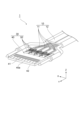
- FIG. 1 is a perspective view showing an optical connector cable according to one embodiment.
- FIG. 2 is a perspective view showing the optical connector cable with the protective member removed.
- FIG. 3 is a plan view of the optical module viewed from above the first surface of the substrate.
- FIG. 4 is a plan view of the optical module viewed from above the second surface of the substrate.
- FIG. 5 is a cross-sectional view of the optical module taken along line VV shown in FIG.
- FIG. 6 is an enlarged view of a portion surrounded by dashed line A shown in FIG. 7 is a perspective view showing a substrate used in the optical module shown in FIG. 3.
- FIG. FIG. 8 is an enlarged view of a portion surrounded by dashed line B shown in FIG.
- FIG. 9 is an enlarged view of a portion surrounded by dashed line C shown in FIG.
- FIG. 10 is a schematic diagram of a partial cross section showing the configuration of an optical module according to the first modified example.
- FIG. 11 is a schematic diagram of a partial cross section showing the configuration of an optical module according to a second modification.
- FIG. 12 is a schematic diagram of a partial cross section showing the configuration of an optical module according to a third modified example.
- FIG. 13A is a plan view showing an example of the inner surface of the lens module used in the third modified example.
- FIG. 13B is a plan view showing another example of the inner surface of the lens module used in the third modified example;
- FIG. 13C is a plan view showing still another example of the inner surface of the lens module used in the third modified example.
- a conventional optical module optically connects an optical fiber and an optical element via a lens provided on the inner surface of the optical module.
- an adhesive is introduced between the substrate and the lens module to fix them together.
- the gap between the substrate and the lens module becomes minute, and it becomes difficult to control the spread of the adhesive introduced into the gap. For this reason, part of the adhesive may flow into the vicinity of the lens provided inside the inner surface of the lens module, blocking the optical path of the lens for optically coupling the optical fiber and the optical element.
- An object of the present disclosure is to provide an optical module and an optical connector cable capable of stably optically coupling an optical fiber and an optical element by preventing obstruction of the lens optical path.
- optical coupling between an optical fiber and an optical element can be stably performed.
- An optical module includes a substrate, an optical element, and a lens module.
- the optical element is mounted on the substrate.
- the lens module has an outer surface and an inner surface facing each other, and a lens provided on the inner surface so as to be optically coupled to the optical element, and optically couples the optical fiber and the optical element via the lens.
- the lens module is mounted on the substrate so that the inner surface faces the substrate, and is attached to the substrate by an adhesive introduced into the gap between the inner surface and the substrate.
- An inflow prevention structure is provided between the substrate and the lens module and between the lens and the adhesive to prevent the adhesive from flowing into the optical axis of the lens.
- an inflow prevention structure is provided between the substrate and the lens module and between the lens and the adhesive to prevent the adhesive from flowing into the optical axis of the lens.
- This inflow prevention structure prevents the adhesive introduced into the gap between the lens module and the substrate from flowing into the lens provided on the inner surface of the lens module, and the lens for optically coupling the optical fiber and the optical element.
- the adhesive does not block the optical path of Therefore, according to this optical module, optical coupling between the optical fiber and the optical element can be stably performed.
- the inflow prevention structure may include a groove or recess provided near the area facing the lens on the surface of the substrate facing the lens module. According to this aspect, it is possible to prevent the adhesive introduced into the gap between the substrate and the lens module from flowing into the optical axis of the lens with a simple configuration. Therefore, according to this optical module, optical coupling between the optical fiber and the optical element can be stably performed with a simple configuration.
- the vicinity of the area referred to here is intended to include not only the area facing the lens but also the area between this facing area and the adhesive.
- the groove or recess which is the inflow prevention structure, may extend along the width direction crossing the longitudinal direction in the plane direction of the substrate, or may extend to the outside in the width direction.
- the inflow prevention structure may include a wall provided between the lens and the adhesive on the inner surface of the lens module. According to this aspect, it is possible to prevent the adhesive introduced into the gap between the substrate and the lens module from flowing into the optical axis of the lens with a simple configuration. Therefore, according to this optical module, optical coupling between the optical fiber and the optical element can be stably performed with a simple configuration.
- the wall which is the inflow prevention structure, may extend along the width direction crossing the longitudinal direction in the surface direction of the lens module, or may extend to the outside in the width direction. The wall may also abut the substrate when the lens module is attached to the substrate with an adhesive. Thereby, the inflow of the adhesive can be prevented more reliably.
- the width of the gap between the substrate and the inner surface of the lens module is 1 mm or less, and the adhesive may be introduced into this gap.
- the substrate and the lens module are mounted thinner, and the optical module can be made thinner. If the adhesive is introduced into such a minute gap, there is a risk that the adhesive will easily reach the interior. The adhesive is prevented from adhering to the optical axis of the optical fiber, and optical coupling between the optical fiber and the optical element can be stably performed.
- the inflow prevention structure may be provided in a region within 5 mm from the optical axis of the lens in the plane direction orthogonal to the optical axis. According to this aspect, it is possible to more reliably attach the lens module to the substrate while ensuring a sufficient amount of adhesive to be introduced between the substrate and the lens module.
- the anti-inflow structure may include a first anti-inflow structure and a second anti-inflow structure, the first anti-inflow structure is arranged on one side with respect to the lens, and the second anti-inflow structure is on the lens. may be arranged on the other side.
- the substrate may be formed with a cavity recessed from the first side of the substrate toward the second side of the substrate to have a bottom, the cavity accommodating at least a portion of the lens module.
- the cavity may have a first cavity and a second cavity having a second bottom located closer to the second surface than the first bottom of the first cavity.
- a lens may be housed in the second cavity.
- the thickness of the optical module can be reduced more reliably.
- the inflow prevention structure may be accommodated in the second cavity.
- the lens module is configured such that light emitted from an optical fiber mounted on the outer surface enters the optical element, or light emitted from the optical element enters the optical fiber mounted on the outer surface. It may have a mirror to change the direction of propagation of the light so that it is incident on the .
- the optical fiber positioned along the substrate and the optical element positioned across the substrate from the optical fiber can be optically coupled using the mirror.
- An optical connector cable includes any one of the optical modules described above and an optical fiber cable.
- a fiber optic cable has at least one optical fiber.
- the optical fiber cable is attached to the optical module so that the optical fiber is optically coupled to the optical element through the lens.
- an inflow prevention structure is provided between the substrate and the lens module and between the lens and the adhesive to prevent the adhesive from flowing into the optical axis of the lens. According to this aspect, it is possible to prevent the adhesive introduced into the gap between the substrate and the lens module from flowing into the lens provided on the inner surface of the lens module. Therefore, according to this optical connector cable, optical coupling between the optical fiber and the optical element can be stably performed.
- FIG. 1 is a perspective view showing an optical connector cable 1 according to one embodiment.
- FIG. 2 is a perspective view showing the optical connector cable 1 with the protective member 20 removed.
- the width direction of the end of the optical connector cable 1 is defined as the direction X
- the extending direction of the end is defined as the direction Y
- the thickness direction of the end is defined as the direction Z.
- direction X, direction Y and direction Z are orthogonal to each other.
- the optical connector cable 1 is a cable used for transmitting and receiving optical signals between devices, for example. As shown in FIGS. 1 and 2, the optical connector cable 1 includes an optical fiber cable 10, a protective member 20, and an optical module 30. FIG. 1 and 2 show one end of the optical fiber cable 10, the other end of the optical fiber cable 10 may have a similar configuration.
- the optical fiber cable 10 has a plurality of optical fibers 11 and a cable jacket 12.
- Each optical fiber 11 is a member for transmitting an optical signal. Most of each optical fiber 11 is housed inside the cable jacket 12 , and the tip portion thereof is exposed to the outside of the cable jacket 12 .
- the plurality of optical fibers 11 are arranged one-dimensionally along the direction X. As shown in FIG. Inside the cable jacket 12, all the optical fibers 11 are housed in close proximity to each other. On the other hand, outside the cable jacket 12 , the plurality of optical fibers 11 are branched into bundles of several (four to six in this embodiment), and the ends of the bundles are held by respective lens modules 50 .
- Each optical fiber 11 may be formed, for example, by coating a glass fiber composed of a core and a clad surrounding the core with a resin.
- Each optical fiber 11 may be a single mode optical fiber (SMF) or a multimode optical fiber (MMF).
- the protection member 20 is a flat member that expands along the direction X and the direction Y, and can accommodate the optical module 30 inside.
- the protective member 20 protects the optical module 30 from external shocks and the like.
- the protective member 20 has a laminated structure consisting of an inner layer 21 and an outer layer 22 covering the inner layer 21 .
- the material of the inner layer 21 may be metal, for example.
- the material of the outer layer 22 may be resin, for example.
- a portion of the inner layer 21 is exposed from the outer layer 22 at the tip of the optical connector cable 1 . This exposed portion is inserted, for example, into a receptacle provided in a device to which the optical connector cable 1 is connected.
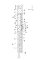
- FIG. 3 is a plan view of the optical module 30 viewed from above the first surface 41 of the substrate 40.
- FIG. 4 is a plan view of the optical module 30 viewed from above the second surface 42 of the substrate 40.
- FIG. FIG. 5 is a cross-sectional view of the optical module 30 taken along line VV shown in FIG.
- FIG. 6 is an enlarged view of a portion surrounded by dashed line A shown in FIG.
- the optical module 30 includes a substrate 40 , multiple lens modules 50 , multiple optical elements 60 , and multiple ICs 61 .
- the substrate 40 is a plate-like member on which various optical elements and electronic elements are mounted.
- the substrate 40 has a first end face 40a and a second end face 40b facing each other in the direction Y, and may be a thin substrate having a thickness of 0.2 mm or more and 0.8 mm or less, for example.
- Various wirings (not shown) for electrically connecting ICs, electronic elements, and the like are provided inside the substrate 40 .
- the end portion where the first end face 40a is located may be referred to as the tip of the optical module 30, and the end portion where the second end face 40b is located may be referred to as the base end of the optical module 30.
- the substrate 40 also has a first surface 41 and a second surface 42 facing each other in the Z direction.
- the surface on which the first surface 41 is positioned is the upper surface of the optical module 30
- the surface on which the second surface 42 is positioned is the lower surface of the optical module 30 .
- the first surface 41 of the substrate 40 is a surface extending along the direction X and the direction Y, and has a rectangular shape in plan view.
- a plurality of patterns 41a which are metal films, are provided in a region of the first surface 41 near the first end surface 40a.
- a plurality of lens modules 50 are placed side by side along the direction X in a region of the first surface 41 near the second end surface 40b.
- the second surface 42 of the substrate 40 is a surface extending along the direction X and the direction Y, and is formed in a rectangular shape in plan view.
- a plurality of optical elements 60 and a plurality of ICs 61 are mounted on a region of the second surface 42 near the second end surface 40b.
- each optical element 60 is indicated by a dashed line for convenience of explanation.
- Each optical element 60 is a light receiving element such as a PD (Photodiode).
- Each optical element 60 overlaps each through hole 48 a provided in the substrate 40 in the thickness direction (direction Z) of the substrate 40 so that the light receiving surface faces the lens module 50 .
- the optical element 60 can receive the light from the lens module 50 facing with the substrate 40 interposed therebetween through the through hole 48a.
- the optical element 60 may be a light emitting element such as a VCSEL (Vertical Cavity Surface Emitting LASER). Since the optical element 60 is arranged on the second surface 42 , the opening area of the through hole 48 a on the second surface 42 is formed to be smaller than the surface area of the optical element 60 .
- Each IC 61 is an integrated circuit that controls the operation of the optical element 60 .
- Each IC 61 may be connected to the optical element 60 via wiring or bonding wires in the substrate 40, for example. In this embodiment, one IC 61 is connected to three optical elements 60 . By arranging the IC 61 near the optical element 60 (for example, arranging it adjacently), a high communication speed between the IC 61 and the optical element 60 can be maintained.
- the lens module 50 is a component that optically couples the optical fiber 11 and the optical element 60 .
- the lens module 50 is made of a material (for example, glass or light-transmitting resin) that transmits light emitted from the optical fiber 11 .
- the lens module 50 reflects the light L emitted from the optical fiber 11 along the direction Y by the mirror 55 provided therein, and converts the propagation direction of the light L to the direction along the direction Z. do.
- the mirror 55 reflects the incident light L in a direction that is 90 degrees with respect to the incident direction.
- the light L reflected by the mirror 55 enters the optical element 60 through the through hole 48 a provided in the substrate 40 .
- the lens module 50 has a groove 51 (outer surface), an upper surface 52 (outer surface), a lower surface 53 (inner surface), an abutment surface 54 , a mirror 55 and a lens 56 .
- the groove portion 51 is a V groove (V-shaped groove on the XZ plane) extending along the direction Y, and is a holding portion that holds the end portion of the optical fiber 11 .
- the groove portion 51 defines the position of the optical fiber 11 with respect to the lens module 50 and prevents misalignment of the optical fiber 11 in the X direction.
- the end of the optical fiber 11 placed in the groove 51 is fixed to the groove 51 with an adhesive, for example.
- the adhesive may be, for example, an ultraviolet curable adhesive or a light transmissive adhesive that transmits the light L emitted from the optical fiber 11 .
- the shape of the groove portion 51 is not limited to the V groove, and may be, for example, a U groove with a rounded bottom, or a rectangular groove having a bottom surface extending along the X direction and the Y direction.
- the holding portion (groove portion 51 in this embodiment) that holds the end portion of the optical fiber 11 does not necessarily have to be provided in the lens module 50 .
- the groove portion 51 may be provided in another component different from the lens module 50 .
- the lens module 50 has a pair of convex portions, and another component provided with the groove portion 51 has a pair of concave portions. may be connected.
- the upper surface 52 is a surface located above the lens module 50 and extends along the X direction and the Y direction.
- the upper surface 52 is positioned closer to the tip of the lens module 50 (right side in FIG. 5) than the groove 51 is.
- the top surface 52 is also provided with a recess having a mirror 55 .
- the lower surface 53 is a surface positioned below the lens module 50 and extends along the X direction and the Y direction. Most of the lower surface 53 faces the groove 51 and the upper surface 52 in the Z direction.
- the abutting surface 54 is a surface against which the tip surface of the optical fiber 11 abuts, and extends along the X direction and the Z direction.
- the abutting surface 54 is provided so as to connect the end of the groove 51 and the end of the upper surface 52 .
- Light L emitted from the optical fiber 11 passes through the abutment surface 54 and enters the mirror 55 .
- the abutment surface 54 and the tip surface of the optical fiber 11 do not have to be in direct contact, and may be fixed to each other via a light-transmitting adhesive or a refractive index matching agent.
- the mirror 55 is a member that changes the propagation direction of the light L emitted from the optical fiber 11 .
- the mirror 55 is provided so as to be inclined with respect to each of the XY plane and the XZ plane.
- the mirror 55 receives the light L emitted along the direction Y from the optical fiber 11 and reflects the light L toward the lens 56 .
- the incident optical axis of the light L and the reflected optical axis may form a right angle, for example.
- the lens 56 is a member optically coupled with the optical element 60 .
- the lens 56 is provided on a portion of the lens module 50 that protrudes downward.
- lens 56 faces optical element 60 in direction Z and has a surface curved convexly toward optical element 60 .
- a focal point F of the lens 56 is located inside the surface of the optical element 60 .
- the lens 56 converges the light L reflected by the mirror 55 and makes it enter the optical element 60 .
- Various parameters of the lens 56 (for example, the surface shape, size, material, etc. of the lens 56) are optimized so that the focal point F of the lens 56 is located inside the optical element 60.
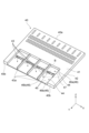
- FIG. 7 is a perspective view showing the substrate 40.
- FIG. FIG. 8 is an enlarged view of a portion surrounded by dashed line B shown in FIG.
- the substrate 40 is provided with a plurality of cavities 43 .
- Each cavity 43 is a depression that is recessed from the first surface 41 toward the second surface 42, and accommodates the lens module 50 therein.
- a plurality of cavities 43 are provided side by side along the direction X.
- the number of cavities 43 may be equal to or greater than the number of lens modules 50 mounted on substrate 40 . In this embodiment, the same number (four) of cavities 43 as the number of lens modules 50 are provided.
- Each cavity 43 may be formed, for example, by counterboring.
- a beam portion 43 a extending from the inside to the outside of the substrate 40 along the direction Y is provided between adjacent cavities 43 .
- the beam portion 43 a has a shape rising from the first bottom portion 45 of each cavity 43 toward the first surface 41 of the substrate 40 .
- Each cavity 43 includes a first cavity 44 and a second cavity 47.
- the first cavity 44 is a depression that forms most of the cavity 43 and has a first bottom 45 and wall surfaces 46 .
- the first bottom portion 45 is a portion on which the lens module 50 is placed, and is a flat surface extending along the X direction and the Y direction in this embodiment.
- the first bottom portion 45 has a rectangular outer edge with long sides extending in the direction Y, and has a size that allows the entire lens module 50 to be placed thereon. Note that the lens module 50 is placed on the first bottom portion 45 not only when the lens module 50 is placed on the first bottom portion 45 so as to be in direct contact with the first bottom portion 45, but also when the lens module 50 is placed on the first bottom portion 45 via a member such as an adhesive. This includes the case where the lens module 50 is placed on the bottom portion 45 .
- the first bottom portion 45 has a pair of positioning holes 45a.
- Each positioning hole 45a is a hole penetrating from the first bottom 45 toward the second surface 42 (see FIG. 4).
- the pair of positioning holes 45 a functions as a positioning mechanism for the lens module 50 with respect to the cavity 43 .
- the lens module 50 is provided with a pair of convex portions corresponding to the pair of positioning holes 45a.
- the provided lens 56 (see FIG. 5) and the optical element 60 may be preferably optically coupled.
- the number of positioning holes 45a may be one, the lens module 50 can be positioned more accurately by forming two or more positioning holes 45a.
- Each positioning hole 45a does not need to penetrate from the first bottom portion 45 to the second surface 42, and may be a non-through hole having a bottom surface.
- the aspect of the positioning mechanism used for positioning the lens module 50 is not limited to the positioning holes 45a.
- the lens 56 of the lens module 50 and the optical element 60 are preferably optically coupled. It may be a mode to do.
- the material of the lens module 50 is a material that transmits visible light (for example, glass or light-transmitting resin). There may be.
- the wall surface 46 is a surface rising from the outer edge of the first bottom portion 45 toward the first surface 41 of the substrate 40 .
- the wall surface 46 has a first wall surface 46a and a pair of second wall surfaces 46b.
- the first wall surface 46a is a wall surface provided at the end of the first cavity 44 near the first end surface 40a, and extends along the X direction and the Z direction.
- the first wall surface 46 a faces the tip surface of the lens module 50 accommodated in the cavity 43 .
- the first wall surface 46a does not have to contact the lens module 50 accommodated in the cavity 43, and a gap may be provided between the first wall surface 46a and the lens module 50.
- FIG. A corner portion where the first wall surface 46a and the first bottom portion 45 intersect may have an R shape.
- the pair of second wall surfaces 46b are wall surfaces facing each other in the X direction and extend along the Y and Z directions.
- the second wall surface 46 b faces the side surface of the lens module 50 accommodated in the cavity 43 .
- the second wall surface 46b does not have to contact the lens module 50 accommodated in the cavity 43, and a gap may be provided between the second wall surface 46b and the lens module 50.
- FIG. A corner portion where the second wall surface 46b and the first bottom portion 45 intersect may have an R shape.
- No wall surface is provided at the end of the first cavity 44 near the second end face 40b. That is, the cavity 43 is open at the second end surface 40b.
- the lens module 50 can be accommodated from the opening toward the inside of the cavity 43 .
- the optical fiber 11 connected to the lens module 50 can be drawn out of the cavity 43 through the opening.
- the second cavity 47 is a depression provided in the first bottom portion 45 of the first cavity 44 .
- the second cavity 47 is formed to extend along the X direction.
- the second cavity 47 has a second bottom 48 closer to the second surface 42 than the first bottom 45 of the first cavity 44 .
- the second bottom portion 48 is a flat surface extending along the X direction and the Y direction.
- a portion of the lens module 50 (the portion protruding downward along the direction Z) is placed on the second bottom portion 48 (see FIG. 5).
- the second bottom portion 48 is provided with a plurality of through holes 48a. Two round holes and one elongated hole are provided as through holes 48 a for each second cavity 47 .
- the number and shape of the through-holes 48a are not limited to this, and may be changed as appropriate according to the number or shape of the optical elements 60 (see FIG. 4) mounted on the second surface .
- the through hole 48a penetrates from the second bottom portion 48 toward the second surface 42.
- Light L directed from the lens 56 to the optical element 60 passes through the through hole 48a.
- the through hole 48 a has a tapered shape with an inner diameter that decreases from the second bottom portion 48 toward the second surface 42 .
- the inner diameter and taper angle of the through hole 48 a are optimized to a size that does not block the path of the light L from the lens 56 to the optical element 60 .
- the through hole 48a may be a straight through hole having a constant inner diameter.
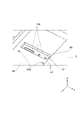
- FIG. 9 is an enlarged view of a portion surrounded by dashed line C shown in FIG.
- the lens module 50 is mostly accommodated in the first cavity 44, and has a protruding portion 57 (a portion protruding downward along the direction Z) provided with a lens 56. is accommodated in the second cavity 47 .
- the entire structure of the lens module 50 is located on the substrate 40, but the base end portion (the left end portion in FIG. 5) of the lens module 50 may protrude outside the substrate 40. .
- Adhesives S 1 and S 2 are provided between the lower surface 53 of the lens module 50 and the first bottom 45 of the first cavity 44 to fix the lens module 50 to the cavity 43 of the substrate 40 .
- the adhesives S1, S2 may be UV curable adhesives, for example.
- the protruding portion 57 is formed between the substrate 40 and the lens module 50 and between the lens 56 and the adhesives S1 and S2 in the region between the first wall 57a (flow prevention structure, first flow prevention structure) and the second wall 57a.
- wall 57b inflow prevention structure, second inflow prevention structure.
- Each of the tip of the first wall 57a and the tip of the second wall 57b abuts on the second bottom 48 of the second cavity 47 (inflow prevention structure), which is a recess, and moves along the direction X in the second cavity 47. It extends in the width direction.
- the first wall 57a and the second wall 57b may extend to the side surface of the second cavity 47 along the X direction.
- the adhesives S1 and S2 introduced between the substrate 40 and the lens module 50 do not flow into the optical axis L1 of the lens 56, and the space S is ensured.
- the first wall 57a and the second wall 57b are provided close to the lens 56.
- the distance from the optical axis L1 of the lens to the outer walls of the first wall 57a and the second wall 57b along the direction Y is 5 mm. may be within
- the width along the Z direction of the gap between the substrate 40 into which the adhesives S1 and S2 are introduced and the lens module 50 may be 1 mm or less.
- a portion (mounting portion) of the optical fiber 11 located on the substrate 40 extends along the first surface 41 of the substrate 40 and its central axis is located inside the cavity 43 . Thereby, the end portion of the optical fiber 11 extends straight without bending at the second end surface 40 b of the substrate 40 .
- the depth D1 of the first cavity 44 is optimized according to the thickness of the lens module 50, for example.
- the depth D1 of the first cavity 44 is the distance from the first surface 41 to the first bottom 45 in the thickness direction (direction Z) of the substrate 40 .
- the depth D1 of the first cavity 44 is at least half the thickness of the substrate 40 (the distance from the first surface 41 to the second surface 42).
- the depth D1 of the first cavity 44 may be 6 or more and 8 or less.
- the depth D1 of the first cavity 44 may be half or more the thickness T of the lens module 50 .
- the thickness T of the lens module 50 is the distance from the upper surface 52 to the lower surface 53 in the Z direction.
- the optical module 30 is made thinner.
- the upper surface 52 of the lens module 50 is positioned outside the cavity 43 (above the first surface 41 of the substrate 40), but the upper surface 52 is positioned inside the cavity 43 (above the first surface 41 of the substrate 40). 41 or below the first surface 41), the depth D1 of the first cavity 44 may be further increased.
- the depth D2 of the second cavity 47 is greater than the depth D1 of the first cavity 44.
- the depth D2 of the second cavity 47 is the distance from the first surface 41 to the second bottom 48 in the thickness direction of the substrate 40 .
- the depth D2 of the second cavity 47 may be optimized according to the thickness of the lens module 50, for example. For example, when the thickness T of the substrate 40 is 10, the depth D2 of the second cavity 47 may be, for example, 7 or more and 9 or less.
- the optical axis L1 of the lens 56 is formed between the substrate 40 and the lens module 50, and between the lens 56 and the adhesives S1 and S2, the optical axis L1 of the lens 56 is formed.
- a first wall 57a and a second wall 57b are provided as an inflow prevention structure for preventing the inflow of the adhesives S1 and S2.
- This inflow prevention structure prevents the adhesives S1 and S2 introduced into the gap between the lens module 50 and the substrate 40 from flowing into the lens 56 provided on the inner surface of the lens module 50.
- the adhesives S1 and S2 do not block the optical path of the lens 56 for optically coupling the lens 60 with the adhesives S1 and S2.
- the second cavity 47 also functions as an inflow prevention structure, and when the amount of the adhesives S1 and S2 is small, the inflow of the adhesives can be prevented by itself.
- the width of the gap between the substrate 40 and the lower surface 53 of the lens module 50 may be 1 mm or less, and the adhesives S1 and S2 are introduced into this gap.
- the substrate 40 and the lens module 50 are mounted thinner, and the thickness of the optical module 30 and the like can be reduced. If the adhesive is introduced into such a minute gap, the adhesive may easily reach the inside.
- the optical module 30 according to the present embodiment is provided with the inflow prevention structure described above. Therefore, the adhesive is prevented from adhering to the optical axis L1 of the lens 56, and optical coupling between the optical fiber 11 and the optical element 60 can be stably performed.
- the first wall 57a and the second wall 57b which are inflow prevention structures, are located within 5 mm from the optical axis L1 of the lens 56 in the Y direction orthogonal to the optical axis L1. may be provided in the area of In this case, a sufficient amount of the adhesives S1 and S2 introduced between the substrate 40 and the lens module 50 can be ensured, and the lens module 50 can be attached to the substrate 40 more reliably.
- the cavity 43 recessed in the thickness direction (direction Z) of the substrate 40 is provided, and at least part of the lens module 50 is accommodated inside the cavity 43. .
- the thickness of the optical module 30 is reduced by the amount of the lens module 50 accommodated in the cavity 43, and the thickness is reduced. Accordingly, the thickness of the optical connector cable 1 including the optical module 30 is also reduced.
- the lens module is placed on the flat surface of the substrate.
- the optical module 30 since there is a large gap between the height of the optical fiber extending outside the substrate and the height of the end of the optical fiber mounted on the substrate, it is not necessary to bend the optical fiber significantly (need to increase the curvature). be.
- the lens module 50 since the lens module 50 is housed in the cavity 43 of the substrate 40, the height of the optical fiber 11 mounted on the substrate 40 is reduced, and the gap is reduced. .
- the mounting position of the optical fiber on the substrate is high as described above. Therefore, when it is attempted to gently bend the optical fiber to reduce the bending, the arrangement space along the axial direction of the optical fiber becomes large.
- the optical module 30 since the mounting position of the optical fiber 11 on the substrate 40 is lower than in the conventional example, the space for arranging the optical fiber 11 along the axial direction can be reduced. Thereby, miniaturization of the optical module 30 can be achieved.
- the present invention is not limited to the above embodiments and can be applied to various embodiments.
- the lens module 50 is placed in the cavity 43 provided in the substrate 40, but the present invention is not limited to this. That is, as shown in the following first modification, second modification 2, and third modification 3, the present invention may be applied to a configuration in which the lens module 50 is placed as it is on the surface of the substrate.
- FIG. 10 is a diagram showing an optical module according to a first modified example.
- a lens module 150A is placed on the surface of a substrate 140A.
- a recess 141 is provided in the substrate 140A, and a first wall 142a and a second wall 142b (inflow prevention structure) are provided in the recess 141.
- the inflow prevention structure prevents the adhesives S1 and S2 from flowing into the optical axis L1 of the lens 56 between the substrate 140A and the lens module 150A and between the lens 56 and the adhesives S1 and S2.
- a first wall 142a and a second wall 142b are provided.
- the first wall 142a and the second wall 142b extend in the X direction.
- the lens module 150A does not have walls on its inner surface.
- the optical element 60 can be provided at the bottom of the concave portion 141 and at a location facing the lens 56 .
- the inflow prevention structure prevents the adhesives S1 and S2 introduced into the gap between the lens module 150A and the substrate 140A from flowing into the lens 56 provided on the inner surface of the lens module 150A. be. Further, the adhesives S1 and S2 do not obstruct the optical path of the lens 56 for optically coupling the optical fiber 11 and the optical element 60 together. Therefore, according to the optical module 130A according to the first modified example and the optical connector cable 1 including the optical module 130A, optical coupling between the optical fiber 11 and the optical element 60 can be stably performed.
- a groove extending in the X direction is formed by the recess 141, the first wall 142a, and the second wall 142b, and functions as an inflow prevention structure.
- FIG. 11 is a diagram showing a glowing module according to a second modified example.
- a lens module 150B is placed on the surface of a substrate 140B.
- a recess or the like is not provided in the substrate 140B.
- the lens module 150B is provided with a first wall 151a and a second wall 151b (inflow prevention structure) on the inner surface. That is, the inflow prevention structure prevents the adhesives S1 and S2 from flowing into the optical axis L1 of the lens 56 between the substrate 140B and the lens module 150B and between the lens 56 and the adhesives S1 and S2.
- a first wall 151a and a second wall 151b are provided.
- the first wall 151a and the second wall 151b extend in the X direction.
- the optical element 60 may be provided on the second surface of the substrate 140B like the optical module 30, but may be provided on the first surface (inner surface) facing the lens module 150B.
- the inflow prevention structure prevents the adhesives S1 and S2 introduced into the gap between the lens module 150B and the substrate 140B from flowing into the lens 56 provided on the inner surface of the lens module 150B. be. Further, the adhesives S1 and S2 do not obstruct the optical path of the lens 56 for optically coupling the optical fiber 11 and the optical element 60 together. Therefore, according to the optical module 130B according to the second modified example and the optical connector cable 1 including the optical module 130B, optical coupling between the optical fiber 11 and the optical element 60 can be stably performed.
- FIG. 12 is a diagram showing an optical module according to a third modified example.
- FIG. 13A is a plan view showing an example of the inner surface of the lens module used in the third modified example.
- FIG. 13B is a plan view showing another example of the inner surface of the lens module used in the third modified example;
- FIG. 13C is a plan view showing still another example of the inner surface of the lens module used in the third modified example.
- a lens module 150C is mounted on the surface of a substrate 140B.
- the substrate 140B is not provided with recesses or the like as in the second modification.
- the lens module 150C is provided with a first guide groove 152a and a second guide groove 152b (inflow prevention structure) on the inner surface. That is, the inflow prevention structure prevents the adhesives S1 and S2 from flowing into the optical axis L1 of the lens 56 between the substrate 140B and the lens module 150C and between the lens 56 and the adhesives S1 and S2.
- a first guide groove 152a and a second guide groove 152b are provided.
- the first guide groove 152a and the second guide groove 152b extend in the X direction.
- the optical element 60 may be provided on the second surface of the substrate 140B like the optical module 30, but may be provided on the first surface (inner surface) facing the lens module 150C.
- the inflow prevention structure prevents the adhesives S1 and S2 introduced into the gap between the lens module 150C and the substrate 140B from flowing into the lens 56 provided on the inner surface of the lens module 150C. be. Further, the adhesives S1 and S2 do not obstruct the optical path of the lens 56 for optically coupling the optical fiber 11 and the optical element 60 together. Therefore, according to the optical module 130C according to the third modification and the optical connector cable 1 including the optical module 130C, optical coupling between the optical fiber 11 and the optical element 60 can be stably performed.
- the guide grooves provided in the lens module are not limited to the structure shown in FIG. 13A, and may have the structures shown in FIGS. 13B and 13C. That is, as shown in FIG. 13B, the guide groove 153 of the lens module 150D may have a shape that forms two sides of a triangle. Also, as shown in FIG. 13C, the guide groove 154 of the lens module 150E may be convex.
- the optical module of any one of the above embodiments and the first to third modifications has a configuration in which the light L emitted from the optical fiber 11 is incident on the optical element 60.
- a configuration in which light is incident on the optical fiber 11 may be employed.
- the optical element 60 may be a light emitting element such as a VCSEL (Vertical Cavity Surface Emitting LASER).
- the light emitted from the optical element 60 may be converted into collimated light (parallel light) by the lens 56 and may enter the optical fiber 11 after being reflected by the mirror 55 .
- Reference Signs List 1 Optical connector cable 10
- Optical fiber cable 11 Optical fiber 12 Cable jacket 20
- Protective member 21 Inner layer 22
Abstract
An optical module (30) comprises a substrate (40), an optical element (60), and a lens module (50). The optical element (60) is mounted on the substrate (40). The lens module (50) has an outer surface (52) and an inner surface (53) facing each other, and a lens (56) provided to the inner surface so as to be optically coupled to the optical element (60), and an optical fiber (11) and the optical element (60) are optically coupled via a lens (56). The lens module (50) is mounted on the substrate (40) so that the inner surface (53) faces the substrate (40), and the lens module (50) is attached to the substrate (40) by adhesives (S1, S2) which are introduced into a gap between the inner surface (53) and the substrate (40). Inflow prevention structures (47, 57) for preventing inflow of the adhesives (S1, S2) toward the optical axis of the lens (56) are provided between the substrate (40) and the lens module (50) and between the lens (56) and the adhesives (S1, S2).
Description
本開示は、光モジュール及び光コネクタケーブルに関する。本出願は、2021年8月5日出願の日本出願第2021-128962号に基づく優先権を主張し、前記日本出願に記載された全ての記載内容を援用する。
The present disclosure relates to optical modules and optical connector cables. This application claims priority based on Japanese Application No. 2021-128962 filed on August 5, 2021, and incorporates all the descriptions described in the Japanese Application.
特許文献1には、基板に搭載された光電変換素子(光素子)に対して光ファイバを光学的に接続する光学部品(光モジュール)の一例が開示されている。この光学部品は、光ファイバから水平方向に出射された光をレンズ部品によって垂直方向に伝搬する光へと変換し、この光を基板に搭載された光電変換素子へと入射させる。
Patent Document 1 discloses an example of an optical component (optical module) that optically connects an optical fiber to a photoelectric conversion element (optical element) mounted on a substrate. This optical component converts the light emitted horizontally from the optical fiber into light propagating in the vertical direction by means of the lens component, and makes this light incident on the photoelectric conversion element mounted on the substrate.
本開示の光モジュールは、基板、光素子、及び、レンズモジュールを備える。光素子は、基板に搭載される。レンズモジュールは、互いに対向する外表面及び内面と、光素子に光学的に結合するように内面に設けられるレンズとを有し、レンズを介して光ファイバと光素子とを光学的に結合する。レンズモジュールは、内面が基板に対向するように基板に搭載されると共に、内面と基板との隙間に導入された接着剤により基板に取り付けられる。基板とレンズモジュールとの間であって且つレンズと接着剤との間に、レンズの光軸への接着剤の流入を防止する流入防止構造が設けられている。
The optical module of the present disclosure includes a substrate, an optical element, and a lens module. The optical element is mounted on the substrate. The lens module has an outer surface and an inner surface facing each other, and a lens provided on the inner surface so as to be optically coupled to the optical element, and optically couples the optical fiber and the optical element via the lens. The lens module is mounted on the substrate so that the inner surface faces the substrate, and is attached to the substrate by an adhesive introduced into the gap between the inner surface and the substrate. An inflow prevention structure is provided between the substrate and the lens module and between the lens and the adhesive to prevent the adhesive from flowing into the optical axis of the lens.
本開示の光コネクタケーブルは、上述の光モジュールと、光ファイバケーブルと、を備える。光ファイバケーブルは、少なくとも1つの光ファイバを有する。この光コネクタケーブルでは、光ファイバがレンズを介して光素子と光学的に結合するように光ファイバケーブルが光モジュールに取り付けられる。
An optical connector cable of the present disclosure includes the optical module described above and an optical fiber cable. A fiber optic cable has at least one optical fiber. In this optical connector cable, the optical fiber cable is attached to the optical module so that the optical fiber is optically coupled to the optical element through the lens.
[本開示が解決しようとする課題]
従来の光モジュールは、光ファイバと光素子とを光モジュールの内面に設けたレンズを介して光学的に接続している。このような光モジュールでは、基板に対してレンズモジュールを実装する際、基板とレンズモジュールとの間に接着剤を導入して両者を固定する。しかしながら、光モジュールの薄形化に伴い、基板とレンズモジュールとの隙間が微小になり、隙間に導入された接着剤の広がりを制御することが難しくなってきている。このため、接着剤の一部がレンズモジュール内面の内側に設けたレンズ付近まで流入し、光ファイバと光素子とを光結合するためのレンズの光路を阻害してしまう場合がある。 [Problems to be Solved by the Present Disclosure]
A conventional optical module optically connects an optical fiber and an optical element via a lens provided on the inner surface of the optical module. In such an optical module, when the lens module is mounted on the substrate, an adhesive is introduced between the substrate and the lens module to fix them together. However, as the optical module becomes thinner, the gap between the substrate and the lens module becomes minute, and it becomes difficult to control the spread of the adhesive introduced into the gap. For this reason, part of the adhesive may flow into the vicinity of the lens provided inside the inner surface of the lens module, blocking the optical path of the lens for optically coupling the optical fiber and the optical element.
本開示は、レンズ光路の阻害を防止して、光ファイバと光素子との光結合を安定的に行うことができる、光モジュール及び光コネクタケーブルを提供することを目的とする。
An object of the present disclosure is to provide an optical module and an optical connector cable capable of stably optically coupling an optical fiber and an optical element by preventing obstruction of the lens optical path.
[本開示の効果]
本開示によれば、光ファイバと光素子との間の光結合を安定的に行うことができる。 [Effect of the present disclosure]
According to the present disclosure, optical coupling between an optical fiber and an optical element can be stably performed.
本開示によれば、光ファイバと光素子との間の光結合を安定的に行うことができる。 [Effect of the present disclosure]
According to the present disclosure, optical coupling between an optical fiber and an optical element can be stably performed.
[本開示の実施形態の説明]
最初に、本開示の実施形態の内容を列記して説明する。一実施形態に係る光モジュールは、基板、光素子、及び、レンズモジュールを備える。光素子は、基板に搭載される。レンズモジュールは、互いに対向する外表面及び内面と、光素子に光学的に結合するように内面に設けられたレンズとを有し、レンズを介して光ファイバと光素子とを光学的に結合する。レンズモジュールは、内面が基板に対向するように基板に搭載されると共に、内面と基板との隙間に導入された接着剤により基板に取り付けられる。基板とレンズモジュールとの間であって且つレンズと接着剤との間に、レンズの光軸への接着剤の流入を防止する流入防止構造が設けられている。 [Description of Embodiments of the Present Disclosure]
First, the contents of the embodiments of the present disclosure will be listed and described. An optical module according to one embodiment includes a substrate, an optical element, and a lens module. The optical element is mounted on the substrate. The lens module has an outer surface and an inner surface facing each other, and a lens provided on the inner surface so as to be optically coupled to the optical element, and optically couples the optical fiber and the optical element via the lens. . The lens module is mounted on the substrate so that the inner surface faces the substrate, and is attached to the substrate by an adhesive introduced into the gap between the inner surface and the substrate. An inflow prevention structure is provided between the substrate and the lens module and between the lens and the adhesive to prevent the adhesive from flowing into the optical axis of the lens.
この光モジュールでは、基板とレンズモジュールとの間であって且つレンズと接着剤との間に、レンズの光軸への接着剤の流入を防止する流入防止構造が設けられている。この流入防止構造により、レンズモジュールと基板との隙間に導入された接着剤がレンズモジュールの内面に設けられたレンズまで流入することが防止され、光ファイバと光素子とを光結合するためのレンズの光路を接着剤が阻害することがない。よって、この光モジュールによれば、光ファイバと光素子との間の光結合を安定的に行うことができる。
In this optical module, an inflow prevention structure is provided between the substrate and the lens module and between the lens and the adhesive to prevent the adhesive from flowing into the optical axis of the lens. This inflow prevention structure prevents the adhesive introduced into the gap between the lens module and the substrate from flowing into the lens provided on the inner surface of the lens module, and the lens for optically coupling the optical fiber and the optical element. The adhesive does not block the optical path of Therefore, according to this optical module, optical coupling between the optical fiber and the optical element can be stably performed.
一実施形態として、流入防止構造は、基板のレンズモジュールに対向する面であってレンズに対向する領域付近に設けられた溝又は凹部を含んでもよい。この態様によれば、基板とレンズモジュールとの隙間に導入された接着剤がレンズの光軸まで流入してしまうことを簡易な構成によって防止することができる。よって、この光モジュールによれば、光ファイバと光素子との間の光結合を簡易な構成で安定的に行うことができる。なお、ここでいう領域付近とは、レンズに対向する領域だけでなく、この対向領域と接着剤との間の領域を含む趣旨である。また、流入防止構造である溝又は凹部は、基板の面方向において長手方向と交差する幅方向に沿って延在していてもよいし、幅方向の外側まで延在していてもよい。
As one embodiment, the inflow prevention structure may include a groove or recess provided near the area facing the lens on the surface of the substrate facing the lens module. According to this aspect, it is possible to prevent the adhesive introduced into the gap between the substrate and the lens module from flowing into the optical axis of the lens with a simple configuration. Therefore, according to this optical module, optical coupling between the optical fiber and the optical element can be stably performed with a simple configuration. The vicinity of the area referred to here is intended to include not only the area facing the lens but also the area between this facing area and the adhesive. Further, the groove or recess, which is the inflow prevention structure, may extend along the width direction crossing the longitudinal direction in the plane direction of the substrate, or may extend to the outside in the width direction.
一実施形態として、流入防止構造は、レンズモジュールの内面であってレンズと接着剤との間に設けられた壁を含んでもよい。この態様によれば、基板とレンズモジュールとの隙間に導入された接着剤がレンズの光軸まで流入してしまうことを簡易な構成によって防止することができる。よって、この光モジュールによれば、光ファイバと光素子との間の光結合を簡易な構成で安定的に行うことができる。流入防止構造である壁は、レンズモジュールの面方向において長手方向と交差する幅方向に沿って延在していてもよいし、幅方向の外側まで延在していてもよい。また、この壁は、レンズモジュールが接着剤により基板に取り付けられた際に基板に当接してもよい。これにより、接着剤の流入をより確実に防止することができる。
In one embodiment, the inflow prevention structure may include a wall provided between the lens and the adhesive on the inner surface of the lens module. According to this aspect, it is possible to prevent the adhesive introduced into the gap between the substrate and the lens module from flowing into the optical axis of the lens with a simple configuration. Therefore, according to this optical module, optical coupling between the optical fiber and the optical element can be stably performed with a simple configuration. The wall, which is the inflow prevention structure, may extend along the width direction crossing the longitudinal direction in the surface direction of the lens module, or may extend to the outside in the width direction. The wall may also abut the substrate when the lens module is attached to the substrate with an adhesive. Thereby, the inflow of the adhesive can be prevented more reliably.
一実施形態として、流入防止構造は、レンズモジュールの内面であってレンズと接着剤との間に設けられた誘導溝を含んでもよい。この態様によれば、基板とレンズモジュールとの隙間に導入された接着剤がレンズの光軸まで流入してしまうことを簡易な構成によって防止することができる。よって、この光モジュールによれば、光ファイバと光素子との間の光結合を簡易な構成で安定的に行うことができる。流入防止構造である誘導溝は、レンズモジュールの面方向において長手方向と交差する幅方向に沿って延在していてもよいし、幅方向の外側まで延在していてもよい。なお、流入防止構造としては、上述した溝又は凹部、壁、及び、誘導溝のいずれか2つ又は3つを組み合わせた構造であってもよい。
As one embodiment, the inflow prevention structure may include a guide groove provided between the lens and the adhesive on the inner surface of the lens module. According to this aspect, it is possible to prevent the adhesive introduced into the gap between the substrate and the lens module from flowing into the optical axis of the lens with a simple configuration. Therefore, according to this optical module, optical coupling between the optical fiber and the optical element can be stably performed with a simple configuration. The guide groove, which is an inflow prevention structure, may extend along the width direction crossing the longitudinal direction in the plane direction of the lens module, or may extend to the outside in the width direction. The inflow prevention structure may be a structure in which any two or three of the above-described grooves or recesses, walls, and guide grooves are combined.
一実施形態として、基板とレンズモジュールの内面との隙間の幅が1mm以下であり、接着剤がこの隙間に導入されていてもよい。この態様によれば、基板とレンズモジュールとがより薄く取り付けられることになり、光モジュールを薄形化することができる。なお、このような微小な隙間に接着剤を導入すると接着剤が内部まで容易に到達してしまう虞があるが、本実施形態に係る光モジュールには流入防止構造が設けられているため、レンズの光軸に接着剤が付着することが防止されており、光ファイバと光素子との光結合を安定的に行うことが可能となる。
As one embodiment, the width of the gap between the substrate and the inner surface of the lens module is 1 mm or less, and the adhesive may be introduced into this gap. According to this aspect, the substrate and the lens module are mounted thinner, and the optical module can be made thinner. If the adhesive is introduced into such a minute gap, there is a risk that the adhesive will easily reach the interior. The adhesive is prevented from adhering to the optical axis of the optical fiber, and optical coupling between the optical fiber and the optical element can be stably performed.
一実施形態として、流入防止構造は、レンズの光軸から、その光軸に直交する面方向に5mm以内の領域に設けられていてもよい。この態様によれば、基板とレンズモジュールとの間に導入される接着剤の量を十分に確保しつつ、基板に対してレンズモジュールをより確実に取り付けることができる。
As one embodiment, the inflow prevention structure may be provided in a region within 5 mm from the optical axis of the lens in the plane direction orthogonal to the optical axis. According to this aspect, it is possible to more reliably attach the lens module to the substrate while ensuring a sufficient amount of adhesive to be introduced between the substrate and the lens module.
一実施形態として、流入防止構造は、第1流入防止構造と第2流入防止構造とを含んでもよく、第1流入防止構造はレンズに対して一方に配置され、第2流入防止構造はレンズに対して他方に配置されてもよい。この態様によれば、基板とレンズモジュールとの間においてレンズの一方及び他方に導入される接着剤の何れもレンズの光軸領域に流入してしまうことを防止することができる。よって、この光モジュールによれば、光ファイバと光素子とをより安定して光結合させることができる。
As an embodiment, the anti-inflow structure may include a first anti-inflow structure and a second anti-inflow structure, the first anti-inflow structure is arranged on one side with respect to the lens, and the second anti-inflow structure is on the lens. may be arranged on the other side. According to this aspect, it is possible to prevent any of the adhesive introduced into one or the other lens between the substrate and the lens module from flowing into the optical axis region of the lens. Therefore, according to this optical module, the optical fiber and the optical element can be optically coupled more stably.
一実施形態として、基板には、底部を有するように基板の第1面から基板の第2面に向かって窪むキャビティが形成されてもよく、キャビティにはレンズモジュールの少なくとも一部が収容されてもよい。キャビティは、第1キャビティと、第1キャビティの第1底部よりも第2面の近くに位置している第2底部を有する第2キャビティとを有してもよい。レンズは、第2キャビティに収容されていてもよい。この場合、光モジュールをより確実に薄型化することができる。また、この実施形態において、流入防止構造は、第2キャビティに収容されていてもよい。
In one embodiment, the substrate may be formed with a cavity recessed from the first side of the substrate toward the second side of the substrate to have a bottom, the cavity accommodating at least a portion of the lens module. may The cavity may have a first cavity and a second cavity having a second bottom located closer to the second surface than the first bottom of the first cavity. A lens may be housed in the second cavity. In this case, the thickness of the optical module can be reduced more reliably. Also, in this embodiment, the inflow prevention structure may be accommodated in the second cavity.
一実施形態として、レンズモジュールは、外表面に搭載される光ファイバから出射された光が光素子へと入射するように、又は、光素子から出射された光が外表面に搭載された光ファイバへと入射するように光の伝搬方向を変換するミラーを有していてもよい。この態様によれば、基板に沿って位置する光ファイバと、光ファイバに対して基板を挟んで位置する光素子とをミラーを用いて光学的に結合することができる。
As one embodiment, the lens module is configured such that light emitted from an optical fiber mounted on the outer surface enters the optical element, or light emitted from the optical element enters the optical fiber mounted on the outer surface. It may have a mirror to change the direction of propagation of the light so that it is incident on the . According to this aspect, the optical fiber positioned along the substrate and the optical element positioned across the substrate from the optical fiber can be optically coupled using the mirror.
一実施形態に係る光コネクタケーブルは、上述したいずれかの光モジュールと、光ファイバケーブルと、を備える。光ファイバケーブルは、少なくとも1つの光ファイバを有する。この光コネクタケーブルでは、光ファイバがレンズを介して光素子と光学的に結合するように光ファイバケーブルが光モジュールに取り付けられる。
An optical connector cable according to one embodiment includes any one of the optical modules described above and an optical fiber cable. A fiber optic cable has at least one optical fiber. In this optical connector cable, the optical fiber cable is attached to the optical module so that the optical fiber is optically coupled to the optical element through the lens.
この光コネクタケーブルでは、基板とレンズモジュールとの間であって且つレンズと接着剤との間に、レンズの光軸への接着剤の流入を防止する流入防止構造が設けられている。この態様によれば、基板とレンズモジュールとの隙間に導入された接着剤がレンズモジュールの内面に設けられたレンズまで流入してしまうことを防止することができる。よって、この光コネクタケーブルによれば、光ファイバと光素子との光結合を安定的に行うことができる。
In this optical connector cable, an inflow prevention structure is provided between the substrate and the lens module and between the lens and the adhesive to prevent the adhesive from flowing into the optical axis of the lens. According to this aspect, it is possible to prevent the adhesive introduced into the gap between the substrate and the lens module from flowing into the lens provided on the inner surface of the lens module. Therefore, according to this optical connector cable, optical coupling between the optical fiber and the optical element can be stably performed.
[本開示の実施形態の詳細]
本開示に係る光モジュール及び光コネクタケーブルの具体例を、以下に図面を参照しつつ説明する。本発明はこれらの例示に限定されるものではなく、請求の範囲によって示され、請求の範囲と均等の意味および範囲内でのすべての変更が含まれることが意図される。図面の説明においては同一要素には同一符号を付し、重複する説明を省略する。 [Details of the embodiment of the present disclosure]
Specific examples of the optical module and optical connector cable according to the present disclosure will be described below with reference to the drawings. The present invention is not limited to these examples, but is indicated by the scope of the claims, and is intended to include all modifications within the meaning and scope of equivalents of the scope of the claims. In the description of the drawings, the same elements are denoted by the same reference numerals, and overlapping descriptions are omitted.
図1及び図2を参照して、一実施形態に係る光コネクタケーブル1について説明する。図1は、一実施形態に係る光コネクタケーブル1を示す斜視図である。図2は、保護部材20を除去した光コネクタケーブル1を示す斜視図である。以下、説明のために、光コネクタケーブル1の端部の幅方向を方向Xとし、当該端部の延在方向を方向Yとし、当該端部の厚み方向を方向Zとする。本実施形態においては、方向X、方向Y及び方向Zは互いに直交している。
An optical connector cable 1 according to one embodiment will be described with reference to FIGS. FIG. 1 is a perspective view showing an optical connector cable 1 according to one embodiment. FIG. 2 is a perspective view showing the optical connector cable 1 with the protective member 20 removed. Hereinafter, for the sake of explanation, the width direction of the end of the optical connector cable 1 is defined as the direction X, the extending direction of the end is defined as the direction Y, and the thickness direction of the end is defined as the direction Z. In this embodiment, direction X, direction Y and direction Z are orthogonal to each other.
光コネクタケーブル1は、例えばデバイス間において光信号を送受信する際に使用するケーブルである。図1及び図2に示すように、光コネクタケーブル1は、光ファイバケーブル10、保護部材20、及び光モジュール30を備えている。図1及び図2では、光ファイバケーブル10の一端を示しているが、光ファイバケーブル10の他端も同様の構成を有していてもよい。
The optical connector cable 1 is a cable used for transmitting and receiving optical signals between devices, for example. As shown in FIGS. 1 and 2, the optical connector cable 1 includes an optical fiber cable 10, a protective member 20, and an optical module 30. FIG. 1 and 2 show one end of the optical fiber cable 10, the other end of the optical fiber cable 10 may have a similar configuration.
図2に示すように、光ファイバケーブル10は、複数の光ファイバ11及びケーブル外被12を有する。各光ファイバ11は、光信号を伝達するための部材である。各光ファイバ11は、その大部分がケーブル外被12の内部に収容され、先端部分がケーブル外被12の外部に露出している。複数の光ファイバ11は、方向Xに沿って一次元状に並んで配置されている。ケーブル外被12の内部では、全ての光ファイバ11が互いに密接してまとまって収容されている。一方、ケーブル外被12の外部においては、複数の光ファイバ11は数本(本実施形態においては4本から6本)の束に分岐し、それぞれの束の端部が各レンズモジュール50によって保持されている。各光ファイバ11は、例えば、コア及び当該コアを囲むクラッドからなるガラスファイバを、樹脂で被覆することにより形成されてもよい。各光ファイバ11は、シングルモード光ファイバ(SMF)又はマルチモード光ファイバ(MMF)であってもよい。
As shown in FIG. 2, the optical fiber cable 10 has a plurality of optical fibers 11 and a cable jacket 12. Each optical fiber 11 is a member for transmitting an optical signal. Most of each optical fiber 11 is housed inside the cable jacket 12 , and the tip portion thereof is exposed to the outside of the cable jacket 12 . The plurality of optical fibers 11 are arranged one-dimensionally along the direction X. As shown in FIG. Inside the cable jacket 12, all the optical fibers 11 are housed in close proximity to each other. On the other hand, outside the cable jacket 12 , the plurality of optical fibers 11 are branched into bundles of several (four to six in this embodiment), and the ends of the bundles are held by respective lens modules 50 . It is Each optical fiber 11 may be formed, for example, by coating a glass fiber composed of a core and a clad surrounding the core with a resin. Each optical fiber 11 may be a single mode optical fiber (SMF) or a multimode optical fiber (MMF).
図1に示すように、保護部材20は、方向X及び方向Yに沿って広がる扁平形状を呈する部材であり、内部に光モジュール30を収容可能となっている。保護部材20は、外部からの衝撃等から光モジュール30を保護する。保護部材20は、内側層21及び当該内側層21を覆う外側層22からなる積層構造を有する。内側層21の材料は、例えば金属であってもよい。また、外側層22の材料は、例えば樹脂であってもよい。光コネクタケーブル1の先端において、内側層21の一部は外側層22から露出している。この露出部分は、例えば、光コネクタケーブル1が接続されるデバイスに設けられた受け口へと挿入される。
As shown in FIG. 1, the protection member 20 is a flat member that expands along the direction X and the direction Y, and can accommodate the optical module 30 inside. The protective member 20 protects the optical module 30 from external shocks and the like. The protective member 20 has a laminated structure consisting of an inner layer 21 and an outer layer 22 covering the inner layer 21 . The material of the inner layer 21 may be metal, for example. Also, the material of the outer layer 22 may be resin, for example. A portion of the inner layer 21 is exposed from the outer layer 22 at the tip of the optical connector cable 1 . This exposed portion is inserted, for example, into a receptacle provided in a device to which the optical connector cable 1 is connected.
次に、光モジュール30について、図3から図6を参照して説明する。図3は、光モジュール30を基板40の第1面41の上方から視認した平面図である。図4は、光モジュール30を基板40の第2面42の上方から視認した平面図である。図5は、図3に示すV-V線に沿って光モジュール30を切断した際の断面図である。図6は、図5に示す破線Aによって囲まれた部分の拡大図である。光モジュール30は、基板40、複数のレンズモジュール50、複数の光素子60、及び複数のIC61を備える。
Next, the optical module 30 will be described with reference to FIGS. 3 to 6. FIG. 3 is a plan view of the optical module 30 viewed from above the first surface 41 of the substrate 40. FIG. 4 is a plan view of the optical module 30 viewed from above the second surface 42 of the substrate 40. FIG. FIG. 5 is a cross-sectional view of the optical module 30 taken along line VV shown in FIG. FIG. 6 is an enlarged view of a portion surrounded by dashed line A shown in FIG. The optical module 30 includes a substrate 40 , multiple lens modules 50 , multiple optical elements 60 , and multiple ICs 61 .
基板40は、各種の光素子及び電子素子が搭載される板状部材である。基板40は、方向Yにおいて対向する第1端面40a及び第2端面40bを有しており、例えば厚さが0.2mm以上0.8mm以下の薄い基板であってもよい。基板40の内側には、ICや電子素子等を電気的に接続するための各種配線(不図示)が設けられている。以下、方向Yにおいて、第1端面40aが位置する端部を光モジュール30の先端とし、第2端面40bが位置する端部を光モジュール30の基端とすることがある。また、基板40は、方向Zにおいて対向する第1面41及び第2面42を有している。以下、方向Zにおいて、第1面41が位置する面を光モジュール30の上面とし、第2面42が位置する面を光モジュール30の下面とする。
The substrate 40 is a plate-like member on which various optical elements and electronic elements are mounted. The substrate 40 has a first end face 40a and a second end face 40b facing each other in the direction Y, and may be a thin substrate having a thickness of 0.2 mm or more and 0.8 mm or less, for example. Various wirings (not shown) for electrically connecting ICs, electronic elements, and the like are provided inside the substrate 40 . Hereinafter, in the direction Y, the end portion where the first end face 40a is located may be referred to as the tip of the optical module 30, and the end portion where the second end face 40b is located may be referred to as the base end of the optical module 30. FIG. The substrate 40 also has a first surface 41 and a second surface 42 facing each other in the Z direction. Hereinafter, in the direction Z, the surface on which the first surface 41 is positioned is the upper surface of the optical module 30 , and the surface on which the second surface 42 is positioned is the lower surface of the optical module 30 .
図3に示すように、基板40の第1面41は、方向X及び方向Yに沿って延在する面であり、平面視において矩形状に形成されている。第1面41のうち第1端面40a寄りの領域には、金属膜である複数のパターン41aが設けられている。一方、第1面41のうち第2端面40b寄りの領域には、複数のレンズモジュール50が方向Xに沿って並んで載置されている。
As shown in FIG. 3, the first surface 41 of the substrate 40 is a surface extending along the direction X and the direction Y, and has a rectangular shape in plan view. A plurality of patterns 41a, which are metal films, are provided in a region of the first surface 41 near the first end surface 40a. On the other hand, a plurality of lens modules 50 are placed side by side along the direction X in a region of the first surface 41 near the second end surface 40b.
図4に示すように、基板40の第2面42は、方向X及び方向Yに沿って延在する面であり、平面視において矩形状に形成されている。第2面42のうち第2端面40b寄りの領域には、複数の光素子60及び複数のIC61が搭載されている。本実施形態においては、説明の便宜上、各光素子60を破線で示している。各光素子60は、例えばPD(Photodiode)等の受光素子である。各光素子60は、受光面がレンズモジュール50に向くように、基板40に設けられた各貫通孔48aと基板40の厚み方向(方向Z)において重なっている。これにより、光素子60は、基板40を挟んで対向するレンズモジュール50からの光を、貫通孔48aを介して受け取ることができる。なお、光素子60は、VCSEL(Vertical Cavity Surface Emitting LASER)等の発光素子であってもよい。光素子60を第2面42に配置するため、貫通孔48aの第2面42における開口面積は光素子60の表面積よりも小さくなるように形成されている。各IC61は、光素子60の動作を制御する集積回路である。各IC61は、例えば基板40内の配線又はボンディングワイヤ等を介して光素子60に接続されていてもよい。本実施形態においては、3つの光素子60に対して、1つのIC61が接続されている。IC61を、光素子60の近くに配置(例えば、隣接させて配置)することにより、IC61と光素子60との通信速度を高く維持することができる。
As shown in FIG. 4, the second surface 42 of the substrate 40 is a surface extending along the direction X and the direction Y, and is formed in a rectangular shape in plan view. A plurality of optical elements 60 and a plurality of ICs 61 are mounted on a region of the second surface 42 near the second end surface 40b. In this embodiment, each optical element 60 is indicated by a dashed line for convenience of explanation. Each optical element 60 is a light receiving element such as a PD (Photodiode). Each optical element 60 overlaps each through hole 48 a provided in the substrate 40 in the thickness direction (direction Z) of the substrate 40 so that the light receiving surface faces the lens module 50 . Thereby, the optical element 60 can receive the light from the lens module 50 facing with the substrate 40 interposed therebetween through the through hole 48a. The optical element 60 may be a light emitting element such as a VCSEL (Vertical Cavity Surface Emitting LASER). Since the optical element 60 is arranged on the second surface 42 , the opening area of the through hole 48 a on the second surface 42 is formed to be smaller than the surface area of the optical element 60 . Each IC 61 is an integrated circuit that controls the operation of the optical element 60 . Each IC 61 may be connected to the optical element 60 via wiring or bonding wires in the substrate 40, for example. In this embodiment, one IC 61 is connected to three optical elements 60 . By arranging the IC 61 near the optical element 60 (for example, arranging it adjacently), a high communication speed between the IC 61 and the optical element 60 can be maintained.
レンズモジュール50は、光ファイバ11と光素子60とを光学的に結合させる部品である。レンズモジュール50は、光ファイバ11から出射される光を透過する材料(例えば、ガラス又は光透過性樹脂)からなる。図5に示すように、レンズモジュール50は、光ファイバ11から方向Yに沿って出射される光Lを、内部に有するミラー55によって反射させ、光Lの伝搬方向を方向Zに沿う向きに変換する。例えば、ミラー55は、入射した光Lを入射方向に対して90度となる方向に反射する。ミラー55によって反射された光Lは、基板40に設けられた貫通孔48aを介して光素子60へと入射する。レンズモジュール50は、溝部51(外表面)、上面52(外表面)、下面53(内面)、突当面54、ミラー55及びレンズ56を有する。
The lens module 50 is a component that optically couples the optical fiber 11 and the optical element 60 . The lens module 50 is made of a material (for example, glass or light-transmitting resin) that transmits light emitted from the optical fiber 11 . As shown in FIG. 5, the lens module 50 reflects the light L emitted from the optical fiber 11 along the direction Y by the mirror 55 provided therein, and converts the propagation direction of the light L to the direction along the direction Z. do. For example, the mirror 55 reflects the incident light L in a direction that is 90 degrees with respect to the incident direction. The light L reflected by the mirror 55 enters the optical element 60 through the through hole 48 a provided in the substrate 40 . The lens module 50 has a groove 51 (outer surface), an upper surface 52 (outer surface), a lower surface 53 (inner surface), an abutment surface 54 , a mirror 55 and a lens 56 .
溝部51は、方向Yに沿って延びるV溝(XZ平面においてV字状をなす溝)であり、光ファイバ11の端部を保持する保持部である。溝部51は、レンズモジュール50に対する光ファイバ11の位置を規定し、方向Xにおける光ファイバ11の位置ずれを防止する。溝部51に載置された光ファイバ11の端部は、例えば接着剤によって溝部51に固定される。接着剤は、例えば紫外線硬化性接着剤であってもよいし、光ファイバ11から出射される光Lを透過する光透過性接着剤であってもよい。溝部51の形状は、V溝に限られず、例えば底部が丸みを帯びたU溝であってもよいし、方向X及び方向Yに沿って延在する底面を有する矩形溝であってもよい。なお、光ファイバ11の端部を保持する保持部(本実施形態においては溝部51)は、必ずしもレンズモジュール50に設けられていなくてもよい。例えば、レンズモジュール50とは異なる別部品に溝部51が設けられていてもよい。このとき、例えばレンズモジュール50が一対の凸部を有し、溝部51が設けられた別部品が一対の凹部を有し、レンズモジュール50の凸部が別部品の凹部に嵌ることにより部品同士が接続されてもよい。
The groove portion 51 is a V groove (V-shaped groove on the XZ plane) extending along the direction Y, and is a holding portion that holds the end portion of the optical fiber 11 . The groove portion 51 defines the position of the optical fiber 11 with respect to the lens module 50 and prevents misalignment of the optical fiber 11 in the X direction. The end of the optical fiber 11 placed in the groove 51 is fixed to the groove 51 with an adhesive, for example. The adhesive may be, for example, an ultraviolet curable adhesive or a light transmissive adhesive that transmits the light L emitted from the optical fiber 11 . The shape of the groove portion 51 is not limited to the V groove, and may be, for example, a U groove with a rounded bottom, or a rectangular groove having a bottom surface extending along the X direction and the Y direction. Note that the holding portion (groove portion 51 in this embodiment) that holds the end portion of the optical fiber 11 does not necessarily have to be provided in the lens module 50 . For example, the groove portion 51 may be provided in another component different from the lens module 50 . At this time, for example, the lens module 50 has a pair of convex portions, and another component provided with the groove portion 51 has a pair of concave portions. may be connected.
上面52は、レンズモジュール50の上部に位置する面であり、方向X及び方向Yに沿って延在している。上面52は、溝部51よりもレンズモジュール50の先端寄り(図5における右側)に位置している。また、上面52には、ミラー55を有する窪みが設けられている。下面53は、レンズモジュール50の下部に位置する面であり、方向X及び方向Yに沿って延在している。下面53の大部分は、方向Zにおいて、溝部51及び上面52と対向している。
The upper surface 52 is a surface located above the lens module 50 and extends along the X direction and the Y direction. The upper surface 52 is positioned closer to the tip of the lens module 50 (right side in FIG. 5) than the groove 51 is. The top surface 52 is also provided with a recess having a mirror 55 . The lower surface 53 is a surface positioned below the lens module 50 and extends along the X direction and the Y direction. Most of the lower surface 53 faces the groove 51 and the upper surface 52 in the Z direction.
突当面54は、光ファイバ11の先端面が突き当たる面であり、方向X及び方向Zに沿って延在している。突当面54は、溝部51の端部と上面52の端部とを接続するように設けられている。光ファイバ11から出射された光Lは、突当面54を通過してミラー55へと入射する。なお、突当面54と、光ファイバ11の先端面とは直接接触していなくともよく、光Lを透過する光透過性接着剤又は屈折率整合剤を介して互いに固定されていてもよい。
The abutting surface 54 is a surface against which the tip surface of the optical fiber 11 abuts, and extends along the X direction and the Z direction. The abutting surface 54 is provided so as to connect the end of the groove 51 and the end of the upper surface 52 . Light L emitted from the optical fiber 11 passes through the abutment surface 54 and enters the mirror 55 . The abutment surface 54 and the tip surface of the optical fiber 11 do not have to be in direct contact, and may be fixed to each other via a light-transmitting adhesive or a refractive index matching agent.
ミラー55は、光ファイバ11から出射された光Lの伝搬方向を変換する部材である。ミラー55は、XY平面及びXZ平面のそれぞれに対して傾斜して設けられている。ミラー55は、光ファイバ11から方向Yに沿って出射された光Lを受け、その光Lをレンズ56に向けて反射させる。光Lの入射光軸と反射光軸とは、例えば直角を成していてもよい。
The mirror 55 is a member that changes the propagation direction of the light L emitted from the optical fiber 11 . The mirror 55 is provided so as to be inclined with respect to each of the XY plane and the XZ plane. The mirror 55 receives the light L emitted along the direction Y from the optical fiber 11 and reflects the light L toward the lens 56 . The incident optical axis of the light L and the reflected optical axis may form a right angle, for example.
レンズ56は、光素子60と光学的に結合する部材である。レンズ56は、レンズモジュール50のうち下側に突出した部分に設けられている。図6に示すように、レンズ56は、方向Zにおいて光素子60と対向しており、光素子60に向かって凸状に湾曲する表面を有する。レンズ56の焦点Fは、光素子60の表面よりも内部に位置している。レンズ56は、ミラー55によって反射された光Lを収束させ、光素子60へと入射させる。レンズ56の各種パラメータ(例えば、レンズ56の表面形状、大きさ、材質等)は、レンズ56の焦点Fが光素子60の内部に位置するように最適化されている。
The lens 56 is a member optically coupled with the optical element 60 . The lens 56 is provided on a portion of the lens module 50 that protrudes downward. As shown in FIG. 6, lens 56 faces optical element 60 in direction Z and has a surface curved convexly toward optical element 60 . A focal point F of the lens 56 is located inside the surface of the optical element 60 . The lens 56 converges the light L reflected by the mirror 55 and makes it enter the optical element 60 . Various parameters of the lens 56 (for example, the surface shape, size, material, etc. of the lens 56) are optimized so that the focal point F of the lens 56 is located inside the optical element 60. FIG.
次に、図7及び図8を参照して、基板40の詳細な構成について説明する。図7は、基板40を示す斜視図である。図8は、図7に示す破線Bによって囲まれた部分の拡大図である。図7に示すように、基板40には、複数のキャビティ43が設けられている。各キャビティ43は、第1面41から第2面42に向かって凹む窪みであり、それぞれの内部にレンズモジュール50が収容される。複数のキャビティ43は、方向Xに沿って並んで設けられている。キャビティ43の数は、基板40に搭載されるレンズモジュール50の数と同数又はそれ以上であってもよい。本実施形態においては、レンズモジュール50の数と同数(4つ)のキャビティ43が設けられている。各キャビティ43は、例えばザグリ加工によって形成されてもよい。隣り合うキャビティ43同士の間には、方向Yに沿って基板40の内から外に延在する梁部43aが設けられている。梁部43aは、各キャビティ43の第1底部45から基板40の第1面41に向かって立ち上がる形状となっている。
Next, the detailed configuration of the substrate 40 will be described with reference to FIGS. 7 and 8. FIG. FIG. 7 is a perspective view showing the substrate 40. FIG. FIG. 8 is an enlarged view of a portion surrounded by dashed line B shown in FIG. As shown in FIG. 7, the substrate 40 is provided with a plurality of cavities 43 . Each cavity 43 is a depression that is recessed from the first surface 41 toward the second surface 42, and accommodates the lens module 50 therein. A plurality of cavities 43 are provided side by side along the direction X. As shown in FIG. The number of cavities 43 may be equal to or greater than the number of lens modules 50 mounted on substrate 40 . In this embodiment, the same number (four) of cavities 43 as the number of lens modules 50 are provided. Each cavity 43 may be formed, for example, by counterboring. A beam portion 43 a extending from the inside to the outside of the substrate 40 along the direction Y is provided between adjacent cavities 43 . The beam portion 43 a has a shape rising from the first bottom portion 45 of each cavity 43 toward the first surface 41 of the substrate 40 .
各キャビティ43は、第1キャビティ44及び第2キャビティ47を含む。第1キャビティ44は、キャビティ43の大部分を構成する窪みであり、第1底部45及び壁面46を有する。第1底部45は、レンズモジュール50が載置される部分であり、本実施形態においては、方向X及び方向Yに沿って延在する平坦な面である。第1底部45は、その外縁が方向Yに沿って延びる長辺を有する長方形状を呈しており、レンズモジュール50の全体を載置可能な大きさとなっている。なお、第1底部45にレンズモジュール50が載置されるとは、第1底部45にレンズモジュール50が直接接触するように載置される場合のみならず、接着剤等の部材を介して第1底部45にレンズモジュール50が載置される場合を含む。
Each cavity 43 includes a first cavity 44 and a second cavity 47. The first cavity 44 is a depression that forms most of the cavity 43 and has a first bottom 45 and wall surfaces 46 . The first bottom portion 45 is a portion on which the lens module 50 is placed, and is a flat surface extending along the X direction and the Y direction in this embodiment. The first bottom portion 45 has a rectangular outer edge with long sides extending in the direction Y, and has a size that allows the entire lens module 50 to be placed thereon. Note that the lens module 50 is placed on the first bottom portion 45 not only when the lens module 50 is placed on the first bottom portion 45 so as to be in direct contact with the first bottom portion 45, but also when the lens module 50 is placed on the first bottom portion 45 via a member such as an adhesive. This includes the case where the lens module 50 is placed on the bottom portion 45 .
図8に示すように、第1底部45は、一対の位置決め孔45aを有する。各位置決め孔45aは、第1底部45から第2面42(図4を参照)に向かって貫通する孔である。一対の位置決め孔45aは、キャビティ43に対するレンズモジュール50の位置決め機構として機能する。例えば、一対の位置決め孔45aに対応する一対の凸部がレンズモジュール50に設けられており、当該凸部が位置決め孔45aに嵌め込まれるようにレンズモジュール50を載置することで、レンズモジュール50が備えるレンズ56(図5を参照)と光素子60とが好適に光結合するようになっていてもよい。なお、位置決め孔45aの数は1つであってもよいが、2つ以上の位置決め孔45aが形成されていることで、レンズモジュール50の位置決めをより精度よく行うことができる。なお、各位置決め孔45aは、第1底部45から第2面42まで貫通している必要はなく、底面を有する非貫通孔であってもよい。
As shown in FIG. 8, the first bottom portion 45 has a pair of positioning holes 45a. Each positioning hole 45a is a hole penetrating from the first bottom 45 toward the second surface 42 (see FIG. 4). The pair of positioning holes 45 a functions as a positioning mechanism for the lens module 50 with respect to the cavity 43 . For example, the lens module 50 is provided with a pair of convex portions corresponding to the pair of positioning holes 45a. The provided lens 56 (see FIG. 5) and the optical element 60 may be preferably optically coupled. Although the number of positioning holes 45a may be one, the lens module 50 can be positioned more accurately by forming two or more positioning holes 45a. Each positioning hole 45a does not need to penetrate from the first bottom portion 45 to the second surface 42, and may be a non-through hole having a bottom surface.
また、レンズモジュール50の位置決めに使用される位置決め機構の態様は、位置決め孔45aに限られない。例えば、第1底部45及びレンズモジュール50のそれぞれにマークを設け、当該マーク同士が重なる位置にレンズモジュール50を載置することで、レンズモジュール50のレンズ56と光素子60とが好適に光結合する態様であってもよい。このとき、レンズモジュール50を介して第1底部45に設けられたマークを視認可能とするために、レンズモジュール50の材料は、可視光を透過する材料(例えば、ガラス又は光透過性樹脂)であってもよい。
Also, the aspect of the positioning mechanism used for positioning the lens module 50 is not limited to the positioning holes 45a. For example, by providing marks on each of the first bottom portion 45 and the lens module 50 and placing the lens module 50 at a position where the marks overlap, the lens 56 of the lens module 50 and the optical element 60 are preferably optically coupled. It may be a mode to do. At this time, in order to make the mark provided on the first bottom portion 45 visible through the lens module 50, the material of the lens module 50 is a material that transmits visible light (for example, glass or light-transmitting resin). There may be.
図7に示すように、壁面46は、第1底部45の外縁から基板40の第1面41に向かって立ち上がる面である。壁面46は、第1壁面46a及び一対の第2壁面46bを有する。第1壁面46aは、第1キャビティ44のうち第1端面40a寄りの端部に設けられた壁面であり、方向X及び方向Zに沿って延在している。第1壁面46aは、キャビティ43に収容されるレンズモジュール50の先端面と対向する。なお、第1壁面46aは、キャビティ43に収容されるレンズモジュール50と接触しなくともよく、第1壁面46aとレンズモジュール50との間には隙間が設けられてもよい。第1壁面46aと第1底部45とが交わる角部は、R形状を有していてもよい。
As shown in FIG. 7 , the wall surface 46 is a surface rising from the outer edge of the first bottom portion 45 toward the first surface 41 of the substrate 40 . The wall surface 46 has a first wall surface 46a and a pair of second wall surfaces 46b. The first wall surface 46a is a wall surface provided at the end of the first cavity 44 near the first end surface 40a, and extends along the X direction and the Z direction. The first wall surface 46 a faces the tip surface of the lens module 50 accommodated in the cavity 43 . The first wall surface 46a does not have to contact the lens module 50 accommodated in the cavity 43, and a gap may be provided between the first wall surface 46a and the lens module 50. FIG. A corner portion where the first wall surface 46a and the first bottom portion 45 intersect may have an R shape.
一対の第2壁面46bは、方向Xにおいて互いに対向する壁面であり、方向Y及び方向Zに沿って延在している。第2壁面46bは、キャビティ43に収容されるレンズモジュール50の側面と対向する。なお、第2壁面46bは、キャビティ43に収容されるレンズモジュール50と接触しなくともよく、第2壁面46bとレンズモジュール50との間には隙間が設けられてもよい。第2壁面46bと第1底部45とが交わる角部は、R形状を有していてもよい。また、第1キャビティ44のうち第2端面40b寄りの端部には、壁面が設けられていない。すなわち、キャビティ43は第2端面40bにおいて開口している。これにより、当該開口からキャビティ43の内部に向かってレンズモジュール50を収容可能となっている。また、レンズモジュール50をキャビティ43に収容した状態において、レンズモジュール50に接続された光ファイバ11を当該開口からキャビティ43の外側へと引き出し可能になっている。
The pair of second wall surfaces 46b are wall surfaces facing each other in the X direction and extend along the Y and Z directions. The second wall surface 46 b faces the side surface of the lens module 50 accommodated in the cavity 43 . The second wall surface 46b does not have to contact the lens module 50 accommodated in the cavity 43, and a gap may be provided between the second wall surface 46b and the lens module 50. FIG. A corner portion where the second wall surface 46b and the first bottom portion 45 intersect may have an R shape. No wall surface is provided at the end of the first cavity 44 near the second end face 40b. That is, the cavity 43 is open at the second end surface 40b. Thereby, the lens module 50 can be accommodated from the opening toward the inside of the cavity 43 . In addition, with the lens module 50 housed in the cavity 43 , the optical fiber 11 connected to the lens module 50 can be drawn out of the cavity 43 through the opening.
図8に示すように、第2キャビティ47は、第1キャビティ44の第1底部45に設けられた窪みである。第2キャビティ47は、方向Xに沿って延びるように形成されている。第2キャビティ47は、第1キャビティ44の第1底部45よりも第2面42寄りに第2底部48を有する。本実施形態においては、第2底部48は、方向X及び方向Yに沿って延在する平坦な面である。第2底部48には、レンズモジュール50の一部(方向Zに沿って下側に突出した部分)が載置される(図5を参照)。第2底部48には、複数の貫通孔48aが設けられている。1つの第2キャビティ47につき2つの丸孔と1つの長孔が貫通孔48aとして設けられている。貫通孔48aの数及び形状はこれに限定されず、第2面42に搭載される光素子60(図4を参照)の数又は形状に応じて適宜変更されてもよい。図6の断面図に示すように、貫通孔48aは、第2底部48から第2面42に向かって貫通している。レンズ56から光素子60に向かう光Lが貫通孔48aの内部を通過する。貫通孔48aは、第2底部48から第2面42に向かって内径が小さくなるテーパ形状を有している。貫通孔48aの内径及びテーパ角度は、レンズ56から光素子60に向かう光Lの進路を妨げない大きさに最適化されている。なお、貫通孔48aは、内径の大きさが一定であるストレート形状の貫通孔であってもよい。
As shown in FIG. 8 , the second cavity 47 is a depression provided in the first bottom portion 45 of the first cavity 44 . The second cavity 47 is formed to extend along the X direction. The second cavity 47 has a second bottom 48 closer to the second surface 42 than the first bottom 45 of the first cavity 44 . In this embodiment, the second bottom portion 48 is a flat surface extending along the X direction and the Y direction. A portion of the lens module 50 (the portion protruding downward along the direction Z) is placed on the second bottom portion 48 (see FIG. 5). The second bottom portion 48 is provided with a plurality of through holes 48a. Two round holes and one elongated hole are provided as through holes 48 a for each second cavity 47 . The number and shape of the through-holes 48a are not limited to this, and may be changed as appropriate according to the number or shape of the optical elements 60 (see FIG. 4) mounted on the second surface . As shown in the cross-sectional view of FIG. 6, the through hole 48a penetrates from the second bottom portion 48 toward the second surface 42. As shown in FIG. Light L directed from the lens 56 to the optical element 60 passes through the through hole 48a. The through hole 48 a has a tapered shape with an inner diameter that decreases from the second bottom portion 48 toward the second surface 42 . The inner diameter and taper angle of the through hole 48 a are optimized to a size that does not block the path of the light L from the lens 56 to the optical element 60 . The through hole 48a may be a straight through hole having a constant inner diameter.
図5及び図9を参照して、レンズモジュール50の、基板40のキャビティ43への収容態様について説明する。図9は、図5に示す破線Cによって囲まれた部分の拡大図である。図5及び図9に示すように、レンズモジュール50は、その大部分が第1キャビティ44に収容され、レンズ56が設けられている突出部57(方向Zに沿って下側に突出した部分)が第2キャビティ47に収容される。本実施形態においては、レンズモジュール50の全体構成が基板40上に位置しているが、レンズモジュール50の基端部分(図5における左側の端部)が基板40の外側に突出していてもよい。レンズモジュール50の下面53と、第1キャビティ44の第1底部45との間には接着剤S1,S2が設けられ、レンズモジュール50が基板40のキャビティ43に対して固定される。接着剤S1,S2は、例えば紫外線硬化性接着剤であってもよい。
A manner in which the lens module 50 is accommodated in the cavity 43 of the substrate 40 will be described with reference to FIGS. 5 and 9. FIG. FIG. 9 is an enlarged view of a portion surrounded by dashed line C shown in FIG. As shown in FIGS. 5 and 9, the lens module 50 is mostly accommodated in the first cavity 44, and has a protruding portion 57 (a portion protruding downward along the direction Z) provided with a lens 56. is accommodated in the second cavity 47 . In this embodiment, the entire structure of the lens module 50 is located on the substrate 40, but the base end portion (the left end portion in FIG. 5) of the lens module 50 may protrude outside the substrate 40. . Adhesives S 1 and S 2 are provided between the lower surface 53 of the lens module 50 and the first bottom 45 of the first cavity 44 to fix the lens module 50 to the cavity 43 of the substrate 40 . The adhesives S1, S2 may be UV curable adhesives, for example.
突出部57は、基板40とレンズモジュール50との間であってレンズ56と接着剤S1,S2との間の領域に、第1壁57a(流入防止構造、第1流入防止構造)と第2壁57b(流入防止構造、第2流入防止構造)とを有している。第1壁57aの先端及び第2壁57bの先端のそれぞれは、凹部である第2キャビティ47(流入防止構造)の第2底部48に当接すると共に、第2キャビティ47内を方向Xに沿って幅方向に延在する。第1壁57a及び第2壁57bは、X方向に沿って第2キャビティ47の側面まで延在していてもよい。このような流入防止構造により、基板40とレンズモジュール50との間に導入された接着剤S1,S2がレンズ56の光軸L1へ流入せず、空隙Sが確保される。第1壁57a及び第2壁57bはレンズ56に近接して設けられており、例えば、レンズの光軸L1から方向Yに沿った第1壁57a及び第2壁57bの外壁までの距離が5mm以内であってもよい。なお、接着剤S1,S2が導入される基板40とレンズモジュール50との隙間のZ方向に沿った幅は1mm以下であってもよい。
The protruding portion 57 is formed between the substrate 40 and the lens module 50 and between the lens 56 and the adhesives S1 and S2 in the region between the first wall 57a (flow prevention structure, first flow prevention structure) and the second wall 57a. wall 57b (inflow prevention structure, second inflow prevention structure). Each of the tip of the first wall 57a and the tip of the second wall 57b abuts on the second bottom 48 of the second cavity 47 (inflow prevention structure), which is a recess, and moves along the direction X in the second cavity 47. It extends in the width direction. The first wall 57a and the second wall 57b may extend to the side surface of the second cavity 47 along the X direction. With such an inflow prevention structure, the adhesives S1 and S2 introduced between the substrate 40 and the lens module 50 do not flow into the optical axis L1 of the lens 56, and the space S is ensured. The first wall 57a and the second wall 57b are provided close to the lens 56. For example, the distance from the optical axis L1 of the lens to the outer walls of the first wall 57a and the second wall 57b along the direction Y is 5 mm. may be within The width along the Z direction of the gap between the substrate 40 into which the adhesives S1 and S2 are introduced and the lens module 50 may be 1 mm or less.
光ファイバ11のうち基板40上に位置する部分(取付け部分)は、基板40の第1面41に沿って延在しており、その中心軸がキャビティ43の内部に位置している。これにより、光ファイバ11の端部は、基板40の第2端面40bにおいて曲げが発生することなくストレートに延在している。
A portion (mounting portion) of the optical fiber 11 located on the substrate 40 extends along the first surface 41 of the substrate 40 and its central axis is located inside the cavity 43 . Thereby, the end portion of the optical fiber 11 extends straight without bending at the second end surface 40 b of the substrate 40 .
第1キャビティ44の深さD1は、例えばレンズモジュール50の厚み等に応じて最適化される。ここで、第1キャビティ44の深さD1とは、基板40の厚み方向(方向Z)における第1面41から第1底部45までの距離である。本実施形態においては、第1キャビティ44の深さD1は、基板40の厚み(第1面41から第2面42までの距離)の半分以上の大きさである。例えば、基板40の厚みを10としたとき、第1キャビティ44の深さD1は、6以上8以下であってもよい。
The depth D1 of the first cavity 44 is optimized according to the thickness of the lens module 50, for example. Here, the depth D1 of the first cavity 44 is the distance from the first surface 41 to the first bottom 45 in the thickness direction (direction Z) of the substrate 40 . In this embodiment, the depth D1 of the first cavity 44 is at least half the thickness of the substrate 40 (the distance from the first surface 41 to the second surface 42). For example, when the thickness of the substrate 40 is 10, the depth D1 of the first cavity 44 may be 6 or more and 8 or less.
また、第1キャビティ44の深さD1は、レンズモジュール50の厚みTの半分以上の大きさであってもよい。ここで、レンズモジュール50の厚みTとは、方向Zにおける上面52から下面53までの距離である。第1キャビティ44の深さD1が大きくなるほど、レンズモジュール50のより多くの部分がキャビティ43に収容されるので、光モジュール30が薄型化される。本実施形態においては、レンズモジュール50の上面52がキャビティ43の外部(基板40の第1面41よりも上側)に位置しているが、上面52がキャビティ43の内部(基板40の第1面41と面一又は第1面41よりも下側)に位置するように第1キャビティ44の深さD1が更に大きくなっていてもよい。
Also, the depth D1 of the first cavity 44 may be half or more the thickness T of the lens module 50 . Here, the thickness T of the lens module 50 is the distance from the upper surface 52 to the lower surface 53 in the Z direction. As the depth D1 of the first cavity 44 increases, more of the lens module 50 is accommodated in the cavity 43, so the optical module 30 is made thinner. In this embodiment, the upper surface 52 of the lens module 50 is positioned outside the cavity 43 (above the first surface 41 of the substrate 40), but the upper surface 52 is positioned inside the cavity 43 (above the first surface 41 of the substrate 40). 41 or below the first surface 41), the depth D1 of the first cavity 44 may be further increased.
第2キャビティ47の深さD2は、第1キャビティ44の深さD1よりも大きい。ここで、第2キャビティ47の深さD2とは、基板40の厚み方向における第1面41から第2底部48までの距離である。第2キャビティ47の深さD2は、例えばレンズモジュール50の厚み等に応じて最適化されていてもよい。例えば、基板40の厚みTを10としたとき、第2キャビティ47の深さD2は、例えば7以上9以下であってもよい。
The depth D2 of the second cavity 47 is greater than the depth D1 of the first cavity 44. Here, the depth D2 of the second cavity 47 is the distance from the first surface 41 to the second bottom 48 in the thickness direction of the substrate 40 . The depth D2 of the second cavity 47 may be optimized according to the thickness of the lens module 50, for example. For example, when the thickness T of the substrate 40 is 10, the depth D2 of the second cavity 47 may be, for example, 7 or more and 9 or less.
以上、本実施形態に係る光モジュール30及び光コネクタケーブル1では、基板40とレンズモジュール50との間であって且つレンズ56と接着剤S1,S2との間に、レンズ56の光軸L1への接着剤S1,S2の流入を防止する流入防止構造である第1壁57a及び第2壁57bが設けられている。この流入防止構造により、レンズモジュール50と基板40との隙間に導入された接着剤S1,S2がレンズモジュール50の内面に設けられたレンズ56まで流入することが防止され、光ファイバ11と光素子60とを光結合するためのレンズ56の光路を接着剤S1,S2が阻害することがない。よって、光モジュール30及び光コネクタケーブル1によれば、光ファイバ11と光素子60との間の光結合を安定的に行うことができる。なお、第2キャビティ47も流入防止構造として機能し、接着剤S1,S2の量が少ない場合には単独で接着剤の流入を防止することができる。
As described above, in the optical module 30 and the optical connector cable 1 according to the present embodiment, between the substrate 40 and the lens module 50, and between the lens 56 and the adhesives S1 and S2, the optical axis L1 of the lens 56 is formed. A first wall 57a and a second wall 57b are provided as an inflow prevention structure for preventing the inflow of the adhesives S1 and S2. This inflow prevention structure prevents the adhesives S1 and S2 introduced into the gap between the lens module 50 and the substrate 40 from flowing into the lens 56 provided on the inner surface of the lens module 50. The adhesives S1 and S2 do not block the optical path of the lens 56 for optically coupling the lens 60 with the adhesives S1 and S2. Therefore, according to the optical module 30 and the optical connector cable 1, optical coupling between the optical fiber 11 and the optical element 60 can be stably performed. The second cavity 47 also functions as an inflow prevention structure, and when the amount of the adhesives S1 and S2 is small, the inflow of the adhesives can be prevented by itself.
本実施形態に係る光モジュール30及び光コネクタケーブル1では、基板40とレンズモジュール50の下面53との隙間の幅が1mm以下であってもよく、接着剤S1,S2がこの隙間に導入されていてもよい。この場合、基板40とレンズモジュール50とがより薄く取り付けられることになり、光モジュール30等を薄形化することができる。なお、このような微小な隙間に接着剤を導入すると接着剤が内部まで容易に到達してしまう虞があるが、本実施形態に係る光モジュール30には上述した流入防止構造が設けられているため、レンズ56の光軸L1に接着剤が付着することが防止されており、光ファイバ11と光素子60との光結合を安定的に行うことが可能となる。
In the optical module 30 and the optical connector cable 1 according to this embodiment, the width of the gap between the substrate 40 and the lower surface 53 of the lens module 50 may be 1 mm or less, and the adhesives S1 and S2 are introduced into this gap. may In this case, the substrate 40 and the lens module 50 are mounted thinner, and the thickness of the optical module 30 and the like can be reduced. If the adhesive is introduced into such a minute gap, the adhesive may easily reach the inside. However, the optical module 30 according to the present embodiment is provided with the inflow prevention structure described above. Therefore, the adhesive is prevented from adhering to the optical axis L1 of the lens 56, and optical coupling between the optical fiber 11 and the optical element 60 can be stably performed.
本実施形態に係る光モジュール30及び光コネクタケーブル1では、流入防止構造である第1壁57a及び第2壁57bは、レンズ56の光軸L1から、光軸L1に直交するY方向に5mm以内の領域に設けられていてもよい。この場合、基板40とレンズモジュール50との間に導入される接着剤S1,S2の量を十分に確保して、基板40に対してレンズモジュール50をより確実に取り付けることができる。
In the optical module 30 and the optical connector cable 1 according to the present embodiment, the first wall 57a and the second wall 57b, which are inflow prevention structures, are located within 5 mm from the optical axis L1 of the lens 56 in the Y direction orthogonal to the optical axis L1. may be provided in the area of In this case, a sufficient amount of the adhesives S1 and S2 introduced between the substrate 40 and the lens module 50 can be ensured, and the lens module 50 can be attached to the substrate 40 more reliably.
また、本実施形態に係る光モジュール30及び光コネクタケーブル1では、基板40の厚み方向(方向Z)に窪むキャビティ43を設け、キャビティ43の内部にレンズモジュール50の少なくとも一部が収容される。これにより、光モジュール30では、キャビティ43に収容されるレンズモジュール50の分だけ厚みが抑えられ、薄型化される。これに伴い、光モジュール30を備える光コネクタケーブル1についても薄型化される。また、基板にキャビティ43が設けられていない従来の光モジュールでは、基板の平坦な表面上にレンズモジュールが載置される。この場合、基板の外側において延在する光ファイバの高さと、基板上に実装される光ファイバの端部の高さとのギャップが大きいので、光ファイバを大きく曲げる必要(曲率を大きくする必要)がある。一方、本実施形態に係る光モジュール30では、レンズモジュール50が基板40のキャビティ43内に収容されるので、基板40上に実装される光ファイバ11の高さが低くなり、上記ギャップが小さくなる。これにより、さらに、従来の光モジュールにおいては、上述したように、基板上における光ファイバの実装位置が高い。そのため、光ファイバを緩やかに湾曲させて曲げを小さくしようとする場合、光ファイバの軸方向に沿う配置スペースが大きくなってしまう。一方、本実施形態に係る光モジュール30では、基板40上における光ファイバ11の実装位置が従来例と比べて低いので、光ファイバ11の軸方向に沿う配置スペースを小さくすることができる。これにより、光モジュール30の小型化を図ることができる。
Further, in the optical module 30 and the optical connector cable 1 according to the present embodiment, the cavity 43 recessed in the thickness direction (direction Z) of the substrate 40 is provided, and at least part of the lens module 50 is accommodated inside the cavity 43. . As a result, the thickness of the optical module 30 is reduced by the amount of the lens module 50 accommodated in the cavity 43, and the thickness is reduced. Accordingly, the thickness of the optical connector cable 1 including the optical module 30 is also reduced. Further, in a conventional optical module in which the substrate is not provided with the cavity 43, the lens module is placed on the flat surface of the substrate. In this case, since there is a large gap between the height of the optical fiber extending outside the substrate and the height of the end of the optical fiber mounted on the substrate, it is not necessary to bend the optical fiber significantly (need to increase the curvature). be. On the other hand, in the optical module 30 according to the present embodiment, since the lens module 50 is housed in the cavity 43 of the substrate 40, the height of the optical fiber 11 mounted on the substrate 40 is reduced, and the gap is reduced. . Further, in the conventional optical module, the mounting position of the optical fiber on the substrate is high as described above. Therefore, when it is attempted to gently bend the optical fiber to reduce the bending, the arrangement space along the axial direction of the optical fiber becomes large. On the other hand, in the optical module 30 according to the present embodiment, since the mounting position of the optical fiber 11 on the substrate 40 is lower than in the conventional example, the space for arranging the optical fiber 11 along the axial direction can be reduced. Thereby, miniaturization of the optical module 30 can be achieved.
以上、本発明の実施形態について詳細に説明してきたが、本発明は上記実施形態に限定されるものではなく様々な実施形態に適用することができる。例えば、上記の実施形態では、レンズモジュール50が基板40に設けられたキャビティ43に載置される構成であったが、これに限定されない。即ち、以下の第1変形例、第2変形例2、及び、第3変形例3に示すように、基板の表面にレンズモジュール50をそのまま載置した構成に本発明を適用してもよい。
Although the embodiments of the present invention have been described in detail above, the present invention is not limited to the above embodiments and can be applied to various embodiments. For example, in the above-described embodiment, the lens module 50 is placed in the cavity 43 provided in the substrate 40, but the present invention is not limited to this. That is, as shown in the following first modification, second modification 2, and third modification 3, the present invention may be applied to a configuration in which the lens module 50 is placed as it is on the surface of the substrate.
[第1変形例]
図10は、第1変形例に係る光モジュールを示す図である。図10に示すように、第1変形例に係る光モジュール130Aでは、レンズモジュール150Aが基板140Aの表面に載置されている。基板140Aには凹部141が設けられており、凹部141内に第1壁142a及び第2壁142b(流入防止構造)が設けられている。即ち、基板140Aとレンズモジュール150Aとの間であって且つレンズ56と接着剤S1,S2との間に、レンズ56の光軸L1への接着剤S1,S2の流入を防止する流入防止構造である第1壁142a及び第2壁142bが設けられている。第1壁142a及び第2壁142bはX方向に延在する。一方、レンズモジュール150Aは、レンズモジュール50と異なり、内面に壁を有していない。また、光素子60は、凹部141の底部であってレンズ56と対向する箇所に設けることができる。 [First modification]
FIG. 10 is a diagram showing an optical module according to a first modified example. As shown in FIG. 10, in anoptical module 130A according to the first modified example, a lens module 150A is placed on the surface of a substrate 140A. A recess 141 is provided in the substrate 140A, and a first wall 142a and a second wall 142b (inflow prevention structure) are provided in the recess 141. As shown in FIG. That is, the inflow prevention structure prevents the adhesives S1 and S2 from flowing into the optical axis L1 of the lens 56 between the substrate 140A and the lens module 150A and between the lens 56 and the adhesives S1 and S2. A first wall 142a and a second wall 142b are provided. The first wall 142a and the second wall 142b extend in the X direction. On the other hand, unlike the lens module 50, the lens module 150A does not have walls on its inner surface. Also, the optical element 60 can be provided at the bottom of the concave portion 141 and at a location facing the lens 56 .
図10は、第1変形例に係る光モジュールを示す図である。図10に示すように、第1変形例に係る光モジュール130Aでは、レンズモジュール150Aが基板140Aの表面に載置されている。基板140Aには凹部141が設けられており、凹部141内に第1壁142a及び第2壁142b(流入防止構造)が設けられている。即ち、基板140Aとレンズモジュール150Aとの間であって且つレンズ56と接着剤S1,S2との間に、レンズ56の光軸L1への接着剤S1,S2の流入を防止する流入防止構造である第1壁142a及び第2壁142bが設けられている。第1壁142a及び第2壁142bはX方向に延在する。一方、レンズモジュール150Aは、レンズモジュール50と異なり、内面に壁を有していない。また、光素子60は、凹部141の底部であってレンズ56と対向する箇所に設けることができる。 [First modification]
FIG. 10 is a diagram showing an optical module according to a first modified example. As shown in FIG. 10, in an
この光モジュール130Aでは、上記の流入防止構造により、レンズモジュール150Aと基板140Aとの隙間に導入された接着剤S1,S2がレンズモジュール150Aの内面に設けられたレンズ56まで流入することが防止される。そして、光ファイバ11と光素子60とを光結合するためのレンズ56の光路を接着剤S1,S2が阻害することがない。よって、第1変形例に係る光モジュール130A及び光モジュール130Aを備える光コネクタケーブル1によれば、光ファイバ11と光素子60との間の光結合を安定的に行うことができる。なお、第1変形例では、凹部141と第1壁142a及び第2壁142bとによって、X方向に延在する溝が形成され、流入防止構造として機能する。
In the optical module 130A, the inflow prevention structure prevents the adhesives S1 and S2 introduced into the gap between the lens module 150A and the substrate 140A from flowing into the lens 56 provided on the inner surface of the lens module 150A. be. Further, the adhesives S1 and S2 do not obstruct the optical path of the lens 56 for optically coupling the optical fiber 11 and the optical element 60 together. Therefore, according to the optical module 130A according to the first modified example and the optical connector cable 1 including the optical module 130A, optical coupling between the optical fiber 11 and the optical element 60 can be stably performed. In addition, in the first modification, a groove extending in the X direction is formed by the recess 141, the first wall 142a, and the second wall 142b, and functions as an inflow prevention structure.
[第2変形例]
図11は、第2変形例に係る光るモジュールを示す図である。図11に示すように、第2変形例に係る光モジュール130Bでは、レンズモジュール150Bが基板140Bの表面に載置されている。基板140Bには凹部等が設けられていない。一方、レンズモジュール150Bには、内面に第1壁151a及び第2壁151b(流入防止構造)が設けられている。即ち、基板140Bとレンズモジュール150Bとの間であって且つレンズ56と接着剤S1,S2との間に、レンズ56の光軸L1への接着剤S1,S2の流入を防止する流入防止構造である第1壁151a及び第2壁151bが設けられている。第1壁151a及び第2壁151bはX方向に延在する。なお、光素子60は、光モジュール30のように基板140Bの第2面に設けられてもよいが、レンズモジュール150Bに対向する第1面(内面)に設けられてもよい。 [Second modification]
FIG. 11 is a diagram showing a glowing module according to a second modified example. As shown in FIG. 11, in anoptical module 130B according to the second modification, a lens module 150B is placed on the surface of a substrate 140B. A recess or the like is not provided in the substrate 140B. On the other hand, the lens module 150B is provided with a first wall 151a and a second wall 151b (inflow prevention structure) on the inner surface. That is, the inflow prevention structure prevents the adhesives S1 and S2 from flowing into the optical axis L1 of the lens 56 between the substrate 140B and the lens module 150B and between the lens 56 and the adhesives S1 and S2. A first wall 151a and a second wall 151b are provided. The first wall 151a and the second wall 151b extend in the X direction. The optical element 60 may be provided on the second surface of the substrate 140B like the optical module 30, but may be provided on the first surface (inner surface) facing the lens module 150B.
図11は、第2変形例に係る光るモジュールを示す図である。図11に示すように、第2変形例に係る光モジュール130Bでは、レンズモジュール150Bが基板140Bの表面に載置されている。基板140Bには凹部等が設けられていない。一方、レンズモジュール150Bには、内面に第1壁151a及び第2壁151b(流入防止構造)が設けられている。即ち、基板140Bとレンズモジュール150Bとの間であって且つレンズ56と接着剤S1,S2との間に、レンズ56の光軸L1への接着剤S1,S2の流入を防止する流入防止構造である第1壁151a及び第2壁151bが設けられている。第1壁151a及び第2壁151bはX方向に延在する。なお、光素子60は、光モジュール30のように基板140Bの第2面に設けられてもよいが、レンズモジュール150Bに対向する第1面(内面)に設けられてもよい。 [Second modification]
FIG. 11 is a diagram showing a glowing module according to a second modified example. As shown in FIG. 11, in an
この光モジュール130Bでは、上記の流入防止構造により、レンズモジュール150Bと基板140Bとの隙間に導入された接着剤S1,S2がレンズモジュール150Bの内面に設けられたレンズ56まで流入することが防止される。そして、光ファイバ11と光素子60とを光結合するためのレンズ56の光路を接着剤S1,S2が阻害することがない。よって、第2変形例に係る光モジュール130B及び光モジュール130Bを備える光コネクタケーブル1によれば、光ファイバ11と光素子60との間の光結合を安定的に行うことができる。
In the optical module 130B, the inflow prevention structure prevents the adhesives S1 and S2 introduced into the gap between the lens module 150B and the substrate 140B from flowing into the lens 56 provided on the inner surface of the lens module 150B. be. Further, the adhesives S1 and S2 do not obstruct the optical path of the lens 56 for optically coupling the optical fiber 11 and the optical element 60 together. Therefore, according to the optical module 130B according to the second modified example and the optical connector cable 1 including the optical module 130B, optical coupling between the optical fiber 11 and the optical element 60 can be stably performed.
[第3変形例]
図12は、第3変形例に係る光モジュールを示す図である。図13Aは、第3変形例に用いられるレンズモジュールの内面の例を示す平面図である。図13Bは、第3変形例に用いられるレンズモジュールの内面の別の例を示す平面図である。図13Cは、第3変形例に用いられるレンズモジュールの内面の更に別の例を示す平面図である。図12及び図13Aに示すように、第3変形例に係る光モジュール130Cでは、レンズモジュール150Cが基板140Bの表面に載置されている。基板140Bには第2変形例と同様に凹部等が設けられていない。一方、レンズモジュール150Cには、内面に第1誘導溝152a及び第2誘導溝152b(流入防止構造)が設けられている。即ち、基板140Bとレンズモジュール150Cとの間であって且つレンズ56と接着剤S1,S2との間に、レンズ56の光軸L1への接着剤S1,S2の流入を防止する流入防止構造である第1誘導溝152a及び第2誘導溝152bが設けられている。第1誘導溝152a及び第2誘導溝152bはX方向に延在する。なお、光素子60は、光モジュール30のように基板140Bの第2面に設けられてもよいが、レンズモジュール150Cに対向する第1面(内面)に設けられてもよい。 [Third Modification]
FIG. 12 is a diagram showing an optical module according to a third modified example. FIG. 13A is a plan view showing an example of the inner surface of the lens module used in the third modified example. FIG. 13B is a plan view showing another example of the inner surface of the lens module used in the third modified example; FIG. 13C is a plan view showing still another example of the inner surface of the lens module used in the third modified example. As shown in FIGS. 12 and 13A, in anoptical module 130C according to the third modification, a lens module 150C is mounted on the surface of a substrate 140B. The substrate 140B is not provided with recesses or the like as in the second modification. On the other hand, the lens module 150C is provided with a first guide groove 152a and a second guide groove 152b (inflow prevention structure) on the inner surface. That is, the inflow prevention structure prevents the adhesives S1 and S2 from flowing into the optical axis L1 of the lens 56 between the substrate 140B and the lens module 150C and between the lens 56 and the adhesives S1 and S2. A first guide groove 152a and a second guide groove 152b are provided. The first guide groove 152a and the second guide groove 152b extend in the X direction. The optical element 60 may be provided on the second surface of the substrate 140B like the optical module 30, but may be provided on the first surface (inner surface) facing the lens module 150C.
図12は、第3変形例に係る光モジュールを示す図である。図13Aは、第3変形例に用いられるレンズモジュールの内面の例を示す平面図である。図13Bは、第3変形例に用いられるレンズモジュールの内面の別の例を示す平面図である。図13Cは、第3変形例に用いられるレンズモジュールの内面の更に別の例を示す平面図である。図12及び図13Aに示すように、第3変形例に係る光モジュール130Cでは、レンズモジュール150Cが基板140Bの表面に載置されている。基板140Bには第2変形例と同様に凹部等が設けられていない。一方、レンズモジュール150Cには、内面に第1誘導溝152a及び第2誘導溝152b(流入防止構造)が設けられている。即ち、基板140Bとレンズモジュール150Cとの間であって且つレンズ56と接着剤S1,S2との間に、レンズ56の光軸L1への接着剤S1,S2の流入を防止する流入防止構造である第1誘導溝152a及び第2誘導溝152bが設けられている。第1誘導溝152a及び第2誘導溝152bはX方向に延在する。なお、光素子60は、光モジュール30のように基板140Bの第2面に設けられてもよいが、レンズモジュール150Cに対向する第1面(内面)に設けられてもよい。 [Third Modification]
FIG. 12 is a diagram showing an optical module according to a third modified example. FIG. 13A is a plan view showing an example of the inner surface of the lens module used in the third modified example. FIG. 13B is a plan view showing another example of the inner surface of the lens module used in the third modified example; FIG. 13C is a plan view showing still another example of the inner surface of the lens module used in the third modified example. As shown in FIGS. 12 and 13A, in an
この光モジュール130Cでは、上記の流入防止構造により、レンズモジュール150Cと基板140Bとの隙間に導入された接着剤S1,S2がレンズモジュール150Cの内面に設けられたレンズ56まで流入することが防止される。そして、光ファイバ11と光素子60とを光結合するためのレンズ56の光路を接着剤S1,S2が阻害することがない。よって、第3変形例に係る光モジュール130C及び光モジュール130Cを備える光コネクタケーブル1によれば、光ファイバ11と光素子60との間の光結合を安定的に行うことができる。
In the optical module 130C, the inflow prevention structure prevents the adhesives S1 and S2 introduced into the gap between the lens module 150C and the substrate 140B from flowing into the lens 56 provided on the inner surface of the lens module 150C. be. Further, the adhesives S1 and S2 do not obstruct the optical path of the lens 56 for optically coupling the optical fiber 11 and the optical element 60 together. Therefore, according to the optical module 130C according to the third modification and the optical connector cable 1 including the optical module 130C, optical coupling between the optical fiber 11 and the optical element 60 can be stably performed.
第3変形例に係る光モジュール130Cでは、レンズモジュールに設けられる誘導溝は、図13Aに示される構造に限定されず、図13Bや図13Cに示す構造であってもよい。即ち、図13Bに示すように、レンズモジュール150Dの誘導溝153は、三角形形状の2辺を構成するような形状であってもよい。また、図13Cに示すように、レンズモジュール150Eの誘導溝154は、凸曲面状であってもよい。
In the optical module 130C according to the third modified example, the guide grooves provided in the lens module are not limited to the structure shown in FIG. 13A, and may have the structures shown in FIGS. 13B and 13C. That is, as shown in FIG. 13B, the guide groove 153 of the lens module 150D may have a shape that forms two sides of a triangle. Also, as shown in FIG. 13C, the guide groove 154 of the lens module 150E may be convex.
なお、上記実施形態及び第1変形例から第3変形例の何れか光モジュールは、光ファイバ11から出射された光Lを光素子60に入射させる構成であるが、光素子60から出射された光を光ファイバ11に入射させる構成であってもよい。このとき、光素子60は、VCSEL(Vertical Cavity Surface Emitting LASER)等の発光素子であってもよい。また、光素子60から出射された光は、レンズ56によってコリメート光(平行光)に変換され、ミラー55によって反射された後に光ファイバ11へと入射してもよい。
Note that the optical module of any one of the above embodiments and the first to third modifications has a configuration in which the light L emitted from the optical fiber 11 is incident on the optical element 60. A configuration in which light is incident on the optical fiber 11 may be employed. At this time, the optical element 60 may be a light emitting element such as a VCSEL (Vertical Cavity Surface Emitting LASER). Also, the light emitted from the optical element 60 may be converted into collimated light (parallel light) by the lens 56 and may enter the optical fiber 11 after being reflected by the mirror 55 .
1…光コネクタケーブル
10…光ファイバケーブル
11…光ファイバ
12…ケーブル外被
20…保護部材
21…内側層
22…外側層
30,130A,130B,130C…光モジュール
40,140A,140B…基板
40a…第1端面
40b…第2端面
41…第1面
41a…パターン
42…第2面
43…キャビティ
43a…梁部
44…第1キャビティ
45…第1底部
45a…位置決め孔
46…壁面
46a…第1壁面
46b…第2壁面
47…第2キャビティ
48…第2底部
48a…貫通孔
50,150A,150B,150C,150D,150E…レンズモジュール
51…溝部
52…上面
53…下面
54…突当面
55…ミラー
56…レンズ
57…突出部
57a,142a,151a…第1壁
57b,142b,151b…第2壁
60…光素子
61…IC
141…凹部
152a…第1誘導溝
152b…第2誘導溝
153,154…誘導溝
A,B,C…破線
D1,D2…深さ
F…焦点
L…光
L1…光軸
S…空隙
S1,S2…接着剤
T…厚み
X、Y、Z…方向Reference Signs List 1 Optical connector cable 10 Optical fiber cable 11 Optical fiber 12 Cable jacket 20 Protective member 21 Inner layer 22 Outer layers 30, 130A, 130B, 130C Optical modules 40, 140A, 140B Substrate 40a First end surface 40b Second end surface 41 First surface 41a Pattern 42 Second surface 43 Cavity 43a Beam 44 First cavity 45 First bottom 45a Positioning hole 46 Wall surface 46a First wall surface 46b... Second wall surface 47... Second cavity 48... Second bottom part 48a... Through holes 50, 150A, 150B, 150C, 150D, 150E... Lens module 51... Grooves 52... Upper surface 53... Lower surface 54... Contact surface 55... Mirror 56 Lens 57 Protrusions 57a, 142a, 151a First wall 57b, 142b, 151b Second wall 60 Optical element 61 IC
141...Recess 152a... First guide groove 152b... Second guide groove 153, 154... Guide grooves A, B, C... Dashed lines D1, D2... Depth F... Focus L... Light L1... Optical axis S... Gap S1, S2 … Adhesive T … Thickness X, Y, Z … Direction
10…光ファイバケーブル
11…光ファイバ
12…ケーブル外被
20…保護部材
21…内側層
22…外側層
30,130A,130B,130C…光モジュール
40,140A,140B…基板
40a…第1端面
40b…第2端面
41…第1面
41a…パターン
42…第2面
43…キャビティ
43a…梁部
44…第1キャビティ
45…第1底部
45a…位置決め孔
46…壁面
46a…第1壁面
46b…第2壁面
47…第2キャビティ
48…第2底部
48a…貫通孔
50,150A,150B,150C,150D,150E…レンズモジュール
51…溝部
52…上面
53…下面
54…突当面
55…ミラー
56…レンズ
57…突出部
57a,142a,151a…第1壁
57b,142b,151b…第2壁
60…光素子
61…IC
141…凹部
152a…第1誘導溝
152b…第2誘導溝
153,154…誘導溝
A,B,C…破線
D1,D2…深さ
F…焦点
L…光
L1…光軸
S…空隙
S1,S2…接着剤
T…厚み
X、Y、Z…方向
141...
Claims (15)
- 基板と、
前記基板に搭載される光素子と、
互いに対向する外表面及び内面と、前記光素子に光学的に結合するように前記内面に設けられるレンズとを有し、前記レンズを介して光ファイバと前記光素子とを光学的に結合するレンズモジュールと、
を備え、
前記レンズモジュールは、前記内面が前記基板に対向するように前記基板に搭載されると共に、前記内面と前記基板との隙間に導入された接着剤により前記基板に取り付けられ、
前記基板と前記レンズモジュールとの間であって且つ前記レンズと前記接着剤との間に、前記レンズの光軸への前記接着剤の流入を防止する流入防止構造が設けられている、光モジュール。 a substrate;
an optical element mounted on the substrate;
A lens that has an outer surface and an inner surface that face each other and a lens that is provided on the inner surface so as to be optically coupled to the optical element, and that optically couples the optical fiber and the optical element via the lens. a module;
with
The lens module is mounted on the substrate so that the inner surface faces the substrate, and is attached to the substrate by an adhesive introduced into a gap between the inner surface and the substrate,
An optical module, wherein an inflow prevention structure is provided between the substrate and the lens module and between the lens and the adhesive to prevent the adhesive from flowing into the optical axis of the lens. . - 前記流入防止構造は、前記基板の前記レンズモジュールに対向する面であって前記レンズに対向する領域付近に設けられた溝又は凹部を含む、
請求項1に記載の光モジュール。 The inflow prevention structure includes a groove or recess provided near a region facing the lens on the surface of the substrate facing the lens module,
The optical module according to claim 1. - 前記流入防止構造は、前記レンズモジュールの前記内面であって前記レンズと前記接着剤との間に設けられた壁を含む、
請求項1または請求項2に記載の光モジュール。 the inflow prevention structure includes a wall provided between the lens and the adhesive on the inner surface of the lens module;
3. The optical module according to claim 1 or 2. - 前記壁は、前記レンズモジュールが前記接着剤により前記基板に取り付けられた際に前記基板に当接する、
請求項3に記載の光モジュール。 the wall abuts the substrate when the lens module is attached to the substrate with the adhesive;
4. The optical module according to claim 3. - 前記壁は、前記レンズモジュールの面方向において長手方向と交差する幅方向に沿って延在する、
請求項3または請求項4に記載の光モジュール。 the wall extends along the width direction that intersects the longitudinal direction in the surface direction of the lens module;
5. The optical module according to claim 3 or 4. - 前記流入防止構造は、前記レンズモジュールの前記内面であって前記レンズと前記接着剤との間に設けられた誘導溝を含む、
請求項1から請求項5のいずれか1項に記載の光モジュール。 the inflow prevention structure includes a guide groove provided between the lens and the adhesive on the inner surface of the lens module;
The optical module according to any one of claims 1 to 5. - 前記誘導溝は、前記レンズモジュールの面方向において長手方向と交差する幅方向に沿って延在する、
請求項6に記載の光モジュール。 The guide groove extends along the width direction that intersects the longitudinal direction in the plane direction of the lens module,
The optical module according to claim 6. - 前記基板と前記レンズモジュールの前記内面との隙間の幅が1mm以下であり、前記接着剤が前記隙間に導入されている、
請求項1から請求項7のいずれか1項に記載の光モジュール。 A gap between the substrate and the inner surface of the lens module has a width of 1 mm or less, and the adhesive is introduced into the gap.
The optical module according to any one of claims 1 to 7. - 前記流入防止構造は、前記レンズの光軸から、前記光軸に直交する面方向に5mm以内の領域に設けられている、
請求項1から請求項8のいずれか1項に記載の光モジュール。 The inflow prevention structure is provided in a region within 5 mm from the optical axis of the lens in a plane direction orthogonal to the optical axis,
The optical module according to any one of claims 1 to 8. - 前記流入防止構造は、第1流入防止構造と第2流入防止構造とを含み、
前記第1流入防止構造は前記レンズに対して一方に配置され、前記第2流入防止構造は前記レンズに対して他方に配置される、
請求項1から請求項9のいずれか1項に記載の光モジュール。 the inflow prevention structure includes a first inflow prevention structure and a second inflow prevention structure;
the first anti-inflow structure is arranged on one side with respect to the lens, and the second anti-inflow structure is arranged on the other side with respect to the lens;
The optical module according to any one of claims 1 to 9. - 前記基板には、底部を有するように前記基板の第1面から前記基板の第2面に向かって窪むキャビティが形成され、前記キャビティには前記レンズモジュールの少なくとも一部が収容され、
前記キャビティは、第1キャビティと、前記第1キャビティの第1底部よりも前記第2面の近くに位置している第2底部を有する第2キャビティとを有し、
前記レンズは、前記第2キャビティに収容されている、
請求項1から請求項10のいずれか1項に記載の光モジュール。 The substrate is formed with a cavity recessed from the first surface of the substrate toward the second surface of the substrate so as to have a bottom, and at least a portion of the lens module is accommodated in the cavity,
the cavity has a first cavity and a second cavity having a second bottom located closer to the second surface than the first bottom of the first cavity;
the lens is housed in the second cavity;
The optical module according to any one of claims 1 to 10. - 前記流入防止構造は、前記第2キャビティに収容されている、
請求項11に記載の光モジュール。 The inflow prevention structure is accommodated in the second cavity,
The optical module according to claim 11. - 前記レンズモジュールは、前記外表面に搭載される前記光ファイバから出射された光が前記光素子へと入射するように、又は、前記光素子から出射された光が前記外表面に搭載される前記光ファイバへと入射するように光の伝搬方向を変換するミラーを有する、
請求項1から請求項12のいずれか1項に記載の光モジュール。 The lens module is mounted on the outer surface so that the light emitted from the optical fiber is incident on the optical element, or the light emitted from the optical element is mounted on the outer surface. having a mirror that changes the direction of propagation of the light to enter the optical fiber;
The optical module according to any one of claims 1 to 12. - 基板と、
前記基板に搭載される複数の光素子と、
互いに対向する外表面及び内面と前記内面に設けられるレンズとをそれぞれが有する複数のレンズモジュールであって、前記レンズを介して光ファイバと前記複数の光素子のそれぞれとを光学的に結合する、複数のレンズモジュールと、
を備え、
前記複数のレンズモジュールのそれぞれは、前記内面が前記基板に対向するように前記基板に搭載されると共に、前記内面と前記基板との隙間に導入された接着剤により前記基板に取り付けられ、
前記基板と前記複数のレンズモジュールそれぞれとの間であって且つ前記レンズと前記接着剤との間に、前記レンズの光軸への前記接着剤の流入を防止する流入防止構造が設けられている、光モジュール。 a substrate;
a plurality of optical elements mounted on the substrate;
A plurality of lens modules each having an outer surface and an inner surface facing each other and a lens provided on the inner surface, wherein an optical fiber and each of the plurality of optical elements are optically coupled via the lens, a plurality of lens modules;
with
each of the plurality of lens modules is mounted on the substrate so that the inner surface faces the substrate, and is attached to the substrate by an adhesive introduced into a gap between the inner surface and the substrate;
An inflow prevention structure is provided between the substrate and each of the plurality of lens modules and between the lens and the adhesive to prevent the adhesive from flowing into the optical axis of the lens. , optical module. - 請求項1から請求項14のいずれか1項に記載の光モジュールと、
少なくとも1つの光ファイバを有する光ファイバケーブルと、
を備え、
前記光ファイバが前記レンズを介して前記光素子と光学的に結合するように前記光ファイバケーブルが前記光モジュールに取り付けられる、光コネクタケーブル。 an optical module according to any one of claims 1 to 14;
a fiber optic cable having at least one optical fiber;
with
An optical connector cable, wherein the optical fiber cable is attached to the optical module such that the optical fiber is optically coupled to the optical element via the lens.
Priority Applications (3)
| Application Number | Priority Date | Filing Date | Title |
|---|---|---|---|
| CN202280050770.XA CN117677880A (en) | 2021-08-05 | 2022-07-05 | Optical module and optical connector cable |
| DE112022003039.9T DE112022003039T5 (en) | 2021-08-05 | 2022-07-05 | OPTICS MODULE AND OPTICS CONNECTION CABLE |
| JP2023539722A JPWO2023013349A1 (en) | 2021-08-05 | 2022-07-05 |
Applications Claiming Priority (2)
| Application Number | Priority Date | Filing Date | Title |
|---|---|---|---|
| JP2021128962 | 2021-08-05 | ||
| JP2021-128962 | 2021-08-05 |
Publications (1)
| Publication Number | Publication Date |
|---|---|
| WO2023013349A1 true WO2023013349A1 (en) | 2023-02-09 |
Family
ID=85155864
Family Applications (1)
| Application Number | Title | Priority Date | Filing Date |
|---|---|---|---|
| PCT/JP2022/026759 WO2023013349A1 (en) | 2021-08-05 | 2022-07-05 | Optical module and optical connector cable |
Country Status (4)
| Country | Link |
|---|---|
| JP (1) | JPWO2023013349A1 (en) |
| CN (1) | CN117677880A (en) |
| DE (1) | DE112022003039T5 (en) |
| WO (1) | WO2023013349A1 (en) |
Citations (7)
| Publication number | Priority date | Publication date | Assignee | Title |
|---|---|---|---|---|
| US6526204B1 (en) * | 2000-07-11 | 2003-02-25 | Shipley Company Llc | Optical fiber array for preventing flow of glue between fibers and waveguide |
| JP2010122311A (en) * | 2008-11-17 | 2010-06-03 | Hitachi Cable Ltd | Lens block and optical module using the same |
| JP2010271444A (en) * | 2009-05-20 | 2010-12-02 | Panasonic Electric Works Co Ltd | Photoelectric converter |
| JP2014102399A (en) * | 2012-11-20 | 2014-06-05 | Fujitsu Ltd | Optical module and method for manufacturing the same |
| CN104133271A (en) * | 2013-04-30 | 2014-11-05 | 鸿富锦精密工业(深圳)有限公司 | Optical fiber transmission joint |
| JP2020008813A (en) * | 2018-07-12 | 2020-01-16 | 富士通コンポーネント株式会社 | Optical module |
| WO2020149278A1 (en) * | 2019-01-16 | 2020-07-23 | 日本電信電話株式会社 | End structure of transmission line |
Family Cites Families (2)
| Publication number | Priority date | Publication date | Assignee | Title |
|---|---|---|---|---|
| JP7047329B2 (en) | 2017-10-27 | 2022-04-05 | 住友電気工業株式会社 | Optical components, manufacturing methods for optical components, and optical connector cables |
| JP2021128962A (en) | 2020-02-10 | 2021-09-02 | トヨタ自動車株式会社 | Semiconductor module |
-
2022
- 2022-07-05 DE DE112022003039.9T patent/DE112022003039T5/en active Pending
- 2022-07-05 WO PCT/JP2022/026759 patent/WO2023013349A1/en active Application Filing
- 2022-07-05 JP JP2023539722A patent/JPWO2023013349A1/ja active Pending
- 2022-07-05 CN CN202280050770.XA patent/CN117677880A/en active Pending
Patent Citations (7)
| Publication number | Priority date | Publication date | Assignee | Title |
|---|---|---|---|---|
| US6526204B1 (en) * | 2000-07-11 | 2003-02-25 | Shipley Company Llc | Optical fiber array for preventing flow of glue between fibers and waveguide |
| JP2010122311A (en) * | 2008-11-17 | 2010-06-03 | Hitachi Cable Ltd | Lens block and optical module using the same |
| JP2010271444A (en) * | 2009-05-20 | 2010-12-02 | Panasonic Electric Works Co Ltd | Photoelectric converter |
| JP2014102399A (en) * | 2012-11-20 | 2014-06-05 | Fujitsu Ltd | Optical module and method for manufacturing the same |
| CN104133271A (en) * | 2013-04-30 | 2014-11-05 | 鸿富锦精密工业(深圳)有限公司 | Optical fiber transmission joint |
| JP2020008813A (en) * | 2018-07-12 | 2020-01-16 | 富士通コンポーネント株式会社 | Optical module |
| WO2020149278A1 (en) * | 2019-01-16 | 2020-07-23 | 日本電信電話株式会社 | End structure of transmission line |
Also Published As
| Publication number | Publication date |
|---|---|
| CN117677880A (en) | 2024-03-08 |
| JPWO2023013349A1 (en) | 2023-02-09 |
| DE112022003039T5 (en) | 2024-04-04 |
Similar Documents
| Publication | Publication Date | Title |
|---|---|---|
| US6987906B2 (en) | Optical connection device | |
| US7534052B2 (en) | Optical transceiver and optical connector | |
| EP2541295B1 (en) | Optical module | |
| JP2007121973A (en) | Optical connector | |
| US20190000307A1 (en) | Optical transmitter and endoscope | |
| JP2007178852A (en) | Optical wiring board and optical module using the same | |
| JP2019152804A (en) | Optical connector | |
| US7729569B2 (en) | Optical transmitter and/or receiver assembly comprising a planar optical circuit | |
| JP2004212847A (en) | Optical coupler | |
| JP4749317B2 (en) | Optical path conversion type optical connector and circuit board using the same | |
| JP2004333590A (en) | Optical connector | |
| WO2023013349A1 (en) | Optical module and optical connector cable | |
| EP1279057B1 (en) | Optoelectric module for multi-fiber arrays | |
| JP2006201499A (en) | Optical communication module | |
| WO2018042984A1 (en) | Optical connection structure | |
| EP2031427B1 (en) | Optical terminal | |
| KR100696210B1 (en) | Optical path change device and Electro-optical circuit board apparatus using the same | |
| US20220082768A1 (en) | Optical module and optical connector cable | |
| KR100525223B1 (en) | An optical printed circuit board for transmitting of signals long-distance | |
| WO2023013350A1 (en) | Optical module and optical connector cable | |
| WO2023013348A1 (en) | Optical module, optical connector cable, and method for producing optical module | |
| JP6506138B2 (en) | Optical module and receptacle for optical module | |
| KR100398045B1 (en) | Module for transmitting and receiving an optic signal | |
| JP4302623B2 (en) | Optical connector, optical transceiver | |
| JP2017167260A (en) | Optical device, circuit module, and method for mounting optical connection component |
Legal Events
| Date | Code | Title | Description |
|---|---|---|---|
| 121 | Ep: the epo has been informed by wipo that ep was designated in this application |
Ref document number: 22852775 Country of ref document: EP Kind code of ref document: A1 |
|
| WWE | Wipo information: entry into national phase |
Ref document number: 2023539722 Country of ref document: JP |
|
| WWE | Wipo information: entry into national phase |
Ref document number: 112022003039 Country of ref document: DE |