WO2023013343A1 - スイッチング電源装置 - Google Patents
スイッチング電源装置 Download PDFInfo
- Publication number
- WO2023013343A1 WO2023013343A1 PCT/JP2022/026657 JP2022026657W WO2023013343A1 WO 2023013343 A1 WO2023013343 A1 WO 2023013343A1 JP 2022026657 W JP2022026657 W JP 2022026657W WO 2023013343 A1 WO2023013343 A1 WO 2023013343A1
- Authority
- WO
- WIPO (PCT)
- Prior art keywords
- circuit
- power supply
- input
- supply device
- switching power
- Prior art date
- Legal status (The legal status is an assumption and is not a legal conclusion. Google has not performed a legal analysis and makes no representation as to the accuracy of the status listed.)
- Ceased
Links
Images




Classifications
-
- H—ELECTRICITY
- H02—GENERATION; CONVERSION OR DISTRIBUTION OF ELECTRIC POWER
- H02M—APPARATUS FOR CONVERSION BETWEEN AC AND AC, BETWEEN AC AND DC, OR BETWEEN DC AND DC, AND FOR USE WITH MAINS OR SIMILAR POWER SUPPLY SYSTEMS; CONVERSION OF DC OR AC INPUT POWER INTO SURGE OUTPUT POWER; CONTROL OR REGULATION THEREOF
- H02M3/00—Conversion of DC power input into DC power output
- H02M3/22—Conversion of DC power input into DC power output with intermediate conversion into AC
- H02M3/24—Conversion of DC power input into DC power output with intermediate conversion into AC by static converters
- H02M3/28—Conversion of DC power input into DC power output with intermediate conversion into AC by static converters using discharge tubes with control electrode or semiconductor devices with control electrode to produce the intermediate AC
-
- H—ELECTRICITY
- H02—GENERATION; CONVERSION OR DISTRIBUTION OF ELECTRIC POWER
- H02M—APPARATUS FOR CONVERSION BETWEEN AC AND AC, BETWEEN AC AND DC, OR BETWEEN DC AND DC, AND FOR USE WITH MAINS OR SIMILAR POWER SUPPLY SYSTEMS; CONVERSION OF DC OR AC INPUT POWER INTO SURGE OUTPUT POWER; CONTROL OR REGULATION THEREOF
- H02M1/00—Details of apparatus for conversion
- H02M1/14—Arrangements for reducing ripples from DC input or output
-
- H—ELECTRICITY
- H02—GENERATION; CONVERSION OR DISTRIBUTION OF ELECTRIC POWER
- H02M—APPARATUS FOR CONVERSION BETWEEN AC AND AC, BETWEEN AC AND DC, OR BETWEEN DC AND DC, AND FOR USE WITH MAINS OR SIMILAR POWER SUPPLY SYSTEMS; CONVERSION OF DC OR AC INPUT POWER INTO SURGE OUTPUT POWER; CONTROL OR REGULATION THEREOF
- H02M1/00—Details of apparatus for conversion
- H02M1/44—Circuits or arrangements for compensating for electromagnetic interference in converters or inverters
-
- H—ELECTRICITY
- H02—GENERATION; CONVERSION OR DISTRIBUTION OF ELECTRIC POWER
- H02M—APPARATUS FOR CONVERSION BETWEEN AC AND AC, BETWEEN AC AND DC, OR BETWEEN DC AND DC, AND FOR USE WITH MAINS OR SIMILAR POWER SUPPLY SYSTEMS; CONVERSION OF DC OR AC INPUT POWER INTO SURGE OUTPUT POWER; CONTROL OR REGULATION THEREOF
- H02M3/00—Conversion of DC power input into DC power output
- H02M3/003—Constructional details, e.g. physical layout, assembly, wiring or busbar connections
-
- H—ELECTRICITY
- H02—GENERATION; CONVERSION OR DISTRIBUTION OF ELECTRIC POWER
- H02M—APPARATUS FOR CONVERSION BETWEEN AC AND AC, BETWEEN AC AND DC, OR BETWEEN DC AND DC, AND FOR USE WITH MAINS OR SIMILAR POWER SUPPLY SYSTEMS; CONVERSION OF DC OR AC INPUT POWER INTO SURGE OUTPUT POWER; CONTROL OR REGULATION THEREOF
- H02M3/00—Conversion of DC power input into DC power output
- H02M3/02—Conversion of DC power input into DC power output without intermediate conversion into AC
- H02M3/04—Conversion of DC power input into DC power output without intermediate conversion into AC by static converters
- H02M3/10—Conversion of DC power input into DC power output without intermediate conversion into AC by static converters using discharge tubes with control electrode or semiconductor devices with control electrode
- H02M3/145—Conversion of DC power input into DC power output without intermediate conversion into AC by static converters using discharge tubes with control electrode or semiconductor devices with control electrode using devices of a triode or transistor type requiring continuous application of a control signal
- H02M3/155—Conversion of DC power input into DC power output without intermediate conversion into AC by static converters using discharge tubes with control electrode or semiconductor devices with control electrode using devices of a triode or transistor type requiring continuous application of a control signal using semiconductor devices only
-
- H—ELECTRICITY
- H02—GENERATION; CONVERSION OR DISTRIBUTION OF ELECTRIC POWER
- H02M—APPARATUS FOR CONVERSION BETWEEN AC AND AC, BETWEEN AC AND DC, OR BETWEEN DC AND DC, AND FOR USE WITH MAINS OR SIMILAR POWER SUPPLY SYSTEMS; CONVERSION OF DC OR AC INPUT POWER INTO SURGE OUTPUT POWER; CONTROL OR REGULATION THEREOF
- H02M3/00—Conversion of DC power input into DC power output
- H02M3/02—Conversion of DC power input into DC power output without intermediate conversion into AC
- H02M3/04—Conversion of DC power input into DC power output without intermediate conversion into AC by static converters
- H02M3/10—Conversion of DC power input into DC power output without intermediate conversion into AC by static converters using discharge tubes with control electrode or semiconductor devices with control electrode
- H02M3/145—Conversion of DC power input into DC power output without intermediate conversion into AC by static converters using discharge tubes with control electrode or semiconductor devices with control electrode using devices of a triode or transistor type requiring continuous application of a control signal
- H02M3/155—Conversion of DC power input into DC power output without intermediate conversion into AC by static converters using discharge tubes with control electrode or semiconductor devices with control electrode using devices of a triode or transistor type requiring continuous application of a control signal using semiconductor devices only
- H02M3/156—Conversion of DC power input into DC power output without intermediate conversion into AC by static converters using discharge tubes with control electrode or semiconductor devices with control electrode using devices of a triode or transistor type requiring continuous application of a control signal using semiconductor devices only with automatic control of output voltage or current, e.g. switching regulators
- H02M3/158—Conversion of DC power input into DC power output without intermediate conversion into AC by static converters using discharge tubes with control electrode or semiconductor devices with control electrode using devices of a triode or transistor type requiring continuous application of a control signal using semiconductor devices only with automatic control of output voltage or current, e.g. switching regulators including plural semiconductor devices as final control devices for a single load
Definitions
- the present invention relates to a switching power supply device comprising a circuit board provided with an input section for a DC input power supply, a DC-DC converter, and a noise reduction circuit.
- Patent Document 1 shows a switching power supply device having a switching circuit, an isolation transformer, a rectifying section, and a filter section.
- a sharp voltage change occurs when a switching element is turned on or off due to the parasitic capacitance formed between the primary and secondary windings of the isolation transformer. Therefore, a common mode noise current flows in the DC voltage output line. When this noise current reaches a low-voltage battery or the like connected to the output section, it causes electromagnetic interference to other electronic devices connected to this low-voltage battery.
- the above noise current flows through the metal housing and frame ground through the negative electrode of the output section.
- stray capacitance formed between the switching element and the metal housing causes a sharp voltage change when the switching element is turned on or off, causing common mode noise currents to flow into the metal housing and frame ground. flow.
- these noise currents reach a high-voltage battery connected to the input through stray capacitance formed between the frame ground and wire harness, other electronic currents connected to this high-voltage battery causess electromagnetic interference to equipment.
- a common mode choke coil is provided in the DC input line as a countermeasure against electromagnetic interference on the input side, and a choke coil is provided in the DC output line as a countermeasure against electromagnetic interference on the output side. and a filter circuit with a capacitor.
- an object of the present invention is to provide a switching power supply device that suppresses common mode noise generated by the switching operation of switching elements in a switching power supply device that includes a DC-DC converter and a noise reduction circuit.
- a switching power supply device as an example of the present disclosure includes: A circuit board provided with an input unit for a DC input power supply, an output unit for DC power, a DC-DC converter, and a noise reduction circuit,
- the DC-DC converter comprises an input capacitor, a switching circuit, and an output smoothing capacitor
- the noise reduction circuit includes a surface-mounted common mode choke coil mounted on the circuit board and having two input terminals and two output terminals, the two input terminals of the common mode choke coil are electrically connected to the positive and negative poles of the input section through a first circuit pattern, respectively; the two output terminals of the common mode choke coil are electrically connected to the two terminals of the input capacitor through a second circuit pattern; two terminals of the input capacitor are respectively connected to two input terminals of the switching circuit through a third circuit pattern;
- the circuit board includes the first circuit pattern, the second circuit pattern, and the third circuit pattern as a plurality of current paths through which switching currents flow due to the switching operation of the switching circuit; the path length of the second circuit pattern is longer
- the noise balancing circuit is formed using the parasitic capacitance formed using the structure of the multilayer circuit board. Therefore, it is possible to obtain a switching power supply device in which the noise generated by the switching operation is canceled and balanced, and the generation of common mode noise is suppressed.
- FIG. 1 is a circuit diagram of a switching power supply device 101 according to the first embodiment.
- FIG. 2 is a diagram showing paths of noise currents flowing through the switching power supply device 101 according to the first embodiment.
- FIG. 3 is a perspective view of a common mode choke coil.
- FIG. 4 is a perspective view showing the configuration on the circuit board of the switching power supply.
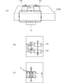
- 5(A), 5(B), and 5(C) are diagrams showing the mounting structure of the switching elements Q1, Q2 and the input capacitor Ci particularly to the substrate of the switching power supply device according to the second embodiment. be.
- FIG. 6 is a circuit diagram of a switching power supply device 103A according to the third embodiment.
- FIG. 7 is a circuit diagram of another switching power supply device 103B according to the third embodiment.
- FIG. 1 is a circuit diagram of a switching power supply device 101 according to the first embodiment.
- the switching power supply device 101 includes a circuit board provided with input sections Pin1 and Pin2 for DC input power, output sections Pout1 and Pout2 for DC power, a DC-DC converter 2, and a noise reduction circuit 1.
- FIG. 1 is a circuit diagram of a switching power supply device 101 according to the first embodiment.
- the switching power supply device 101 includes a circuit board provided with input sections Pin1 and Pin2 for DC input power, output sections Pout1 and Pout2 for DC power, a DC-DC converter 2, and a noise reduction circuit 1.
- FIG. 1 is a circuit diagram of a switching power supply device 101 according to the first embodiment.
- the switching power supply device 101 includes a circuit board provided with input sections Pin1 and Pin2 for DC input power, output sections Pout1 and Pout2 for DC power, a DC-DC converter 2, and a noise reduction circuit 1.
- FIG. 1 is a circuit diagram of a switching power supply device 101 according to the first
- the DC-DC converter 2 includes an input capacitor Ci, a switching circuit including switching elements Q1 and Q2, capacitors C1 and C2, a smoothing coil SC, an isolation transformer TR, diodes D1 and D2, an output smoothing capacitor Co and a choke coil CC. It is
- the noise reduction circuit 1 is mounted on the circuit board and includes a surface-mounted common mode choke coil CMCC having two input terminals Ti1, Ti2 and two output terminals To1, To2.
- the two input terminals Ti1 and Ti2 of the common mode choke coil CMCC are electrically connected to the positive (Pin1) and negative (Pin2) of the input section through the first circuit patterns PP11 and PP12, respectively.
- An X capacitor Cx is provided between the first circuit patterns PP11 and PP12.
- Y capacitors Cy1 and Cy2 are provided between both ends of the input capacitor Ci and the frame ground FG.
- Two output terminals To1 and To2 of the common mode choke coil CMCC are electrically connected to two terminals of the input capacitor Ci through second circuit patterns PP21 and PP22, respectively.
- Two terminals of the input capacitor Ci are connected to two input terminals of the switching circuit by the switching elements Q1 and Q2 through the third circuit patterns CP1 and CP2, respectively.
- a smoothing coil SC is connected between the connection point of the switching elements Q1 and Q2 and one end of the primary winding of the isolation transformer TR. It is connected to two circuit patterns PP21 and PP22.
- Diodes D1 and D2 an output smoothing capacitor Co and a choke coil CC are connected to the secondary winding of the insulating transformer TR.
- the DC input power supply PS is, for example, a lithium ion battery, for example, a high voltage battery of about several hundred volts (about 200 V to 600 V), and the DC voltage is input to the input parts Pin1 and Pin2.
- Switching elements Q1 and Q2 are controlled by a control signal from a switching control circuit, and switching element Q1 and switching element Q2 are alternately turned on/off.
- the output voltage of the switching circuit by the switching elements Q1 and Q2 is applied to the primary winding of the isolation transformer TR, and the output current of the switching circuit flows through the primary winding of the isolation transformer TR.
- Diodes D1 and D2 rectify the output current of the secondary winding of isolation transformer TR.
- Diodes D1 and D2 are examples of rectifying elements according to the present invention.
- the output smoothing capacitor Co smoothes the voltage rectified by the diodes D1 and D2.
- the choke coil CC smoothes the current flowing between the output smoothing capacitor Co and the output sections Pout1 and Pout2.
- the load Lo is, for example, a lead-acid battery, such as a low-voltage battery of about 12V.
- the circuit board has a plurality of current paths through which switching currents flow due to the switching operation of the switching circuit.
- the switching elements Q1, Q2 and the input capacitor Ci form a current loop including third circuit patterns CP1, CP2.
- the path lengths of the second circuit patterns PP21 and PP22 are longer than the path lengths of the third circuit patterns CP1 and CP2. Further, among the plurality of current paths, the path lengths of the third circuit patterns CP1 and CP2 are the shortest compared to the path lengths of the other current paths.
- the X capacitor Cx is a parasitic capacitance that occurs when the first circuit patterns PP11 and PP12 face each other in parallel, and corresponds to the "first parasitic capacitance” according to the present invention.
- the Y capacitors Cy1 and Cy2 are parasitic capacitances generated by the second circuit patterns PP21 and PP22 facing each other in parallel, and correspond to "second parasitic capacitances" according to the present invention.
- the X capacitor Cx, the common mode choke coil CMCC, and the Y capacitors Cy1 and Cy2 form a CLC ⁇ -type low-pass filter, and this low-pass filter reduces noise.
- the second parasitic capacitance reduces common mode noise.
- the Y capacitors Cy1, Cy2 and the frame ground FG are directly connected, but the Y capacitors Cy1, Cy2 and the frame ground FG are electrically connected through a capacitive element or an impedance element. good too. As a result, an effective noise reduction effect applied to the material and structure of the frame ground FG can be obtained.
- the DC input power supply PS is connected to other electronic devices that receive power from the DC input power supply PS and operate at a high voltage.
- Other electronic devices are, for example, inverters and motors.
- the load Lo is a low-voltage battery and receives power from this low-voltage battery or from the switching power supply device 101 .
- Other electronic devices are, for example, car navigation systems and wireless communication devices that operate at the low voltage.
- the circuit board has a plurality of current paths through which switching currents flow due to the switching operation of the switching circuit.
- the path lengths of the second circuit patterns PP21 and PP22 are longer than the path lengths of the third circuit patterns CP1 and CP2.
- the path lengths of the third circuit patterns CP1 and CP2 are the shortest compared to the path lengths of the other current paths.
- FIG. 2 is a diagram showing paths of noise currents flowing through the switching power supply device 101 according to the first embodiment.
- the DC input power supply PS is connected to another electronic device 201 that receives power from the DC input power supply PS.
- Other electronic devices 201 are, for example, inverters and motors that operate at high voltage.
- the load Lo is a low-voltage battery, and another electronic device 202 that receives power from this low-voltage battery or from the switching power supply device 101 is connected.
- Other electronic equipment 202 is, for example, a car navigation system or a wireless communication device that operates at the low voltage.
- the switching power supply device 101 is provided in a metal housing that is electrically connected to the frame ground FG.
- the ground pattern of the circuit board that constitutes the switching power supply device 101 is electrically connected to the frame ground FG through the metal housing. That is, the negative electrode Pout2 of the output section of the switching power supply device 101 is connected to the metal housing.
- a parasitic capacitance Cs1 is formed between the other electronic device 201 and the frame ground FG, and a parasitic capacitance Cs2 is formed between the switching elements Q1, Q2 and the metal casing.
- the other electronic devices 201 are inverters and motors, which are mounted on the frame ground FG in an electrically insulated state and a thermally conductive state through an insulator sheet.
- a parasitic capacitance Cs1 is generated in the portion interposing the insulator sheet.
- the switching elements Q1 and Q2 are thermally coupled to the metal housing through the insulator sheet in order to dissipate the generated heat to the metal housing and frame ground FG.
- the above-mentioned parasitic capacitance Cs2 is generated in the portion where the insulator sheet is interposed.
- the common mode noise current from the switching elements Q1 and Q2, which are noise sources passes through the parasitic capacitance Cs2 and the frame ground FG to the Y capacitor Cy1. , Cy2.
- noise currents do not reach the input units Pin1 and Pin2, and electromagnetic interference with other electronic devices 201 is prevented.
- the common mode choke coil CMCC is provided between the X capacitor Cx and the Y capacitors Cy1 and Cy2, the X capacitor Cx, the common mode choke coil CMCC, and the Y capacitors Cy1 and Cy2 form a low-pass filter against common mode noise. , and the noise current to the electronic device 201 is suppressed by this low-pass filter.
- Y capacitors Cy1 and Cy2 are electrically connected between the common mode choke coil CMCC and the input capacitor Ci.
- the common mode choke coil CMCC and the Y capacitors Cy1 and Cy2 constitute two low-pass filters, and the noise reduction effect is great.
- a switching circuit composed of switching elements Q1 and Q2 is arranged on one main surface of the multilayer circuit board, and an input capacitor Ci is arranged on the other main surface of the multilayer circuit board (second embodiment, FIG. 5A). , FIG. 5(B), FIG. 5(C)).
- the plane of the current loop flowing in the input capacitor Ci and the switching circuit is non-parallel to the current path flowing in other circuit parts of the multilayer circuit, and the input capacitor Ci is a connecting portion of one end of the switching circuit on the multilayer circuit board. and the connecting portion at the other end, for example, through one or more through-hole conductors.
- connection point of the Y capacitors Cy1 and Cy2 is electrically connected to the frame ground FG.
- the effect of reducing the common mode noise current is high.
- it may be electrically connected to the frame ground through a capacitive element or an impedance element.
- the negative electrode (Pout2) of the DC power output units Pout1 and Pout2 has the same potential as the frame ground FG of the housing of the switching power supply device 101 . This stabilizes the operation of the "feedback control circuit (not shown)" that detects the output voltage and controls the switching operations of the switching elements Q1 and Q2 to stabilize the output voltage at a predetermined value. , the noise reduction effect is high.
- the noise reduction circuit 1 is located between the DC input power supply PS and the input capacitor Ci, and arranged linearly between the input parts Pin1, Pin2 and the DC-DC converter 2 on the circuit board ( Second embodiment, see FIG. 4). In this configuration, a large noise reduction effect can be achieved by the action of reducing jumping of noise due to electromagnetic interference in a plurality of electronic components constituting a circuit.
- the noise reduction circuit 1 has positive and negative patterns sufficiently larger than component mounting lands for mounting the common mode choke coil. As a result, heat dissipation in the common mode choke coil is high.
- the metal housing is provided and is connected so as to have the same potential as the frame ground FG, so the noise reduction effect is high.
- the noise balance circuit formed by the noise reduction circuit 1 using a circuit board cancels and balances the common mode noise generated by the switching operations of the switching elements Q1 and Q2, thereby enhancing the noise reduction effect. can.
- FIG. 3 is a perspective view of a common mode choke coil.
- FIG. 4 is a perspective view showing the configuration on the circuit board of the switching power supply.
- the common mode choke coil CMCC has a rectangular parallelepiped shape, and has four terminals Ti1, Ti2, To1, and To2 formed on its lower surface.
- This common mode choke coil CMCC includes a ring-shaped magnetic core and a toroidal coil made of a conductor wound around the magnetic core inside a resin case.
- the circuit board PWB is provided with connectors for input portions Pin1 and Pin2 of the DC input power supply, an X capacitor Cx, a common mode choke coil CMCC, Y capacitors Cy1 and Cy2, and a DC-DC converter 2. .
- the positive terminal (Pin1) of the input section, the positive terminal of the input capacitor Ci, the negative terminal (Pin2) of the input section and the negative terminal of the input capacitor Ci are connected to a plurality of conductor layers of the circuit board PWB through a plurality of through-hole conductors.
- the circuit configuration of this switching power supply is as shown in the first embodiment. With this configuration, heat dissipation is high and conductor loss can be reduced.
- FIG. 5A is a side perspective view of the circuit board PWB on which the input capacitor Ci and the switching elements Q1 and Q2 are mounted.
- FIG. 5B is a plan view of the circuit board PWB, and
- FIG. 5C is a bottom view of the circuit board PWB.
- the input capacitor Ci is composed of three chip capacitors connected in parallel, each mounted on the lower surface of the circuit board PWB.
- the switching elements Q1 and Q2 are mounted on the upper surface of the circuit board PWB.
- the input capacitor Ci and the switching elements Q1 and Q2 are positioned to overlap each other when the circuit board PWB is viewed from above.
- arrows conceptually indicate paths of current flowing through connection loops composed of the input capacitor Ci and the switching elements Q1 and Q2.
- the switching elements Q1 and Q2 are mounted on one main surface of the circuit board PWB, and the input capacitor Ci is mounted on the other main surface of the circuit board PWB.
- Q2 overlaps at least a part of the circuit board PWB in plan view, so that the surface of the current loop flowing through the input capacitor Ci and the switching circuit becomes the current path flowing through the circuit section formed on the other main surface of the circuit board PWB. non-parallel.
- the input capacitor Ci is directly connected to the connection portion of one end and the connection portion of the other end of the switching circuit on the circuit board PWB so as to be the shortest, the input capacitor Ci and the switching elements Q1 and Q2 The path of the current flowing through the connection loop becomes extremely short.
- the loop surface of the connection loop composed of the input capacitor Ci and the switching elements Q1 and Q2 faces the surface direction (lateral side) of the circuit board PWB, other components mounted on the circuit board PWB Magnetic field coupling with parts is difficult. Therefore, there is almost no noise propagation or radiation due to unnecessary coupling.
- the input capacitor Ci does not necessarily have to be mounted on the surface of the circuit board.
- the circuit board PWB may be composed of a multi-layer board and the input capacitor Ci may be formed in this multi-layer board.
- the third embodiment will exemplify a switching power supply device in which the configuration between the input section and the switching circuit is different from the example shown in the first embodiment.
- FIG. 6 is a circuit diagram of a switching power supply device 103A according to the third embodiment.
- the switching power supply device 103A includes a circuit board on which input sections Pin1 and Pin2 of a DC input power supply, output sections Pout1 and Pout2 of DC power, a DC-DC converter 2, and a noise reduction circuit 1 are provided.
- the switching power supply 103A differs from the switching power supply 101 shown in FIG. 1 in that a second common mode choke coil CMCC2 is provided between the Y capacitors Cy1, Cy2 and the input capacitor Ci. This second common mode choke coil CMCC2 is part of the noise reduction circuit.
- one of the first common mode choke coil CMCC1 and the second common mode choke coil CMCC2 has a self-resonance frequency of 0.53 MHz or more and 1.8 MHz or less, and the other self-resonance frequency is 76 MHz or more and 108 MHz or less.
- the AM radio broadcast frequency band (0.53 MHz to 1.8 MHz) and the FM radio broadcast frequency band (76 MHz to 108 MHz) to the other electronic device 201 connected to the DC input power supply PS can effectively suppress the propagation of the noise current of the electronic device 201 to reduce electromagnetic interference with other electronic devices 201 .
- FIG. 7 is a circuit diagram of another switching power supply device 103B according to the third embodiment.
- the switching power supply device 103B similarly to the switching power supply device 103A shown in FIG. Between Cx, the X capacitor Cx and the input capacitor Ci, between the positive terminals of the input sections Pin1 and Pin2 and the metal housing and the frame ground FG, and between the negative terminals of the input sections Pin1 and Pin2 and the metal housing and the frame ground FG. Y capacitors Cy1 and Cy2 are respectively connected between .
- a switching power supply device 103B shown in FIG. 7 includes a second common mode choke coil CMCC2 between the Y capacitors Cy1, Cy2 and the first common mode choke coil CMCC1.
- CMCC1 and the second common mode choke coil CMCC2 has a self-resonant frequency of 0.53 MHz or more and 1.8 MHz or less, and the other self-resonant frequency of 76 MHz or more and 108 MHz or less. Even with such a configuration, propagation of noise current to other electronic devices 201 connected to the DC input power supply PS can be effectively suppressed, and electromagnetic interference with other electronic devices 201 can be reduced.
- the rectifying elements for rectifying the output of the isolation transformer TR are composed of the diodes D1 and D2, but the rectifying elements are composed of synchronous rectifying elements switched in synchronization with the switching elements Q1 and Q2. good too.
- loss in the rectifying element can be reduced.
- the switching power supply device 101 is a DC-DC converter mounted on an electric vehicle, loss in the DC-DC converter can be reduced.
- 1 and 2 illustrate the switching power supply device including the step-down DC-DC converter 2, but the switching power supply device including a step-up DC-DC converter and a step-up/step-down DC-DC converter are also applicable.
- the invention is equally applicable.
- 1, 2 and the like illustrate the switching power supply device including the isolated DC-DC converter 2 including the isolation transformer TR, but the present invention also applies to the switching power supply device including the non-insulated DC-DC converter. is equally applicable.
Landscapes
- Engineering & Computer Science (AREA)
- Power Engineering (AREA)
- Physics & Mathematics (AREA)
- Electromagnetism (AREA)
- Dc-Dc Converters (AREA)
Priority Applications (2)
| Application Number | Priority Date | Filing Date | Title |
|---|---|---|---|
| JP2023539720A JP7582488B2 (ja) | 2021-08-02 | 2022-07-05 | スイッチング電源装置 |
| US18/403,297 US12609615B2 (en) | 2021-08-02 | 2024-01-03 | Switching power supply device for reducing common mode noise generated by a switching element |
Applications Claiming Priority (2)
| Application Number | Priority Date | Filing Date | Title |
|---|---|---|---|
| JP2021126369 | 2021-08-02 | ||
| JP2021-126369 | 2021-08-02 |
Related Child Applications (1)
| Application Number | Title | Priority Date | Filing Date |
|---|---|---|---|
| US18/403,297 Continuation US12609615B2 (en) | 2021-08-02 | 2024-01-03 | Switching power supply device for reducing common mode noise generated by a switching element |
Publications (1)
| Publication Number | Publication Date |
|---|---|
| WO2023013343A1 true WO2023013343A1 (ja) | 2023-02-09 |
Family
ID=85155835
Family Applications (1)
| Application Number | Title | Priority Date | Filing Date |
|---|---|---|---|
| PCT/JP2022/026657 Ceased WO2023013343A1 (ja) | 2021-08-02 | 2022-07-05 | スイッチング電源装置 |
Country Status (3)
| Country | Link |
|---|---|
| US (1) | US12609615B2 (https=) |
| JP (1) | JP7582488B2 (https=) |
| WO (1) | WO2023013343A1 (https=) |
Cited By (1)
| Publication number | Priority date | Publication date | Assignee | Title |
|---|---|---|---|---|
| JP2024145976A (ja) * | 2023-03-31 | 2024-10-15 | ダイキン工業株式会社 | 電力変換装置、空気調和機 |
Families Citing this family (1)
| Publication number | Priority date | Publication date | Assignee | Title |
|---|---|---|---|---|
| CN115360919B (zh) * | 2021-04-30 | 2026-01-16 | 台达电子工业股份有限公司 | 功率转换装置 |
Citations (4)
| Publication number | Priority date | Publication date | Assignee | Title |
|---|---|---|---|---|
| WO2016147492A1 (ja) * | 2015-03-16 | 2016-09-22 | 三菱電機株式会社 | 電力用回路装置 |
| JP2017184328A (ja) * | 2016-03-28 | 2017-10-05 | 株式会社豊田自動織機 | 車載インバータ装置及び車載流体機械 |
| WO2020202797A1 (ja) * | 2019-04-04 | 2020-10-08 | 住友電気工業株式会社 | チョークコイル |
| JP6851554B1 (ja) * | 2020-04-20 | 2021-03-31 | 三菱電機株式会社 | 電力変換装置および空気調和機 |
Family Cites Families (6)
| Publication number | Priority date | Publication date | Assignee | Title |
|---|---|---|---|---|
| JP5765591B2 (ja) * | 2013-04-18 | 2015-08-19 | 株式会社デンソー | 電源装置 |
| WO2019130874A1 (ja) * | 2017-12-27 | 2019-07-04 | 株式会社村田製作所 | 電源装置 |
| WO2022138216A1 (ja) * | 2020-12-21 | 2022-06-30 | 株式会社村田製作所 | スイッチング電源装置 |
| WO2022138215A1 (ja) * | 2020-12-21 | 2022-06-30 | 株式会社村田製作所 | スイッチング電源装置 |
| JP7563598B2 (ja) * | 2021-06-30 | 2024-10-08 | 株式会社村田製作所 | スイッチング電源装置 |
| JP2025043930A (ja) * | 2023-09-19 | 2025-04-01 | 株式会社村田製作所 | スイッチング電源装置 |
-
2022
- 2022-07-05 WO PCT/JP2022/026657 patent/WO2023013343A1/ja not_active Ceased
- 2022-07-05 JP JP2023539720A patent/JP7582488B2/ja active Active
-
2024
- 2024-01-03 US US18/403,297 patent/US12609615B2/en active Active
Patent Citations (4)
| Publication number | Priority date | Publication date | Assignee | Title |
|---|---|---|---|---|
| WO2016147492A1 (ja) * | 2015-03-16 | 2016-09-22 | 三菱電機株式会社 | 電力用回路装置 |
| JP2017184328A (ja) * | 2016-03-28 | 2017-10-05 | 株式会社豊田自動織機 | 車載インバータ装置及び車載流体機械 |
| WO2020202797A1 (ja) * | 2019-04-04 | 2020-10-08 | 住友電気工業株式会社 | チョークコイル |
| JP6851554B1 (ja) * | 2020-04-20 | 2021-03-31 | 三菱電機株式会社 | 電力変換装置および空気調和機 |
Cited By (2)
| Publication number | Priority date | Publication date | Assignee | Title |
|---|---|---|---|---|
| JP2024145976A (ja) * | 2023-03-31 | 2024-10-15 | ダイキン工業株式会社 | 電力変換装置、空気調和機 |
| JP7846383B2 (ja) | 2023-03-31 | 2026-04-15 | ダイキン工業株式会社 | 電力変換装置、空気調和機 |
Also Published As
| Publication number | Publication date |
|---|---|
| US12609615B2 (en) | 2026-04-21 |
| JP7582488B2 (ja) | 2024-11-13 |
| US20240136926A1 (en) | 2024-04-25 |
| JPWO2023013343A1 (https=) | 2023-02-09 |
| US20240235395A9 (en) | 2024-07-11 |
Similar Documents
| Publication | Publication Date | Title |
|---|---|---|
| US10491180B2 (en) | Board-type noise filter and electronic device | |
| US10297379B2 (en) | Integrated transformers and coupled inductors and associated systems and methods | |
| US9263177B1 (en) | Pin inductors and associated systems and methods | |
| CN110310815A (zh) | 平面变压器、电源转换电路以及适配器 | |
| JP7563598B2 (ja) | スイッチング電源装置 | |
| US12609615B2 (en) | Switching power supply device for reducing common mode noise generated by a switching element | |
| CN108235672B (zh) | 屏蔽体、电子电路以及dc-dc转换器 | |
| US11164696B2 (en) | Low common mode noise transformer structure with external float wire mount | |
| CN117253700A (zh) | 变压器 | |
| WO2016143207A1 (ja) | ノイズフィルタ | |
| JPWO2019220626A1 (ja) | ノイズフィルタ | |
| JP7563599B2 (ja) | スイッチング電源装置 | |
| WO2018089313A1 (en) | Low common mode noise transformer structure with external float wire mount | |
| JP3823322B2 (ja) | 分布定数構造 | |
| WO2022219925A1 (ja) | フィルタ装置及び電力変換装置 | |
| US20250266207A1 (en) | Electrical assemblies including magnetic devices | |
| JP2017169431A (ja) | 電源装置 | |
| US20250292970A1 (en) | Capacitive winding of a dc link capacitor and dc link capacitor with a common-mode current leakage function | |
| US20250203799A1 (en) | Integrated power supply using a planar energy transfer element | |
| US11990886B2 (en) | Filter unit | |
| US20250392212A1 (en) | Switching power supply | |
| JP3181441B2 (ja) | 薄型電源装置 | |
| WO2026014107A1 (ja) | スイッチング電源装置 | |
| JPS631593Y2 (https=) |
Legal Events
| Date | Code | Title | Description |
|---|---|---|---|
| 121 | Ep: the epo has been informed by wipo that ep was designated in this application |
Ref document number: 22852769 Country of ref document: EP Kind code of ref document: A1 |
|
| WWE | Wipo information: entry into national phase |
Ref document number: 2023539720 Country of ref document: JP |
|
| NENP | Non-entry into the national phase |
Ref country code: DE |
|
| 122 | Ep: pct application non-entry in european phase |
Ref document number: 22852769 Country of ref document: EP Kind code of ref document: A1 |