WO2023007923A1 - Multilayer ceramic capacitor, circuit module and method for producing circuit module - Google Patents
Multilayer ceramic capacitor, circuit module and method for producing circuit module Download PDFInfo
- Publication number
- WO2023007923A1 WO2023007923A1 PCT/JP2022/021066 JP2022021066W WO2023007923A1 WO 2023007923 A1 WO2023007923 A1 WO 2023007923A1 JP 2022021066 W JP2022021066 W JP 2022021066W WO 2023007923 A1 WO2023007923 A1 WO 2023007923A1
- Authority
- WO
- WIPO (PCT)
- Prior art keywords
- internal electrode
- ceramic capacitor
- electrode layers
- section
- capacitor
- Prior art date
Links
- 239000003985 ceramic capacitor Substances 0.000 title claims abstract description 113
- 238000004519 manufacturing process Methods 0.000 title claims description 14
- 239000003990 capacitor Substances 0.000 claims abstract description 79
- 229910010293 ceramic material Inorganic materials 0.000 claims abstract description 4
- 239000011347 resin Substances 0.000 claims description 24
- 229920005989 resin Polymers 0.000 claims description 24
- 229910052751 metal Inorganic materials 0.000 claims description 21
- 239000002184 metal Substances 0.000 claims description 21
- 238000007747 plating Methods 0.000 claims description 15
- 238000005498 polishing Methods 0.000 claims description 13
- 238000000034 method Methods 0.000 claims description 10
- 230000003746 surface roughness Effects 0.000 claims description 8
- 230000003247 decreasing effect Effects 0.000 abstract 1
- 239000010410 layer Substances 0.000 description 279
- 239000004020 conductor Substances 0.000 description 41
- 238000000605 extraction Methods 0.000 description 14
- 230000004048 modification Effects 0.000 description 9
- 238000012986 modification Methods 0.000 description 9
- 238000010304 firing Methods 0.000 description 8
- 239000000463 material Substances 0.000 description 6
- 229910000679 solder Inorganic materials 0.000 description 6
- 150000001875 compounds Chemical class 0.000 description 5
- 238000005452 bending Methods 0.000 description 4
- 239000000919 ceramic Substances 0.000 description 4
- 239000011521 glass Substances 0.000 description 4
- 150000002739 metals Chemical class 0.000 description 4
- 229910001252 Pd alloy Inorganic materials 0.000 description 3
- 229910045601 alloy Inorganic materials 0.000 description 3
- 239000000956 alloy Substances 0.000 description 3
- 229910052763 palladium Inorganic materials 0.000 description 3
- 239000002245 particle Substances 0.000 description 3
- 229910052709 silver Inorganic materials 0.000 description 3
- 239000011230 binding agent Substances 0.000 description 2
- 229910052802 copper Inorganic materials 0.000 description 2
- 238000003475 lamination Methods 0.000 description 2
- 229910052759 nickel Inorganic materials 0.000 description 2
- 239000011241 protective layer Substances 0.000 description 2
- 239000002904 solvent Substances 0.000 description 2
- 229920001187 thermosetting polymer Polymers 0.000 description 2
- 239000010409 thin film Substances 0.000 description 2
- 229910002367 SrTiO Inorganic materials 0.000 description 1
- 239000005388 borosilicate glass Substances 0.000 description 1
- 238000000576 coating method Methods 0.000 description 1
- 238000010586 diagram Methods 0.000 description 1
- 238000006073 displacement reaction Methods 0.000 description 1
- 229910052737 gold Inorganic materials 0.000 description 1
- 238000007646 gravure printing Methods 0.000 description 1
- 238000000462 isostatic pressing Methods 0.000 description 1
- 239000002923 metal particle Substances 0.000 description 1
- 239000000203 mixture Substances 0.000 description 1
- 238000007639 printing Methods 0.000 description 1
- 238000007650 screen-printing Methods 0.000 description 1
- 239000004065 semiconductor Substances 0.000 description 1
- 238000005245 sintering Methods 0.000 description 1
- 238000004544 sputter deposition Methods 0.000 description 1
- 238000007740 vapor deposition Methods 0.000 description 1
Images


Classifications
-
- H—ELECTRICITY
- H01—ELECTRIC ELEMENTS
- H01G—CAPACITORS; CAPACITORS, RECTIFIERS, DETECTORS, SWITCHING DEVICES OR LIGHT-SENSITIVE DEVICES, OF THE ELECTROLYTIC TYPE
- H01G2/00—Details of capacitors not covered by a single one of groups H01G4/00-H01G11/00
- H01G2/02—Mountings
- H01G2/06—Mountings specially adapted for mounting on a printed-circuit support
-
- H—ELECTRICITY
- H01—ELECTRIC ELEMENTS
- H01G—CAPACITORS; CAPACITORS, RECTIFIERS, DETECTORS, SWITCHING DEVICES OR LIGHT-SENSITIVE DEVICES, OF THE ELECTROLYTIC TYPE
- H01G2/00—Details of capacitors not covered by a single one of groups H01G4/00-H01G11/00
- H01G2/10—Housing; Encapsulation
-
- H—ELECTRICITY
- H01—ELECTRIC ELEMENTS
- H01G—CAPACITORS; CAPACITORS, RECTIFIERS, DETECTORS, SWITCHING DEVICES OR LIGHT-SENSITIVE DEVICES, OF THE ELECTROLYTIC TYPE
- H01G4/00—Fixed capacitors; Processes of their manufacture
- H01G4/002—Details
- H01G4/005—Electrodes
- H01G4/012—Form of non-self-supporting electrodes
-
- H—ELECTRICITY
- H01—ELECTRIC ELEMENTS
- H01G—CAPACITORS; CAPACITORS, RECTIFIERS, DETECTORS, SWITCHING DEVICES OR LIGHT-SENSITIVE DEVICES, OF THE ELECTROLYTIC TYPE
- H01G4/00—Fixed capacitors; Processes of their manufacture
- H01G4/002—Details
- H01G4/224—Housing; Encapsulation
-
- H—ELECTRICITY
- H01—ELECTRIC ELEMENTS
- H01G—CAPACITORS; CAPACITORS, RECTIFIERS, DETECTORS, SWITCHING DEVICES OR LIGHT-SENSITIVE DEVICES, OF THE ELECTROLYTIC TYPE
- H01G4/00—Fixed capacitors; Processes of their manufacture
- H01G4/002—Details
- H01G4/228—Terminals
- H01G4/232—Terminals electrically connecting two or more layers of a stacked or rolled capacitor
- H01G4/2325—Terminals electrically connecting two or more layers of a stacked or rolled capacitor characterised by the material of the terminals
-
- H—ELECTRICITY
- H01—ELECTRIC ELEMENTS
- H01G—CAPACITORS; CAPACITORS, RECTIFIERS, DETECTORS, SWITCHING DEVICES OR LIGHT-SENSITIVE DEVICES, OF THE ELECTROLYTIC TYPE
- H01G4/00—Fixed capacitors; Processes of their manufacture
- H01G4/30—Stacked capacitors
-
- H—ELECTRICITY
- H01—ELECTRIC ELEMENTS
- H01G—CAPACITORS; CAPACITORS, RECTIFIERS, DETECTORS, SWITCHING DEVICES OR LIGHT-SENSITIVE DEVICES, OF THE ELECTROLYTIC TYPE
- H01G4/00—Fixed capacitors; Processes of their manufacture
- H01G4/38—Multiple capacitors, i.e. structural combinations of fixed capacitors
-
- H—ELECTRICITY
- H01—ELECTRIC ELEMENTS
- H01G—CAPACITORS; CAPACITORS, RECTIFIERS, DETECTORS, SWITCHING DEVICES OR LIGHT-SENSITIVE DEVICES, OF THE ELECTROLYTIC TYPE
- H01G4/00—Fixed capacitors; Processes of their manufacture
- H01G4/40—Structural combinations of fixed capacitors with other electric elements, the structure mainly consisting of a capacitor, e.g. RC combinations
-
- H—ELECTRICITY
- H01—ELECTRIC ELEMENTS
- H01L—SEMICONDUCTOR DEVICES NOT COVERED BY CLASS H10
- H01L25/00—Assemblies consisting of a plurality of individual semiconductor or other solid state devices ; Multistep manufacturing processes thereof
- H01L25/03—Assemblies consisting of a plurality of individual semiconductor or other solid state devices ; Multistep manufacturing processes thereof all the devices being of a type provided for in the same subgroup of groups H01L27/00 - H01L33/00, or in a single subclass of H10K, H10N, e.g. assemblies of rectifier diodes
- H01L25/04—Assemblies consisting of a plurality of individual semiconductor or other solid state devices ; Multistep manufacturing processes thereof all the devices being of a type provided for in the same subgroup of groups H01L27/00 - H01L33/00, or in a single subclass of H10K, H10N, e.g. assemblies of rectifier diodes the devices not having separate containers
-
- H—ELECTRICITY
- H01—ELECTRIC ELEMENTS
- H01L—SEMICONDUCTOR DEVICES NOT COVERED BY CLASS H10
- H01L25/00—Assemblies consisting of a plurality of individual semiconductor or other solid state devices ; Multistep manufacturing processes thereof
- H01L25/18—Assemblies consisting of a plurality of individual semiconductor or other solid state devices ; Multistep manufacturing processes thereof the devices being of types provided for in two or more different subgroups of the same main group of groups H01L27/00 - H01L33/00, or in a single subclass of H10K, H10N
-
- H—ELECTRICITY
- H05—ELECTRIC TECHNIQUES NOT OTHERWISE PROVIDED FOR
- H05K—PRINTED CIRCUITS; CASINGS OR CONSTRUCTIONAL DETAILS OF ELECTRIC APPARATUS; MANUFACTURE OF ASSEMBLAGES OF ELECTRICAL COMPONENTS
- H05K1/00—Printed circuits
- H05K1/18—Printed circuits structurally associated with non-printed electric components
- H05K1/181—Printed circuits structurally associated with non-printed electric components associated with surface mounted components
-
- H—ELECTRICITY
- H05—ELECTRIC TECHNIQUES NOT OTHERWISE PROVIDED FOR
- H05K—PRINTED CIRCUITS; CASINGS OR CONSTRUCTIONAL DETAILS OF ELECTRIC APPARATUS; MANUFACTURE OF ASSEMBLAGES OF ELECTRICAL COMPONENTS
- H05K2201/00—Indexing scheme relating to printed circuits covered by H05K1/00
- H05K2201/10—Details of components or other objects attached to or integrated in a printed circuit board
- H05K2201/10007—Types of components
- H05K2201/10015—Non-printed capacitor
Definitions
- the present invention relates to a multilayer ceramic capacitor, a circuit module using the same, and a method for manufacturing the circuit module.
- Patent Document 1 discloses a multilayer ceramic capacitor.
- Such a multilayer ceramic capacitor includes a laminate in which a plurality of dielectric layers containing a ceramic material and a plurality of internal electrode layers are laminated, and external electrodes provided on end surfaces of the laminate.
- a laminated ceramic capacitor according to the present invention is a laminated body in which a plurality of dielectric layers containing a ceramic material and a plurality of internal electrode layers are laminated, wherein two main surfaces facing each other in the thickness direction and the thickness a laminate having two side surfaces facing each other in a width direction that intersects the direction and two end surfaces that face each other in a length direction that intersects with the thickness direction and the width direction; and the two main surfaces of the laminate. and two external electrode pairs respectively arranged at .
- the stacked body includes a first capacitance section including a part of the internal electrode layers among the plurality of internal electrode layers, wherein adjacent internal electrode layers of the part of the internal electrode layers face each other; and a second capacitive section including other internal electrode layers other than the one of the plurality of internal electrode layers, and in which adjacent internal electrode layers of the other internal electrode layers face each other.
- the partial internal electrode layer in the first capacitor section is connected to one of the two external electrode pairs, and the other internal electrode layer in the second capacitor section. are connected to the other of the two external electrode pairs.
- a circuit module according to the present invention is a circuit module in which electronic circuit components are mounted on a circuit board, comprising: the circuit board; the above laminated ceramic capacitor that is the electronic circuit component mounted on the circuit board; and a resin mold member disposed around the laminated ceramic capacitor.
- the laminated ceramic capacitor is formed of either one of the first capacitor portion and the second capacitor portion by removing a portion in the thickness direction, and resin is disposed around the laminated ceramic capacitor.
- the surface roughness of the main surface of the laminated ceramic capacitor on the side opposite to the circuit board is greater than the surface roughness of the laminated body of the laminated ceramic capacitor facing the mold member.
- a circuit module manufacturing method is the circuit module manufacturing method described above, wherein the multilayer ceramic capacitor, which is the electronic circuit component, is mounted on the circuit board, and the periphery of the multilayer ceramic capacitor is covered with the resin. It is filled with a mold member, and the laminated ceramic capacitor and the resin mold member are polished from the thickness direction.
- the present invention it is possible to provide a multilayer ceramic capacitor that can be made thinner when mounted in a circuit module without reducing the bending strength of the component. Further, according to the present invention, it is possible to provide a circuit module that can be made thinner by using the multilayer ceramic capacitor, and a method for manufacturing the circuit module.
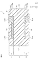
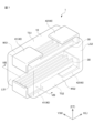
- FIG. 1 is a perspective view showing a laminated ceramic capacitor according to this embodiment
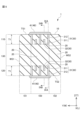
- FIG. FIG. 2 is a sectional view taken along the line II-II of the multilayer ceramic capacitor shown in FIG. 1
- FIG. 3 is a cross-sectional view taken along line IIIA-IIIA of the multilayer ceramic capacitor shown in FIG. 2
- FIG. 3 is a cross-sectional view taken along line IIIB-IIIB of the multilayer ceramic capacitor shown in FIG. 2
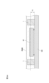
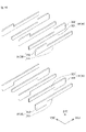
- 4 is a perspective view showing internal electrode layers in the multilayer ceramic capacitor shown in FIGS. 1 to 3B
- FIG. It is a sectional view showing an example of a circuit module concerning this embodiment.
- FIG. 5B is a side view showing the laminated ceramic capacitor after polishing in the circuit module shown in FIG. 5A;
- FIG. 5B is a side view showing the laminated ceramic capacitor after polishing in the circuit module shown in FIG. 5A;
- FIG. 5B is a side view showing the laminated ceramic capacitor after polishing in the circuit module shown in FIG
- FIG. 9 is a cross-sectional view taken along line IXA-IXA of the multilayer ceramic capacitor shown in FIG. 8;
- FIG. 9 is a cross-sectional view taken along line IXB-IXB of the multilayer ceramic capacitor shown in FIG. 8;
- FIG. 10 is a perspective view showing internal electrode layers in the multilayer ceramic capacitor shown in FIGS. 7 to 9B;
- FIG. 10 is a perspective view showing a laminated ceramic capacitor according to a modification of the embodiment;
- 12 is a cross-sectional view of the multilayer ceramic capacitor shown in FIG. 11 taken along line XII-XII;
- FIG. 12 is a cross-sectional view taken along line XIII-XIII of the multilayer ceramic capacitor shown in FIG. 11;
- FIG. FIG. 14 is a perspective view showing internal electrode layers in the multilayer ceramic capacitor shown in FIGS. 11 to 13;
- FIG. 1 is a perspective view showing a laminated ceramic capacitor according to this embodiment
- FIG. 2 is a cross-sectional view taken along the line II-II of the laminated ceramic capacitor shown in FIG. 3A is a sectional view taken along line IIIA-IIIA of the laminated ceramic capacitor shown in FIG. 2
- FIG. 3B is a sectional view taken along line IIIB-IIIB of the laminated ceramic capacitor shown in FIG.
- a laminated ceramic capacitor 1 shown in FIGS. 1 to 3B includes a laminated body 10 and two external electrode pairs 40. As shown in FIG. Each external electrode pair 40 includes a first external electrode 41 and a second external electrode 42 .
- the X direction is the length direction L of the multilayer ceramic capacitor 1 and the multilayer body 10
- the Y direction is the width direction W of the multilayer ceramic capacitor 1 and the multilayer body 10
- the Z direction is the thickness of the multilayer ceramic capacitor 1 and the multilayer body 10.
- direction T. 2 is also referred to as the WT section
- the sections illustrated in FIGS. 3A and 3B are also referred to as the LT section. Note that the length direction L, the width direction W, and the thickness direction T are not necessarily orthogonal to each other, and may intersect each other.
- FIG. 4 is a perspective view showing internal electrode layers in the multilayer ceramic capacitor shown in FIGS. 1 to 3B, and FIG. 1 shows the internal electrode layers and one of the external electrode pairs shown in FIG. It is
- the laminate 10 has a substantially rectangular parallelepiped shape, and has a first main surface TS1 and a second main surface TS2 facing each other in the thickness direction T, and a first side surface WS1 and a second side surface WS2 facing each other in the width direction W. , and a first end face LS1 and a second end face LS2 facing each other in the length direction L.
- the corners and ridges of the laminate 10 are preferably rounded.
- a corner is a portion where three surfaces of the laminate 10 intersect, and a ridge is a portion where two surfaces of the laminate 10 intersect.
- the laminate 10 has multiple dielectric layers 20 and multiple internal electrode layers 30 stacked in the width direction W.
- the laminate 10 has an inner layer portion 100, and a first outer layer portion 101 and a second outer layer portion 102 arranged to sandwich the inner layer portion 100 in the width direction W, that is, the stacking direction.
- the laminate 10 has, in the thickness direction T, a first capacitive section 110, a second capacitive section 120, and a non-capacitive section .
- the first capacitive section 110 is arranged on the first main surface TS1 side of the laminate 10
- the second capacitive section 120 is arranged on the second main surface TS2 side of the laminate 10.
- the non-capacitive section 130 is located between the first capacitive section 110 and the second capacitive section 120 .
- the inner layer section 100 includes a portion of the multiple dielectric layers 20 and multiple internal electrode layers 30 . More specifically, the first capacitor section 110 in the internal layer section 100 includes a portion of the multiple dielectric layers 20 and a portion of the multiple internal electrode layers 30 .
- the second capacitive section 120 in the inner layer section 100 includes a portion of the plurality of dielectric layers 20 and a portion of the plurality of internal electrode layers 30 other than the portion for the first capacitive section 110 . In the first capacitor section 110 and the second capacitor section 120, adjacent internal electrode layers 30 are arranged to face each other with the dielectric layer 20 interposed therebetween.
- the first capacitive section 110 and the second capacitive section 120 are portions that generate capacitance and substantially function as capacitors.
- the non-capacitance portion 130 in the internal layer portion 100 does not include the internal electrode layers 30 but includes a plurality of dielectric layers 20 .
- the first outer layer portion 101 is arranged on the first side surface WS1 side of the laminate 10, and the second outer layer portion 102 is arranged on the second side surface WS2 side of the laminate 10. More specifically, the first outer layer portion 101 is arranged between the internal electrode layer 30 closest to the first side surface WS1 among the plurality of internal electrode layers 30 and the first side surface WS1.
- the second outer layer portion 102 is arranged between the internal electrode layer 30 closest to the second side surface WS2 among the plurality of internal electrode layers 30 and the second side surface WS2.
- the first outer layer portion 101 and the second outer layer portion 102 do not include the internal electrode layer 30, and include portions of the plurality of dielectric layers 20 other than the portion for the inner layer portion 100, respectively.
- the first outer layer portion 101 and the second outer layer portion 102 are portions that function as protective layers for the first capacitor portion 110 and the second capacitor portion 120 in the inner layer portion 100 .
- the material of the dielectric layer 20 for example, a dielectric ceramic containing BaTiO 3 , CaTiO 3 , SrTiO 3 , CaZrO 3 or the like as a main component can be used. Moreover, as a material of the dielectric layer 20, a Mn compound, an Fe compound, a Cr compound, a Co compound, a Ni compound, or the like may be added as an accessory component.
- the thickness of the dielectric layer 20 is not particularly limited, it is preferably 0.4 ⁇ m or more and 2.0 ⁇ m or less, for example.
- the number of dielectric layers 20 is not particularly limited, but is preferably 50 or more and 450 or less, for example.
- the number of dielectric layers 20 is the total number of dielectric layers in the inner layer portion and the number of dielectric layers in the outer layer portion.
- each of the first capacitor section 110 and the second capacitor section 120 includes a plurality of first internal electrode layers 31 and a plurality of second electrode layers 30 as the plurality of internal electrode layers 30.
- An internal electrode layer 32 is included.
- the first internal electrode layer 31 includes a counter electrode portion 311 and a lead electrode portion 312
- the second internal electrode layer 32 includes a counter electrode portion 321 and a lead electrode portion 322 .
- the counter electrode section 311 and the counter electrode section 321 are opposed to each other with the dielectric layer 20 interposed therebetween in the lamination direction of the laminate 10 , that is, in the width direction W.
- the shape of the counter electrode portion 311 and the counter electrode portion 321 is not particularly limited, and may be, for example, a substantially rectangular shape.
- the counter electrode portion 311 and the counter electrode portion 321 are portions that generate capacitance and substantially function as capacitors.
- the extraction electrode section 312 extends from a portion of the counter electrode section 311 on the first end surface LS1 side of the laminate 10 toward the first main surface TS1 of the laminate 10, It is exposed on the first main surface TS1.
- the extraction electrode portion 322 extends from a portion of the counter electrode portion 321 on the second end surface LS2 side of the laminate 10 toward the first main surface TS1 of the laminate 10 and is exposed at the first main surface TS1. are doing.
- the shape of the extraction electrode portion 312 and the extraction electrode portion 322 is not particularly limited, and may be, for example, a substantially rectangular shape.
- the first internal electrode layer 31 is connected to the first external electrode 41 in the external electrode pair 40 arranged on the first main surface TS1 of the laminate 10, It is spaced apart from the second external electrode 42 in the external electrode pair 40 arranged on the first main surface TS1.
- the second internal electrode layer 32 is connected to the second external electrode 42 in the external electrode pair 40 arranged on the first main surface TS1 of the laminate 10 and arranged on the first main surface TS1. It is separated from the first external electrode 41 in the external electrode pair 40 .
- the counter electrode section 311 and the counter electrode section 321 are opposed to each other in the stacking direction of the laminate 10, that is, in the width direction W, with the dielectric layer 20 interposed therebetween.
- the extraction electrode section 312 extends from the portion of the counter electrode section 311 on the first end surface LS1 side of the laminate 10 toward the second main surface TS2 of the laminate 10, It is exposed at the second main surface TS2.
- the extraction electrode portion 322 extends from a portion of the counter electrode portion 321 on the second end surface LS2 side of the laminate 10 toward the second main surface TS2 of the laminate 10 and is exposed at the second main surface TS2. are doing.
- the first internal electrode layer 31 is connected to the first external electrode 41 in the external electrode pair 40 arranged on the second main surface TS2 of the laminate 10, It is separated from the second external electrode 42 in the external electrode pair 40 arranged on the second main surface TS2.
- the second internal electrode layer 32 is connected to the second external electrode 42 in the external electrode pair 40 arranged on the second main surface TS2 of the laminate 10, and is arranged on the second main surface TS2. It is separated from the first external electrode 41 in the external electrode pair 40 .
- the plurality of internal electrode layers 30 in the first capacitor section 110 and the plurality of internal electrode layers 30 in the second capacitor section 120 may be plane-symmetrical with respect to the center in the thickness direction T.
- the plurality of internal electrode layers 30 in the first capacitor section 110 and the plurality of internal electrode layers 30 in the second capacitor section 120 are arranged with respect to the center in the thickness direction T and the center in the width direction W. , may be rotationally symmetric.
- the plurality of internal electrode layers 30 in the first capacitor portion 110 and the second The plurality of internal electrode layers 30 in the capacitor section 120 may be rotationally symmetrical with respect to the center of the laminate 10 in the thickness direction T and the center of the inner layer section 100 of the laminate 10 in the width direction W. .
- the thickness T1 in the thickness direction T of the internal electrode layer 30 in the first capacitor section 110 in other words, the thickness T1 from the first main surface TS1 of the internal electrode layer 30 in the first capacitor section 110 is 25 ⁇ m. It is preferable in it being more than 70 micrometers or less. Further, the thickness T1 in the thickness direction T of the internal electrode layer 30 in the second capacitor section 120, in other words, the thickness T1 from the second main surface TS2 of the internal electrode layer 30 in the second capacitor section 120 is , 25 ⁇ m or more and 70 ⁇ m or less.
- the first internal electrode layer 31 and the second internal electrode layer 32 contain metal Ni as a main component.
- the first internal electrode layer 31 and the second internal electrode layer 32 are formed of metals such as Cu, Ag, Pd, or Au, or alloys containing at least one of these metals, such as Ag—Pd alloys. , may be included as a main component, or may be included as a component other than the main component.
- the first internal electrode layer 31 and the second internal electrode layer 32 may contain dielectric particles having the same composition as the ceramic contained in the dielectric layer 20 as a component other than the main component.
- the metal of the main component is defined as the metal component with the highest weight percentage.
- the thickness of the first internal electrode layer 31 and the second internal electrode layer 32 is not particularly limited, it is preferably 0.2 ⁇ m or more and 1.0 ⁇ m or less, for example.
- the number of the first internal electrode layers 31 and the second internal electrode layers 32 is not particularly limited, but is preferably 2 or more and 430 or less, for example.
- the thickness in the thickness direction T is preferably 0.1 mm or more and 0.3 mm or less.
- One external electrode pair 40 of the two external electrode pairs 40 is arranged on the first main surface TS1 of the laminate 10, and the other external electrode pair 40 of the two external electrode pairs 40 is arranged on the laminate 10 is arranged on the second main surface TS2.
- Each external electrode pair 40 includes a first external electrode 41 and a second external electrode 42 .
- the first external electrode 41 in one external electrode pair 40 is arranged on the first end surface LS1 side of the first main surface TS1 of the laminate 10, and the second external electrode in one external electrode pair 40 42 is arranged on the first main surface TS1 of the laminate 10 on the second end surface LS2 side.
- the first external electrode 41 is connected to the first internal electrode layer 31 in the first capacitor section 110
- the second external electrode 42 is connected to the second internal electrode layer 32 in the first capacitor section 110 . It is connected to the.
- the first external electrode 41 in the other external electrode pair 40 is arranged on the first end surface LS1 side of the second main surface TS2 of the laminate 10, and the second external electrode in the other external electrode pair 40 42 is arranged on the second main surface TS2 of the laminate 10 on the second end surface LS2 side.
- the first external electrode 41 is connected to the first internal electrode layer 31 in the second capacitor section 120
- the second external electrode 42 is connected to the second internal electrode layer 32 in the second capacitor section 120 . It is connected to the.
- the first external electrode 41 and the second external electrode 42 are preferably plated metal layers. That is, it is preferable that the first external electrode 41 and the second external electrode 42 be metal layers containing only plating layers.
- the metal layer made of plating includes, for example, at least one selected from metals such as Cu, Ni, Ag, Pd, and Au, and alloys such as Ag—Pd alloys.
- the metal layer made of plating may be formed of multiple layers. A three-layer structure of Cu plating, Ni plating and Sn plating is preferred.
- the Ni plating layer can prevent the base electrode layer from being eroded by solder when mounting the ceramic electronic component, and the Sn plating layer improves the wettability of the solder when mounting the ceramic electronic component. , can be easily implemented.
- the thickness of each plated metal layer is not particularly limited, and may be 1 ⁇ m or more and 10 ⁇ m or less.
- first external electrode 41 and the second external electrode 42 may have a base layer of a metal layer made of plating.
- the underlayer may be a thin film layer of 1 ⁇ m or less formed by a thin film forming method such as a sputtering method or a vapor deposition method and having metal particles deposited thereon.
- the thickness of the entire first external electrode 41 and second external electrode 42 is preferably 4 ⁇ m or more and 16 ⁇ m or less.
- the base layer may be a fired layer containing metal and glass.
- glass include glass components containing at least one selected from B, Si, Ba, Mg, Al, Li, and the like.
- borosilicate glass can be used.
- the metal contains Cu as a main component.
- the metal may contain at least one selected from metals such as Ni, Ag, Pd, or Au, or alloys such as Ag—Pd alloys as a main component, or may contain as a component other than the main component. It's okay.
- the sintered layer is a layer obtained by applying a conductive paste containing metal and glass to the laminate by a dip method and then sintering it.
- the firing may be performed after firing the internal electrode layers, or may be performed simultaneously with the firing of the internal electrode layers. Also, the fired layer may be a plurality of layers.
- the base layer may be a resin layer containing conductive particles and a thermosetting resin.
- the resin layer may be formed on the fired layer described above, or may be formed directly on the laminate without forming the fired layer.
- the resin layer is a layer obtained by applying a conductive paste containing conductive particles and a thermosetting resin to the laminate by a coating method and firing the layer.
- the firing may be performed after firing the internal electrode layers, or may be performed simultaneously with the firing of the internal electrode layers.
- the resin layer may be a plurality of layers.
- each base layer as a fired layer or resin layer is not particularly limited, and may be 1 ⁇ m or more and 10 ⁇ m or less.
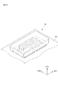
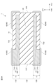
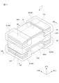
- FIG. 5A is a cross-sectional view showing an example of a circuit module according to this embodiment.
- 5B is a side view showing the laminated ceramic capacitor after polishing in the circuit module shown in FIG. 5A
- FIG. 5C is a perspective view showing the laminated ceramic capacitor after polishing in the circuit module shown in FIG. 5A.
- the polished surfaces After polishing, the polished surfaces have greater surface roughness than the side surfaces WS1 and WS2 and the end surfaces LS1 and LS2. Note that the surface roughness RA is measured by a laser displacement meter or the like.
- the circuit module 500 includes a circuit board CB, electronic circuit components, and a resin mold member RMM.
- a laminated ceramic capacitor 1A and an integrated circuit IC are illustrated as electronic circuit components, but the present invention is not limited to these, and various electronic circuit components can be applied.
- electronic circuit components may include capacitors, inductors, resistors, semiconductor ICs (switch ICs, LNA ICs, controller ICs, PA ICs, etc.), filters (SAW, BAW, LC filters, etc.), etc. .
- Electronic circuit components such as a multilayer ceramic capacitor 1A and an integrated circuit IC are mounted on one main surface of the circuit board CB.
- the surroundings of the laminated ceramic capacitor 1A and the integrated circuit IC are filled with a resin mold member RMM.
- the resin mold member RMM is arranged around the laminated ceramic capacitor 1A and the integrated circuit IC.
- Electronic circuit components may also be mounted on the other main surface of the circuit board CB.
- the laminated ceramic capacitor 1A and the integrated circuit IC are polished and removed after being molded with the resin mold member RMM.
- the main surface of the multilayer ceramic capacitor 1A opposite to the circuit board CB and the main surface of the resin mold member RMM opposite to the circuit board CB are aligned in the thickness direction T.
- the surface roughness (polished surface) of the main surface of the multilayer ceramic capacitor 1A on the side opposite to the circuit board CB was greater than the surface roughness (side surfaces WS1 and WS2 and end surfaces LS1 and LS2).
- the multilayer ceramic capacitor 1A is a mode in which the above-described multilayer ceramic capacitor 1 is polished from the thickness direction T, and part of the thickness direction T is removed. More specifically, laminated ceramic capacitor 1A consists of either one of first capacitive section 110 and second capacitive section 120 in laminated ceramic capacitor 1 described above. That is, the multilayer ceramic capacitor 1A has the other of the first capacitance section 110 and the second capacitance section 120 in the above-described multilayer ceramic capacitor 1 removed, and the first capacitance section 110 and the second capacitance section 120 are Contains only one.
- a ridgeline portion where the main surfaces TS1 and TS2 of the laminate 10 intersect with the end surfaces LS1 and LS2, and a ridgeline portion where the main surfaces TS1 and TS2 and the side surfaces WS1 and WS2 of the laminate 10 intersect, that is, chamfered ridgeline portions , is, for example, 10 ⁇ m or more and 35 ⁇ m or less.
- a thickness T2 of the multilayer ceramic capacitor 1A from the circuit board CB is preferably 29 ⁇ m or more and 86 ⁇ m or less.
- Dielectric sheet for the dielectric layers 20 and a conductive paste for the internal electrode layers 30 are prepared.
- Dielectric sheets and conductive pastes contain binders and solvents. Known materials can be used as the binder and solvent.
- an internal electrode pattern is formed on the dielectric sheet by printing a conductive paste on the dielectric sheet, for example, in a predetermined pattern.
- a method for forming the internal electrode pattern screen printing, gravure printing, or the like can be used.
- a predetermined number of dielectric sheets for the second outer layer portion 102 on which the internal electrode pattern is not printed are laminated.
- Dielectric sheets for the inner layer section 100 on which the internal electrode pattern is printed are successively laminated thereon.
- a predetermined number of dielectric sheets for the first outer layer section 101 on which the internal electrode pattern is not printed are laminated thereon. Thereby, a laminated sheet is produced.
- the laminated sheet is pressed in the lamination direction by means of isostatic pressing or the like to produce a laminated block.
- the laminated block is cut into a predetermined size to cut out laminated chips. At this time, the corners and ridges of the laminated chips are rounded by barrel polishing or the like.
- the laminated chip is fired to produce the laminated body 10 .
- the firing temperature is preferably 900° C. or more and 1400° C. or less, although it depends on the materials of the dielectric and internal electrodes.
- a metal layer consisting of plating is formed on the first main surface TS1 of the laminate 10 to form one external electrode pair 40 . Also, a metal layer consisting of plating is formed on the second main surface TS2 of the laminate 10 to form the other external electrode pair 40 .
- the laminated ceramic capacitor 1 described above is obtained.
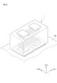
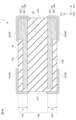
- FIG. 6A is a cross-sectional view showing the circuit module after polishing in the manufacturing process of the circuit module shown in FIG. 5A.
- 6B is a side view showing the unpolished laminated ceramic capacitor in the unpolished circuit module shown in FIG. 6A
- FIG. 6C is a perspective showing the unpolished laminated ceramic capacitor in the unpolished circuit module shown in FIG. 6A. It is a diagram.
- the electronic circuit components such as the laminated ceramic capacitor 1, the integrated circuit IC, and the resin mold member RMM are polished from the thickness direction T. At this time, the exposed surface of the electronic circuit component may be remolded.
- circuit components may be mounted on the other main surface of the circuit board CB, or the periphery of the electronic circuit components may be filled with a resin mold member. Thereby, the circuit module 500 shown in FIG. 5A is obtained.
- the two capacitive sections 110 and 120 and the two external electrode pairs 40 respectively corresponding to the two capacitive sections 110 and 120 are provided. More specifically, according to the multilayer ceramic capacitor 1 of this embodiment, the two capacitive sections 110 and 120 are provided in the thickness direction T. As shown in FIG. Thus, by polishing and removing one capacitor in the thickness direction T, a thin capacitor can be obtained by using the other capacitor. In this way, the bending strength of the part before polishing is not reduced. On the other hand, when mounting a circuit module, it can be made thinner by polishing in the thickness direction T. FIG.
- the external electrode pair 40 is a metal layer made of plating, in other words, if the baked layer or the resin layer is not included, further reduction in thickness is possible. .
- the internal electrode layers 30 in the first capacitor section 110 and the internal electrode layers 30 in the second capacitor section 120 are arranged in planes with respect to the center in the thickness direction T. Symmetrical or rotationally symmetrical. This eliminates the need to distinguish between the front and back sides of the multilayer ceramic capacitor 1 .
- the present invention is not limited to the above-described embodiments, and various modifications and variations are possible.
- the multilayer ceramic capacitor 1 in which the two external electrode pairs 40 are arranged on each of the first principal surface TS1 and the second principal surface TS2 of the multilayer body 10 is exemplified.
- the shape of the external electrode pair 40 is not limited to this, and the external electrode pair 40 may extend from the main surface TS1 or TS2 to the end surface LS1 or LS2 (see Modification 1 below).
- the external electrode pair 40 may extend from the main surface TS1 or TS2 to the side surface WS1 or WS2 (see modification 2 below).
- FIG. 7 is a perspective view showing a laminated ceramic capacitor according to a modification of this embodiment
- FIG. 8 is a cross-sectional view taken along line VIII-VIII of the laminated ceramic capacitor shown in FIG. 9A is a cross-sectional view taken along line IXA-IXA of the laminated ceramic capacitor shown in FIG. 8
- FIG. 7 shows the internal electrode layers and one of the external electrode pairs shown in FIG. It is
- the multilayer ceramic capacitor 1 shown in FIGS. and the shape of the internal electrode layer 30 in the second capacitor section 120 is different.
- the first external electrode 41 in one external electrode pair 40 arranged on the first main surface TS1 of the laminate 10 extends from the first main surface TS1 to part of the first end surface LS1.
- the second external electrode 42 in one external electrode pair 40 may extend from the first main surface TS1 to a portion of the second end surface LS2.
- the first external electrode 41 in the other external electrode pair 40 arranged on the second main surface TS2 of the laminate 10 extends from the second main surface TS2 to a part of the first end surface LS1.
- the second external electrode 42 in the other external electrode pair 40 may extend from the second main surface TS2 to a portion of the second end surface LS2.
- the first internal electrode layer 31 extends from the portion of the counter electrode section 311 on the side of the first end surface LS1 of the multilayer body 10 . also extends toward the first end face LS1 of and is exposed at the first end face LS1 as well.
- the first internal electrode layer 31 and the first external electrode 41 are connected not only to the first main surface TS1, but also to the first end surface LS1, and to the first main surface TS1 and the first end surface LS1. are also connected at the ridges where Therefore, the contact area between the first internal electrode layer 31 and the first external electrode 41 can be increased, and the contact resistance between the first internal electrode layer 31 and the first external electrode 41 can be reduced. can.
- the second internal electrode layer 32 extends from the portion of the counter electrode section 321 on the side of the second end surface LS2 of the laminate 10. It also extends towards the second end face LS2 of the body 10 and is exposed there as well.
- the second internal electrode layer 32 and the second external electrode 42 are connected not only to the first main surface TS1, but also to the second end surface LS2, and to the first main surface TS1 and the second end surface LS2. are also connected at the ridges of the laminate 10 where the . Therefore, the contact area between the second internal electrode layer 32 and the second external electrode 42 can be increased, and the contact resistance between the second internal electrode layer 32 and the second external electrode 42 can be reduced. can.
- the first internal electrode layer 31, more specifically the extraction electrode section 312 extends from the portion of the counter electrode section 311 on the first end surface LS1 side of the laminate 10 to It also extends toward the first end surface LS1 of the laminate 10 and is exposed at the first end surface LS1 as well. Accordingly, the first internal electrode layer 31 and the first external electrode 41 are connected not only to the second main surface TS2 but also to the first end surface LS1 and the second main surface TS2 and the first end surface LS1. are also connected at the ridges of the laminate 10 where the . Therefore, the contact area between the first internal electrode layer 31 and the first external electrode 41 can be increased, and the contact resistance between the first internal electrode layer 31 and the first external electrode 41 can be reduced. can.
- the second internal electrode layer 32 extends from the portion of the counter electrode portion 321 on the side of the second end surface LS2 of the laminate 10 to the second end surface LS2 of the laminate 10. , and is also exposed at the second end surface LS2.
- the second internal electrode layer 32 and the second external electrode 42 are connected not only to the second main surface TS2, but also to the second end surface LS2, and to the second main surface TS2 and the second end surface LS2. are also connected at the ridges of the laminate 10 where the . Therefore, the contact area between the second internal electrode layer 32 and the second external electrode 42 can be increased, and the contact resistance between the second internal electrode layer 32 and the second external electrode 42 can be reduced. can.
- the corners of the first internal electrode layers 31 are preferably rounded along the ridgeline where the main surface TS1 or TS2 of the laminate 10 intersects with the end surface LS1. is preferably rounded along the ridge line where the main surface TS1 or TS2 of the laminate 10 intersects with the end surface LS2.
- Modification 2 11 is a perspective view showing a laminated ceramic capacitor according to a modification of the present embodiment
- FIG. 12 is a sectional view taken along line XII-XII of the laminated ceramic capacitor shown in FIG. 11, and
- FIG. 2 is a cross-sectional view taken along line XIII-XIII of the multilayer ceramic capacitor shown
- 14 is a perspective view showing internal electrode layers in the multilayer ceramic capacitor shown in FIGS. 11 to 13, and FIG. 11 shows the internal electrode layers and one of the external electrode pairs shown in FIG. It is
- the laminated ceramic capacitor 1 shown in FIGS. 11 to 13 differs from the laminated ceramic capacitor 1 shown in FIGS. 1 to 3B in the shape of the two external electrode pairs 40 and the shape of the laminate 10.
- the first external electrode 41 in one of the external electrode pairs 40 arranged on the first main surface TS1 of the laminate 10 extends from the first main surface TS1 to part of the first end surface LS1. , to part of the first side WS1 and part of the second side WS2. Further, the second external electrode 42 in one external electrode pair 40 extends from the first main surface TS1 to part of the second end surface LS2, part of the first side surface WS1, and part of the second side surface WS2. It may extend to the part. As a result, the wettability of solder can be used to improve the bonding strength when mounting on a circuit board.
- the first external electrode 41 in the other external electrode pair 40 arranged on the second main surface TS2 of the laminate 10 extends from the second main surface TS2 to part of the first end surface LS1, It may extend as far as part of one side WS1 and part of the second side WS2.
- the second external electrode 42 in the other external electrode pair 40 extends from the second principal surface TS2 to part of the second end surface LS2, part of the first side surface WS1, and part of the second side surface WS2. It may extend to the part.
- the wettability of solder can be used to improve the bonding strength when mounting on a circuit board.
- the internal electrode layers and the external electrode layers can be connected at the end surfaces and side surfaces of the laminate. Therefore, the layered body may have the thickness direction as the layering direction.
- the laminate 10 may have a plurality of dielectric layers 20 and a plurality of internal electrode layers 30 laminated in the thickness direction T.
- the laminate 10 has an inner layer portion 100 and a first outer layer portion 101 and a second outer layer portion 102 arranged to sandwich the inner layer portion 100 in the thickness direction T, that is, the stacking direction.
- the laminate 10 has, in the thickness direction T, a first capacitive section 110, a second capacitive section 120, and a non-capacitative section 130, similarly to the above-described embodiments.
- the inner layer section 100 includes a portion of the multiple dielectric layers 20 and the multiple internal electrode layers 30 . More specifically, the first capacitor section 110 in the internal layer section 100 includes a portion of the multiple dielectric layers 20 and a portion of the multiple internal electrode layers 30 .
- the second capacitive section 120 in the inner layer section 100 includes a portion of the plurality of dielectric layers 20 and a portion of the plurality of internal electrode layers 30 other than the portion for the first capacitive section 110 . In the first capacitor section 110 and the second capacitor section 120, adjacent internal electrode layers 30 are arranged to face each other with the dielectric layer 20 interposed therebetween.
- the first capacitive section 110 and the second capacitive section 120 are portions that generate capacitance and substantially function as capacitors.
- the non-capacitance portion 130 in the inner layer portion 100 does not include the internal electrode layers 30 but includes a plurality of dielectric layers 20 .
- the first outer layer portion 101 is arranged on the first main surface TS1 side of the laminate 10, and the second outer layer portion 102 is arranged on the second main surface TS2 side of the laminate 10. More specifically, the first outer layer portion 101 is arranged between the internal electrode layer 30 closest to the first main surface TS1 among the plurality of internal electrode layers 30 and the first main surface TS1. , the second outer layer portion 102 is arranged between the internal electrode layer 30 closest to the second main surface TS2 among the plurality of internal electrode layers 30 and the second main surface TS2.
- the first outer layer portion 101 and the second outer layer portion 102 do not include the internal electrode layer 30, and include portions of the plurality of dielectric layers 20 other than the portion for the inner layer portion 100, respectively.
- the first outer layer portion 101 and the second outer layer portion 102 are portions that function as protective layers for the first capacitor portion 110 and the second capacitor portion 120 in the inner layer portion 100 .
- each of the first capacitor section 110 and the second capacitor section 120 includes a plurality of first internal electrode layers 31 and a plurality of second electrode layers 30 as the plurality of internal electrode layers 30.
- An internal electrode layer 32 is included.
- the first internal electrode layer 31 includes a counter electrode portion 311 and a lead electrode portion 312
- the second internal electrode layer 32 includes a counter electrode portion 321 and a lead electrode portion 322 .
- the counter electrode section 311 and the counter electrode section 321 face each other with the dielectric layer 20 interposed therebetween in the stacking direction of the laminate 10, that is, the thickness direction T.
- the counter electrode portion 311 and the counter electrode portion 321 are portions that generate capacitance and substantially function as capacitors.
- the extraction electrode section 312 extends from the first end surface LS1 of the multilayer body 10, the first side surface WS1 and the first side surface WS1 of the multilayer body 10 from the portion of the counter electrode section 311 on the side of the first end surface LS1 of the multilayer body 10. 2 side surface WS2 and exposed at the first end surface LS1, the first side surface WS1 and the second side surface WS2.
- the extraction electrode portion 322 extends from a portion of the counter electrode portion 321 on the second end surface LS2 side of the laminate 10 toward the second end surface LS2, the first side surface WS1 and the second side surface WS2 of the laminate 10. and exposed at the second end surface LS2, the first side surface WS1 and the second side surface WS2.
- the first internal electrode layer 31 includes the first external electrode 41 in the external electrode pair 40 arranged on the first main surface TS1 of the laminate 10, and the first The end surface LS1, the first side surface WS1, the second side surface WS2, and the edge portions of the laminate 10 where the end surface LS1 and the side surfaces WS1 and WS2 intersect are connected.
- the second internal electrode layer 32 includes the second external electrode 42 in the external electrode pair 40 arranged on the first main surface TS1 of the laminate 10, the second end surface LS2, the first side surface WS1, The second side surface WS2 and the edge line of the laminate 10 where the end surface LS2 and the side surfaces WS1 and WS2 intersect are connected.
- the extraction electrode section 312 extends from the portion of the counter electrode section 311 on the side of the first end surface LS1 of the multilayer body 10 to the first end surface LS1 of the multilayer body 10 and the first side surface. It extends toward WS1 and the second side surface WS2 and is exposed at the first end surface LS1, the first side surface WS1 and the second side surface WS2.
- the extraction electrode portion 322 extends from a portion of the counter electrode portion 321 on the second end surface LS2 side of the laminate 10 toward the second end surface LS2, the first side surface WS1 and the second side surface WS2 of the laminate 10. and exposed at the second end face LS2, the first side face WS1 and the second side face WS2.
- the first internal electrode layer 31 includes the first external electrode 41 in the external electrode pair 40 arranged on the second main surface TS2 of the laminate 10, and the first The end surface LS1, the first side surface WS1, the second side surface WS2, and the edge portions of the laminate 10 where the end surface LS1 and the side surfaces WS1 and WS2 intersect are connected.
- the second internal electrode layer 32 includes the second external electrode 42 in the external electrode pair 40 arranged on the second main surface TS2 of the laminate 10, the second end surface LS2, the first side surface WS1, The second side surface WS2 and the edge line of the laminate 10 where the end surface LS2 and the side surfaces WS1 and WS2 intersect are connected.
- the corners of the first internal electrode layers 31 are preferably rounded along the ridges where the end surface LS1 of the laminate 10 and the side surfaces WS1 and WS2 intersect.
- the corners are preferably rounded along the ridgeline where the end face LS2 of the laminate 10 and the side face WS1 or WS2 intersect.
- the plurality of internal electrode layers 30 in the first capacitor section 110 and the plurality of internal electrode layers 30 in the second capacitor section 120 may be plane-symmetrical with respect to the center in the thickness direction T.
- the plurality of internal electrode layers 30 in the first capacitor section 110 and the plurality of internal electrode layers 30 in the second capacitor section 120 are arranged with respect to the center in the thickness direction T and the center in the width direction W. , may be rotationally symmetric.
- the plurality of internal electrode layers 30 in the first capacitor portion 110 and the second The plurality of internal electrode layers 30 in the capacitor section 120 may be plane-symmetrical with respect to the center of the thickness direction T of the inner layer section 100 of the laminate 10, or the thickness of the inner layer section 100 of the laminate 10 may be symmetrical. It may be rotationally symmetrical with respect to the center in the length direction T and the center in the width direction W of the laminate 10 .
- the thickness T1 in the thickness direction T of the internal electrode layer 30 in the first capacitor section 110 in other words, the thickness T1 from the first main surface TS1 of the internal electrode layer 30 in the first capacitor section 110 is 25 ⁇ m. It is preferable in it being more than 70 micrometers or less. Further, the thickness T1 in the thickness direction T of the internal electrode layer 30 in the second capacitor section 120, in other words, the thickness T1 from the second main surface TS2 of the internal electrode layer 30 in the second capacitor section 120 is , 25 ⁇ m or more and 70 ⁇ m or less.
- the thickness of the first internal electrode layer 31 and the second internal electrode layer 32 is not particularly limited, it is preferably 0.4 ⁇ m or more and 2.0 ⁇ m or less, for example.
- the number of the first internal electrode layers 31 and the second internal electrode layers 32 is not particularly limited, but is preferably 2 or more and 35 or less, for example.
- first outer layer portion 101 and the second outer layer portion 102 may include a plurality of conductor portions 50 .
- the multiple conductor portions 50 have first conductor portions 511 and 512 and second conductor portions 521 and 522 .
- the first conductor portion 511 is arranged on the first end surface LS1 side of the first outer layer portion 101, and the first conductor portion 512 is arranged on the second end surface LS2 side of the first outer layer portion 101. It is The second conductor portion 521 is arranged on the first end surface LS1 side of the second outer layer portion 102, and the second conductor portion 522 is arranged on the second end surface LS2 side of the second outer layer portion 102. are placed in
- Each of the first conductor portions 511 and 512 and the second conductor portions 521 and 522 has a plurality of conductor layers 50M.
- the shape of the conductor layer 50M is not particularly limited as long as it is substantially rectangular, for example.
- a plurality of conductor layers 50M are stacked in the thickness direction T, that is, in the stacking direction, with dielectric layers 20 interposed therebetween.
- the end of the conductor layer 50M of the first conductor portion 511 is exposed on the first end surface LS1, the first side surface WS1 and the second side surface WS2.
- the end portion of the conductor layer 50M of the first conductor portion 511 is connected to the first external electrode 41 in the external electrode pair 40 arranged on the first main surface TS1 of the laminate 10 and the first end surface LS1.
- the ends of the conductor layer 50M of the first conductor portion 512 are exposed to the second end surface LS2, the first side surface WS1 and the second side surface WS2.
- the end portion of the conductor layer 50M of the first conductor portion 512 is connected to the second external electrode 42 in the external electrode pair 40 arranged on the first main surface TS1 of the laminate 10 and the second end surface LS2. , the first side surface WS1, the second side surface WS2, and the edge portions of the laminate 10 where the end surface LS2 and the side surfaces WS1 and WS2 intersect with the second external electrode 42. As shown in FIG.
- the end portion of the conductor layer 50M of the second conductor portion 521 is exposed to the first end surface LS1, the first side surface WS1 and the second side surface WS2.
- the end portion of the conductor layer 50M of the second conductor portion 521 is connected to the first external electrode 41 in the external electrode pair 40 arranged on the second main surface TS2 of the laminate 10 and the first end surface LS1.
- the end of the conductor layer 50M of the second conductor portion 522 is exposed to the second end surface LS2, the first side surface WS1 and the second side surface WS2.
- the end portion of the conductor layer 50M of the second conductor portion 522 is connected to the second external electrode 42 in the external electrode pair 40 arranged on the second main surface TS2 of the laminate 10 and the second end surface LS2.
- the corners of the conductor layer 50M are rounded along the ridgeline where the end surface LS1 of the laminate 10 and the side surfaces WS1 and WS2 intersect, or along the ridgeline where the end surface LS2 of the laminate 10 and the side surface WS1 or WS2 intersect. It is preferable if it is attached.
- the material of the conductor layer 50M is not particularly limited, but includes the same material as the internal electrode layer 30, for example.
- the thickness of the plurality of conductor layers 50M is not particularly limited, it is preferably 0.2 ⁇ m or more and 1.0 ⁇ m or less, for example.
- the number of the plurality of conductor layers 50M is not particularly limited, but is preferably 2 or more and 30 or less.
- the conductor layer 50M serves as a plating growth starting point.
Abstract
Description
図1は、本実施形態に係る積層セラミックコンデンサを示す斜視図であり、図2は、図1に示す積層セラミックコンデンサのII-II線断面図である。図3Aは、図2に示す積層セラミックコンデンサのIIIA-IIIA線断面図であり、図3Bは、図2に示す積層セラミックコンデンサのIIIB-IIIB線断面図である。図1~図3Bに示す積層セラミックコンデンサ1は、積層体10と2つの外部電極対40とを備える。外部電極対40の各々は、第1の外部電極41と第2の外部電極42とを含む。 (multilayer ceramic capacitor)
FIG. 1 is a perspective view showing a laminated ceramic capacitor according to this embodiment, and FIG. 2 is a cross-sectional view taken along the line II-II of the laminated ceramic capacitor shown in FIG. 3A is a sectional view taken along line IIIA-IIIA of the laminated ceramic capacitor shown in FIG. 2, and FIG. 3B is a sectional view taken along line IIIB-IIIB of the laminated ceramic capacitor shown in FIG. A laminated
次に、上述した積層セラミックコンデンサ1を実装した回路モジュールについて説明する。図5Aは、本実施形態に係る回路モジュールの一例を示す断面図である。図5Bは、図5Aに示す回路モジュールにおける研磨後の積層セラミックコンデンサを示す側面図であり、図5Cは、図5Aに示す回路モジュールにおける研磨後の積層セラミックコンデンサを示す斜視図である。研磨後、研磨された面は、側面WS1およびWS2、および端面LS1およびLS2より表面粗さが大きい。なお、表面粗さRAはレーザー変位計などにより測定される。 (circuit module)
Next, a circuit module in which the laminated
次に、上述した積層セラミックコンデンサ1の製造方法について説明する。まず、誘電体層20用の誘電体シート、および内部電極層30用の導電性ペーストを準備する。誘電体シートおよび導電性ペーストには、バインダおよび溶剤が含まれる。バインダおよび溶剤としては公知の材料を用いることができる。 (Manufacturing method of multilayer ceramic capacitor)
Next, a method for manufacturing the laminated
次に、上述した回路モジュール500の製造方法について説明する。図6Aは、図5Aに示す回路モジュールの製造プロセスにおける研磨後の回路モジュールを示す断面図である。図6Bは、図6Aに示す研磨前の回路モジュールにおける研磨前の積層セラミックコンデンサを示す側面図であり、図6Cは、図6Aに示す研磨前の回路モジュールにおける研磨前の積層セラミックコンデンサを示す斜視図である。 (Manufacturing method of circuit module)
Next, a method for manufacturing the
これにより、図5Aに示す回路モジュール500が得られる。 After that, electronic circuit components may be mounted on the other main surface of the circuit board CB, or the periphery of the electronic circuit components may be filled with a resin mold member.
Thereby, the
図7は、本実施形態の変形例に係る積層セラミックコンデンサを示す斜視図であり、図8は、図7に示す積層セラミックコンデンサのVIII-VIII線断面図である。図9Aは、図8に示す積層セラミックコンデンサのIXA-IXA線断面図であり、図9Bは、図8に示す積層セラミックコンデンサのIXB-IXB線断面図である。また、図10は、図7~図9Bに示す積層セラミックコンデンサにおける内部電極層を示す斜視図であり、図7には、図10に示す内部電極層、および外部電極対の一方が透かして示されている。 (Modification 1)
FIG. 7 is a perspective view showing a laminated ceramic capacitor according to a modification of this embodiment, and FIG. 8 is a cross-sectional view taken along line VIII-VIII of the laminated ceramic capacitor shown in FIG. 9A is a cross-sectional view taken along line IXA-IXA of the laminated ceramic capacitor shown in FIG. 8, and FIG. 9B is a cross-sectional view taken along line IXB-IXB of the laminated ceramic capacitor shown in FIG. 10 is a perspective view showing internal electrode layers in the multilayer ceramic capacitor shown in FIGS. 7 to 9B, and FIG. 7 shows the internal electrode layers and one of the external electrode pairs shown in FIG. It is
図11は、本実施形態の変形例に係る積層セラミックコンデンサを示す斜視図であり、図12は、図11に示す積層セラミックコンデンサのXII-XII線断面図であり、図13は、図11に示す積層セラミックコンデンサのXIII-XIII線断面図である。また、図14は、図11~図13に示す積層セラミックコンデンサにおける内部電極層を示す斜視図であり、図11には、図14に示す内部電極層、および外部電極対の一方が透かして示されている。 (Modification 2)
11 is a perspective view showing a laminated ceramic capacitor according to a modification of the present embodiment, FIG. 12 is a sectional view taken along line XII-XII of the laminated ceramic capacitor shown in FIG. 11, and FIG. FIG. 2 is a cross-sectional view taken along line XIII-XIII of the multilayer ceramic capacitor shown; 14 is a perspective view showing internal electrode layers in the multilayer ceramic capacitor shown in FIGS. 11 to 13, and FIG. 11 shows the internal electrode layers and one of the external electrode pairs shown in FIG. It is
1A 研磨後の積層セラミックコンデンサ
10 積層体
20 誘電体層
30 内部電極層
31 第1の内部電極層
311 対向電極部
312 引出電極部
32 第2の内部電極層
321 対向電極部
322 引出電極部
40 外部電極対
41 第1の外部電極
42 第2の外部電極
50 導体部
511,512 第1の導体部
521,522 第2の導体部
50M 導体層
100 内層部
101 第1の外層部
102 第2の外層部
110 第1の容量部
120 第2の容量部
130 非容量部
500 回路モジュール
CB 回路基板
RMM 樹脂モールド部材
IC 集積回路
L 長さ方向
T 厚さ方向
W 幅方向
LS1 第1の端面
LS2 第2の端面
TS1 第1の主面
TS2 第2の主面
WS1 第1の側面
WS2 第2の側面 1 Laminated
Claims (7)
- セラミック材料を含む複数の誘電体層と複数の内部電極層とが積層された積層体であって、厚さ方向に相対する2つの主面と、前記厚さ方向に交差する幅方向に相対する2つの側面と、前記厚さ方向および前記幅方向に交差する長さ方向に相対する2つの端面とを有する積層体と、
前記積層体の前記2つの主面にそれぞれ配置された2つの外部電極対と、
を備え、
前記積層体は、
前記複数の内部電極層のうちの一部の内部電極層を含み、前記一部の内部電極層のうち隣り合う内部電極層が対向している第1の容量部と、
前記複数の内部電極層のうちの前記一部以外の他部の内部電極層を含み、前記他部の内部電極層のうち隣り合う内部電極層が対向している第2の容量部と、
を有し、
前記第1の容量部における前記一部の内部電極層は、前記2つの外部電極対のうちの一方の外部電極対に接続されており、
前記第2の容量部における前記他部の内部電極層は、前記2つの外部電極対のうちの他方の外部電極対に接続されている、
積層セラミックコンデンサ。 A laminated body in which a plurality of dielectric layers containing a ceramic material and a plurality of internal electrode layers are laminated, wherein two main surfaces facing each other in a thickness direction face each other in a width direction intersecting the thickness direction a laminate having two side surfaces and two end surfaces facing each other in a length direction intersecting the thickness direction and the width direction;
two external electrode pairs respectively arranged on the two main surfaces of the laminate;
with
The laminate is
a first capacitance section including some internal electrode layers among the plurality of internal electrode layers, wherein adjacent internal electrode layers among the some internal electrode layers face each other;
a second capacitive section including internal electrode layers other than the one portion of the plurality of internal electrode layers, wherein adjacent internal electrode layers among the internal electrode layers of the other portion face each other;
has
the part of the internal electrode layers in the first capacitor section is connected to one of the two external electrode pairs,
The other internal electrode layer in the second capacitor section is connected to the other external electrode pair of the two external electrode pairs,
Multilayer ceramic capacitor. - 前記2つの外部電極対は、めっきからなる金属層である、請求項1に記載の積層セラミックコンデンサ。 The multilayer ceramic capacitor according to claim 1, wherein the two external electrode pairs are metal layers made of plating.
- 前記第1の容量部における前記一部の内部電極層と前記第2の容量部における前記他部の内部電極層とは、前記厚さ方向の中央に対して面対称である、請求項1または2に記載の積層セラミックコンデンサ。 2. The part of the internal electrode layers in the first capacitor section and the other part of the internal electrode layers in the second capacitor section are plane-symmetrical with respect to the center in the thickness direction. 3. The multilayer ceramic capacitor according to 2.
- 前記第1の容量部における前記一部の内部電極層と前記第2の容量部における前記他部の内部電極層とは、前記厚さ方向の中央に対して回転対称である、請求項1または2に記載の積層セラミックコンデンサ。 2. The part of the internal electrode layers in the first capacitor section and the other part of the internal electrode layers in the second capacitor section are rotationally symmetrical with respect to the center in the thickness direction. 3. The multilayer ceramic capacitor according to 2.
- 前記第1の容量部における前記一部の内部電極層および前記第2の容量部における前記他部の内部電極層の前記厚さ方向の厚さは、25μm以上70μm以下である、請求項1~4のいずれか1項に記載の積層セラミックコンデンサ。 1. The thickness in the thickness direction of the one internal electrode layer in the first capacitor section and the other internal electrode layer in the second capacitor section is 25 μm or more and 70 μm or less. 5. The multilayer ceramic capacitor according to any one of 4.
- 回路基板に電子回路部品が実装された回路モジュールであって、
前記回路基板と、
前記回路基板に実装された前記電子回路部品である、請求項1~5のいずれか1項に記載の積層セラミックコンデンサと、
前記積層セラミックコンデンサの周囲に配置された樹脂モールド部材と、
を備え、
前記積層セラミックコンデンサは、前記厚さ方向の一部が除去されて、前記第1の容量部および前記第2の容量部のうちいずれか一方からなり、
前記積層セラミックコンデンサの周囲に配置された樹脂モールド部材と相対する前記積層セラミックコンデンサの積層体の表面粗さより、前記積層セラミックコンデンサの前記回路基板と反対側の主面の表面粗さが大きい、
回路モジュール。 A circuit module in which electronic circuit components are mounted on a circuit board,
the circuit board;
The multilayer ceramic capacitor according to any one of claims 1 to 5, which is the electronic circuit component mounted on the circuit board;
a resin mold member disposed around the laminated ceramic capacitor;
with
the laminated ceramic capacitor is formed of either one of the first capacitance portion and the second capacitance portion by removing a portion in the thickness direction,
The surface roughness of the main surface of the laminated ceramic capacitor on the side opposite to the circuit board is greater than the surface roughness of the laminated body of the laminated ceramic capacitor facing the resin mold member arranged around the laminated ceramic capacitor,
circuit module. - 請求項6に記載の回路モジュールの製造方法であって、
前記回路基板に、前記電子回路部品である前記積層セラミックコンデンサを実装し、
前記積層セラミックコンデンサの周囲を前記樹脂モールド部材で埋め、
前記積層セラミックコンデンサおよび前記樹脂モールド部材を、前記厚さ方向から研磨する、
回路モジュールの製造方法。 A method for manufacturing the circuit module according to claim 6,
mounting the laminated ceramic capacitor, which is the electronic circuit component, on the circuit board;
Filling the periphery of the laminated ceramic capacitor with the resin mold member,
polishing the laminated ceramic capacitor and the resin mold member from the thickness direction;
A method of manufacturing a circuit module.
Priority Applications (3)
| Application Number | Priority Date | Filing Date | Title |
|---|---|---|---|
| JP2023538297A JPWO2023007923A1 (en) | 2021-07-30 | 2022-05-23 | |
| CN202280047144.5A CN117730383A (en) | 2021-07-30 | 2022-05-23 | Multilayer ceramic capacitor, circuit module, and method for manufacturing circuit module |
| KR1020247002550A KR20240023441A (en) | 2021-07-30 | 2022-05-23 | Multilayer ceramic capacitor, circuit module, and method of manufacturing circuit module |
Applications Claiming Priority (2)
| Application Number | Priority Date | Filing Date | Title |
|---|---|---|---|
| JP2021125896 | 2021-07-30 | ||
| JP2021-125896 | 2021-07-30 |
Publications (1)
| Publication Number | Publication Date |
|---|---|
| WO2023007923A1 true WO2023007923A1 (en) | 2023-02-02 |
Family
ID=85086499
Family Applications (1)
| Application Number | Title | Priority Date | Filing Date |
|---|---|---|---|
| PCT/JP2022/021066 WO2023007923A1 (en) | 2021-07-30 | 2022-05-23 | Multilayer ceramic capacitor, circuit module and method for producing circuit module |
Country Status (4)
| Country | Link |
|---|---|
| JP (1) | JPWO2023007923A1 (en) |
| KR (1) | KR20240023441A (en) |
| CN (1) | CN117730383A (en) |
| WO (1) | WO2023007923A1 (en) |
Citations (4)
| Publication number | Priority date | Publication date | Assignee | Title |
|---|---|---|---|---|
| JP2001332654A (en) * | 2000-03-17 | 2001-11-30 | Matsushita Electric Ind Co Ltd | Module provided with built-in electric element and manufacturing method thereof |
| JP2002299496A (en) * | 2001-03-30 | 2002-10-11 | Fujitsu Ltd | Semiconductor device and its fabricating method |
| JP2010258070A (en) * | 2009-04-22 | 2010-11-11 | Murata Mfg Co Ltd | Multilayer ceramic electronic component |
| JP2015053469A (en) * | 2013-08-07 | 2015-03-19 | 日東電工株式会社 | Method for manufacturing semiconductor package |
Family Cites Families (1)
| Publication number | Priority date | Publication date | Assignee | Title |
|---|---|---|---|---|
| JP2016076582A (en) | 2014-10-06 | 2016-05-12 | Tdk株式会社 | Ceramic electronic component |
-
2022
- 2022-05-23 KR KR1020247002550A patent/KR20240023441A/en unknown
- 2022-05-23 CN CN202280047144.5A patent/CN117730383A/en active Pending
- 2022-05-23 JP JP2023538297A patent/JPWO2023007923A1/ja active Pending
- 2022-05-23 WO PCT/JP2022/021066 patent/WO2023007923A1/en active Application Filing
Patent Citations (4)
| Publication number | Priority date | Publication date | Assignee | Title |
|---|---|---|---|---|
| JP2001332654A (en) * | 2000-03-17 | 2001-11-30 | Matsushita Electric Ind Co Ltd | Module provided with built-in electric element and manufacturing method thereof |
| JP2002299496A (en) * | 2001-03-30 | 2002-10-11 | Fujitsu Ltd | Semiconductor device and its fabricating method |
| JP2010258070A (en) * | 2009-04-22 | 2010-11-11 | Murata Mfg Co Ltd | Multilayer ceramic electronic component |
| JP2015053469A (en) * | 2013-08-07 | 2015-03-19 | 日東電工株式会社 | Method for manufacturing semiconductor package |
Also Published As
| Publication number | Publication date |
|---|---|
| KR20240023441A (en) | 2024-02-21 |
| CN117730383A (en) | 2024-03-19 |
| JPWO2023007923A1 (en) | 2023-02-02 |
Similar Documents
| Publication | Publication Date | Title |
|---|---|---|
| US11257619B2 (en) | Multilayer ceramic capacitor and method of manufacturing the same | |
| CN113140405B (en) | Multilayer ceramic capacitor | |
| CN111724991B (en) | Multilayer ceramic capacitor | |
| KR102077617B1 (en) | Multilayer ceramic capacitor | |
| JP7092053B2 (en) | Multilayer ceramic capacitors | |
| US11538636B2 (en) | Multilayer ceramic electronic component and method of producing multilayer ceramic electronic component | |
| JP2019024077A (en) | Multilayer ceramic capacitor | |
| JP7092052B2 (en) | Multilayer ceramic capacitors | |
| JP2017103377A (en) | Multilayer ceramic electronic component | |
| JP2022142215A (en) | Multilayer ceramic capacitor, mounting substrate, and manufacturing method of multilayer ceramic capacitor | |
| WO2023007923A1 (en) | Multilayer ceramic capacitor, circuit module and method for producing circuit module | |
| KR20200011380A (en) | Multilayer ceramic electronic component | |
| JP2020119992A (en) | Multilayer ceramic capacitor | |
| CN115831602A (en) | Electronic component | |
| JP7322781B2 (en) | multilayer ceramic electronic components | |
| JP2018160500A (en) | Method for manufacturing electronic component | |
| CN217035414U (en) | Multilayer ceramic capacitor | |
| JP2017103375A (en) | Multilayer ceramic electronic component | |
| CN216015095U (en) | Multilayer ceramic capacitor | |
| CN216749609U (en) | Multilayer ceramic capacitor | |
| CN216773068U (en) | Multilayer ceramic capacitor | |
| WO2024062684A1 (en) | Multilayer ceramic capacitor | |
| WO2024047973A1 (en) | Layered ceramic electronic component mounting structure | |
| CN217214474U (en) | Multilayer ceramic capacitor | |
| CN216119933U (en) | Multilayer ceramic capacitor |
Legal Events
| Date | Code | Title | Description |
|---|---|---|---|
| 121 | Ep: the epo has been informed by wipo that ep was designated in this application |
Ref document number: 22849002 Country of ref document: EP Kind code of ref document: A1 |
|
| ENP | Entry into the national phase |
Ref document number: 20247002550 Country of ref document: KR Kind code of ref document: A |
|
| WWE | Wipo information: entry into national phase |
Ref document number: 1020247002550 Country of ref document: KR |
|
| WWE | Wipo information: entry into national phase |
Ref document number: 2023538297 Country of ref document: JP |
|
| NENP | Non-entry into the national phase |
Ref country code: DE |