WO2022270429A1 - 配線基板、電子部品収納用パッケージ及び電子装置 - Google Patents
配線基板、電子部品収納用パッケージ及び電子装置 Download PDFInfo
- Publication number
- WO2022270429A1 WO2022270429A1 PCT/JP2022/024287 JP2022024287W WO2022270429A1 WO 2022270429 A1 WO2022270429 A1 WO 2022270429A1 JP 2022024287 W JP2022024287 W JP 2022024287W WO 2022270429 A1 WO2022270429 A1 WO 2022270429A1
- Authority
- WO
- WIPO (PCT)
- Prior art keywords
- recess
- wiring board
- signal electrode
- ground conductor
- electrode
- Prior art date
- Legal status (The legal status is an assumption and is not a legal conclusion. Google has not performed a legal analysis and makes no representation as to the accuracy of the status listed.)
- Ceased
Links
Images


Classifications
-
- H—ELECTRICITY
- H05—ELECTRIC TECHNIQUES NOT OTHERWISE PROVIDED FOR
- H05K—PRINTED CIRCUITS; CASINGS OR CONSTRUCTIONAL DETAILS OF ELECTRIC APPARATUS; MANUFACTURE OF ASSEMBLAGES OF ELECTRICAL COMPONENTS
- H05K1/00—Printed circuits
- H05K1/02—Details
-
- H—ELECTRICITY
- H01—ELECTRIC ELEMENTS
- H01S—DEVICES USING THE PROCESS OF LIGHT AMPLIFICATION BY STIMULATED EMISSION OF RADIATION [LASER] TO AMPLIFY OR GENERATE LIGHT; DEVICES USING STIMULATED EMISSION OF ELECTROMAGNETIC RADIATION IN WAVE RANGES OTHER THAN OPTICAL
- H01S5/00—Semiconductor lasers
- H01S5/02—Structural details or components not essential to laser action
- H01S5/022—Mountings; Housings
- H01S5/02208—Mountings; Housings characterised by the shape of the housings
-
- H—ELECTRICITY
- H01—ELECTRIC ELEMENTS
- H01S—DEVICES USING THE PROCESS OF LIGHT AMPLIFICATION BY STIMULATED EMISSION OF RADIATION [LASER] TO AMPLIFY OR GENERATE LIGHT; DEVICES USING STIMULATED EMISSION OF ELECTROMAGNETIC RADIATION IN WAVE RANGES OTHER THAN OPTICAL
- H01S5/00—Semiconductor lasers
- H01S5/02—Structural details or components not essential to laser action
- H01S5/022—Mountings; Housings
- H01S5/023—Mount members, e.g. sub-mount members
- H01S5/0231—Stems
-
- H—ELECTRICITY
- H05—ELECTRIC TECHNIQUES NOT OTHERWISE PROVIDED FOR
- H05K—PRINTED CIRCUITS; CASINGS OR CONSTRUCTIONAL DETAILS OF ELECTRIC APPARATUS; MANUFACTURE OF ASSEMBLAGES OF ELECTRICAL COMPONENTS
- H05K1/00—Printed circuits
- H05K1/02—Details
- H05K1/0213—Electrical arrangements not otherwise provided for
- H05K1/0237—High frequency adaptations
- H05K1/0243—Printed circuits associated with mounted high frequency components
-
- H—ELECTRICITY
- H05—ELECTRIC TECHNIQUES NOT OTHERWISE PROVIDED FOR
- H05K—PRINTED CIRCUITS; CASINGS OR CONSTRUCTIONAL DETAILS OF ELECTRIC APPARATUS; MANUFACTURE OF ASSEMBLAGES OF ELECTRICAL COMPONENTS
- H05K1/00—Printed circuits
- H05K1/02—Details
- H05K1/0213—Electrical arrangements not otherwise provided for
- H05K1/0237—High frequency adaptations
- H05K1/0245—Lay-out of balanced signal pairs, e.g. differential lines or twisted lines
-
- H—ELECTRICITY
- H05—ELECTRIC TECHNIQUES NOT OTHERWISE PROVIDED FOR
- H05K—PRINTED CIRCUITS; CASINGS OR CONSTRUCTIONAL DETAILS OF ELECTRIC APPARATUS; MANUFACTURE OF ASSEMBLAGES OF ELECTRICAL COMPONENTS
- H05K1/00—Printed circuits
- H05K1/02—Details
- H05K1/0296—Conductive pattern lay-out details not covered by sub groups H05K1/02 - H05K1/0295
- H05K1/0298—Multilayer circuits
-
- H—ELECTRICITY
- H05—ELECTRIC TECHNIQUES NOT OTHERWISE PROVIDED FOR
- H05K—PRINTED CIRCUITS; CASINGS OR CONSTRUCTIONAL DETAILS OF ELECTRIC APPARATUS; MANUFACTURE OF ASSEMBLAGES OF ELECTRICAL COMPONENTS
- H05K1/00—Printed circuits
- H05K1/02—Details
- H05K1/11—Printed elements for providing electric connections to or between printed circuits
- H05K1/115—Via connections; Lands around holes or via connections
-
- H—ELECTRICITY
- H10—SEMICONDUCTOR DEVICES; ELECTRIC SOLID-STATE DEVICES NOT OTHERWISE PROVIDED FOR
- H10W—GENERIC PACKAGES, INTERCONNECTIONS, CONNECTORS OR OTHER CONSTRUCTIONAL DETAILS OF DEVICES COVERED BY CLASS H10
- H10W70/00—Package substrates; Interposers; Redistribution layers [RDL]
- H10W70/60—Insulating or insulated package substrates; Interposers; Redistribution layers
-
- H—ELECTRICITY
- H05—ELECTRIC TECHNIQUES NOT OTHERWISE PROVIDED FOR
- H05K—PRINTED CIRCUITS; CASINGS OR CONSTRUCTIONAL DETAILS OF ELECTRIC APPARATUS; MANUFACTURE OF ASSEMBLAGES OF ELECTRICAL COMPONENTS
- H05K2201/00—Indexing scheme relating to printed circuits covered by H05K1/00
- H05K2201/09—Shape and layout
- H05K2201/09209—Shape and layout details of conductors
- H05K2201/09654—Shape and layout details of conductors covering at least two types of conductors provided for in H05K2201/09218 - H05K2201/095
- H05K2201/09727—Varying width along a single conductor; Conductors or pads having different widths
Definitions
- the present disclosure relates to a wiring board, an electronic component storage package, and an electronic device.
- Japanese Patent Application Laid-Open No. 2012-238640 describes a package for an optical semiconductor device having a ceramic wiring substrate portion.
- a wiring board includes: a base body having a first surface, a second surface located opposite to the first surface, and a side surface located between the first surface and the second surface; a signal electrode positioned on the first surface; a first recess and a second recess located from the side surface to the first surface; a first ground conductor positioned on the inner surface of the first recess; a second ground conductor positioned on the inner surface of the second recess; with When viewed from a first direction perpendicular to the first surface, the outline of the base body includes at least one arc, When viewed from the first direction, the signal electrode extends from the central region of the first surface toward the arc and is offset from a normal line passing through the central point of the arc, When viewed from the first direction, the first recess and the second recess overlap the arc and are positioned with the signal electrode therebetween.
- the electronic component storage package according to the present disclosure includes: The wiring board described above and a frame positioned on the second surface are provided.
- An electronic device includes: the electronic component storage package; an electronic component mounted on the wiring board; a module substrate joined to the signal electrode, the first ground conductor and the second ground conductor; Prepare.
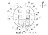
- FIG. 1 is an exploded perspective view showing an electronic device according to an embodiment of the present disclosure
- FIG. FIG. 2 is a perspective view showing the wiring board of FIG. 1
- FIG. 2 is a plan view of the front side of the wiring board of FIG. 1
- FIG. 2 is a plan view of the back side of the wiring board of FIG. 1
- FIG. 2 is a plan view of the back side of the wiring substrate of FIG. 1 excluding an insulating film
- It is the top view which expanded the circumference
- FIG. 2 is a side view showing the wiring substrate of FIG. 1
- FIG. 7 is a cross-sectional view taken along line AA of FIG. 6
- FIG. 7 is a cross-sectional view taken along line BB of FIG. 6
- FIG. 10 is a plan view showing another example of the wiring board according to the embodiment;
- FIG. 1 is an exploded perspective view showing an electronic device according to an embodiment of the present disclosure
- the electronic device 1 of the present embodiment includes an electronic component storage package 20 including a wiring board 10, a module board 30 on which the wiring board 10 is mounted, and components mounted on the wiring board 10. 50.
- the electronic component storage package 20 includes a wiring board 10 having a component mounting portion 101, a frame portion 21, and a lid 22.
- the frame portion 21 is joined to the wiring substrate 10 and the lid 22 to support the wiring substrate 10 and the lid 22 .
- the frame portion 21 may be made of metal and have a disc shape with a through hole 211 in the center.
- the frame portion 21 may be joined to the wiring board 10 on one surface around the opening of the through hole 211 .
- the component mounting portion 101 may be opened to the other through the through hole 211 .
- the lid 22 is joined to the other surface of the frame portion 21 and covers the component mounting portion 101 of the wiring board 10 .
- the lid 22 has an opening 221 through which light passes, and the opening 221 may be closed with a transparent member.
- the module substrate 30 may be FPC (Flexible printed circuits).
- the module board 30 has a plurality of electrodes 31 to 36 electrically connected to the wiring board 10 .
- the module substrate 30 has signal lines 37 to which high-frequency signals are input or output. A signal line 37 is connected to the electrode 35 .
- the component 50 includes an electronic component 51 and an optical component 52, and is mounted on the component mounting portion 101 of the wiring board 10.
- the component 50 may be mounted on the component mounting section 101 via the submount 55 .
- the electronic component 51 may be a component that inputs or outputs a high frequency signal.
- the electronic component 51 is an optical semiconductor component such as a semiconductor laser
- the optical component 52 is a prism that reflects the light emitted from the electronic component 51 toward the opening 221 of the lid 22 .
- the optical component 52 may be a lens
- the electronic component 51 may be a light receiving element such as a photodiode.
- the optical component 52 may be arranged according to the light emission position or the light incidence position.
- the electronic component 51 may be arranged according to the position of the optical component 52 .
- the component 50 may also include circuit components such as capacitors and resistive elements.
- FIG. 2 is a perspective view showing the wiring board of FIG.
- the perspective view is a view of the wiring substrate 10 viewed from the back side.
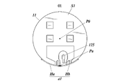
- 3 is a plan view of the front side of the wiring board of FIG. 1.
- FIG. 4A is a plan view of the back side of the wiring board of FIG. 1.
- FIG. 4B is a plan view of the back side of the wiring board with the insulating film removed.
- FIG. 5 is an enlarged plan view of the periphery of the ground electrode on the first surface.
- the wiring board 10 includes a base 11 having a first surface S1, a second surface S2 located on the opposite side of the first surface S1, and a side surface S3 extending from the first surface S1 to the second surface S2.
- the back side mentioned above is the side of the first surface S1 of the wiring board 10
- the front side mentioned above is the side of the second surface S2 of the wiring board 10.
- the base 11 may be formed by stacking dielectric materials.
- Dielectric materials include ceramic materials such as aluminum oxide sintered bodies, mullite sintered bodies, silicon carbide sintered bodies, aluminum nitride sintered bodies or silicon nitride sintered bodies, or glass ceramic materials. etc. can be used.
- the base 11 may have, for example, a circular shape when viewed from a direction (first direction) perpendicular to the first surface S1.
- the circular shape referred to here may include a shape in which a portion of the circle is cut off and a shape in which a portion of the circle protrudes.
- the size of the radius of the circle may be 0.5 mm to 5 mm
- the height of the substrate 11 may be 0.5 mm to 10 mm.
- the direction perpendicular to the first surface S1 is the height direction.
- At least one arc a1 is included in the outline of the base 11 when viewed from the direction perpendicular to the first surface S1.
- the outline may include a plurality of arcs a1 to a4 and a plurality of straight lines b1 to b4.
- the plurality of arcs a1 to a4 and the plurality of straight lines b1 to b4 may be arranged alternately.
- a plurality of arcs a1 to a4 may have the same center of curvature circle.
- the side surface S3 of the base 11 extends along the direction perpendicular to the first surface S1.
- the side surface S3 has a curved surface portion S3a and a flat surface portion S3b.
- Arcs a1 to a4 correspond to outlines when the curved surface portion S3a is viewed from a direction perpendicular to the first surface S1.
- the straight lines b1 to b4 correspond to outlines when the flat portion S3b is viewed from a direction perpendicular to the first surface S1.
- the second surface S2 side of the base 11 has a concave portion D1 that opens upward.
- the direction from the first surface S1 to the second surface S2 is defined as upward.
- the direction from the first surface S1 to the second surface S2 may be referred to as upward.
- the component mounting portion 101 may be positioned in the recess D1. That is, the submount 55 ( FIG. 1 ) may be mounted on the concave portion D ⁇ b>1 , and the component 50 described above may be mounted on the submount 55 .
- the wiring board 10 further includes electrodes (121 to 126) located on the first surface S1, electrodes (131 to 137) located on the second surface S2, and and inner conductors (141-146) located in the Further, the wiring substrate 10 includes an insulating film 15 covering part of the electrodes.
- the insulating film 15 may be an alumina coat.
- the electrodes positioned on the second surface S2 include a plurality of power supply electrodes 131-134, a signal electrode 135 through which high frequency signals are transmitted, and ground electrodes 136 and 137.
- the signal electrode 135 may be arranged at a position deviated from the center of the second surface S ⁇ b>2 according to the arrangement of the electronic component 51 .
- the optical component 52 may be centrally located on the second surface S2 and the electronic component 51 may be aligned with the optical component 52 and located off-center on the second surface S2. Due to the arrangement of the optical component 52, light can be emitted or incident from the central portion of the second surface S2. can be incident.
- the arrangement of the signal electrodes 135 as described above enables signal transmission with reduced power loss in accordance with the arrangement of the electronic components 51 .
- the signal electrode 135 may have a shape that is long on one side.
- the signal electrode 135 may be arranged such that its longitudinal direction is orthogonal to one side of the electronic component 51 . In this arrangement, even if the signal electrode 135 is extended in the longitudinal direction, the extended line does not overlap the center of the second surface S2.
- the ground electrode 136 surrounds the signal electrode 135 outside the recess D1.
- the ground electrode 137 is positioned on the inner bottom surface of the recess D1.
- the ground electrode 137 may also be positioned on a part of the inner side surface of the recess D1 and connected to the ground electrode 136 outside the recess D1.
- the power supply electrodes 131 to 134 may be positioned outside the recess D1 on the opposite side of the signal electrode 135 across the recess D1. That is, the power supply electrodes 131 to 134 may be positioned on one side of the recess D1, and the signal electrode 135 may be positioned on the other side of the recess D1.
- the electrodes positioned on the first surface S1 include a plurality of power supply electrodes 121 to 124, a signal electrode 125 through which high frequency signals are transmitted, and a ground electrode 126, as shown in FIGS. 4A and 4B.
- the ground electrode 126 surrounds the signal electrode 125 except for some areas. The partial range may be the vicinity of the outer edge of the first surface S ⁇ b>1 closest to the signal electrode 125 .
- the power electrodes 121 to 124 are located in a region opposite to the signal electrode 125 with the ground electrode 126 interposed therebetween. That is, the power electrodes 121 to 124 are positioned on one side of the ground electrode 126 and the signal electrode 125 is positioned on the other side of the ground electrode 126 .
- the power supply electrodes 121 to 124 may be arranged in two rows and two columns in the normal direction Y and the horizontal direction X (see FIG. 4A).
- the power supply electrodes 121-124 may be arranged symmetrically about the normal line L1 (FIG. 4A).
- the normal L1, the horizontal direction X, and the normal direction Y will be described later.
- the internal conductors located within the base 11 include power conductors 141 to 144 that electrically connect the power electrodes 121 to 124 on the first surface S1 and the power electrodes 131 to 134 on the second surface S2, respectively.
- each of the power supply conductors 141 to 144 includes a via conductor penetrating each dielectric layer and a film-like conductor positioned between two adjacent dielectric layers. It may be composed of a combination of conductors.
- the via conductor may have a cylindrical shape extending in a direction perpendicular to the first surface S1, and may be filled with a conductor.
- the internal conductors located within the base 11 further include signal conductors 145 that electrically connect the signal electrodes 125 on the first surface S1 and the signal electrodes 135 on the second surface S2.
- the signal conductor 145 may have a structure in which via conductors are connected in a straight line, or may have a structure in which a plurality of via conductors and one or a plurality of film conductors are connected in a stepwise manner.
- the film conductor of the signal conductor 145 may be strip-shaped.
- the internal conductors located within the base 11 further include a plurality of ground conductors 146 electrically connecting the ground electrode 126 on the first surface S1 and the ground electrodes 136, 137 on the second surface S2.
- Ground conductor 146 includes a plurality of via conductors connected in a straight line from first surface S1 to second surface S2.
- a plurality of ground conductors 146 are arranged around the signal conductor 145 at intervals that reduce leakage of high frequency signals. Any of a plurality of ground conductors 146 may be disposed between power conductors 141 - 144 and signal conductors 145 .
- the plurality of ground conductors 146 may include film conductors, and several ground conductors 146 may be electrically connected via one film conductor.
- the film-shaped conductor included in the ground conductor 146 may spread to the same extent as the ground electrodes 126, 136, and 137, may spread smaller than the ground electrodes 126, 136, and 137, or may be strip-shaped. good. In other words, when viewed through a plane in the height direction, the area of the film conductor included in the ground conductor 146 may be equal to or smaller than the areas of the ground electrodes 126, 136, and 137.
- the wiring board 10 further includes a first recess 16, a second recess 17, a first ground conductor 16A, a second ground conductor 17A, a first filling via (first via) 18 and a second filling via.
- a via (second via) 19 is provided.
- the first ground conductor 16 ⁇ /b>A is a film conductor and is positioned on the inner surface of the first recess 16 .
- the second ground conductor 17 ⁇ /b>A is a film conductor and is positioned on the inner surface of the second recess 17 .
- a portion of the first filling via 18 is exposed on the side surface S3.
- a part of the second filling via 19 is exposed on the side surface S3.
- a configuration having the first recess 16 and the first ground conductor 16A may be called a castellation.
- the configuration having the second recess 17 and the second ground conductor 17A may be called a castellation.
- the openings of the first recess 16 and the second recess 17 are positioned over the side surface S3 and the first surface S1.
- the first ground conductor 16A may be positioned at least on the first inner wall surface S16i (FIG. 7A) of the inner surface of the first recess 16 that is closer to the signal electrode 125. As shown in FIG.
- the first ground conductor 16A may be positioned on the entire inner surface of the first recess 16 .
- the second ground conductor 17A may be positioned at least on the second inner wall surface S17i (FIG. 7A) of the inner surface of the second recess 17 that is closer to the signal electrode 125 .
- the second ground conductor 17A may be positioned on the entire inner surface of the second recess 17 .
- the first ground conductor 16A and the second ground conductor 17A may be connected to the ground electrode 126 .
- the first filling via 18 is continuous with the first recess 16 at a position closer to the second surface S2 than the first recess 16 is.
- the second filling via 19 is continuous with the second recess 17 at a position closer to the second surface S ⁇ b>2 than the second recess 17 .
- the first filled via 18 and the second filled via 19 have a structure in which a hole in the base 11 is filled with a conductor, and a part of the conductor is exposed on the side surface S3.
- the first filled via 18 may be connected to the first ground conductor 16A.
- the second filled via 19 may be connected to the second ground conductor 17A.
- the signal line including the signal electrode 125, the signal conductor 145, and the signal electrode 135, and the surrounding configuration form a transmission line T1 for transmitting high-frequency signals.
- the surrounding configuration includes a dielectric (substrate 11) surrounding the signal line, and a plurality of ground conductors arranged around the signal line with the surrounding dielectric interposed therebetween.
- the ground conductors include the ground electrode 126 on the first surface S1, the ground conductor 146 in the base 11, the first ground conductor 16A, the second ground conductor 17A, the first filled via 18, the second filled via 19, and the second ground conductor.
- a ground electrode 136 on two sides S2 is included.
- the wiring board 10 can be manufactured by the following method as an example.
- the substrate 11 is composed of a ceramic material, a glass ceramic material, or the like
- a green sheet of the material before firing is provided with a conductive material and an insulating material to produce one sheet-like molding.
- the above-described conductive materials include the electrodes (121 to 126, 131 to 137), the first ground conductor 16A, the second ground conductor 17A, the first filled via 18, the second filled via 19 and the internal conductors (141 to 146).
- the insulating material mentioned above is a material for forming the insulating film 15 .
- the step of providing the conductive material and the insulating material may be performed layer by layer. That is, by forming a hole in the green sheet of each layer and filling the hole with a conductive paste, the via conductors of the internal conductors (141 to 146), the first filling via 18 and the second filling via are formed in the green sheet of each layer. Conductive material forming 19 may be provided. By pattern-printing a conductive paste on the surface of the green sheet of each layer, the green sheet of the intermediate layer can be provided with a conductive material for forming the film conductors of the internal conductors (141 to 146).
- a conductive material for forming electrodes (121 to 126, 131 to 137) can be provided on the surface green sheet. Furthermore, by forming holes in a green sheet of a predetermined layer and applying a conductive paste to the inner walls of the holes, the green sheet is provided with the first ground conductor 16A in the first recess 16 and the second recess 17. Conductive material may be provided forming the second ground conductor 17A within. After that, one sheet-like molding before firing is obtained by stacking a plurality of green sheets.
- the first concave portion 16 and the second concave portion 17 may be formed over one layer or a plurality of layers from the side closer to the first surface S1.
- the first ground conductor 16A and the second ground conductor 17A may be formed over one layer or a plurality of layers from the side closer to the first surface S1.
- the first filled via 18 and the second filled via 19 may be formed in a layer or layers located directly above the layer having the first recess 16 and the second recess 17 .
- the sheet-like molding is formed by forming one sheet-like molding in a state in which a plurality of moldings constituting individual wiring boards 10 are arranged vertically and horizontally so that a large number of wiring boards 10 can be obtained from one sheet-like molding. Made to be included in moldings.
- the sheet-shaped molded product is die-cut to form part of the outer shape of each individual molded product.
- adjacent molded products are processed into a form in which a part is connected so as not to separate a plurality of molded products.
- a curved surface portion S3a of the side surface S3 of the substrate 11 is formed in each molded product by the die-cutting process described above.
- the first recessed portion 16 and the second recessed portion 17 appear on the curved surface portion S3a of the side surface S3, and the first filling via 18 and the second filling via 19 are exposed on the curved surface portion S3a of the side surface S3.
- the curved surface portion S3a of the side surface S3 is a portion that includes arcs a1 to a4 when viewed from a direction perpendicular to the first surface S1.
- the sheet-shaped molding is fired.
- a fired product is obtained in which a plurality of molded products each serving as the wiring board 10 are arranged in a row.
- a plane portion S3b of the side surface S3 is formed by the cutting process.
- a plane portion S3b of the side surface S3 is a portion including straight lines b1 to b4 when viewed from a direction perpendicular to the first surface S1. Then, the separated individual molded products become one wiring board 10 .
- a large number of wiring boards 10 can be efficiently manufactured by the manufacturing method as described above.
- the electrodes 31 to 36 of the module substrate 30 are joined to the power supply electrodes 121 to 124, the signal electrode 125 and the ground electrode 126 of the wiring board 10 via a conductive joining material (brazing material or the like). However, a portion of the ground electrode 126 is covered with the insulating film 15 , and the portion of the ground electrode 126 not covered with the insulating film 15 is joined to the electrode 36 of the module substrate 30 .
- a conductive joining material (brazing material or the like).
- arc a1 located near signal electrode 125 has a symmetrical shape about normal L1 passing through the center point of arc a1.
- a normal to a circular arc means a straight line that is perpendicular to the tangent to the circular arc and contained on the same plane as the circular arc.
- the normal L1 may be a straight line included in the first surface S1 or a straight line parallel to the first surface S1.
- the normal L1 may overlap the center point of the first surface S1.
- a direction parallel to the first surface S1 and along the normal L1 is referred to as a normal direction Y.
- a direction parallel to the first surface S1 and perpendicular to the normal line L1 is referred to as a horizontal direction X.
- the width means the width in the horizontal direction X (dimension in the horizontal direction X), and left and right means one side and the other side in the horizontal direction X. As shown in FIG.
- the first recessed portion 16 and the second recessed portion 17 may overlap the arc a1 when viewed from the direction perpendicular to the first surface S1 and may be positioned with the signal electrode 125 interposed therebetween.
- the portion of the signal electrode 125 near the arc a1 can be sandwiched between the first ground conductor 16A in the first recess 16 and the second ground conductor 17A in the second recess 17 from left and right.
- a portion of the transmission line T1 (a portion near the first surface S1) can be sandwiched from the lateral direction X by the first ground conductor 16A and the second ground conductor 17A.
- the impedance of the transmission line T1 can be matched, and good high-frequency characteristics of signal transmission via the signal electrode 125 can be maintained.
- the bonding strength between the ground electrode 126 and the module substrate 30 can be improved. That is, when bonding the ground electrode 126 and the electrode 36 of the module substrate 30, part of the conductive bonding material flows into the first recess 16 and the second recess 17, and the first recess 16 and the second recess 17 and the module substrate 30, a fillet can be formed. The fillet improves the bonding strength, and can reduce damage to the bonding portion during use of the electronic device 1 .
- a ground electrode 126 may be positioned around the openings of the first recess 16 and the second recess 17 on the first surface S1. Additionally, the ground electrode 126 may be connected to the first ground conductor 16A and the second ground conductor 17A. Further, ground electrode 126 may be tangent to arc a1. The first concave portion 16 and the second concave portion 17 overlap the arc a1 when viewed from the direction perpendicular to the first surface S1, and the ground electrode 126 is in contact with the arc a1, thereby improving the bonding strength between the ground electrode 126 and the module substrate 30. can. That is, as shown in the previous description of the manufacturing method, the arc a1 portion is formed by die-cutting before firing.
- the conductive bonding material when the conductive bonding material is applied to the portion of the ground electrode 126 that overlaps the arc a1 after the die-cutting process, the conductive bonding material can hang down on the side surface S3. If the conductive bonding material hangs down on the side surface S3, when the ground electrode 126 is bonded to the electrode 36 of the module substrate 30, a fillet is likely to be formed between the side surface S3 and the electrode 36 of the module substrate 30. By forming the fillet, the bonding strength of the ground electrode 126 is improved, and damage to the bonding portion during use of the electronic device 1 can be reduced.
- the first concave portion 16 and the second concave portion 17 are arranged so as to overlap one arc a1 when viewed from the direction perpendicular to the first surface S1, so that the module substrate 30 and the wiring substrate 10 are separated from each other. It is possible to reduce the occurrence of damage such as cracks in the wiring board 10 at the time of bonding. That is, both ends of the arc a1 are likely to have a gentle angular shape such as a rounded shape when viewed from the direction perpendicular to the first surface S1.
- the arc a1 of this shape can be easily formed by die-cutting.
- first recess 16 and the second recess 17 are positioned with the signal electrode 125 interposed therebetween, they are close to the ends of the arc a1. Therefore, the ground electrode 126 located around the first concave portion 16 and the second concave portion 17 also tends to be close to the end of the arc a1. Therefore, thermal stress is likely to be applied to the end of the arc a1 when the ground electrode 126 and the electrode 36 of the module substrate 30 are joined together. Therefore, by forming the end portion of the arc a1 to which the stress is applied into a gentle angular shape, it is possible to reduce the occurrence of damage such as cracks in the portion.
- the signal electrode 125 may extend from the central region of the first surface S1 toward the arc a1 when viewed from the direction perpendicular to the first surface S1. With this configuration, it is possible to easily construct an arrangement in which the first concave portion 16 and the second concave portion 17 overlap the arc a1 and are positioned with the signal electrode 125 interposed therebetween.
- the signal electrode 125 When viewed in a direction perpendicular to the first surface S1, the signal electrode 125 extends from a first position pa (FIG. 4A) closer to the arc a1 than the center of the first surface S1 to a first electrode spaced apart from the outer edge of the first surface S1. It may extend as far as 2 positions pb (FIG. 4A).
- the first concave portion 16 and the second concave portion 17 can easily construct an arrangement in which the first concave portion 16 and the second concave portion 17 overlap the arc a1 and are positioned with the signal electrode 125 therebetween.
- the signal electrode 125 can be separated from By separating the signal electrode 125 from the edge of the first surface S1, it is possible to reduce the flow of the conductive bonding material to the side surface S3 of the base 11 when the signal electrode 125 is bonded to the electrode 34 of the module substrate 30. can. Therefore, it is possible to reduce the deterioration of the high-frequency characteristics of the transmission line T1 due to the generation of unnecessary capacitive components due to the conductive bonding material that has flowed to the side surface S3. In addition, short-circuiting of the signal electrode 125 to the ground electrode 126 via the conductive bonding material that has flowed to the side surface S3 can be reduced.
- the signal electrode 125 may have a shape in which the width changes stepwise from one end to the other end in the longitudinal direction.
- the signal electrode 125 may have a wider width at a portion far from the arc a1 than at a portion near the arc a1. With this shape, it is possible to match the impedance around the signal electrode 125 and maintain good high-frequency characteristics of signal transmission via the signal electrode 125 .
- the portion of the signal electrode 125 that has a wider width is located farther from the arc a1 than the first recess 16 and the second recess 17 are.
- the arrangement is suitable for impedance matching.
- the signal electrode 125 may be located deviated from the normal line L1. Since the signal electrodes 125 are positioned offset from the normal line L1, the signal lines of the transmission line T1 can be arranged in a linear manner corresponding to the offset arrangement of the signal electrodes 135 on the second surface S2. That is, when viewed from the longitudinal direction of the signal electrode 125, the signal electrode 125 on the first surface S1, the signal conductor 145 in the substrate 11, and the signal electrode 135 on the second surface S2 can be arranged in a straight line. can be done.
- the signal electrodes 125 on the first surface S1, the signal conductors 145 in the substrate 11, and the signal electrodes 135 on the second surface S2 are linearly arranged. can be brought closer to The signal line having this configuration can maintain good high-frequency characteristics of the transmission line T1.
- the arrangement deviating from the normal line L1 may mean an arrangement in which the signal electrodes 125 do not intersect the normal line L1.
- the biased arrangement may mean an arrangement in which, when the signal electrode 125 intersects the normal line L1, one area of the signal electrode 125 divided by the normal line L1 is different from the area of the other.
- the signal electrode 125 may have a shape that is long on one side when viewed in a direction perpendicular to the first surface S1.
- the longitudinal direction of the signal electrode 125 may be along the normal L1, or more specifically, parallel to the normal L1.
- the signal electrode 125 may face arc a 1 in the longitudinal direction of the signal electrode 125 .
- the first recess 16 and the second recess 17 may be arranged such that the distance from the first recess 16 to the signal electrode 125 and the distance from the second recess 17 to the signal electrode 125 match.
- the first concave portion 16 and the second concave portion 17 can be arranged symmetrically with respect to the signal electrode 125 which is located unevenly.
- the first concave portion 16 and the second concave portion 17 can be arranged symmetrically with respect to a plane passing through the longitudinal center line of the signal electrode 125 and perpendicular to the first surface S1.
- the signal electrode 125 and the signal conductor 145 in the substrate 11 may be arranged so as to overlap the plane from one end to the other end.
- the symmetrical arrangement described above can match the impedance of the transmission line T1 and maintain good high-frequency characteristics of the transmission line T1.
- the length Ln1 in the normal direction Y of the first recess 16 is the length Ln2 in the normal direction Y of the second recess 17 (dimension in the direction along the normal L1).
- FIG. 7A When the signal electrode 125, the first recess 16, and the second recess 17 are viewed through from the horizontal direction X such that they overlap, one end p16a of the first recess 16 and one end p16a of the second recess 17 The part p17a can be brought close to the same point. Alternatively, they can be superimposed on the same point. The one ends p16a and p17a are ends far from the arc a1.
- the one end portions of the first concave portion 16 and the second concave portion 17 can be arranged symmetrically with respect to the signal electrode 125 and the signal conductor 145 in the base 11 which are offset. Therefore, it is possible to match the impedance of the transmission line T1 and maintain good high frequency characteristics of the transmission line T1.
- the first recess 16 may be arranged closer to the normal line L1 than the signal electrode 125 when viewed from the direction perpendicular to the first surface S1. This arrangement can improve the overall bonding strength between the module substrate 30 and the base 11 . That is, on the first surface S1 of the base body 11 facing the module substrate 30, a portion where a large pressure can be generated by applying vibration or force to the base body 11 is the center of the outwardly protruding shaped portion. Therefore, when vibration or force is applied to the substrate 11, a large pressure is likely to be generated at the central point of the arc a1.
- the joint between the ground electrode 136 and the module substrate 30 can be arranged near the center point of the arc a1 where a large pressure is likely to occur. Since the bonding area between the ground electrode 126 and the module substrate 30 is large, high bonding strength can be obtained. Therefore, high bonding strength can be obtained at locations where large pressure is likely to occur, and overall bonding strength between the module substrate 30 and the base 11 is improved.
- the first recess 16 may be arranged so as to overlap the normal L1, but as shown in FIG. 4B, the first recess 16 may be arranged so as not to overlap the normal L1. According to this arrangement, since the ground electrode 126 can be joined to the module substrate 30 at the center point of the arc a1, the joining strength between the wiring substrate 10 and the module substrate 30 can be further improved.
- the ground electrode 126 has a larger area than the signal electrode 125, and may surround the signal electrode 125 except for a part of the area on the arc a1 side from the signal electrode 125. With this configuration of the ground electrode 126 , it is possible to match the impedance around the signal electrode 125 and maintain good high-frequency characteristics of signal transmission through the signal electrode 125 .
- the ground electrode 126 has a first region F1 closer to the first recess 16 than the second recess 17 and a second region F2 closer to the second recess 17 than the first recess 16. .
- the first area F1 may be larger than the second area F2.
- the left side of the boundary line E1 is the first area F1
- the right side of the boundary line E1 is the second area F2.
- the first area F1 and the second area F2 may be defined as one and the other when the ground electrode 126 is divided by the center line of the signal electrode 125 (the center line extending in the longitudinal direction).
- the first recess 16 located in the first region F1 has a longer length in the normal direction Y than the second recess 17 located in the second region F2, and is located closer to the normal L1. be. Since the ground electrode 126 has the first region F1, many ground conductors 146 (via conductors) can be connected to the large-area first region F1. Propagation of noise can be reduced. This is because the power supply electrodes 121 to 124 may be arranged symmetrically with respect to the normal L1, in which case the power supply electrodes 121, 122 located on the opposite side of the normal L1 to the signal electrode 125 are the signal electrodes 121-124. The electrodes 125 are widely spaced laterally.
- the noise when noise occurs, the noise propagates in a direction oblique to the normal line L1 between the power supply electrodes 121 and 122 and the transmission line T1, which are widely separated in the horizontal direction. Therefore, the propagation of the noise can be reduced by the first area F1 of the ground electrode 126 having a large area and many ground conductors 146 (via conductors) connected to the first area F1.
- the width of the portion of the ground electrode 126 contacting the arc a1 may be the same in the first region F1 and the second region F2. That is, the ground electrodes 126 located on both left and right sides of the first recess 16 may have the same width as the ground electrodes 126 located on both left and right sides of the second recess 17 in the arc a1.
- the impedance of the transmission line T1 can be appropriately matched by the ground electrode, and good high-frequency characteristics of the transmission line T1 can be maintained.
- the horizontal width of the edge 126e (FIG. 4B) of the ground electrode 126 on the far side from the arc a1 is substantially the same as the width from the left end position p1 to the right end position p2 of the region in which the power supply electrodes 121 to 124 are arranged. Alternatively, it may be larger than the horizontal width. This configuration can further reduce noise propagation between the power supply electrodes 121 to 124 and the transmission line T1.
- the large-area ground electrode 126 may be partially covered with the insulating film 15 (FIG. 4A). At that time, the first region F1 having a large area may be covered with the insulating film 15 in a larger range than the second region F2 having a small area.
- the insulating film 15 By being covered with the insulating film 15, when the ground electrode 126 and the electrode 36 of the module substrate 30 are bonded together, uneven thickness of the conductive bonding material can be reduced. can improve the bonding strength of
- the side closer to the second surface S2 than the first recess 16 and the second recess 17 has the first filling via 18 and the second filling via 19, and the first filling via 18 may be connected to the first ground conductor 16A and the second filled via 19 may be connected to the second ground conductor 17A.
- the first filled via 18 and the second filled via 19 are via conductors whose internal conductors are exposed to the side surface S ⁇ b>3 of the base 11 .
- the first filling via 18 and the second filling via 19 can sandwich the portion of the transmission line T1 near the side surface S3 from the lateral direction X, and the impedance of the transmission line T1 can be reduced to can be aligned. Therefore, good high-frequency characteristics of the transmission line T1 can be maintained.
- the first filling via 18 and the second filling via 19 compared to the case where the first recess 16 and the second recess 17 are formed long to the locations of the first filling via 18 and the second filling via 19, , which has the advantage of reducing manufacturing costs.
- the first filled via 18 and the second filled via 19 can be formed by the same process as the via conductors of the internal conductors (141 to 146).
- the first recess 16 having the film-like first ground conductor 16A inside and the second recess 17 having the film-like second ground conductor 17A inside are shaped like via conductors in the green sheet.
- the conductive paste is applied only to the inner periphery of the hole, a process separate from that for the via conductor is required. Therefore, by adopting the first filled via 18 and the second filled via 19, the number of layers of the green sheets requiring the separate process can be reduced, and the manufacturing cost can be reduced.
- FIG. 6 is a side view showing the wiring board 10 of FIG. 7A and 7B show a cross section of a part of the wiring board 10.
- FIG. 7A is a cross sectional view taken along line AA of FIG. 6, and
- FIG. 7B is a cross sectional view taken along line BB of FIG.
- FIG. 6 corresponds to a side view of the wiring board 10 viewed from the normal direction Y.
- FIG. 7A is a cross sectional view taken along line AA of FIG. 6
- FIG. 7B is a cross sectional view taken along line BB of FIG.
- FIG. 6 corresponds to a side view of the wiring board 10 viewed from the normal direction Y.
- the first concave portion 16 and the second concave portion 17 may have a shape in which the dimension in the normal direction Y is longer than the dimension in the lateral direction X in the cross section parallel to the first surface S1.
- the first filling via 18 and the second filling via 19 have a shape in which the dimension in the normal direction Y is longer than the dimension in the lateral direction X in the cross section parallel to the first surface S1.
- the longitudinal direction of the first recess 16, the second recess 17, the first filling via 18, and the second filling via 19 may be parallel to the longitudinal direction of the signal electrode 125 or parallel to the normal direction Y. good too.
- first ground conductor 16A may be positioned at least on the first inner wall surface S16i (FIG. 7A) of the inner surface of the first recess 16 that is closer to the signal electrode 125.
- second ground conductor 17A may be positioned at least on the second inner wall surface S17i (FIG. 7A) of the inner surface of the second recess 17 that is closer to the signal electrode 125. As shown in FIG.
- the side closer to the side surface S3 of the transmission line T1 is positioned by the wider surface of the ground conductor. It can be sandwiched from the lateral direction X.
- the side of the transmission line T1 closer to the side surface S3 can be sandwiched in the horizontal direction X by the wide surface of the ground conductor. Therefore, the ground conductor can match the impedance of the transmission line T1 and maintain good high-frequency characteristics of the transmission line T1.
- the first concave portion 16 and the second concave portion 17 have rounded inner corners (farther from the arc a1) (corresponding to the shape of the corners near the signal electrode 125). good too. That is, the first recessed portion 16 and the second recessed portion 17 may have a cross-sectional shape obtained by cutting an elliptical or elongated hole shape (an elongated hole shape having semicircular ends at one end and the other end) in the longitudinal direction. Stress relaxation can be achieved by having the said roundness of the 1st recessed part 16 and the 2nd recessed part 17. FIG. Therefore, the bonding strength when bonding the electrode 35 of the module substrate 30 and the ground electrode 126 of the wiring substrate 10 can be improved.
- the first filling via 18 and the second filling via 19 have rounded inner corners (farther from the arc a1) (corresponding to the shape of the corners near the signal electrode 125).
- the first filling via 18 and the second filling via 19 may have a cross-sectional shape obtained by cutting an elliptical or elongated hole shape (one end and the other end of which are semicircular elongated holes) in the longitudinal direction. good. This shape facilitates the process of filling conductive paste into the holes to be the first filled via 18 and the second filled via 19 when fabricating the first filled via 18 and the second filled via 19 .
- the first filled via 18 and the second filled via 19 may be separated from the second surface S2 as shown in FIG. With this configuration, the volumes of the first filled via 18 and the second filled via 19 can be reduced. Therefore, the stress generated at the interface between the first filled via 18 and the second filled via 19 cooled after the sintering process in the manufacturing process and the substrate 11 can be reduced. Furthermore, since the conductor lumps, which are the first filled vias 18 and the second filled vias 19, are located in the base 11 on the side closer to the second surface S2, peeling of the first filled vias 18 and the second filled vias 19, etc. damage can be reduced.
- the width (horizontal dimension) w1 of the first recess 16 may be larger than the width (horizontal dimension) w2 of the first filling via 18 .
- the lateral width (horizontal dimension) w3 of the second recess 17 may be larger than the lateral width (horizontal dimension) w4 of the second filling via 19 . Since the widths w1 and w3 of the first recess 16 and the second recess 17 are large, when the electrode 35 of the module substrate 30 and the ground electrode 126 of the wiring board 10 are joined, the conductive bonding material is It easily flows into the second concave portion 17 . And the joining strength of the said joining part can be improved by the said inflow.
- the volume of the first filled via 18 and the second filled via 19 can be reduced.
- the small volume can reduce the stress generated at the interface between the first filled via 18 and the second filled via 19 cooled after the sintering process in the manufacturing process and the substrate 11 .
- damage such as peeling of the first filling via 18 and the second filling via 19 can be reduced. Therefore, by satisfying the above magnitude relationship for the widths of the first recessed portion 16 and the second recessed portion 17 and the first filled via 18 and the second filled via 19, it is possible to improve both the bonding strength and the reduction of via peeling. can be planned.
- the first recess 16 and the first filling via 18 having different widths w1 and w2 may be arranged so that the side surfaces close to the signal electrode 125 overlap at the same position when seen through from the direction perpendicular to the first surface S1.
- the second recess 17 and the second filling via 19 having different lateral widths w3 and w4 are arranged so that the side surfaces close to the signal electrode 125 overlap at the same position when seen through from the direction perpendicular to the first surface S1.
- the width w1 of the first recess 16 and the width w3 of the second recess 17 may be constant along the height direction, or may vary along the height direction. good too. Manufacturing is easy when the width w1 of the first recess 16 and the width w3 of the second recess 17 are constant along the height direction. Also, the width w2 of the first filling via 18 and the width w4 of the second filling via 19 may be constant along the height direction as shown in FIG. 6, or may be constant along the height direction. may have changed. When each of the width w2 of the first filling via 18 and the width w4 of the second filling via 19 is constant along the height direction, the number of man-hours in the manufacturing process when the substrate 11 has a laminated structure can be reduced.
- the width w1 of the first recess 16 and/or the width w2 of the first filling via 18 change along the height direction
- the width w1 of the first recess 16 is greater than the width w2 of the first filling via 18. Also larger may mean that the minimum value of the lateral width w1 of the first recess 16 is greater than the maximum value of the lateral width w2 of the first filling via 18 .
- the wiring board 10 and the electronic component storage package 20 of the present embodiment while maintaining good high-frequency characteristics, damage to the components when mounted on the module board 30 is reduced. An advantage is obtained that the bonding strength with 30 can be improved. Further, according to the electronic device 1 of the present embodiment, by having the electronic component storage package 20, it is possible to improve the reliability of the bonding between the module substrate 30 and the wiring substrate 10 while maintaining good high frequency characteristics. You get the advantage.
- the outer shape of the substrate 11 when viewed from the direction perpendicular to the first surface S1 has a plurality of arcs a1 to a4 and a plurality of straight lines b1 to b4.
- the base 11 may have, for example, a circular outer shape when viewed from the direction perpendicular to the first surface S1.
- FIG. 8 is a plan view showing another example of the wiring board 10 according to the embodiment.
- the arc a1 included in the outer shape may be defined based on the signal electrode 125 positioned on the first surface S1.
- a straight line O1 that is parallel to the longitudinal direction of the signal electrode 125 and passes through the center P0 of the circle is set on a plane viewed from a direction perpendicular to the first surface S1.
- the intersection on the side closer to the signal electrode 125 is defined as a reference point Pa.
- a single arc a1 may be defined as a combination of ranges Ha and Hb that are equidistant from the reference point Pa in the clockwise direction and the counterclockwise direction along the circle.
- the first filling via 18 is provided above the first recess 16 and the second filling via 19 is provided above the second recess 17. At least one of the filling vias 19 may not be provided. For example, at least one of the first recess 16 and the second recess 17 may extend to the vicinity of the second surface S2 in the height direction without providing a filling via.
- the wiring substrate 10 has the film-like power electrodes 121 to 124, the signal electrode 125 and the ground electrode 126, and the power electrodes 121 to 124, the signal electrode 125 and the ground electrode 126 are the module substrate 30.
- a configuration in which the electrodes 31 to 36 are respectively joined is shown.
- the wiring board 10 may have a plurality of electrode pins instead of the film-shaped power electrodes 121 to 124 , the signal electrode 125 and the ground electrode 126 , and the plurality of electrode pins may be connected to the module substrate 30 .
- the electronic component storage package may have a TO (Transistor Outline)-Can type configuration.
- the number and arrangement of various electrodes and electrode pins can be appropriately selected according to the components to be mounted.
- the details shown in the embodiment can be changed as appropriate without departing from the gist of the present disclosure.
- the present invention can be used for wiring boards, electronic component storage packages, and electronic devices.
Landscapes
- Engineering & Computer Science (AREA)
- Microelectronics & Electronic Packaging (AREA)
- Physics & Mathematics (AREA)
- Condensed Matter Physics & Semiconductors (AREA)
- General Physics & Mathematics (AREA)
- Electromagnetism (AREA)
- Optics & Photonics (AREA)
- Structure Of Printed Boards (AREA)
- Shielding Devices Or Components To Electric Or Magnetic Fields (AREA)
Priority Applications (3)
| Application Number | Priority Date | Filing Date | Title |
|---|---|---|---|
| US18/572,653 US20240292530A1 (en) | 2021-06-21 | 2022-06-17 | Wiring board, electronic component storage package, and electronic device |
| CN202280043595.1A CN117546613A (zh) | 2021-06-21 | 2022-06-17 | 布线基板、电子部件收纳用封装件以及电子装置 |
| JP2023530429A JP7660676B2 (ja) | 2021-06-21 | 2022-06-17 | 配線基板、電子部品収納用パッケージ及び電子装置 |
Applications Claiming Priority (2)
| Application Number | Priority Date | Filing Date | Title |
|---|---|---|---|
| JP2021102349 | 2021-06-21 | ||
| JP2021-102349 | 2021-06-21 |
Publications (1)
| Publication Number | Publication Date |
|---|---|
| WO2022270429A1 true WO2022270429A1 (ja) | 2022-12-29 |
Family
ID=84545692
Family Applications (1)
| Application Number | Title | Priority Date | Filing Date |
|---|---|---|---|
| PCT/JP2022/024287 Ceased WO2022270429A1 (ja) | 2021-06-21 | 2022-06-17 | 配線基板、電子部品収納用パッケージ及び電子装置 |
Country Status (5)
| Country | Link |
|---|---|
| US (1) | US20240292530A1 (https=) |
| JP (1) | JP7660676B2 (https=) |
| CN (1) | CN117546613A (https=) |
| TW (1) | TW202310686A (https=) |
| WO (1) | WO2022270429A1 (https=) |
Citations (4)
| Publication number | Priority date | Publication date | Assignee | Title |
|---|---|---|---|---|
| JPH11312760A (ja) * | 1998-04-28 | 1999-11-09 | Kyocera Corp | 高周波用配線基板 |
| JP2012238640A (ja) * | 2011-05-10 | 2012-12-06 | Shinko Electric Ind Co Ltd | 光半導体素子用パッケージ及び光半導体装置 |
| JP2014197086A (ja) * | 2013-03-29 | 2014-10-16 | コニカミノルタ株式会社 | 光通信用モジュール又は光通信ユニット |
| WO2020138209A1 (ja) * | 2018-12-26 | 2020-07-02 | 京セラ株式会社 | 配線基体、電子部品収納用パッケージおよび電子装置 |
-
2022
- 2022-06-17 JP JP2023530429A patent/JP7660676B2/ja active Active
- 2022-06-17 US US18/572,653 patent/US20240292530A1/en active Pending
- 2022-06-17 CN CN202280043595.1A patent/CN117546613A/zh active Pending
- 2022-06-17 WO PCT/JP2022/024287 patent/WO2022270429A1/ja not_active Ceased
- 2022-06-21 TW TW111122971A patent/TW202310686A/zh unknown
Patent Citations (4)
| Publication number | Priority date | Publication date | Assignee | Title |
|---|---|---|---|---|
| JPH11312760A (ja) * | 1998-04-28 | 1999-11-09 | Kyocera Corp | 高周波用配線基板 |
| JP2012238640A (ja) * | 2011-05-10 | 2012-12-06 | Shinko Electric Ind Co Ltd | 光半導体素子用パッケージ及び光半導体装置 |
| JP2014197086A (ja) * | 2013-03-29 | 2014-10-16 | コニカミノルタ株式会社 | 光通信用モジュール又は光通信ユニット |
| WO2020138209A1 (ja) * | 2018-12-26 | 2020-07-02 | 京セラ株式会社 | 配線基体、電子部品収納用パッケージおよび電子装置 |
Also Published As
| Publication number | Publication date |
|---|---|
| JP7660676B2 (ja) | 2025-04-11 |
| US20240292530A1 (en) | 2024-08-29 |
| CN117546613A (zh) | 2024-02-09 |
| JPWO2022270429A1 (https=) | 2022-12-29 |
| TW202310686A (zh) | 2023-03-01 |
Similar Documents
| Publication | Publication Date | Title |
|---|---|---|
| US11751480B2 (en) | Electronic device | |
| CN109937533B (zh) | 晶体振动器件 | |
| US10848125B2 (en) | Quartz crystal resonator unit | |
| US10425057B2 (en) | Quartz crystal blank and quartz crystal resonator unit | |
| US10135420B2 (en) | Quartz crystal blank and quartz crystal resonator unit | |
| CN109804562B (zh) | 压电振动器件 | |
| CN107534427A (zh) | 压电振动器件 | |
| WO2017110308A1 (ja) | 弾性波装置 | |
| US10411673B2 (en) | Quartz crystal blank and quartz crystal resonator unit | |
| US9985604B2 (en) | Quartz crystal blank and quartz crystal resonator unit | |
| US10027309B2 (en) | Quartz crystal blank and quartz crystal resonator unit | |
| JP7683725B2 (ja) | サーミスタ搭載型圧電振動デバイス | |
| US10418964B2 (en) | Quartz crystal blank and quartz crystal resonator unit | |
| CN107211221B (zh) | 压电元件以及具备该压电元件的超声波传感器 | |
| WO2022270429A1 (ja) | 配線基板、電子部品収納用パッケージ及び電子装置 | |
| CN114762098B (zh) | 电子部件收纳用封装件、电子装置及电子模块 | |
| US6806626B2 (en) | Electronic component | |
| JP5735822B2 (ja) | 圧電発振器 | |
| US10361675B2 (en) | Quartz crystal blank and quartz crystal resonator unit | |
| JP7018968B2 (ja) | 配線基板、電子装置及び電子モジュール | |
| US9985603B2 (en) | Quartz crystal blank and quartz crystal resonator unit | |
| JP2022183454A (ja) | 弾性波デバイス | |
| WO2020262472A1 (ja) | 電子部品収納用パッケージ、電子装置、および電子モジュール | |
| JP2024157184A (ja) | 弾性波デバイス | |
| JP2022086505A (ja) | 圧電共振デバイス |
Legal Events
| Date | Code | Title | Description |
|---|---|---|---|
| 121 | Ep: the epo has been informed by wipo that ep was designated in this application |
Ref document number: 22828346 Country of ref document: EP Kind code of ref document: A1 |
|
| WWE | Wipo information: entry into national phase |
Ref document number: 202280043595.1 Country of ref document: CN |
|
| WWE | Wipo information: entry into national phase |
Ref document number: 18572653 Country of ref document: US Ref document number: 2023530429 Country of ref document: JP |
|
| NENP | Non-entry into the national phase |
Ref country code: DE |
|
| 122 | Ep: pct application non-entry in european phase |
Ref document number: 22828346 Country of ref document: EP Kind code of ref document: A1 |