WO2022255341A1 - 駆動装置及び超音波センサ - Google Patents
駆動装置及び超音波センサ Download PDFInfo
- Publication number
- WO2022255341A1 WO2022255341A1 PCT/JP2022/022068 JP2022022068W WO2022255341A1 WO 2022255341 A1 WO2022255341 A1 WO 2022255341A1 JP 2022022068 W JP2022022068 W JP 2022022068W WO 2022255341 A1 WO2022255341 A1 WO 2022255341A1
- Authority
- WO
- WIPO (PCT)
- Prior art keywords
- power supply
- drive
- supply circuit
- circuit
- ultrasonic sensor
- Prior art date
- Legal status (The legal status is an assumption and is not a legal conclusion. Google has not performed a legal analysis and makes no representation as to the accuracy of the status listed.)
- Ceased
Links
Images




Classifications
-
- G—PHYSICS
- G01—MEASURING; TESTING
- G01S—RADIO DIRECTION-FINDING; RADIO NAVIGATION; DETERMINING DISTANCE OR VELOCITY BY USE OF RADIO WAVES; LOCATING OR PRESENCE-DETECTING BY USE OF THE REFLECTION OR RERADIATION OF RADIO WAVES; ANALOGOUS ARRANGEMENTS USING OTHER WAVES
- G01S7/00—Details of systems according to groups G01S13/00, G01S15/00, G01S17/00
- G01S7/52—Details of systems according to groups G01S13/00, G01S15/00, G01S17/00 of systems according to group G01S15/00
- G01S7/523—Details of pulse systems
- G01S7/524—Transmitters
-
- G—PHYSICS
- G01—MEASURING; TESTING
- G01S—RADIO DIRECTION-FINDING; RADIO NAVIGATION; DETERMINING DISTANCE OR VELOCITY BY USE OF RADIO WAVES; LOCATING OR PRESENCE-DETECTING BY USE OF THE REFLECTION OR RERADIATION OF RADIO WAVES; ANALOGOUS ARRANGEMENTS USING OTHER WAVES
- G01S15/00—Systems using the reflection or reradiation of acoustic waves, e.g. sonar systems
- G01S15/02—Systems using the reflection or reradiation of acoustic waves, e.g. sonar systems using reflection of acoustic waves
- G01S15/06—Systems determining the position data of a target
- G01S15/08—Systems for measuring distance only
- G01S15/10—Systems for measuring distance only using transmission of interrupted, pulse-modulated waves
-
- H—ELECTRICITY
- H02—GENERATION; CONVERSION OR DISTRIBUTION OF ELECTRIC POWER
- H02M—APPARATUS FOR CONVERSION BETWEEN AC AND AC, BETWEEN AC AND DC, OR BETWEEN DC AND DC, AND FOR USE WITH MAINS OR SIMILAR POWER SUPPLY SYSTEMS; CONVERSION OF DC OR AC INPUT POWER INTO SURGE OUTPUT POWER; CONTROL OR REGULATION THEREOF
- H02M1/00—Details of apparatus for conversion
- H02M1/36—Means for starting or stopping converters
-
- H—ELECTRICITY
- H02—GENERATION; CONVERSION OR DISTRIBUTION OF ELECTRIC POWER
- H02M—APPARATUS FOR CONVERSION BETWEEN AC AND AC, BETWEEN AC AND DC, OR BETWEEN DC AND DC, AND FOR USE WITH MAINS OR SIMILAR POWER SUPPLY SYSTEMS; CONVERSION OF DC OR AC INPUT POWER INTO SURGE OUTPUT POWER; CONTROL OR REGULATION THEREOF
- H02M3/00—Conversion of DC power input into DC power output
- H02M3/02—Conversion of DC power input into DC power output without intermediate conversion into AC
- H02M3/04—Conversion of DC power input into DC power output without intermediate conversion into AC by static converters
- H02M3/06—Conversion of DC power input into DC power output without intermediate conversion into AC by static converters using resistors or capacitors, e.g. potential divider
- H02M3/07—Conversion of DC power input into DC power output without intermediate conversion into AC by static converters using resistors or capacitors, e.g. potential divider using capacitors charged and discharged alternately by semiconductor devices with control electrode, e.g. charge pumps
-
- G—PHYSICS
- G01—MEASURING; TESTING
- G01S—RADIO DIRECTION-FINDING; RADIO NAVIGATION; DETERMINING DISTANCE OR VELOCITY BY USE OF RADIO WAVES; LOCATING OR PRESENCE-DETECTING BY USE OF THE REFLECTION OR RERADIATION OF RADIO WAVES; ANALOGOUS ARRANGEMENTS USING OTHER WAVES
- G01S15/00—Systems using the reflection or reradiation of acoustic waves, e.g. sonar systems
- G01S15/02—Systems using the reflection or reradiation of acoustic waves, e.g. sonar systems using reflection of acoustic waves
- G01S15/50—Systems of measurement, based on relative movement of the target
- G01S15/58—Velocity or trajectory determination systems; Sense-of-movement determination systems
-
- G—PHYSICS
- G01—MEASURING; TESTING
- G01S—RADIO DIRECTION-FINDING; RADIO NAVIGATION; DETERMINING DISTANCE OR VELOCITY BY USE OF RADIO WAVES; LOCATING OR PRESENCE-DETECTING BY USE OF THE REFLECTION OR RERADIATION OF RADIO WAVES; ANALOGOUS ARRANGEMENTS USING OTHER WAVES
- G01S15/00—Systems using the reflection or reradiation of acoustic waves, e.g. sonar systems
- G01S15/88—Sonar systems specially adapted for specific applications
-
- G—PHYSICS
- G01—MEASURING; TESTING
- G01S—RADIO DIRECTION-FINDING; RADIO NAVIGATION; DETERMINING DISTANCE OR VELOCITY BY USE OF RADIO WAVES; LOCATING OR PRESENCE-DETECTING BY USE OF THE REFLECTION OR RERADIATION OF RADIO WAVES; ANALOGOUS ARRANGEMENTS USING OTHER WAVES
- G01S15/00—Systems using the reflection or reradiation of acoustic waves, e.g. sonar systems
- G01S15/88—Sonar systems specially adapted for specific applications
- G01S15/93—Sonar systems specially adapted for specific applications for anti-collision purposes
- G01S15/931—Sonar systems specially adapted for specific applications for anti-collision purposes of land vehicles
Definitions
- the invention disclosed in this specification relates to a driving device for driving a driven element and an ultrasonic sensor including the driving device.
- the ultrasonic sensor disclosed in Patent Literature 1 includes a driving circuit that drives a piezoelectric element (transmitting section that transmits an output signal in the ultrasonic range using the piezoelectric element).
- the drive circuit operates using the voltage supplied from the power supply circuit as the power supply voltage.
- the driving circuit pulse-drives the driven element
- the switching noise of the power supply circuit may adversely affect the signal processing of the driven element.
- the drive device disclosed in this specification includes a power supply circuit including a switch element, and a drive circuit configured to pulse-drive an element to be driven using a voltage supplied from the power supply circuit as a power supply voltage. , provided.
- the power supply circuit is configured to operate such that the switching frequency of the switch element and the frequency of the pulse drive are different.
- the ultrasonic sensor disclosed in this specification includes a piezoelectric element and the driving device configured as described above and configured to drive the piezoelectric element.
- the driving device and the ultrasonic sensor disclosed in this specification it is possible to prevent the switching noise of the power supply circuit from adversely affecting the signal processing of the element to be driven.
- FIG. 1 is a diagram showing a schematic configuration of an ultrasonic sensor according to a first comparative example.
- FIG. 2 is a diagram showing waveforms of voltages of the ultrasonic sensor according to the first comparative example.
- FIG. 3 is a diagram showing a schematic configuration of an ultrasonic sensor according to a second comparative example.
- FIG. 4 is a diagram showing a schematic configuration of an ultrasonic sensor according to the first embodiment.
- FIG. 5 is a diagram showing waveforms of voltages of the ultrasonic sensor according to the first embodiment.
- FIG. 6 is a diagram showing a schematic configuration of an ultrasonic sensor according to the second embodiment.
- FIG. 7 is a diagram showing waveforms of voltages of the ultrasonic sensor according to the second embodiment.
- FIG. 1 is a diagram showing a schematic configuration of an ultrasonic sensor according to a first comparative example.
- FIG. 2 is a diagram showing waveforms of voltages of the ultrasonic sensor according to the first comparative example.
- FIG. 8 is a diagram showing an example of frequencies of switching noise in a power supply circuit.
- FIG. 9 is a diagram showing an example of the signal strength of the drive signal and the signal strength of the switching noise of the power supply circuit.
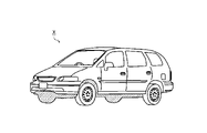
- FIG. 10 is an external view of the vehicle.
- FIG. 11 is a diagram showing waveforms of voltages in the second mode of the ultrasonic sensor according to the modification of the first embodiment.
- a constant voltage means a voltage that is constant in an ideal state, and is actually a voltage that can slightly fluctuate due to temperature changes and the like.
- the reference voltage means a voltage that is constant in an ideal state, and is actually a voltage that can slightly fluctuate due to temperature changes and the like.
- FIG. 1 is a diagram showing a schematic configuration of an ultrasonic sensor according to a first comparative example.
- the ultrasonic sensor 11 shown in FIG. 1 includes a control circuit 1, a clock signal generator 2, a power supply circuit 3, a drive circuit A2, a piezoelectric element PZ1, and a receiver circuit A3.
- the ultrasonic sensor 11 senses the distance to the object to be measured.
- the clock signal generator 2 generates a clock signal with a predetermined frequency.
- the power supply circuit 3 generates the output voltage VOUT by switching the switch element based on the clock signal output from the clock signal generator 2 .
- the power supply circuit 3 is a charge pump circuit that includes an amplifier A1 that amplifies a clock signal, a diode D1 that is a switching element, a flying capacitor C1, a diode D2, and a capacitor C2.
- a clock signal is supplied to the input of amplifier A1.
- the output terminal of amplifier A1 is connected to the negative terminal of flying capacitor C1.
- a first constant voltage VCC1 is applied to the anode of the diode D1 and the power supply terminal of the amplifier A1.
- the ground end of amplifier A1 is connected to ground potential.
- the cathode of the diode D1 is connected to the positive terminal of the flying capacitor C1 and the anode of the diode D2.
- the cathode of diode D2 is connected to the positive terminal of capacitor C2.
- the negative terminal of capacitor C2 is connected to ground potential.
- the positive electrode voltage of the capacitor C2 becomes the output voltage VOUT of the power supply circuit 3 .
- the drive circuit A2 uses the voltage supplied from the power supply circuit 3 as a power supply voltage, and is configured to pulse-drive the piezoelectric element PZ1.
- the drive circuit A2 is an amplifier that amplifies the control signal output from the control circuit 1 .
- the control circuit 1 outputs a plurality of pulse signals as control signals during the transmission operation of the ultrasonic sensor 11, and outputs a fixed LOW level signal as the control signal during the reception operation of the ultrasonic sensor 11.
- the drive circuit A2 vibrates the piezoelectric element PZ1 in the ultrasonic range.
- a control signal output from the control circuit 1 is supplied to the input end of the drive circuit A2.
- the output end of the driving circuit A2 is connected to the first end of the piezoelectric element PZ1 and the input end of the receiving circuit A3.
- the output voltage VOUT of the power supply circuit 3 is applied to the power supply end of the drive circuit A2.
- the ground end of the driving circuit A2 and the second end of the piezoelectric element PZ1 are connected to the ground potential.
- the receiving circuit A3 uses the second constant voltage VCC2 as a power supply voltage and receives the output signal of the piezoelectric element PZ1.
- the receiving circuit A3 is an amplifier that amplifies the output signal of the piezoelectric element PZ1.
- the output signal of the piezoelectric element PZ1 is supplied to the input terminal of the receiving circuit A3.
- the output signal of the receiving circuit A3 is supplied to the control circuit 1.
- FIG. A second constant voltage VCC2 is applied to the power terminal of the receiving circuit A3.
- the ground end of the receiving circuit A3 is connected to the ground potential.
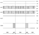
- FIG. 2 is a diagram showing waveforms of voltages of the ultrasonic sensor 11.
- FIG. 2 shows the first constant voltage VCC1, the positive voltage VCP of the flying capacitor C1, the negative voltage VCN of the flying capacitor C1, the output voltage VOUT of the power supply circuit 3, and the drive voltage VDRV output from the drive circuit A2.
- VCC1 the first constant voltage
- VCP the positive voltage
- VCN the negative voltage
- VOUT the output voltage
- VDRV output from the drive circuit A2 is a diagram showing each waveform of . Note that 35 V and 70 V in FIG. 2 are merely examples, and other values may be used.
- the diode D1 When the clock signal is at LOW level, the diode D1 is turned on to charge the flying capacitor C1, and when the positive voltage VCP of the flying capacitor C1 reaches 35V, the diode D1 is turned off. Then, when the clock signal switches from the LOW level to the HIGH level, the diode D1 remains off, the negative electrode voltage VCN of the flying capacitor C1 rises to 35V, the positive electrode voltage VCP of the flying capacitor C1 rises to 70V, and the flying capacitor C1 rises to 70V. Capacitor C1 discharges.
- the ultrasonic sensor 11 has a problem that the output voltage of the power supply circuit 3 cannot be controlled to an arbitrary value because the output voltage of the power supply circuit 3 depends on the first constant voltage VCC1.
- the ultrasonic sensor according to the second comparative example is an ultrasonic sensor that can solve the problem.
- FIG. 3 is a diagram showing a schematic configuration of an ultrasonic sensor according to a second comparative example.
- the ultrasonic sensor 12 shown in FIG. 3 has a configuration in which resistors R1 and R2, a comparator COMP1, a reference voltage source REF1, and an AND gate AND1 are added to the ultrasonic sensor 11 shown in FIG. Like the ultrasonic sensor 11, the ultrasonic sensor 12 also senses the distance to the measurement object.
- a first end of the resistor R1 is connected to the positive terminal of the capacitor C2.
- the second end of resistor R1 and the first end of resistor R1 are connected to the inverting input of comparator COMP1.
- the positive terminal of the reference voltage source REF1 is connected to the non-inverting input terminal of the comparator COMP1.
- the second end of resistor R2 and the negative terminal of reference voltage source REF1 are connected to ground potential.
- the clock signal output from the clock signal generator 2 is supplied to the first input terminal of the AND gate AND1 instead of the input terminal of the amplifier A1.
- the output signal VCOMP of the comparator COMP1 is supplied to the second input of the AND gate AND1.
- the output terminal of the AND gate AND1 is connected to the input terminal of the amplifier A1.
- the resistors R1 and R2 divide the output voltage VOUT of the power supply circuit 3.
- the power supply circuit 3 performs the switching operation of the diode D1.
- the power supply circuit 3 does not switch the diode D1. Thereby, the output voltage of the power supply circuit 3 can be controlled to an arbitrary value.
- the length of the period during which the power supply circuit 3 does not perform the switching operation of the diode D1 is determined depending on the value of the load current, the capability of the power supply circuit 3, the value of the first constant voltage VCC1, and the like. Therefore, the cycle between the period during which the power supply circuit 3 performs the switching operation of the diode D1 and the period during which the power supply circuit 3 does not perform the switching operation of the diode D1 cannot be controlled.
- the reciprocal of the cycle between the period during which the power supply circuit 3 performs the switching operation of the diode D1 and the period during which the power supply circuit 3 does not perform the switching operation of the diode D1, and the frequency of the pulse drive of the drive circuit A2. may match. That is, in the ultrasonic sensor 12, there is a possibility that the switching noise frequency of the power supply circuit 3 and the pulse drive frequency of the drive circuit A2 may coincide.
- the ultrasonic sensor according to the first embodiment is an ultrasonic sensor in which the switching noise frequency of the power supply circuit and the pulse drive frequency of the drive circuit do not match.
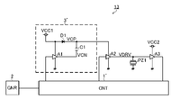
- FIG. 4 is a diagram showing a schematic configuration of an ultrasonic sensor according to the first embodiment.
- the ultrasonic sensor 13 shown in FIG. 4 has a configuration in which the control circuit 1 and the power supply circuit 3 in the ultrasonic sensor 11 shown in FIG. 1 are replaced with a control circuit 1' and a power supply circuit 3'. Similar to the ultrasonic sensors 11 and 12, the ultrasonic sensor 13 also senses the distance to the object to be measured.
- the control circuit 1' controls the drive circuit A2 based on the clock signal output from the clock signal generator 2.
- the control circuit 1' processes the output signal of the receiving circuit A3 to calculate the distance to the object to be measured.
- the control circuit 1' supplies a signal for controlling the power supply circuit 3' to the input terminal of the amplifier A1.
- the power supply circuit 3' has a configuration in which the smoothing circuit composed of the diode D2 and the capacitor C2 is removed from the power supply circuit 3. That is, the power supply circuit 3' is configured without a smoothing circuit.
- the power supply circuit 3 ′ can reduce the number of parts compared to the power supply circuit 3 . Therefore, it is possible to reduce the size and cost of the power supply circuit 3'.
- the power supply circuit 3' supplies the positive voltage VCP of the flying capacitor C1 to the power supply end of the drive circuit A2.
- the power supply circuit 3' is configured to operate so that the switching frequency of the diode D1 and the pulse drive frequency of the drive circuit A2 are different based on the signal supplied from the control circuit 1'. This can prevent the switching noise of the power supply circuit 3' from adversely affecting the signal processing of the piezoelectric element PZ1.
- the power supply circuit 3' operates so that the pulse drive of the drive circuit A2 is started after the discharge of the flying capacitor C1 is started, and the discharge of the flying capacitor C1 is finished after the pulse drive of the drive circuit A2 is finished. configured to That is, the power supply circuit 3' discharges the flying capacitor C1 only when the drive circuit A2 needs to be pulse-driven. This eliminates unnecessary switching operations of the power supply circuit 3'. Further, by limiting the discharge period in this manner, the smoothing circuit described above can be eliminated in the power supply circuit 3'.
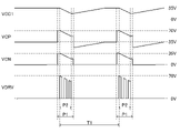
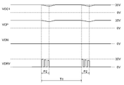
- FIG. 5 is a diagram showing waveforms of voltages of the ultrasonic sensor 13.
- FIG. 5 shows waveforms of the first constant voltage VCC1, the positive voltage VCP of the flying capacitor C1, the negative voltage VCN of the flying capacitor C1, and the drive voltage VDRV output from the drive circuit A2.
- VCC1 the first constant voltage
- VCP the positive voltage
- VCN the negative voltage
- VDRV the drive voltage
- 35 V and 70 V in FIG. 5 are merely examples, and other values may be used.
- the length of the first period P1 from the start of discharging of the flying capacitor C1 to the end of discharging of the flying capacitor C1 is the length of the second period P2 from the start of pulse driving of the drive circuit A2 to the end of pulse driving of the drive circuit A2. It is desirable to be 1 time or more and 2 times or less of . This is because if the length of the first period P1 exceeds twice the length of the second period P2, the positive electrode voltage VCP of the flying capacitor C1 may drop below the allowable value during pulse driving of the drive circuit A2. . However, the length of the first period P1 does not necessarily have to be less than twice the length of the second period P2. It is also possible to design
- the driving method of the driving circuit A2 is single-end driving, but the driving method of the driving circuit A2 may be differential driving, for example.
- the power supply circuit 3' may be a charge pump circuit, and may have a configuration other than the configuration example shown in FIG.
- the ultrasonic sensor according to the second embodiment is, like the ultrasonic sensor 14 shown in FIG. 4, an ultrasonic sensor in which the switching noise frequency of the power supply circuit does not match the pulse drive frequency of the drive circuit.
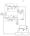
- FIG. 6 is a diagram showing a schematic configuration of an ultrasonic sensor according to the second embodiment.
- the ultrasonic sensor 14 shown in FIG. 6 includes the ultrasonic sensor 12 shown in FIG. and are added. Like the ultrasonic sensors 11-13, the ultrasonic sensor 14 also senses the distance to the object to be measured.
- the guard band clock signal GATE generated by the clock signal generator 4 is connected to the first input terminal of the AND gate AND2.
- the guard band clock signal GATE can be used to easily provide a permission period, which will be described later.
- the output signal VCOMP of the comparator COMP1 is connected to the input terminal of the NOT gate NOT1 and the second input terminal of the AND gate AND2 instead of the second input terminal of the AND gate AND1.
- the output end of the AND gate AND2 is connected to the set end of the SR flip-flop FF1.
- the output terminal of the NOT gate NOT1 is connected to the reset terminal of the SR flip-flop FF1.
- the output end of the SR flip-flop FF1 is connected to the second input end of the AND gate AND1.
- a control circuit 5 is composed of an AND gate AND2, a NOT gate NOT1, and an SR flip-flop FF1.
- the control circuit 5 is a control circuit with a simple circuit configuration including a latch circuit and a plurality of logic gates.
- the control circuit 5 is configured to permit the start of the switching operation of the diode D1 only during the permitted period provided in fixed cycles.
- the control circuit 5 is configured to permit the start of the switching operation of the diode D1 only during the period when the guard band clock signal GATE is at HIGH level.
- the control circuit 5 is configured to allow both the above-described permission period and guard band periods provided between adjacent permission periods. That is, the control circuit 5 is configured to always permit the termination of the switching operation of the diode D1. Thereby, excessive switching operation of the switch element can be suppressed.
- FIG. 7 is a diagram showing waveforms of voltages of the ultrasonic sensor 14.
- FIG. 7 shows the guard band clock signal GATE, the first constant voltage VCC1, the output voltage VOUT of the power supply circuit 3, the output signal VCOMP of the comparator COMP1, the output signal ENA of the SR flip-flop FF1, and the voltage of the flying capacitor C1.
- 3 is a diagram showing waveforms of a positive voltage VCP, a negative voltage VCN of a flying capacitor C1, and a drive voltage VDRV output from a drive circuit A2;
- FIG. A gray portion in FIG. 7 indicates a guard band period, and a white portion sandwiched between the gray portions indicates an enabled period.
- the frequencies of the positive voltage VCP of the flying capacitor C1 and the negative voltage VCN of the flying capacitor C1 during the switching operation of the diode D1 and the frequency of the pulse drive of the drive circuit A2 are shown as follows: They are the same, but usually they are very different.
- the frequencies of the positive voltage VCP of the flying capacitor C1 and the negative voltage VCN of the flying capacitor C1 are set to 10 MHz while the switching operation of the diode D1 is being performed, and the frequency of the pulse driving of the drive circuit A2 is set to 58 kHz. be done.
- the fixed period of the permission period may be set to 7 ⁇ s as shown in FIG. 8, for example.
- the frequency of the pulse drive of the drive circuit A2 and the frequency of the switching noise of the power supply circuit 3 can be made different, as shown in FIG.
- the horizontal axis in FIG. 9 indicates frequency
- the vertical axis in FIG. 9 indicates signal intensity.
- the driving method of the driving circuit A2 is single-end driving, but the driving method of the driving circuit A2 may be differential driving, for example.
- the power supply circuit 3 is not limited to a charge pump circuit, and may be a switching power supply, for example.
- the ultrasonic sensor described above can be used, for example, as an in-vehicle clearance sonar mounted on a vehicle X shown in FIG.
- the drive device for driving the piezoelectric element can be mounted in, for example, an ultrasonic flowmeter that measures the velocity of fluid, other than the ultrasonic sensor that senses the distance to the object to be measured.
- the driven element driven by the driving device is not limited to the piezoelectric element.
- the comparator COMP1 may be a hysteresis comparator.
- the power supply circuit is configured to always perform the boosting operation. 1 mode and a second mode in which the boosting operation of the power supply circuit is turned off.
- the schematic configuration of the ultrasonic sensor according to the modification of the first embodiment is similar to the schematic configuration of the ultrasonic sensor according to the first embodiment shown in FIG.
- the output of the amplifier A1 is held at 0 V in the second mode.
- the boosting operation of the power supply circuit 3 is turned off in the second mode.
- a configuration for holding the output of the amplifier A1 at 0 V in the second mode includes, for example, a configuration in which the supply of the clock signal to the amplifier A1 is stopped in the second mode, and a configuration in which the amplifier A1 outputs 0 V regardless of the input in the second mode. and the like.
- the waveform of each voltage in the first mode of the ultrasonic sensor according to the modification of the first embodiment is similar to the waveform of each voltage of the ultrasonic sensor according to the first embodiment shown in FIG.
- FIG. 11 shows waveforms of voltages in the second mode of the ultrasonic sensor according to the modification of the first embodiment.
- the piezoelectric element PZ1 can be driven to a greater extent. Therefore, in the first mode, even when the measurement object is located far from the ultrasonic sensor according to the modification of the first embodiment, the measurement object and the ultrasonic sensor according to the modification of the first embodiment distance measurement becomes possible.
- the voltage drop of the first constant voltage VCC1 becomes large after the boosting of the positive electrode voltage VCP of the flying capacitor C1 is completed, and the positive electrode voltage of the flying capacitor C1 increases. It takes time to re-boost the voltage VCP. Further, in the first mode, since the driving voltage VDRV is high, the reverberation time after driving the piezoelectric element PZ1 is long. That is, in the first mode, when the measurement object is located near the ultrasonic sensor according to the modification of the first embodiment, the measurement object and the ultrasonic sensor according to the modification of the first embodiment distance measurement becomes difficult.
- the power supply circuit 3 does not perform the boosting operation, it is not necessary to secure a waiting time until the positive electrode voltage VCP of the flying capacitor C1 is completed to be boosted again. Further, in the second mode, the drive voltage VDRV is reduced, so the reverberation time after driving the piezoelectric element PZ1 is shortened. Therefore, in the second mode, even when the measurement object is located near the ultrasonic sensor according to the modification of the first embodiment, the measurement object and the ultrasonic sensor according to the modification of the first embodiment distance measurement becomes easier.
- the situation where it is appropriate to drive the piezoelectric element PZ1 large for example, the situation where long-distance measurement is required
- the situation where it is appropriate to drive the piezoelectric element PZ1 small for example, situations where short-range measurement is required.
- the ultrasonic sensor intermittently repeats pulse driving of the piezoelectric element PZ1, and the repetition period T1 (see FIGS. 5 and 11) is set to a threshold value (for example, 10 milliseconds) or more. , the first mode is executed, and the second mode is executed when the repetition period T1 is set to be less than a threshold (eg, 10 milliseconds).
- the first mode can drive the piezoelectric element PZ1 to a low frequency and periodically increase the piezoelectric element PZ1
- the second mode can drive the piezoelectric element PZ1 to a high frequency and a periodic decrease. can be driven. Therefore, the ultrasonic sensor according to the modification of the first embodiment can be used in a situation where it is appropriate to drive the piezoelectric element PZ1 to a large extent periodically at low frequency (for example, when it is necessary to take a long period for receiving reflected waves).
- the switching frequency of the switch element and the pulse driving frequency of the driven element are the same as long as the influence of switching noise of the power supply circuit on the signal processing of the driven element is within the allowable range.
- the drive device described above includes a power supply circuit (3') including a switch element (D1), and a drive circuit configured to pulse-drive an element to be driven using a voltage supplied from the power supply circuit as a power supply voltage. (A2), wherein the power supply circuit is configured to operate such that the switching frequency of the switch element and the frequency of the pulse drive are different (first configuration).
- the driving device having the first configuration can prevent the switching noise of the power supply circuit from adversely affecting the signal processing of the element to be driven.
- the power supply circuit is a charge pump circuit including a flying capacitor (C1), the power supply circuit starts the pulse drive after the flying capacitor starts discharging, and the The configuration (second configuration) may be such that the discharge of the flying capacitor is terminated after the pulse drive is terminated.
- the power supply circuit discharges the flying capacitor only when pulse drive of the drive circuit is required. This eliminates unnecessary switching operations of the power supply circuit.
- the length of the first period from the start of discharge of the flying capacitor to the end of discharge of the flying capacitor is the second period from the start of the pulse drive to the end of the pulse drive.
- the drive device having the third configuration can prevent the positive electrode voltage of the flying capacitor from falling below the allowable value during pulse driving of the drive circuit.
- the power supply circuit may have a configuration (fourth configuration) in which a smoothing circuit is not provided at the output stage of the power supply circuit.
- the driving device having the fourth configuration can achieve miniaturization and cost reduction of the power supply circuit.
- a configuration comprising a control circuit (5) configured to allow the start of the switching operation of the switch element only during the permission period provided in a fixed period (fifth configuration) ).
- the driving device having the fifth configuration can control the length of the period during which the power supply circuit does not perform the switching operation of the switch element, thereby preventing the switching noise of the power supply circuit from adversely affecting the signal processing of the driven element. can be prevented.
- the control circuit permits termination of the switching operation of the switch element during both the permitted period and a guard band period provided between the adjacent permitted periods. It may be a configuration (sixth configuration) including a control circuit configured to.
- the driving device having the sixth configuration can suppress excessive switching operation of the switch element.
- control circuit is configured to receive the clock signal of the fixed period and set the permission period based on the clock signal (seventh configuration).
- the driving device having the seventh configuration can easily set the permission period.
- control circuit may have a configuration (eighth configuration) including a latch circuit (FF1) and a plurality of logic gates (AND2, NOT1).
- the driving device having the eighth configuration can have a control circuit with a simple circuit configuration.
- a configuration including a first mode for turning on the boosting operation of the power supply circuit and a second mode for turning off the boosting operation of the power supply circuit ( 9th configuration).
- the driving device having the ninth configuration can drive the driven element to a large extent in the first mode, and can drive the driven element to a small extent in the second mode. Therefore, the driving device having the ninth configuration can cope with both situations in which it is appropriate to drive the element to be driven large and to drive the element to be driven small.
- the drive circuit intermittently repeats the pulse drive, the first mode is executed when the cycle of repetition is equal to or greater than a threshold, and the cycle of repetition is less than the threshold.
- a configuration (tenth configuration) in which the second mode is executed may be employed.
- the first mode can drive the element to be driven to a low frequency and periodically to a large size
- the second mode can drive the element to be driven to a high frequency and periodically to a small size.
- the driving device having the ninth configuration described above can be used in a situation where it is appropriate to drive the element to be driven in a low frequency and cyclically to a large value, and in a situation in which it is appropriate to drive the element to be driven in a high frequency and cyclically to a small value. It is possible to correspond to any of the above.
- the ultrasonic sensors (13, 14) described above comprise a piezoelectric element (PZ1), a driving device having any one of the first to eighth configurations configured to drive the piezoelectric element, and a configuration (first 11).
- the ultrasonic sensor having the eleventh configuration it is possible to prevent the switching noise of the power supply circuit from adversely affecting the signal processing of the element to be driven.
Landscapes
- Engineering & Computer Science (AREA)
- Physics & Mathematics (AREA)
- Radar, Positioning & Navigation (AREA)
- Remote Sensing (AREA)
- Computer Networks & Wireless Communication (AREA)
- General Physics & Mathematics (AREA)
- Power Engineering (AREA)
- Acoustics & Sound (AREA)
- Measurement Of Velocity Or Position Using Acoustic Or Ultrasonic Waves (AREA)
Abstract
Description
図1は、第1比較例に係る超音波センサの概略構成を示す図である。図1に示す超音波センサ11は、制御回路1、クロック信号生成部2と、電源回路3と、駆動回路A2と、圧電素子PZ1と、受信回路A3と、を備える。超音波センサ11は、測定対象物までの距離をセンシングする。
超音波センサ11は、電源回路3の出力電圧が第1定電圧VCC1に依存するため電源回路3の出力電圧を任意の値に制御することができないという問題を有する。第2比較例に係る超音波センサは、当該問題を解決することができる超音波センサである。図3は、第2比較例に係る超音波センサの概略構成を示す図である。
超音波センサ12では、電源回路3がダイオードD1のスイッチング動作を行わない期間の長さが負荷電流の値、電源回路3の能力、第1定電圧VCC1の値等に依存して決まる。このため、電源回路3がダイオードD1のスイッチング動作を行う期間と電源回路3がダイオードD1のスイッチング動作を行わない期間との周期は制御できない。したがって、超音波センサ12では、電源回路3がダイオードD1のスイッチング動作を行う期間と電源回路3がダイオードD1のスイッチング動作を行わない期間との周期の逆数と、駆動回路A2のパルス駆動の周波数とが一致してしまうおそれがある。つまり、超音波センサ12では、電源回路3のスイッチングノイズの周波数と駆動回路A2のパルス駆動の周波数が一致してしまうおそれがある。
第2実施形態に係る超音波センサは、図4に示す超音波センサ14と同様に、電源回路のスイッチングノイズの周波数と駆動回路のパルス駆動の周波数とが一致しない超音波センサである。図6は、第2実施形態に係る超音波センサの概略構成を示す図である。
上述した超音波センサは、例えば図10に示す車両Xに搭載される車載用クリアランスソナーとして利用することができる。また、圧電素子を駆動する駆動装置は、測定対象物までの距離をセンシングする超音波センサ以外に、例えば流体の速度を計測する超音波流量計に搭載することもできる。
なお、本発明の構成は、上記実施形態のほか、発明の主旨を逸脱しない範囲で種々の変更を加えることが可能である。上記実施形態は、全ての点で例示であって、制限的なものではないと考えられるべきであり、本発明の技術的範囲は、上記実施形態の説明ではなく、特許請求の範囲によって示されるものであり、特許請求の範囲と均等の意味及び範囲内に属する全ての変更が含まれると理解されるべきである。
2、4 クロック信号生成部
3、3’ 電源回路
11~14 超音波センサ
A1 アンプ
A2 駆動回路
A3 受信回路
AND1、AND2 ANDゲート
C1 フライングコンデンサ
C2 コンデンサ
COMP1 コンパレータ
D1、D2 ダイオード
FF1 SRフリップフロップ
NOT1 NOTゲート
R1、R2 抵抗
REF1 基準電圧源
PZ1 圧電素子
X 車両
Claims (11)
- スイッチ素子を含む電源回路と、
前記電源回路から供給される電圧を電源電圧として用い、駆動対象素子をパルス駆動するように構成される駆動回路と、
を備え、
前記電源回路は、前記スイッチ素子のスイッチング周波数と前記パルス駆動の周波数とが異なるように動作するように構成される、駆動装置。 - 前記電源回路は、フライングコンデンサを含むチャージポンプ回路であり、
前記電源回路は、前記フライングコンデンサの放電開始以後に前記パルス駆動が開始され、前記パルス駆動の終了以後に前記フライングコンデンサの放電が終了するように動作するように構成される、請求項1に記載の駆動装置。 - 前記フライングコンデンサの放電開始から前記フライングコンデンサの放電終了までの第1期間の長さは、前記パルス駆動の開始から前記パルス駆動の終了までの第2期間の長さの1倍以上2倍以下である、請求項2に記載の駆動装置。
- 前記電源回路は、前記電源回路の出力段に平滑回路を備えない、請求項2又は請求項3に記載の駆動装置。
- 前記スイッチ素子のスイッチング動作の開始を、固定周期で設けられる許可期間のみで許可するように構成される制御回路を備える、請求項1に記載の駆動装置。
- 前記制御回路は、前記スイッチ素子のスイッチング動作の終了を、前記許可期間と、隣接する前記許可期間同士の間に設けられるガードバンド期間との双方で許可するように構成される制御回路を備える、請求項5に記載の駆動装置。
- 前記制御回路は、前記固定周期のクロック信号を受け取り、前記クロック信号に基づき前記許可期間を設けるように構成される、請求項5又は請求項6に記載の駆動装置。
- 前記制御回路は、ラッチ回路と、複数の論理ゲートと、を備える、請求項7に記載の駆動装置。
- 前記電源回路の昇圧動作をオンにする第1モードと、前記電源回路の昇圧動作をオフにする第2モードと、を備える、請求項1~8のいずれか一項に記載の駆動装置。
- 前記駆動回路は前記パルス駆動を間欠的に繰り返し、
前記繰り返しの周期が閾値以上であれば第1モードが実行され、
前記繰り返しの周期が前記閾値未満であれば第2モードが実行される、請求項9に記載の駆動装置。 - 圧電素子と、
前記圧電素子を駆動するように構成される請求項1~10のいずれか一項に記載の駆動装置と、
を備える、超音波センサ。
Priority Applications (3)
| Application Number | Priority Date | Filing Date | Title |
|---|---|---|---|
| CN202280039664.1A CN117413203A (zh) | 2021-06-03 | 2022-05-31 | 驱动装置以及超声波传感器 |
| JP2023525843A JPWO2022255341A1 (ja) | 2021-06-03 | 2022-05-31 | |
| US18/523,183 US20240094367A1 (en) | 2021-06-03 | 2023-11-29 | Drive device and ultrasonic sensor |
Applications Claiming Priority (4)
| Application Number | Priority Date | Filing Date | Title |
|---|---|---|---|
| JP2021093704 | 2021-06-03 | ||
| JP2021-093704 | 2021-06-03 | ||
| JP2021-215158 | 2021-12-28 | ||
| JP2021215158 | 2021-12-28 |
Related Child Applications (1)
| Application Number | Title | Priority Date | Filing Date |
|---|---|---|---|
| US18/523,183 Continuation US20240094367A1 (en) | 2021-06-03 | 2023-11-29 | Drive device and ultrasonic sensor |
Publications (1)
| Publication Number | Publication Date |
|---|---|
| WO2022255341A1 true WO2022255341A1 (ja) | 2022-12-08 |
Family
ID=84323396
Family Applications (1)
| Application Number | Title | Priority Date | Filing Date |
|---|---|---|---|
| PCT/JP2022/022068 Ceased WO2022255341A1 (ja) | 2021-06-03 | 2022-05-31 | 駆動装置及び超音波センサ |
Country Status (3)
| Country | Link |
|---|---|
| US (1) | US20240094367A1 (ja) |
| JP (1) | JPWO2022255341A1 (ja) |
| WO (1) | WO2022255341A1 (ja) |
Citations (6)
| Publication number | Priority date | Publication date | Assignee | Title |
|---|---|---|---|---|
| US20120163632A1 (en) * | 2010-12-23 | 2012-06-28 | John Paul Lesso | Charge pump circuit |
| WO2013137061A1 (ja) * | 2012-03-15 | 2013-09-19 | 日立アロカメディカル株式会社 | 超音波診断装置及びそのノイズ低減方法 |
| CN104180860A (zh) * | 2014-08-07 | 2014-12-03 | 湖南三一智能控制设备有限公司 | 超声波换能器盲区的控制系统与方法 |
| JP2018075142A (ja) * | 2016-11-08 | 2018-05-17 | コニカミノルタ株式会社 | 超音波診断装置の制御装置、及び制御方法 |
| US20180248477A1 (en) * | 2015-10-21 | 2018-08-30 | Chirp Microsystems, Inc. | Efficient on-chip high-voltage driver circuit for ultrasonic transducer |
| WO2022034286A1 (en) * | 2020-08-10 | 2022-02-17 | Cirrus Logic International Semiconductor Limited | Driver circuitry for capacitive transducers |
Family Cites Families (2)
| Publication number | Priority date | Publication date | Assignee | Title |
|---|---|---|---|---|
| JP5008450B2 (ja) * | 2007-04-27 | 2012-08-22 | 愛知時計電機株式会社 | 超音波流量計 |
| US8485974B2 (en) * | 2010-11-15 | 2013-07-16 | National Health Research Institutes | Multiple-frequency ultrasonic phased array driving system |
-
2022
- 2022-05-31 JP JP2023525843A patent/JPWO2022255341A1/ja active Pending
- 2022-05-31 WO PCT/JP2022/022068 patent/WO2022255341A1/ja not_active Ceased
-
2023
- 2023-11-29 US US18/523,183 patent/US20240094367A1/en active Pending
Patent Citations (6)
| Publication number | Priority date | Publication date | Assignee | Title |
|---|---|---|---|---|
| US20120163632A1 (en) * | 2010-12-23 | 2012-06-28 | John Paul Lesso | Charge pump circuit |
| WO2013137061A1 (ja) * | 2012-03-15 | 2013-09-19 | 日立アロカメディカル株式会社 | 超音波診断装置及びそのノイズ低減方法 |
| CN104180860A (zh) * | 2014-08-07 | 2014-12-03 | 湖南三一智能控制设备有限公司 | 超声波换能器盲区的控制系统与方法 |
| US20180248477A1 (en) * | 2015-10-21 | 2018-08-30 | Chirp Microsystems, Inc. | Efficient on-chip high-voltage driver circuit for ultrasonic transducer |
| JP2018075142A (ja) * | 2016-11-08 | 2018-05-17 | コニカミノルタ株式会社 | 超音波診断装置の制御装置、及び制御方法 |
| WO2022034286A1 (en) * | 2020-08-10 | 2022-02-17 | Cirrus Logic International Semiconductor Limited | Driver circuitry for capacitive transducers |
Also Published As
| Publication number | Publication date |
|---|---|
| US20240094367A1 (en) | 2024-03-21 |
| JPWO2022255341A1 (ja) | 2022-12-08 |
Similar Documents
| Publication | Publication Date | Title |
|---|---|---|
| US7965151B2 (en) | Pulse width modulator with two-way integrator | |
| EP2637294A2 (en) | Power supply device and image forming apparatus | |
| US10931204B1 (en) | Isolated resonant converter with fixed output ripple | |
| US11050345B2 (en) | Power supply apparatus and electronic control unit | |
| WO2022255341A1 (ja) | 駆動装置及び超音波センサ | |
| JP2014121015A (ja) | データ通信システム、データキャリア駆動装置、及びデータキャリア装置 | |
| KR101316667B1 (ko) | 전압 생성 회로 | |
| EP1209549A3 (en) | Voltage controller for a pulsed load, in particular for a mobile-telephone or telematics transmitter | |
| CN117413203A (zh) | 驱动装置以及超声波传感器 | |
| CN101257252B (zh) | 电压控制电路 | |
| CN116232287B (zh) | 一种同步脉冲的产生电路及电子控制单元 | |
| CN108885252B (zh) | 物体检测装置 | |
| JP3695432B2 (ja) | 流量計測装置 | |
| US20050122750A1 (en) | Synchronous rectifying type switching regulator control circuit and semiconductor integrated circuit including the same | |
| JP4994748B2 (ja) | 電源装置、電源装置を備える電子機器、電源装置を備える記録装置 | |
| WO2022190517A1 (ja) | 距離センサ | |
| JP6158775B2 (ja) | スイッチング電源装置 | |
| US9310818B2 (en) | Voltage converter and regulating circuit control chip | |
| KR101323197B1 (ko) | 디지털 소프트 스타트 회로를 이용한 컨버터 | |
| JPH048387Y2 (ja) | ||
| CN106612123B (zh) | 控制输出信号的方法和系统 | |
| US20240159886A1 (en) | Drive Device, Ultrasonic Sensor and Vehicle | |
| CN107994802A (zh) | 一种电源装置 | |
| WO2024190065A1 (ja) | 駆動装置、信号処理装置、超音波センサ、及び車両 | |
| JP2005257362A (ja) | 流れ計測装置 |
Legal Events
| Date | Code | Title | Description |
|---|---|---|---|
| 121 | Ep: the epo has been informed by wipo that ep was designated in this application |
Ref document number: 22816087 Country of ref document: EP Kind code of ref document: A1 |
|
| WWE | Wipo information: entry into national phase |
Ref document number: 2023525843 Country of ref document: JP |
|
| WWE | Wipo information: entry into national phase |
Ref document number: 202280039664.1 Country of ref document: CN |
|
| NENP | Non-entry into the national phase |
Ref country code: DE |
|
| 122 | Ep: pct application non-entry in european phase |
Ref document number: 22816087 Country of ref document: EP Kind code of ref document: A1 |