WO2022255115A1 - コイル装置および電力変換装置 - Google Patents
コイル装置および電力変換装置 Download PDFInfo
- Publication number
- WO2022255115A1 WO2022255115A1 PCT/JP2022/020815 JP2022020815W WO2022255115A1 WO 2022255115 A1 WO2022255115 A1 WO 2022255115A1 JP 2022020815 W JP2022020815 W JP 2022020815W WO 2022255115 A1 WO2022255115 A1 WO 2022255115A1
- Authority
- WO
- WIPO (PCT)
- Prior art keywords
- core
- metal base
- coil
- coil device
- wiring
- Prior art date
- Legal status (The legal status is an assumption and is not a legal conclusion. Google has not performed a legal analysis and makes no representation as to the accuracy of the status listed.)
- Ceased
Links
Images













Classifications
-
- H—ELECTRICITY
- H02—GENERATION; CONVERSION OR DISTRIBUTION OF ELECTRIC POWER
- H02M—APPARATUS FOR CONVERSION BETWEEN AC AND AC, BETWEEN AC AND DC, OR BETWEEN DC AND DC, AND FOR USE WITH MAINS OR SIMILAR POWER SUPPLY SYSTEMS; CONVERSION OF DC OR AC INPUT POWER INTO SURGE OUTPUT POWER; CONTROL OR REGULATION THEREOF
- H02M3/00—Conversion of DC power input into DC power output
- H02M3/003—Constructional details, e.g. physical layout, assembly, wiring or busbar connections
-
- H—ELECTRICITY
- H01—ELECTRIC ELEMENTS
- H01F—MAGNETS; INDUCTANCES; TRANSFORMERS; SELECTION OF MATERIALS FOR THEIR MAGNETIC PROPERTIES
- H01F27/00—Details of transformers or inductances, in general
- H01F27/08—Cooling; Ventilating
- H01F27/22—Cooling by heat conduction through solid or powdered fillings
-
- H—ELECTRICITY
- H01—ELECTRIC ELEMENTS
- H01F—MAGNETS; INDUCTANCES; TRANSFORMERS; SELECTION OF MATERIALS FOR THEIR MAGNETIC PROPERTIES
- H01F27/00—Details of transformers or inductances, in general
- H01F27/28—Coils; Windings; Conductive connections
- H01F27/2804—Printed windings
-
- H—ELECTRICITY
- H01—ELECTRIC ELEMENTS
- H01F—MAGNETS; INDUCTANCES; TRANSFORMERS; SELECTION OF MATERIALS FOR THEIR MAGNETIC PROPERTIES
- H01F27/00—Details of transformers or inductances, in general
- H01F27/28—Coils; Windings; Conductive connections
- H01F27/2876—Cooling
-
- H—ELECTRICITY
- H01—ELECTRIC ELEMENTS
- H01F—MAGNETS; INDUCTANCES; TRANSFORMERS; SELECTION OF MATERIALS FOR THEIR MAGNETIC PROPERTIES
- H01F27/00—Details of transformers or inductances, in general
- H01F27/28—Coils; Windings; Conductive connections
- H01F27/30—Fastening or clamping coils, windings, or parts thereof together; Fastening or mounting coils or windings on core, casing, or other support
- H01F27/306—Fastening or mounting coils or windings on core, casing or other support
-
- H—ELECTRICITY
- H01—ELECTRIC ELEMENTS
- H01F—MAGNETS; INDUCTANCES; TRANSFORMERS; SELECTION OF MATERIALS FOR THEIR MAGNETIC PROPERTIES
- H01F27/00—Details of transformers or inductances, in general
- H01F27/28—Coils; Windings; Conductive connections
- H01F27/2804—Printed windings
- H01F2027/2814—Printed windings with only part of the coil or of the winding in the printed circuit board, e.g. the remaining coil or winding sections can be made of wires or sheets
Definitions
- the present disclosure relates to coil devices and power conversion devices.
- power converters such as DC-DC converters are equipped with coil devices such as smoothing reactors and transformers.
- a coil device mounted on a power conversion device is composed of a coil and a core.
- the core has the function of forming a magnetic path, which is the path of the lines of magnetic force generated by the current flowing through the coil.
- a direct current or an alternating voltage is applied to the coils of the coil system.
- the heat generated by the energization of the coil device is roughly divided into Joule heat generated in the coil and heat generated in the core. Joule heating increases in inverse proportion to the cross-sectional area of the wiring used as the coil. For this reason, if wiring with a small cross-sectional area is used to reduce the size of the coil device, Joule heat generated in the coil device will increase.
- the skin effect causes the current to flow only in the vicinity of the surface of the wiring, increasing the electrical resistance of the coil device. As the frequency of the alternating current flowing through the wiring increases, the electrical resistance increases monotonously.
- the frequency of the AC voltage applied to the coil device is set to a higher value in an attempt to reduce the size of the coil device, the electric resistance value of the wiring of the coil device increases due to the skin effect. Joule heating will increase.
- the coil device in order to keep the temperature of the coil device from rising due to Joule heat generated in the coil device, the coil device is required to have improved heat dissipation properties. That is, in order to reduce the size of the coil device, it is also required to improve the heat dissipation of the coil device.
- a technique is proposed in which heat generated from the coil, particularly in the inner region of the core, is dissipated through the printed circuit board and the coil.
- the present disclosure has been made as part of such development, and one object is to provide a coil device capable of improving heat dissipation, and another object is to provide such a coil device. It is to provide an applied power converter.
- a coil device is a coil device having one or more coil units.
- the coil unit has a core and a first winding portion.
- the core has one or more looped magnetic paths.
- the first winding portion is wound on the core in such a manner as to pass through an inner region of the core surrounded by the core.
- a metal base substrate having a coil pattern formed on a metal base body with an insulating layer interposed is disposed in the inner region of the core and the outer region of the core.
- a first through hole through which the core penetrates is formed in the metal base substrate.
- a cooling body is thermally bonded to the metal base main body on the side opposite to the side on which the insulating layer and the coil pattern are formed.
- the first winding portion includes a coil pattern.
- a power conversion device includes the coil device described above.
- heat generated in the portion of the first winding portion located in the outer region of the core is radiated to the cooling body via the insulating layer and the metal base body. Further, heat generated in the portion of the first winding portion located in the inner region of the core is also dissipated to the cooling body via the insulating layer and the metal base body. As a result, the heat generated in the portion of the first winding portion located in the inner region of the core is dissipated to the cooling body to the same extent as the heat generated in the portion of the first winding portion located in the outer region of the core. can be made As a result, the heat dissipation of the coil device can be improved.
- heat dissipation can be improved by including the coil device described above.
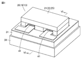
- FIG. 1 is an exploded perspective view showing an example of a coil device according to Embodiment 1;
- FIG. 3 is a perspective view of the coil device shown in FIG. 2 in the embodiment;
- FIG. FIG. 4 is an exploded perspective view showing the structure of the metal base substrate in the coil device in the embodiment;
- FIG. 5 is a diagram for explaining the reason why slits are provided in the metal base substrate in the same embodiment;
- FIG. 4 is a cross-sectional view along the cross-sectional line VI-VI shown in FIG. 3 in the same embodiment;
- it is a cross-sectional view showing an example of a coil device according to a first example of a first modification.
- FIG. 1 it is a cross-sectional view showing an example of a coil device according to a second example of the first modification.
- it is a sectional view showing an example of the coil device concerning the 2nd modification.
- it is a sectional view showing an example of the coil device concerning the 3rd modification.
- it is an exploded perspective view showing an example of a coil device concerning a 4th modification.
- it is a figure which shows the variation of arrangement
- FIG. 11 is a diagram for explaining an induced current formed in a cooling body assumed in a coil device according to a fifth modification in the same embodiment;
- FIG. 4 is a diagram showing an example of steps of a method for manufacturing a coil device in the same embodiment; In the same embodiment, it is a perspective view showing an example of a coil device according to a seventh modification.
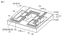
- FIG. 17 is a cross-sectional view along the cross-sectional line XVII-XVII shown in FIG. 16 in the same embodiment; In the embodiment, it is a perspective view showing an example of a coil device according to an eighth modification.
- FIG. 19 is a cross-sectional view along the cross-sectional line XIX-XIX shown in FIG.
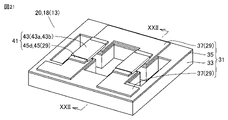
- FIG. 18 is a perspective view showing an example of a coil device according to a ninth modification.
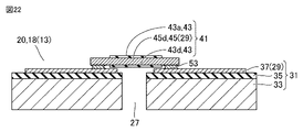
- FIG. 22 is a cross-sectional view along the cross-sectional line XXII-XXII shown in FIG. 21 in the same embodiment;
- FIG. 21 is an exploded perspective view showing an example of a coil device according to a twelfth modification in the same embodiment;
- it is a perspective view showing an example of a coil device according to a thirteenth modification.
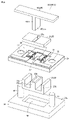
- FIG. 21 is an exploded perspective view showing an example of a coil device according to a sixteenth modification in the same embodiment; In the embodiment, it is a perspective view showing an example of a coil device according to a seventeenth modification.
- FIG. 20 is a cross-sectional view showing an example of a coil device according to an eighteenth modification in the same embodiment;
- FIG. 11 is a perspective view for explaining an example of a coil device according to Embodiment 2; It is a perspective view which shows a coil apparatus in the same embodiment.
- FIG. 21 is an exploded perspective view showing an example of a coil device according to a sixteenth modification in the same embodiment.
- FIG. 20 is a cross-sectional view showing an example of a coil device according to an eighteenth modification in the same embodiment
- FIG. 11 is a perspective view for explaining an example of a coil device according to Embodiment 2; It is a perspective view which shows a coil apparatus in the same embodiment.
- FIG. 33 is a cross-sectional view along the cross-sectional line XXXIII-XXXIII shown in FIG. 32 in the same embodiment;
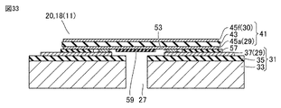
- FIG. 33 is a cross-sectional view along the cross-sectional line XXXIV-XXXIV shown in FIG. 32 in the same embodiment;
- FIG. 11 is a perspective view showing an example of a coil device according to Embodiment 3;
- FIG. 36 is a cross-sectional view along the cross-sectional line XXXVIa-XXXVIa or the cross-sectional line XXXVIb-XXXVIb shown in FIG. 35 in the embodiment;
- it is a perspective view showing an example of a coil device according to a modification.
- FIG. 1 shows an example of a circuit diagram of a DC-DC converter.
- a DC-DC converter is mounted, for example, on an electric vehicle.
- the DC-DC converter has a function of converting an input voltage of about 100V to 300V of the lithium ion battery into a voltage of 12V to 15V and outputting the converted voltage to charge the lead storage battery.
- the DC-DC converter as the power conversion device 1 includes an inverter circuit unit 2, a transformer unit 3, a rectifier circuit unit 4, a smoothing circuit unit 5, an input terminal 6, an input capacitor 8, a control circuit unit 10 and an output terminal 7 .
- the inverter circuit section 2 is composed of switching elements 9, and here, is composed of four switching elements 9a, 9b, 9c and 9d.
- the switching element 9 for example, a power semiconductor element such as a MOS transistor (MOSFET: Metal Oxide Semiconductor Field Effect Transistor) or an insulated gate bipolar transistor (IGBT: Insulated Gate Bipolar Transistor) is applied.
- MOSFET Metal Oxide Semiconductor Field Effect Transistor
- IGBT Insulated Gate Bipolar Transistor
- the transformer section 3 is composed of a transformer 11 having a primary winding 11a and a secondary winding.
- the rectifier circuit section 4 is composed of a rectifier element 12, and here is composed of two rectifier elements 12a and 12b.
- a power semiconductor element such as a diode, a MOS transistor, or a thyristor is applied as the rectifying element 12, for example.
- the smoothing circuit section 5 is composed of a smoothing reactor 13 and a smoothing capacitor 14 .
- the switching operation of each of the four switching elements 9 in the inverter circuit unit 2 is controlled by the control circuit unit 10, so that the DC voltage input from the input terminal 6 is changed to the AC voltage. is converted to
- the AC voltage converted in the inverter circuit section 2 is converted into an arbitrary voltage by the transformer 11 .
- the voltage to be converted is determined by the turns ratio between the primary winding 11 a and the secondary winding 11 b in the transformer 11 .
- the transformer 11 electrically insulates between the input terminal 6 and the output terminal 7 .
- the AC voltage supplied from the transforming section 3 is again converted into a DC voltage by the rectifying element 12.
- smoothing circuit section 5 the DC voltage converted by rectifying circuit section 4 is smoothed by smoothing reactor 13 and smoothing capacitor 14 . As a result, the output voltage output from the output terminal 7 is stabilized.
- the transformer 11 and the smoothing reactor 13 are coil devices that generate a relatively large amount of heat. It is necessary to dissipate the heat generated in the transformer 11 and the smoothing reactor 13 and lower the temperature of each of the transformer 11 and the smoothing reactor to below the permissible temperature, for example, about 100° C. to 120° C. or less.
- a structure for dissipating heat from a coil device composed of one or more coil units will be specifically described.
- Embodiment 1 describes a smoothing reactor as an example of a coil device.
- the coil device 20 is composed of one coil unit 18.
- a smoothing reactor 13 as a coil device 20 is formed of a core 21 having one or more loop-shaped magnetic paths and a first winding portion 29 wound around the core 21 .
- the first winding portion 29 includes a coil pattern 37 on the metal base substrate 31 and a wiring body 45 on the wiring member 41 .
- the smooth reactor 13 has a metal base substrate 31 , a wiring member 41 , a core 21 and a cooling body 39 .
- the metal base substrate 31 is composed of a metal base body 33 , an insulating layer 35 and a coil pattern 37 .
- Core 21 is composed of an E-shaped core 23 and an I-shaped core 25 .
- the E-shaped core 23 has legs 23a, 23b and 23c.
- the I-shaped core 25 abuts on the leg portions 23a, 23b, and 23c, thereby forming the core 21 having a loop-shaped magnetic path.
- the E-shaped core 23 and the I-shaped core 25 are fixed with an adhesive (not shown).
- a ferrite core such as a manganese-zinc (Mn--Zn)-based ferrite core or a nickel-zinc (Ni--Zn)-based ferrite core is applied.
- an amorphous core or an iron dust core may be applied.
- the core 21 has a structure in which the E-shaped core 23 and the I-shaped core 25 are combined.
- the core is not limited to the core 25, and may be, for example, a core combining two U-shaped cores.
- the core may be a combination of two E-shaped cores.
- the core may be a combination of a T-shaped core and a U-shaped core.
- a coil pattern 37 is arranged on a metal base body 33 with an insulating layer 35 interposed therebetween.
- the metal base body 33 has a thermal conductivity of 1.0 W/(m ⁇ K) or more, preferably 10.0 W/(m ⁇ K) or more, and more preferably 100.0 W/(m ⁇ K) or more.
- the metal base body 33 is made of a metal material such as copper, iron, aluminum, iron alloy, or aluminum alloy.
- the metal base body 33 has a first major surface 33a and a second major surface 33b.
- the first major surface 33 a faces the insulating layer 35 .
- the second main surface 33 b faces the cooling body 39 .
- the metal base body 33 is formed with through holes 32 as first through holes through which the leg portions 23a, 23b and 23c of the E-shaped core 23 are respectively inserted.
- a slit 27 is formed in a portion of the metal base body 33 located between the through hole 32 through which the leg portion 23a is inserted and the through hole 32 through which the leg portion 23c is inserted.
- the slit 27 is formed in a portion of the metal base body 33 located inside the core 21 surrounded by the E-shaped core 23 and the I-shaped core 25 . In the slit 27, the end face 33c of the metal base body 33 is exposed in a facing manner.
- the portion of the metal base body 33 that surrounds the leg portion 23c of the E-shaped core 23 around which the coil pattern 37 is wound is physically and electrically separated by the slit 27. Assuming that the distance between one end face 33c and the other end face 33c is the width of the slit 27, the width of the slit 27 is set within a range of, for example, approximately 0.1 mm or more and 10 mm or less.
- the slit 27 has a function of preventing the metal base body 33 from forming a short coil. By not forming a short coil in the metal base body 33, the coil device 20 can function as the coil device 20 (smoothing reactor 13).
- the metal base is positioned so as to surround the leg portion 23c (see FIG. 2) around which the coil pattern 37 is wound.
- the parts of the main body 33 are physically and electrically connected.
- the insulating layer 35 has a first main surface 35a and a second main surface 35b.
- the second main surface 35b is arranged in a state in which it contacts substantially the entire surface of the first main surface 33a of the metal base body 33 .
- the insulating layer 35 has electrical insulation.
- the insulating layer 35 is made of, for example, epoxy resin, glass fiber reinforced epoxy resin, or polyimide resin.
- a thermally conductive filler may be mixed into the epoxy resin or the like.
- the thickness of the insulating layer 35 is preferably as thin as possible within a range that does not affect electrical insulation or manufacturability.
- the thickness of the insulating layer 35 is set to, for example, approximately 1 ⁇ m or more and 2000 ⁇ m or less. More preferably, the thickness of the insulating layer 35 is set to approximately 1 ⁇ m or more and 200 ⁇ m or less.
- a coil pattern 37 is arranged on the first main surface 35 a of the insulating layer 35 .
- the insulating layer 35 is formed with through holes 32 through which the leg portions 23a, 23b and 23c of the E-shaped core 23 are inserted.
- the insulating layer 35 may have a pattern that straddles the slits 27 formed in the metal base body 33 . In this case, it is preferable to secure the strength of the insulating layer 35 .
- the coil pattern 37 is formed in such a manner that it is in close contact with the first main surface 35a of the insulating layer 35 .
- a wiring pattern (not shown) other than the coil pattern 37 may be formed on the first main surface 35 a of the insulating layer 35 .
- the thickness of the coil pattern 37 and the like is, for example, approximately 1 ⁇ m or more and 2000 ⁇ m or less.
- the coil pattern 37 and the like are made of copper, nickel, gold, aluminum, silver, tin, or the like, for example. Also, the coil pattern 37 and the like may be made of an alloy containing these metals.
- the insulating layer 35 is arranged so as to contact substantially the entire surface of the first main surface 33 a of the metal base body 33 . Heat generated in the coil pattern 37 is radiated to the metal base body 33 through the insulating layer 35 .
- the thickness of the insulating layer 35 By setting the thickness of the insulating layer 35 as thin as possible within a range that does not affect both electrical insulation and manufacturability, the heat dissipation of the heat dissipation path can be enhanced.
- the coil pattern 37 and the end surface 33c of the metal base body 33 are separated by a creeping distance CR.
- a creeping distance CR By ensuring the creepage distance CR, when the potential of the coil pattern 37 and the potential of the metal base body 33 are different, dielectric breakdown occurs on the creepage surface between the coil pattern 37 and the end face 33c of the metal base body 33. can be prevented.
- the creepage distance CR is set based on the potential of the coil pattern 37 and the potential of the metal base body 33 . As the potential difference between the potential of the coil pattern 37 and the potential of the metal base body 33 increases, it is necessary to set the creepage distance CR longer. From the viewpoint of preventing dielectric breakdown, it is preferable that the coil pattern 37 has, for example, a rounded pattern so that there are no sharp corners or the like as much as possible.
- the wiring member 41 includes a coil pattern 37 arranged in one portion of the metal base body 33 divided by the slit 27 and a coil pattern 37 arranged in the other portion. arranged to be electrically connected.
- a printed circuit board is applied as the wiring member 41 .
- the wiring member 41 for example, a metal bus bar or the like covered with an insulating film may be applied in addition to the printed circuit board.
- the wiring member 41 has an insulating portion 43 and a wiring body 45 .
- the wiring body 45 is formed on the side facing the coil pattern 37 in the insulating portion 43 .
- the wiring body 45 is made of, for example, copper, nickel, gold, aluminum, silver, tin, or the like, like the coil pattern 37 and the like.
- the insulating portion 43 has electrical insulation.
- the insulating portion 43 is made of, for example, glass fiber reinforced epoxy resin, phenol resin, polyphenylene sulfide (PPS), polyether ether ketone (PEEK), or the like.
- the printed circuit board applied as the wiring member 41 may be made of a material generally considered to have relatively low thermal conductivity. That is, the printed circuit board applied to the wiring member 41 may be a general-purpose printed circuit board. Moreover, as a printed circuit board applied to the wiring member 41, a ceramic substrate such as aluminum oxide, aluminum nitride, or silicon carbide may be applied. A conductive portion (not shown) may be formed on or inside the wiring member 41 .
- the wiring member 41 for example, a laminated bus bar obtained by laminating an insulating film sheet and a metal conductor may be used.
- an insulating film sheet for example, a film made of polyethylene terephthalate (PET), a film made of polyimide (PI), or paper made of aramid (wholly aromatic polyamide) fiber applies.
- PET polyethylene terephthalate
- PI polyimide
- aramid whole aromatic polyamide
- the wiring main body 45 of the wiring member 41 is electrically connected to the coil pattern 37 via the joint member 53 .
- the joint member 53 is made of a conductive material.
- a conductive adhesive, solder, or the like, for example, can be applied as the joining member 53 .
- the wiring member 41 and the metal base substrate 31 are thermally coupled via the joining member 53 so as to be heat conductive.
- a heat conducting member 57 as a first heat conducting member between the coil pattern 37 and the wiring body 45 .
- the wiring member 41 and the metal base substrate 31 are thermally coupled via the heat conducting member 57 in addition to the joining member 53 so that heat can be conducted.
- the thermal conductivity of the heat conducting member 57 is, for example, preferably 0.1 W/(mK) or more, more preferably 1.0 W/(mK) or more, and 10.0 W/(mK) or more. is more preferred.
- heat-conducting member 57 for example, heat-conducting grease, a heat-conducting sheet, a heat-conducting adhesive, or the like can be applied.
- the metal base substrate 31 on which the coil pattern 37 is formed is placed on the cooling body 39 .
- the metal base substrate 31 is fixed to the cooling body 39 with screws (not shown).
- the cooling body 39 has a groove portion 40 formed in a main surface 39 a facing the metal base body 33 .
- the E-shaped core 23 is accommodated in the groove portion 40 .
- the thermal conductivity of the cooling body 39 is, for example, preferably 1.0 W/(mK) or more, more preferably 10.0 W/(mK) or more, and 100.0 W/(mK) or more. More preferred.
- the cooling body 39 is made of metal material such as copper, iron, aluminum, iron alloy or aluminum alloy. Also, the cooling body 39 may be made of, for example, a resin having a high thermal conductivity. Note that the cooling body 39 may be electrically connected to other members so as to have the same potential as the ground potential.
- the main surface 39a of the cooling body 39 is in contact with the second main surface 33b (see FIG. 4) of the metal base body 33, so that the cooling body 39 and the metal base body 33 (metal base substrate 31) can conduct heat. is thermally coupled to By interposing a heat-conducting member (not shown) between the main surface 39a of the cooling body 39 and the second main surface 33b of the metal base body 33, heat can be more easily conducted.
- the cooling body 39 is in contact with the E-shaped core 23 (core 21) on the bottom surface of the groove 40, so that the core 21 and the cooling body 39 are thermally coupled so as to be heat conductive.
- a heat-conducting member (not shown) between the groove portion 40 of the cooling body 39 and the E-shaped core 23, heat can be more easily conducted.
- the E-shaped core 23 and the cooling body 39 may be adhered with an adhesive (not shown) or the like. Also, the cooling body 39 may constitute a part of the housing of the coil device 20 . Moreover, the cooling body 39 may constitute a part of the housing of the power conversion device 1 including the coil device 20 . Furthermore, a surface of the cooling body 39 other than the surface on which the metal base substrate 31 is arranged may be air-cooled or water-cooled.
- an insulating member 59 may be arranged so as to cover the portion of the wiring body 45 of the wiring member 41 located above the slit 27 (first example). Moreover, as shown in FIG. 8, an insulating member 59 may be arranged so as to cover the slit 27 (second example).
- the insulating member 59 may be made of an electrically insulating material.
- an adhesive tape obtained by applying a silicon-based adhesive to a polyimide tape may be applied.
- the distance (spatial distance) between the wiring main body 45 and the metal base main body 33 can be increased by arranging the insulating member 59 .
- the occurrence of dielectric breakdown in the region (space) between the wiring body 45 and the metal base body 33 can be more effectively prevented. can be prevented.
- a wiring body 45a is formed on the surface (lower surface) of the insulating portion 43 facing the metal base substrate 31, and the surface of the insulating portion 43 facing the metal base substrate 31 is A wiring member 41 having a wiring main body 45b formed on the opposite surface (upper surface) may be applied.
- the wiring main bodies 45 a and 45 b are electrically connected by a through-hole conductive portion 47 formed so as to penetrate the insulating portion 43 .
- the insulating member 59 shown in FIG. 7 or 8 may be arranged.
- the wiring main body 45a may be formed in such a manner that the portion positioned directly above the slit 27 is excluded from the surface of the insulating portion 43 facing the metal base substrate 31 .
- the wiring main body 45a and the metal base can be connected without arranging the insulating member 59 shown in FIG. A distance (spatial distance) to the main body 33 can be secured.
- the wiring member 41 having the structure shown in FIG. 10 may be applied as the coil device 20 shown in FIG.
- the core 21 and the metal base substrate 31 may be fixed together with a fixing tape 61.
- a fixing tape 61 for example, an adhesive tape obtained by applying an acrylic adhesive to a polyester film can be applied.
- the dimensions of each part including the groove 40 are set so that the fixing tape 61 that fixes the core 21 and the metal base substrate 31 does not interfere with the cooling body 39 .
- Metal base substrate 31 is fixed to cooling body 39 by screws (not shown), for example.
- FIG. 12 shows a second arrangement example and a third arrangement example in addition to the first arrangement example shown in FIG.
- the metal base body 33 is divided into a metal base body 34a and a metal base body 34b in plan view.
- the metal base main body 34 a and the metal base main body 34 b are arranged with a gap therebetween, and this gap functions as the slit 27 .
- a slit 27 is formed in the metal base body 34a so as to communicate the through hole 32 and the outer region of the metal base body 34a.
- a slit 27 is formed in the metal base body 34b so as to communicate the through hole 32 with the outer region of the metal base body 34b.
- the metal base body 34a and the metal base body 34b may be connected to each other by, for example, a connection member (not shown). Also, each of the metal base body 34a and the metal base body 34b may be fixed to the cooling body 39 (see FIG. 2) by screws (not shown) or the like.
- slits 27 are formed to communicate each of the three through-holes 32 with the outer region of the metal base body 33 in plan view.
- FIG. 13 shows a first arrangement example, a second arrangement example, and a third arrangement example as arrangement positions of the slits 27 formed in the metal base main body 33 .
- the slit 27 is formed in such a manner that the two through-holes 32 communicate with each other in plan view.
- a slit 27 is formed that communicates between each of the two through holes 32 and the outer region of the metal base body 33 in plan view.
- the slits 27 are formed in a direction crossing the longitudinal direction of the through holes 32 .
- slits 27 are formed along the longitudinal direction of through holes 32 .
- the metal base body 33 of the metal base substrate 31 is placed on the cooling body 39 .
- the cooling body 39 is made of a conductive material such as metal, the metal base main body 33 and the cooling body 39 are electrically connected. Therefore, even if the slit 27 is formed in the metal base body 33, the induced current RP flows in a loop through the cooling body 39, and the induced current RP becomes a short coil.
- FIG. 14 it is assumed that an induced current RP1, an induced current RP2, and an induced current RP3 are formed in each of the second arrangement example and the third arrangement example.
- the cooling body 39 from an electrically insulating material such as a resin having a relatively high thermal conductivity. can.
- the coil device 20 is manufactured through a metal base substrate processing step ST1, a component mounting step ST2, and an assembly step ST3.
- the coil pattern 37 is formed on the metal base body 33 with the insulating layer 35 interposed therebetween. Furthermore, through holes 32 and slits 27 are formed in the metal base substrate 31 .
- the joint members 53 and the wiring members 41 are arranged at appropriate positions on the metal base substrate 31.
- the wiring member 41 (wiring body 45 ) is joined to the metal base substrate 31 (coil pattern 37 ) by reflow soldering or the like.
- the metal base substrate 31, the E-shaped core 23, the I-shaped core 25, and the cooling body 39 to which the wiring member 41 is joined are combined while being fixed to each other by, for example, an adhesive.
- the metal base substrate 31, the E-shaped core 23 and the I-shaped core 25 may be fixed using a fixing tape 61 (see FIG. 11).
- the coil device 20 is completed.
- the coil device 20 includes a metal base substrate 31 , wiring members 41 , cores 21 and cooling bodies 39 .
- the core 21 is formed by combining an E-shaped core 23 and an I-shaped core 25 so as to form a loop.
- the metal base substrate 31 is formed with through holes 32 through which the leg portions 23a, 23b, and 23c of the E-shaped core 23 are inserted.
- the metal base substrate 31 has a metal base body 33 , an insulating layer 35 and a coil pattern 37 .
- the metal base body 33 and the coil pattern 37 are electrically insulated by the insulating layer 35 .
- the coil pattern 37 is arranged so as to pass through a space (region) surrounded by the E-shaped core 23 and the I-shaped core 25 . That is, the coil pattern 37 is arranged so as to pass through the inner region of the core 21 .
- a slit 27 is formed in the metal base substrate 31 (metal base body 33 ) so that a short coil is not formed with respect to the core 21 .
- a wiring member 41 electrically connects the coil pattern 37 arranged on one side of the metal base substrate 31 with the slit 27 interposed therebetween and the coil pattern 37 arranged on the other side.
- the wiring member 41 is electrically connected to the coil pattern 37 by a joint member 53 .
- the cooling body 39 is formed with a groove 40 in which the core 21 (E-shaped core 23) is accommodated.
- the second main surface 33b of the metal base body 33 and the main surface 39a of the cooling body 39 are in contact with each other, and the metal base body 33 and the cooling body 39 are thermally coupled.
- heat generated from the portion of the coil pattern 37 arranged in the outer region of the core 21 is radiated to the cooling body 39 via the insulating layer 35 and the metal base main body 33 .
- the heat generated from the portion of the coil pattern 37 arranged in the inner region of the core 21 is also dissipated to the cooling body 39 via the insulating layer 35 and the metal base body 33 .
- heat dissipation from the portion of the coil pattern 37 arranged in the inner region of the core 21 is about the same as that of heat produced from the portion of the coil pattern 37 arranged in the outer region of the core 21. improve to
- the wiring member 41 (wiring main body 45) and the metal base substrate 31 (coil pattern 37) are thermally coupled via the bonding member 53. Therefore, the heat generated in the wiring member 41 (wiring main body 45 ) is radiated to the cooling body 39 via the joining member 53 , the coil pattern 37 , the insulating layer 35 and the metal base main body 33 .
- the length of the wiring body 45 (wiring member 41) electrically connecting with the coil pattern 37 is also shortened.
- heat generated near the center in the extending direction of the wiring body 45 (wiring member 41) is dissipated to the cooling body 39 via the joining member 53, the coil pattern 37, the insulating layer 35, and the metal base body 33. shorter route.
- the temperature rise in the vicinity of the center of the wiring member 41 in the extending direction can be suppressed.
- a thermally conductive member 57 is filled between the wiring member 41 (wiring main body 45) and the metal base substrate 31 (coil pattern 37). Therefore, heat generated in the wiring member 41 (wiring main body 45 ) is efficiently radiated to the cooling body 39 also via the heat conducting member 57 , the coil pattern 37 , the insulating layer 35 and the metal base main body 33 . This eliminates the need to increase the size of the pattern of the wiring member 41 in order to efficiently dissipate the heat generated in the wiring member 41 (wiring main body 45). 1 can contribute to miniaturization.
- a heat conducting member (not shown) is interposed between the metal base substrate 31 (metal base body 33) and the cooling body 39, and the core 21 (E-shaped core 23) and the cooling body 39 (groove 40) A heat conducting member (not shown) may be interposed between them.
- heat generated in the wiring member 41 (wiring main body 45 ) and radiated to the metal base main body 33 is more efficiently radiated to the cooling body 39 .
- the need to increase the size of the coil pattern 37 and the pattern of the wiring member 41 for heat radiation is further eliminated, which contributes to the miniaturization of the coil device 20 and, in turn, the miniaturization of the power conversion device 1.
- a section may be provided in which the coil pattern 37 and the wiring main body 45 are electrically connected in parallel.
- the section between the position P1 and the position P2 and the section between the position P3 and the position P4 In each of the sections and the section between the positions P5 and P6, the wiring body 45 and the coil pattern 37 electrically connected in parallel are arranged.
- the coil pattern 37 and the wiring body 45 are electrically connected by a joint member 53 .
- the wiring body 45 includes a wiring body 45 a formed on the lower surface of the insulating layer 35 and a wiring body 45 b formed on the upper surface of the insulating layer 35 .
- the wiring body 45 a and the wiring body 45 b are electrically connected via the through-hole conductive portion 47 .
- the wiring body 45 becomes part of the first winding portion 29 in addition to the coil pattern 37 .
- the cross-sectional area of the current flowing through the first winding portion 29 increases, and the Joule heat generated in the first winding portion 29 can be reduced.
- the need to increase the size of the coil pattern 37 for heat dissipation is further eliminated, which contributes to the miniaturization of the coil device 20 and thus the miniaturization of the power conversion device 1 .
- a heat conducting member 57 may be interposed between the coil pattern 37 and the wiring body 45.
- the heat generated in the wiring member 41 (wiring main body 45 ) is efficiently radiated to the cooling body 39 via the heat conducting member 57 , the coil pattern 37 , the insulating layer 35 and the metal base main body 33 .
- the heat conducting member 57 is efficiently radiated to the cooling body 39 via the heat conducting member 57 , the coil pattern 37 , the insulating layer 35 and the metal base main body 33 .
- the size of the coil device 20 can be reduced. 1 can contribute to miniaturization.
- the wiring member 41 a structure in which one printed circuit board having the wiring main body 45 formed on both sides of the insulating portion 43 is arranged is taken as an example. may apply.
- the one printed circuit board and the other printed circuit board are the wiring main body formed on the upper surface of the insulating portion of the one printed circuit board and the wiring formed on the lower surface of the insulating portion of the other printed circuit board.
- the main body is electrically connected by the joining member.
- the wiring member 41 for example, a multilayer printed circuit board in which insulating portions and wiring bodies are alternately laminated may be applied. By applying such a multilayer printed circuit board, it is possible to expand the area of the region where the wiring main body, which is part of the first winding portion 29, is arranged on the surface or inside the insulating portion. If the wiring member 41 is, for example, a two-layer printed circuit board, the area of the region where the wiring main body can be formed is approximately doubled compared to the case of a one-layer printed circuit board.
- the cross-sectional area of the current flowing through the wiring body, which is a part of the first winding portion 29, increases, and the Joule heat generated in the first winding portion 29 can be further reduced.
- the need to increase the size of the coil pattern 37 for heat dissipation is further eliminated, which contributes to the miniaturization of the coil device 20 and thus the miniaturization of the power conversion device 1 .
- a wiring member having a conductive portion electrically insulated from the wiring main body is applied to the insulating portion, and the conductive portion is thermally bonded to the cooling body 39 via the metal base substrate 31.
- a conductive portion 45c electrically insulated from the wiring main body 45a is formed on the lower surface of the insulating portion 43.
- a conductive portion 45c electrically insulated from the wiring main body 45b is formed on the upper surface of the insulating portion 43.
- a conductive portion 45 c formed on the upper surface of the insulating portion 43 and a conductive portion 45 c formed on the lower surface of the insulating portion 43 are thermally coupled by a through-hole conductive portion 49 .
- the conductive portion 45c formed on the lower surface of the insulating portion 43 is joined by a joining member 55 to the wiring pattern 37a formed on the insulating layer 35 of the metal base substrate 31. As shown in FIG.
- the wiring pattern 37 a is electrically insulated from the coil pattern 37 .
- the heat generated in the wiring bodies 45a and 45b is radiated to the cooling body 39 via the heat conducting member 57 and the metal base board 31, and is insulated from the wiring bodies 45a and 45b. Heat is radiated to the cooling body 39 via the portion 43 , the conductive portion 45 c , the joint member 55 , the wiring pattern 37 a , the insulating layer 35 and the metal base body 33 .
- the heat generated in the wiring main bodies 45a and 45b can be more efficiently dissipated to the cooling body 39. As a result, there is no need to increase the size of the pattern of the wiring member 41 for heat radiation.
- the wiring main body 45 (wiring main body 45 a, wiring main body 45 b ) in the wiring member 41 constitutes part of the first winding portion 29 .
- the wiring body 45 is wound twice around the leg portion 23c (see FIG. 2) of the E-shaped core 23 (the number of turns is 2 (2 turns)).
- the wiring body 45 and the coil pattern 37 are electrically connected in parallel by the joining member 53 (see FIG. 17). It is connected. As a result, the current flows through the wiring body 45 and the coil pattern 37 in parallel. In this way, the number of turns of the first winding portion 29 can be increased, contributing to miniaturization of the core 21 (the E-shaped core 23 and the I-shaped core 25). As a result, it is possible to contribute to miniaturization of the coil device 20 and thus miniaturization of the power conversion device 1 .
- the wiring member 41 the structure in which one printed circuit board having the wiring main body 45 formed on both sides of the insulating portion 43 is arranged is taken as an example, but the wiring member 41 in which two or more printed circuit boards are laminated can be used. may apply.
- the one printed circuit board and the other printed circuit board are the wiring main body formed on the upper surface of the insulating portion of the one printed circuit board and the wiring formed on the lower surface of the insulating portion of the other printed circuit board.
- the main body is electrically connected by the joining member.
- the wiring member 41 for example, a multi-layer printed circuit board in which insulating portions and wiring bodies are alternately laminated may be applied.
- the number of turns of the first winding portion 29 (wiring main body 45 ) can be increased, which can contribute to miniaturization of the core 21 .
- a metal bus bar may be applied as the wiring member.
- the wiring member 41 includes a metal bus bar 45d that serves as a wiring body 45, and insulating portions 43a and 43b that cover the metal bus bar 45d.
- the insulating portion 43a is formed in such a manner that a portion of the upper surface of the metal bus bar 45d is exposed.
- the insulating portion 43b is formed so as to expose a portion of the lower surface of the metal bus bar 45d.
- the metal bus bar 45d and the coil pattern 37 are electrically connected. A portion of the exposed lower surface of the metal bus bar 45 d and the coil pattern 37 are joined by a joining member 53 .
- the metal bus bar 45d is made of a metal such as copper, like the other wiring bodies 45. As shown in FIG.
- the thickness of metal bus bar 45d is preferably, for example, about 0.1 mm or more and 5.0 mm or less.
- the insulating portions 43a and 43b may be made of an electrically insulating material, such as epoxy resin or polyimide resin.
- the insulating portion 43b is formed between one joint member 53 and the other joint member 53 so as to cover the portion of the lower surface of the metal bus bar 45d located directly above the slit 27. As shown in FIG.
- the insulating portion 43b has a function of preventing dielectric breakdown from occurring in a region (space) between the metal bus bar 45d and the metal base body 33. As shown in FIG.
- the thickness of the metal bus bar 45d can be easily increased compared to the wiring body 45 formed on the surface of the insulating portion 43 of the printed circuit board. Therefore, by setting the thickness of the metal bus bar 45d as the wiring main body 45 to be thicker than the thickness of the wiring main body 45 in the printed circuit board, the current path cross-sectional area through which the current flows can be increased. Thereby, Joule heat generated in the metal bus bar 45d (wiring main body 45) can be reduced. As a result, there is no need to increase the size of the pattern of the wiring member 41 for heat radiation.
- a bent metal bus bar 45e may be applied.
- Metal bus bar 45 e is bent (or curved) in a direction away from slit 27 .
- the distance between the metal bus bar 45e and the metal base body 33 is increased, and the occurrence of dielectric breakdown in the region (space) between the metal bus bar 45e and the metal base body 33 can be effectively prevented. can.
- the electrical insulation of the coil device 20 can be improved, and the electrical insulation of the power conversion device 1 can be improved.
- the surface of the metal bus bar 45e can be The insulating portions 43a and 43b may not be formed.
- a heat-conducting member may be interposed between the core 21 and the cooling body 39 in order to conduct heat efficiently. Heat generated in the core 21 can be efficiently radiated to the cooling body 39 . As a result, there is no need to increase the size of the core 21 to facilitate heat dissipation, which can contribute to miniaturization of the coil device 20 and thus miniaturization of the power conversion device 1 .
- a heat conducting member 63a and a heat conducting member 63b as second heat conducting members may be interposed between the core 21 and the metal base body 33, respectively.
- the heat conducting member 63a is sandwiched between the surface 23ac of the E-shaped core 23 located between the leg portions 23a and 23c of the E-shaped core 23 and the second main surface 33b of the metal base main body 33. are placed.
- the heat conducting member 63b is sandwiched between the surface 23bc of the E-shaped core 23 located between the leg portions 23c and 23b of the E-shaped core 23 and the second main surface 33b of the metal base main body 33. are placed.
- the surface 23ac of the E-shaped core 23 contacts the heat conducting member 63a.
- a surface 23bc of the E-shaped core 23 contacts the heat conducting member 63b.
- the second major surface 33b of the metal base body 33 contacts the heat conducting member 63a and the heat conducting member 63b.
- the temperature of the surface 23ac (surface 23bc) of the E-shaped core 23 contacting the heat conducting member 63a (63b) is higher than the temperature of the second main surface 33b of the metal base main body 33 contacting the heat conducting member 63a (63b). is low, the heat generated in the wiring member 41 (wiring main body 45) and the coil pattern 37 can be efficiently radiated to the cooling body 39.
- Heat generated in wiring member 41 (wiring body 45) and coil pattern 37 is radiated to cooling body 39 via insulating layer 35, metal base body 33, heat conducting members 63a and 63b, and E-shaped core 23 (core 21). be done. This eliminates the need to increase the size of the wiring member 41 and the coil pattern 37 for heat radiation, which contributes to miniaturization of the coil device 20 and thus the power conversion device 1 .
- the temperature of the surface 23ac (surface 23bc) of the E-shaped core 23 in contact with the heat conducting member 63a (63b) is higher than the temperature of the second main surface 33b of the metal base main body 33 in contact with the heat conducting member 63a (63b). is high, the heat generated in the core 21 (E-shaped core 23) can be efficiently radiated to the cooling body 39.
- the heat generated in the core 21 (E-shaped core 23) is dissipated to the cooling body 39 via the heat conducting members 63a, 63b and the metal base body 33. This eliminates the need to increase the size of the core 21 for heat radiation, which contributes to the miniaturization of the coil device 20 and thus the miniaturization of the power conversion device 1 .
- the heat generated in the core 21 may be configured to increase the number of heat dissipation paths for dissipating the heat to the cooling body.
- core 21 is pressed against cooling body 39 by support 67 and pressing member 65 .
- a flat member 65a is used as the pressing member 65.
- the strut 67 is formed so as to protrude from the cooling body 39 .
- the strut 67 and the pressing member 65 are preferably made of a material with good thermal conductivity, such as metal.
- the flat member 65a is fixed to the support 67 so as to press the core 21 from above.
- the flat plate member 65a and the strut 67 are thermally coupled.
- the heat generated in the core 21 can be radiated to the cooling body 39 via the flat member 65 a and the support 67 in addition to being directly radiated to the cooling body 39 .
- the heat dissipation which contributes to the miniaturization of the coil device 20 and thus the miniaturization of the power conversion device 1 .
- a heat conducting member 69 as a third heat conducting member may be interposed between the flat member 65a and the I-shaped core 25 (core 21).
- the heat generated in the core 21 can be efficiently conducted to the plate member 65a and the support 67 via the heat conducting member 69, and the heat conducted to the support 67 can be dissipated to the cooling body 39.
- a heat conducting member 69 made of a material that is more deformable than the core 21 may be applied.
- the heat conducting member 69 is deformed, and the stress acting on the core 21 is relieved.
- a leaf spring member 65b may be used as the pressing member 65 from the viewpoint of alleviating the stress acting on the core 21.
- the leaf spring member 65b is deformed, and the stress acting on the core 21 is relieved.
- there is no need to increase the size of the core 21 in order to improve the toughness of the core 21 which contributes to miniaturization of the coil device 20 and thus the power conversion device 1 .
- a T-shaped member 65c may be used as the pressing member 65 in order to further increase the number of heat dissipation paths for dissipating the heat generated in the core 21 to the cooling body.
- the T-shaped member 65c has a structure in which a convex portion 65cc projecting toward the cooling body 39 is formed on a flat member 65a (see FIG. 25).
- the I-shaped core 25 is formed with a through hole 25a as a second through hole through which the projection 65cc is inserted.
- a thermally conductive member (not shown) is filled between the through hole 25a and the convex portion 65cc.
- the inner wall surface of the through hole 25a and the protrusion 65cc are thermally coupled.
- the leg portion 23c of the E-shaped core 23 is formed with a through hole 23d as a second through hole through which the convex portion 65cc is inserted.
- a thermally conductive member (not shown) is filled between the through hole 23d and the convex portion 65cc.
- the inner wall surface of the through hole 23d and the protrusion 65cc are thermally coupled.
- the heat generated in core 21 (E-shaped core 23 and I-shaped core 25) is further transferred from the inner wall surfaces of through holes 25a and 23d to a heat conducting member (not shown) and a T-shaped core. Heat can be dissipated to the cooling body 39 via the convex portion 65cc of the member 65c. This eliminates the need to increase the size of the core 21 for heat radiation, which contributes to the miniaturization of the coil device 20 and thus the miniaturization of the power conversion device 1 .
- a heat conducting member (not shown) may be interposed between the end surface 65cca (bottom surface) of the convex portion 65cc of the T-shaped member 65c and the bottom surface of the groove portion 40 of the cooling body 39. As a result, heat can be efficiently radiated from the convex portion 65cc to the cooling body 39, which contributes to miniaturization of the coil device 20 and, in turn, miniaturization of the power conversion device 1.
- a short-circuit prevention member 71 is provided on each of the one end face 33c and the other end face 33c. may be formed.
- the short-circuit prevention member 71 may be any member having electrical insulation, and may be, for example, an adhesive tape obtained by applying a silicon adhesive to a polyimide film.
- the short-circuit prevention member 71 When such an adhesive tape is used as the short-circuit prevention member 71, it is preferable to stick the adhesive tape as the short-circuit prevention member 71 so as to cover the end surface 33c. As a result, even if a conductive foreign matter enters between the one end face 33c and the other end face 33c of the metal base body 33, the gap between the one end face 33c and the other end face 33c is , can be prevented from being electrically shorted.
- the metal base substrate 31 and the wiring member 41 may be sealed with a sealing member 73 .
- a box-shaped (box-shaped) cooling body 39 opened upward is applied as the cooling body 39.
- a sealing member 73 is filled in the box-shaped cooling body 39 so as to seal the metal base substrate 31 and the wiring member 41 housed in the box-shaped cooling body 39 .
- the sealing member 73 may be made of a material having a thermal conductivity of about 0.1 W/(m ⁇ K) or more, preferably about 1.0 W/(m ⁇ K).
- the sealing member 73 has electrical insulation.
- the sealing member 73 may have a Young's modulus of 1 MPa or more.
- the sealing member 73 may be made of an elastic resin material.
- the sealing member 73 may be made of epoxy resin containing thermally conductive filler.
- the sealing member 73 may be made of a rubber material such as silicon or urethane.
- a certain or more creepage distance is secured in order to prevent dielectric breakdown between one conductive material and the other conductive material. If it is assumed that the creeping surface between one conductive material and the other conductive material may be contaminated by a substance having electrical conductivity, it is necessary to set a long creeping distance.
- the entire surface of the metal base substrate 31 and substantially the entire surface of the wiring member 41 are covered with the sealing member 73 . Therefore, it is possible to prevent the surface of the metal base substrate 31 or the surface of the wiring member 41 from being contaminated by an electrically conductive substance. As a result, the creepage distance between the metal base substrate 31 and the wiring member 41 can be shortened, which contributes to miniaturization of the coil device 20 and thus miniaturization of the power conversion device 1 .
- the cooling body 39 is filled with the sealing member 73 so as to seal the metal base substrate 31 and the wiring member 41 accommodated in the cooling body 39.
- a space between the metal base body 33 and the wiring body 45 is also filled with the sealing member 73 . This can prevent dielectric breakdown from occurring between the metal base body 33 and the wiring body 45 .
- the sealing member 73 is also filled in the slit 27 . Therefore, conductive foreign matter is prevented from entering between one end face 33c and the other end face 33c of the metal base body 33 facing each other with the slit 27 interposed therebetween. This eliminates the need to provide the short-circuit preventing member 71 (see FIG. 29) on the end face 33c of the metal base body 33 facing across the slit 27.
- the box-shaped cooling body 39 may be filled with the sealing member 73 so that substantially the entire core 21 is sealed by the sealing member 73 .
- the heat generated in the core 21 is radiated to the cooling body 39 via the sealing member 73 .
- the wiring member 41 is mechanically fixed to the metal base substrate 31 by the sealing member 73 . Thereby, the vibration resistance of the coil device 20 and the vibration resistance of the power conversion device 1 can be improved.
- Embodiment 2 a transformer will be described as another example of the coil device.
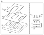
- a transformer 11 as a coil device 20 is formed by a core 21 (see FIG. 2) and a first winding portion 29 and a second winding portion 30 wound around the core 21, respectively. ing.
- the first winding portion 29 and the second winding portion 30 are electrically insulated.
- the first winding portion 29 includes a coil pattern 37 on the metal base substrate 31 and a wiring body 45a on the wiring member 41.
- the second winding portion 30 includes a coil pattern 38 on the metal base substrate 31 , and wiring bodies 45 g and 45 f on the wiring member 41 .
- the coil pattern 37 and the coil pattern 38 are formed with the insulating layer 35 interposed in the metal base body 33 .
- the wiring main body 45 a (first winding portion 29 ) and the wiring main body 45 g (second winding portion 30 ) are formed on the side of the insulating portion 43 facing the coil patterns 37 and 38 .
- the wiring main body 45f (second winding portion 30) is formed on the side opposite to the side facing the coil patterns 37 and 38 in the insulating portion 43. As shown in FIG.
- the wiring main body 45 a and the coil pattern 37 are electrically connected by a joint member 53 .
- the wiring main body 45 f and the wiring main body 45 g are electrically connected by the through-hole conductive portion 47 .
- the wiring main body 45 g and the coil pattern 38 are electrically connected by a joint member 53 . Since the configuration other than this is the same as the configuration of the coil device 20 shown in FIG. 2 and the like, the same members are denoted by the same reference numerals, and the description thereof will not be repeated unless necessary.
- the first winding portion 29 including the coil pattern 37 and the wiring main body 45a becomes the primary winding 11a (or the secondary winding 11b) of the transformer 11, and the coil pattern 38 and the wiring main body
- the second winding portion 30 including 45g and 45f becomes the secondary winding 11b (or the primary winding 11a) of the transformer 11. As shown in FIG.
- first winding portion 29 (coil pattern 37, wiring main body 45a) and the portion of the second winding portion 30 (coil pattern 38, wiring main body 45f, 45g) located in the outer region of the core 21, respectively.
- the heat generated is radiated to the cooling body 39 via the insulating layer 35 and the metal base body 33 .
- first winding portion 29 (coil pattern 37, wiring main body 45a) and the second winding portion 30 (coil pattern 38, wiring main body 45f, 45g) located in the inner region of the core 21, respectively.
- the heat generated in is also radiated to the cooling body 39 via the insulating layer 35 and the metal base body 33 .
- the second winding portion 30 is arranged on the side closer to the metal base main body 33.
- the insulating portion It is preferable to arrange it on the upper surface side of 43 .
- the number of turns of each of the first winding portion 29 and the second winding portion 30 may be two or more, if necessary.
- a wiring member in which two or more printed circuit boards are laminated may be used as the wiring member 41.
- one printed circuit board and another printed circuit board are electrically connected by a bonding member.
- a multi-layer printed circuit board in which wiring bodies (conductive layers) and insulating portions are alternately laminated may be applied.
- Embodiment 3 a coil device including two coil units will be described as still another example of the coil device.
- the coil device 20 is composed of a first coil unit 18a and a second coil unit 18b as the coil unit 18. As shown in FIG. 35 and 36, the coil device 20 is composed of a first coil unit 18a and a second coil unit 18b as the coil unit 18. As shown in FIG. 35 and 36, the coil device 20 is composed of a first coil unit 18a and a second coil unit 18b as the coil unit 18. As shown in FIG.
- the coil device 20 composed of the first coil unit 18a and the coil device 20 composed of the second coil unit 18b are arranged side by side.
- One coil device 20 (first coil unit 18a) and the other coil device 20 (second coil unit 18b) may be electrically connected in series, or may be electrically connected in parallel. good too.
- a heat diffusion member 75 as a first heat diffusion member is arranged in the cooling body 39 in one coil device 20 .
- a heat diffusion member 75 as a second heat diffusion member is arranged in the cooling body 39 in the other coil device 20 .
- a heat pipe or a vapor chamber, for example, can be applied as the heat diffusion member 75 .
- the heat diffusion member 75 may be made of a material having a thermal conductivity of 300 W/m ⁇ K or more, for example.
- the heat diffusion member 75 in one coil device 20 and the heat diffusion member 75 in the other coil device 20 are connected.
- the heat diffusion member 75 is formed continuously from the cooling body 39 of one coil device 20 to the cooling body 39 of the other coil device 20 .
- the dotted line is shown for the thermal diffusion member 75 on the near side.
- the temperature of the coil device 20 rises as the coil or core heats up.
- the core tends to be magnetically saturated.
- the electrical resistivity of the coil tends to increase. Therefore, it is assumed that the electrical characteristics of the coil device 20 change.
- the heat diffusion member 75 is formed continuously from the cooling body 39 of one coil device 20 to the cooling body 39 of the other coil device 20 .
- the difference between the temperature rise of one coil device 20 and the temperature rise of the other coil device 20 can be reduced.
- it is possible to suppress the operation of the coil device 20 from becoming unstable due to an increase in temperature rise difference, and suppress malfunction of the power conversion device 1 including the coil device 20. can.
- the allowable temperature is determined by the coil device with the larger temperature rise. Therefore, a structure for cooling the coil device having a larger temperature rise is required, and it is assumed that the coil device will be enlarged.
- the heat diffusion member 75 reduces the difference between the temperature rise of one coil device 20 and the temperature rise of the other coil device 20, and can equalize the temperature. This suppresses an increase in the size of the coil device due to an increase in temperature rise difference, and contributes to miniaturization of the power conversion device 1 including the coil device 20 .
- the case where the cooling bodies 39 are arranged in each of the one coil device 20 and the other coil device 20 is taken as an example.
- a cooling body 39 that is formed integrally with the entirety of the one coil device 20 and the other coil device 20 may be applied.
- the present disclosure is effectively used for a coil device in which a winding portion is wound around a core.
Landscapes
- Engineering & Computer Science (AREA)
- Power Engineering (AREA)
- Coils Of Transformers For General Uses (AREA)
- Transformer Cooling (AREA)
- Coils Or Transformers For Communication (AREA)
Abstract
Description
実施の形態1では、コイル装置の一例として平滑リアクトルについて説明する。図2および図3に示すように、コイル装置20は、1つのコイルユニット18から構成される。コイル装置20としての平滑リアクトル13は、1つ以上のループ状の磁路を有するコア21と、コア21に巻回された第1巻線部29とによって形成されている。後述するように、第1巻線部29は、金属ベース基板31におけるコイルパターン37と、配線部材41における配線本体45とを備えている。
図7に示すように、スリット27の上方に位置する、配線部材41の配線本体45の部分を覆うように、絶縁部材59を配置してもよい(第1例)。また、図8に示すように、スリット27を覆うように、絶縁部材59を配置してもよい(第2例)。絶縁部材59は、電気的絶縁性を有する材料から形成されていればよい。絶縁部材59として、たとえば、ポリイミドテープにシリコン系粘着剤を塗布した粘着テープを適用してもよい。
図9に示すように、配線部材41としては、絶縁部43において金属ベース基板31と対向する表面(下面)に配線本体45aが形成され、絶縁部43において金属ベース基板31と対向する表面とは反対側の表面(上面)に配線本体45bが形成された配線部材41を適用してもよい。配線本体45aと配線本体45bとは、絶縁部43を貫通するように形成されたスルーホール導電部47によって電気的に接続されている。なお、図9に示すコイル装置20において、図7または図8に示される絶縁部材59を配置してもよい。
図10に示すように、絶縁部43において金属ベース基板31と対向する表面のうち、スリット27の直上に位置する部分を除く態様で、配線本体45aを形成するようにしてもよい。スリット27の直上に位置する絶縁部43の表面の部分に配線本体45aを配置させない構造とすることで、図7または図8に示される絶縁部材59を配置することなく、配線本体45aと金属ベース本体33との距離(空間距離)を確保することができる。
図11に示すように、コア21と金属ベース基板31とを、固定テープ61によって互いに固定するようにしてもよい。固定テープ61として、たとえば、ポリエステルフィルムにアクリル系粘着剤を塗布した粘着テープを適用することができる。冷却体39では、コア21と金属ベース基板31とを固定する固定テープ61が、冷却体39に干渉しないように、溝部40を含む各部の寸法が設定されている。なお、金属ベース基板31は、たとえば、ネジ(図示せず)によって冷却体39に固定される。
ここでは、E型コア23とI型コア25とからなるコア21を適用したコイル装置20において、金属ベース本体(金属ベース基板)に形成されるスリットの配置位置のバリエーションについて説明する。図12に、金属ベース本体33に形成されるスリット27の配置位置として、図4に示される第1の配置例の他に、第2の配置例と第3の配置例とを示す。
ここでは、コア21として2つのU型コアを適用したコイル装置20において、金属ベース本体(金属ベース基板)に形成されるスリットの配置位置のバリエーションについて説明する。図13に、金属ベース本体33に形成されるスリット27の配置位置として、第1の配置例、第2の配置例および第3の配置例を示す。
配線部材41(配線本体45)において発生する熱を抑えるために、コイルパターン37と配線本体45とを電気的に並列に接続させた区間を設けるようにしてもよい。図16および図17に示すように、コア21(図2参照)に巻回される第1巻線部29において、位置P1と位置P2との間の区間、位置P3と位置P4との間の区間および位置P5と位置P6との間の区間のそれぞれでは、電気的に並列に接続された配線本体45とコイルパターン37とが配置されている。
配線部材41として、絶縁部に、配線本体とは電気的に絶縁された導電部が形成された配線部材を適用し、その導電部を金属ベース基板31を介して冷却体39に熱接合させるようにしてもよい。
コイル装置20の小型化の観点からでは、第1巻線部29の巻き数を増やすことでコアの小型化に寄与することができる。図20に示すように、コイル装置20では、配線部材41における配線本体45(配線本体45a、配線本体45b)は、第1巻線部29の一部を構成する。その配線本体45が、E型コア23の脚部23c(図2参照)のまわりに、2回巻回されている(巻き数2(2ターン))。
配線部材として、金属バスバーを適用してもよい。図21および図22に示すように、配線部材41は、配線本体45となる金属バスバー45dと、金属バスバー45dを被覆する絶縁部43aおよび絶縁部43bとを備えている。絶縁部43aは、金属バスバー45dの上面の一部を露出する態様で形成されている。絶縁部43bは、金属バスバー45dの下面の一部を露出する態様で形成されている。
配線本体45として金属バスバー45dを適用する場合、図23に示すように、屈曲した金属バスバー45eを適用してもよい。金属バスバー45eは、スリット27から遠ざかる方向に向かって屈曲(または湾曲)している。これにより、金属バスバー45eと金属ベース本体33との間の距離が伸び、金属バスバー45eと金属ベース本体33との間の領域(空間)において、絶縁破壊が生じるのを効果的に防止することができる。その結果、コイル装置20の電気的絶縁性を向上させることができ、ひいては、電力変換装置1の電気的絶縁性を向上させることができる。
図24に示すように、コア21と金属ベース本体33との間に、それぞれ第2熱伝導部材としての熱伝導部材63aおよび熱伝導部材63bを介在させてもよい。熱伝導部材63aは、E型コア23の脚部23aと脚部23cとの間に位置するE型コア23における面23acと金属ベース本体33の第2主面33bとの間に挟み込まれるように配置されている。熱伝導部材63bは、E型コア23の脚部23cと脚部23bとの間に位置するE型コア23における面23bcと金属ベース本体33の第2主面33bとの間に挟み込まれるように配置されている。
コア21において発生する熱を、冷却体へ放熱する放熱経路を増やす構造としてもよい。図25に示すように、コイル装置20では、コア21は、支柱67と押さえ部材65とによって冷却体39に押さえ付けられている。ここでは、押さえ部材65として、平板状部材65aが適用されている。支柱67は、冷却体39から突出するように形成されている。
また、図26に示すように、平板状部材65aとI型コア25(コア21)との間に、第3熱伝導部材としての熱伝導部材69を介在させてもよい。これにより、コア21において発生する熱を、熱伝導部材69を介して平板状部材65aおよび支柱67へ効率よく伝導させ、その支柱に67に伝導した熱を冷却体39へ放熱することができる。その結果、放熱のためにコア21を大型化する必要性がなくなり、コイル装置20の小型化、ひいては、電力変換装置1の小型化にさらに寄与することができる。
さらに、図27に示すように、コア21に作用する応力を緩和する観点から、押さえ部材65として、板バネ部材65bを適用してもよい。この場合には、板バネ部材65bによってコア21を押さえ付ける際に、板バネ部材65bが変形することで、コア21に作用する応力が緩和される。これにより、コア21の靭性を向上させるために、コア21を大型化する必要性がなく、コイル装置20の小型化、ひいては、電力変換装置1の小型化に寄与することができる。
また、図28に示すように、コア21において発生する熱を、冷却体へ放熱する放熱経路をさらに増やすため、押さえ部材65としてT型部材65cを適用してもよい。T型部材65cは、平板状部材65a(図25参照)に、冷却体39に向かって突出する凸部65ccが形成された構造を有する。
図29に示すように、スリット27を挟んで対向する金属ベース本体33の端面33c間における電気的短絡を防止するために、一方の端面33cと他方の端面33cとのそれぞれに、短絡防止部材71を形成してもよい。短絡防止部材71は、電気的絶縁性を有する部材であればよく、たとえば、ポリイミドフィルムにシリコン系粘着剤を塗布した粘着テープを適用することができる。
図30に示すように、金属ベース基板31および配線部材41を封止部材73によって封止させてもよい。この場合には、冷却体39として、上方に向かって開口した箱型(箱状)の冷却体39が適用される。箱型の冷却体39に収容された金属ベース基板31および配線部材41を封止するように、箱型の冷却体39内に封止部材73が充填される。
実施の形態2では、コイル装置の他の例としてトランスについて説明する。図31に示すように、コイル装置20としてのトランス11は、コア21(図2参照)と、コア21にそれぞれ巻回された第1巻線部29および第2巻線部30とによって形成されている。第1巻線部29と第2巻線部30とは、電気的に絶縁されている。
実施の形態3では、コイル装置のさらに他の例として、2つのコイルユニットを備えたコイル装置について説明する。図35および図36に示すように、コイル装置20は、コイルユニット18として、第1コイルユニット18aと第2コイルユニット18bとから構成されている。
Claims (21)
- 1つ以上のコイルユニットを有するコイル装置であって、
前記コイルユニットは、
1つ以上のループ状の磁路を有するコアと、
前記コアによって取り囲まれた前記コアの内側領域を通り抜ける態様で、前記コアに巻回された第1巻線部と
を備え、
前記コアの前記内側領域と前記コアの外側領域とには、金属ベース本体に絶縁層を介在させてコイルパターンが形成された金属ベース基板が配置され、
前記金属ベース基板には、前記コアが貫通する第1貫通穴が形成され、
前記金属ベース本体に対して、前記絶縁層および前記コイルパターンが形成されている側とは反対側に冷却体が熱接合され、
前記第1巻線部は、前記コイルパターンを含む、コイル装置。 - 前記金属ベース基板は、前記コアを連続的に取り囲まないように分断するスリットが形成される態様で、前記コアの前記内側領域と前記外側領域とから前記コアを取り囲むように配置され、
前記スリットは、前記第1貫通穴に繋がるように形成され、
前記スリットを挟んで、一方に位置する前記金属ベース基板の部分に形成された前記コイルパターンと、他方に位置する前記金属ベース基板の部分に形成された前記コイルパターンとを電気的に接続する、配線本体を含む配線部材が配置され、
前記第1巻線部は、前記配線部材における前記配線本体を含む、請求項1記載のコイル装置。 - 前記スリットは、前記コアの前記内側領域に配置された、請求項2記載のコイル装置。
- 前記配線部材は、絶縁部を含み、
前記配線本体は前記絶縁部に配置された、請求項2または3に記載のコイル装置。 - 前記配線部材は、プリント基板であり、
前記配線本体は、前記プリント基板に配置された、請求項2~4のいずれか1項に記載のコイル装置。 - 前記配線部材における前記配線本体と、前記金属ベース基板に形成された前記コイルパターンとが、接合部材によって電気的に接続された、請求項2~5のいずれか1項に記載のコイル装置。
- 前記金属ベース基板と前記配線部材とが、第1熱伝導部材を介して熱結合している、請求項2~6のいずれか1項に記載のコイル装置。
- 前記スリットに対向する前記配線部材の部分と前記スリットとの間に、絶縁部材が配置された、請求項2~7のいずれか1項に記載のコイル装置。
- 前記スリットを挟んで前記一方に位置する前記金属ベース基板の端面と、前記他方に位置する前記金属ベース基板の端面との間に、短絡防止部材が配置された、請求項2~8のいずれか1項に記載のコイル装置。
- 前記配線部材は、前記金属ベース基板から離れる方向に向かって屈曲した屈曲配線本体を含む、請求項2~9のいずれか1項に記載のコイル装置。
- 前記金属ベース基板および前記配線部材は、封止部材によって封止された、請求項2~10のいずれか1項に記載のコイル装置。
- 前記金属ベース基板に形成された前記第1貫通穴に挿通された前記コアと、前記金属ベース基板との間に、第2熱伝導部材を介在させた、請求項1~11のいずれか1項に記載のコイル装置。
- 前記金属ベース基板における前記金属ベース本体は、互いに対向する第1主面および第2主面を有し、
前記第1主面上に前記コイルパターンが形成され、
前記金属ベース本体の前記第2主面と前記コアとが、前記第2熱伝導部材を介して熱接合された、請求項12記載のコイル装置。 - 前記冷却体に熱接合し、前記冷却体から前記コアが配置されている側に向かって突出するように配置された支柱と、
前記コアを覆うように前記支柱に熱接合する態様で前記支柱に固定され、前記コアを前記冷却体が位置する側へ押さえ付ける押さえ部材と
を備えた、請求項1~13のいずれか1項に記載のコイル装置。 - 前記コアと前記押さえ部材との間に、第3熱伝導部材を介在させた、請求項14記載のコイル装置。
- 前記押さえ部材は、前記コアに向かって付勢する弾性部材を含む、請求項14記載のコイル装置。
- 前記押さえ部材は、前記冷却体に向かって突出し、前記冷却体に熱接合する凸部を備え、
前記コアには、前記凸部が挿通する第2貫通穴が形成された、請求項14記載のコイル装置。 - 前記コアの前記内側領域を通り抜ける態様で前記コアに巻回され、前記第1巻線部と電気的に絶縁された第2巻線部を備えた、請求項1~17のいずれか1項に記載のコイル装置。
- 前記コアの前記内側領域を通り抜ける態様で前記コアに巻回され、前記第1巻線部と電気的に絶縁された第2巻線部を備え、
前記配線部材には、互いに電気的に絶縁された前記第1巻線部と前記第2巻線部とが配置された、請求項2~11のいずれか1項に記載のコイル装置。 - 前記コイルユニットは、
第1コイルユニットと、
第2コイルユニットと
を含み、
前記第1コイルユニットと前記第2コイルユニットとは、互いに隣り合うように配置され、
前記第1コイルユニットにおける前記冷却体には、第1熱拡散部材が配置され、
前記第2コイルユニットにおける前記冷却体には、第2熱拡散部材が配置され、
前記第1熱拡散部材と前記第2熱拡散部材とは互いに繋がるように配置された、請求項1~19のいずれか1項に記載のコイル装置。 - 請求項1~20のいずれか1項に記載のコイル装置を備えた、電力変換装置。
Priority Applications (2)
| Application Number | Priority Date | Filing Date | Title |
|---|---|---|---|
| JP2023525719A JP7580599B2 (ja) | 2021-06-03 | 2022-05-19 | コイル装置および電力変換装置 |
| US18/553,581 US20240177914A1 (en) | 2021-06-03 | 2022-05-19 | Coil device and power conversion device |
Applications Claiming Priority (2)
| Application Number | Priority Date | Filing Date | Title |
|---|---|---|---|
| JP2021-093693 | 2021-06-03 | ||
| JP2021093693 | 2021-06-03 |
Publications (1)
| Publication Number | Publication Date |
|---|---|
| WO2022255115A1 true WO2022255115A1 (ja) | 2022-12-08 |
Family
ID=84323229
Family Applications (1)
| Application Number | Title | Priority Date | Filing Date |
|---|---|---|---|
| PCT/JP2022/020815 Ceased WO2022255115A1 (ja) | 2021-06-03 | 2022-05-19 | コイル装置および電力変換装置 |
Country Status (3)
| Country | Link |
|---|---|
| US (1) | US20240177914A1 (ja) |
| JP (1) | JP7580599B2 (ja) |
| WO (1) | WO2022255115A1 (ja) |
Cited By (3)
| Publication number | Priority date | Publication date | Assignee | Title |
|---|---|---|---|---|
| WO2024116850A1 (ja) * | 2022-11-30 | 2024-06-06 | 三菱電機株式会社 | コイル装置および電力変換装置 |
| JP2024164409A (ja) * | 2023-05-15 | 2024-11-27 | 三菱電機株式会社 | 電力変換装置 |
| JP7854964B2 (ja) | 2023-05-15 | 2026-05-07 | 三菱電機株式会社 | 電力変換装置 |
Citations (4)
| Publication number | Priority date | Publication date | Assignee | Title |
|---|---|---|---|---|
| US20020163818A1 (en) * | 2001-03-05 | 2002-11-07 | Green Mark D. | Magnetic device and method of manufacture therefor |
| JP2013168401A (ja) * | 2012-02-14 | 2013-08-29 | Mitsubishi Electric Corp | 車載用電力変換装置 |
| JP2014093405A (ja) * | 2012-11-02 | 2014-05-19 | Tdk Corp | コイル装置 |
| JP2020161725A (ja) * | 2019-03-27 | 2020-10-01 | 株式会社ダイヘン | トランス |
-
2022
- 2022-05-19 JP JP2023525719A patent/JP7580599B2/ja active Active
- 2022-05-19 WO PCT/JP2022/020815 patent/WO2022255115A1/ja not_active Ceased
- 2022-05-19 US US18/553,581 patent/US20240177914A1/en active Pending
Patent Citations (4)
| Publication number | Priority date | Publication date | Assignee | Title |
|---|---|---|---|---|
| US20020163818A1 (en) * | 2001-03-05 | 2002-11-07 | Green Mark D. | Magnetic device and method of manufacture therefor |
| JP2013168401A (ja) * | 2012-02-14 | 2013-08-29 | Mitsubishi Electric Corp | 車載用電力変換装置 |
| JP2014093405A (ja) * | 2012-11-02 | 2014-05-19 | Tdk Corp | コイル装置 |
| JP2020161725A (ja) * | 2019-03-27 | 2020-10-01 | 株式会社ダイヘン | トランス |
Cited By (3)
| Publication number | Priority date | Publication date | Assignee | Title |
|---|---|---|---|---|
| WO2024116850A1 (ja) * | 2022-11-30 | 2024-06-06 | 三菱電機株式会社 | コイル装置および電力変換装置 |
| JP2024164409A (ja) * | 2023-05-15 | 2024-11-27 | 三菱電機株式会社 | 電力変換装置 |
| JP7854964B2 (ja) | 2023-05-15 | 2026-05-07 | 三菱電機株式会社 | 電力変換装置 |
Also Published As
| Publication number | Publication date |
|---|---|
| US20240177914A1 (en) | 2024-05-30 |
| JP7580599B2 (ja) | 2024-11-11 |
| JPWO2022255115A1 (ja) | 2022-12-08 |
Similar Documents
| Publication | Publication Date | Title |
|---|---|---|
| JP5359749B2 (ja) | トランス及びスイッチング電源装置 | |
| US11206729B2 (en) | Power circuit device | |
| US8188829B2 (en) | Coil substrate structure, substrate holding structure, and switching power supply | |
| US11432437B2 (en) | Power converter | |
| US10916367B2 (en) | Circuit device and power conversion device | |
| US8237535B2 (en) | Integral planar transformer and busbar | |
| JP7171736B2 (ja) | 回路装置及び電力変換装置 | |
| JP7326782B2 (ja) | トランスおよび電源装置 | |
| JP7345621B2 (ja) | 電力変換装置および電力変換装置の製造方法 | |
| CN105144317A (zh) | 磁器件 | |
| JP7062130B2 (ja) | 電力変換装置 | |
| JP7580599B2 (ja) | コイル装置および電力変換装置 | |
| JP2023184134A (ja) | トランス | |
| JP6377279B2 (ja) | 電力変換装置 | |
| JP7814549B2 (ja) | コイル装置および電力変換装置 | |
| JP7660597B2 (ja) | ラミネートコイルの製造方法、並びにラミネートコイル、コイル装置および電力変換装置 | |
| CN115588962A (zh) | 功率转换装置和断路机构 | |
| WO2025079521A1 (ja) | 電力変換システム | |
| WO2025079522A1 (ja) | 電力変換装置 | |
| JP7118285B2 (ja) | ラミネートコイル、コイル装置および電力変換装置 | |
| JPH0748946B2 (ja) | スイッチング電源装置 |
Legal Events
| Date | Code | Title | Description |
|---|---|---|---|
| 121 | Ep: the epo has been informed by wipo that ep was designated in this application |
Ref document number: 22815867 Country of ref document: EP Kind code of ref document: A1 |
|
| WWE | Wipo information: entry into national phase |
Ref document number: 18553581 Country of ref document: US Ref document number: 2023525719 Country of ref document: JP |
|
| NENP | Non-entry into the national phase |
Ref country code: DE |
|
| 122 | Ep: pct application non-entry in european phase |
Ref document number: 22815867 Country of ref document: EP Kind code of ref document: A1 |