WO2022255053A1 - 半導体装置 - Google Patents
半導体装置 Download PDFInfo
- Publication number
- WO2022255053A1 WO2022255053A1 PCT/JP2022/019961 JP2022019961W WO2022255053A1 WO 2022255053 A1 WO2022255053 A1 WO 2022255053A1 JP 2022019961 W JP2022019961 W JP 2022019961W WO 2022255053 A1 WO2022255053 A1 WO 2022255053A1
- Authority
- WO
- WIPO (PCT)
- Prior art keywords
- semiconductor element
- clip
- semiconductor device
- lead frame
- region
- Prior art date
- Legal status (The legal status is an assumption and is not a legal conclusion. Google has not performed a legal analysis and makes no representation as to the accuracy of the status listed.)
- Ceased
Links
Images





Classifications
-
- H—ELECTRICITY
- H10—SEMICONDUCTOR DEVICES; ELECTRIC SOLID-STATE DEVICES NOT OTHERWISE PROVIDED FOR
- H10W—GENERIC PACKAGES, INTERCONNECTIONS, CONNECTORS OR OTHER CONSTRUCTIONAL DETAILS OF DEVICES COVERED BY CLASS H10
- H10W72/00—Interconnections or connectors in packages
- H10W72/90—Bond pads, in general
-
- H—ELECTRICITY
- H10—SEMICONDUCTOR DEVICES; ELECTRIC SOLID-STATE DEVICES NOT OTHERWISE PROVIDED FOR
- H10W—GENERIC PACKAGES, INTERCONNECTIONS, CONNECTORS OR OTHER CONSTRUCTIONAL DETAILS OF DEVICES COVERED BY CLASS H10
- H10W70/00—Package substrates; Interposers; Redistribution layers [RDL]
- H10W70/40—Leadframes
- H10W70/481—Leadframes for devices being provided for in groups H10D8/00 - H10D48/00
-
- H—ELECTRICITY
- H10—SEMICONDUCTOR DEVICES; ELECTRIC SOLID-STATE DEVICES NOT OTHERWISE PROVIDED FOR
- H10W—GENERIC PACKAGES, INTERCONNECTIONS, CONNECTORS OR OTHER CONSTRUCTIONAL DETAILS OF DEVICES COVERED BY CLASS H10
- H10W70/00—Package substrates; Interposers; Redistribution layers [RDL]
- H10W70/40—Leadframes
- H10W70/464—Additional interconnections in combination with leadframes
- H10W70/466—Tape carriers or flat leads
-
- H—ELECTRICITY
- H10—SEMICONDUCTOR DEVICES; ELECTRIC SOLID-STATE DEVICES NOT OTHERWISE PROVIDED FOR
- H10W—GENERIC PACKAGES, INTERCONNECTIONS, CONNECTORS OR OTHER CONSTRUCTIONAL DETAILS OF DEVICES COVERED BY CLASS H10
- H10W72/00—Interconnections or connectors in packages
- H10W72/071—Connecting or disconnecting
- H10W72/073—Connecting or disconnecting of die-attach connectors
-
- H—ELECTRICITY
- H10—SEMICONDUCTOR DEVICES; ELECTRIC SOLID-STATE DEVICES NOT OTHERWISE PROVIDED FOR
- H10W—GENERIC PACKAGES, INTERCONNECTIONS, CONNECTORS OR OTHER CONSTRUCTIONAL DETAILS OF DEVICES COVERED BY CLASS H10
- H10W72/00—Interconnections or connectors in packages
- H10W72/60—Strap connectors, e.g. thick copper clips for grounding of power devices
-
- H—ELECTRICITY
- H10—SEMICONDUCTOR DEVICES; ELECTRIC SOLID-STATE DEVICES NOT OTHERWISE PROVIDED FOR
- H10W—GENERIC PACKAGES, INTERCONNECTIONS, CONNECTORS OR OTHER CONSTRUCTIONAL DETAILS OF DEVICES COVERED BY CLASS H10
- H10W74/00—Encapsulations, e.g. protective coatings
- H10W74/40—Encapsulations, e.g. protective coatings characterised by their materials
-
- H—ELECTRICITY
- H10—SEMICONDUCTOR DEVICES; ELECTRIC SOLID-STATE DEVICES NOT OTHERWISE PROVIDED FOR
- H10W—GENERIC PACKAGES, INTERCONNECTIONS, CONNECTORS OR OTHER CONSTRUCTIONAL DETAILS OF DEVICES COVERED BY CLASS H10
- H10W72/00—Interconnections or connectors in packages
- H10W72/30—Die-attach connectors
-
- H—ELECTRICITY
- H10—SEMICONDUCTOR DEVICES; ELECTRIC SOLID-STATE DEVICES NOT OTHERWISE PROVIDED FOR
- H10W—GENERIC PACKAGES, INTERCONNECTIONS, CONNECTORS OR OTHER CONSTRUCTIONAL DETAILS OF DEVICES COVERED BY CLASS H10
- H10W72/00—Interconnections or connectors in packages
- H10W72/50—Bond wires
-
- H—ELECTRICITY
- H10—SEMICONDUCTOR DEVICES; ELECTRIC SOLID-STATE DEVICES NOT OTHERWISE PROVIDED FOR
- H10W—GENERIC PACKAGES, INTERCONNECTIONS, CONNECTORS OR OTHER CONSTRUCTIONAL DETAILS OF DEVICES COVERED BY CLASS H10
- H10W72/00—Interconnections or connectors in packages
- H10W72/50—Bond wires
- H10W72/541—Dispositions of bond wires
- H10W72/547—Dispositions of multiple bond wires
- H10W72/5473—Dispositions of multiple bond wires multiple bond wires connected to a common bond pad
-
- H—ELECTRICITY
- H10—SEMICONDUCTOR DEVICES; ELECTRIC SOLID-STATE DEVICES NOT OTHERWISE PROVIDED FOR
- H10W—GENERIC PACKAGES, INTERCONNECTIONS, CONNECTORS OR OTHER CONSTRUCTIONAL DETAILS OF DEVICES COVERED BY CLASS H10
- H10W72/00—Interconnections or connectors in packages
- H10W72/50—Bond wires
- H10W72/551—Materials of bond wires
- H10W72/552—Materials of bond wires comprising metals or metalloids, e.g. silver
- H10W72/5522—Materials of bond wires comprising metals or metalloids, e.g. silver comprising gold [Au]
-
- H—ELECTRICITY
- H10—SEMICONDUCTOR DEVICES; ELECTRIC SOLID-STATE DEVICES NOT OTHERWISE PROVIDED FOR
- H10W—GENERIC PACKAGES, INTERCONNECTIONS, CONNECTORS OR OTHER CONSTRUCTIONAL DETAILS OF DEVICES COVERED BY CLASS H10
- H10W72/00—Interconnections or connectors in packages
- H10W72/50—Bond wires
- H10W72/551—Materials of bond wires
- H10W72/552—Materials of bond wires comprising metals or metalloids, e.g. silver
- H10W72/5524—Materials of bond wires comprising metals or metalloids, e.g. silver comprising aluminium [Al]
-
- H—ELECTRICITY
- H10—SEMICONDUCTOR DEVICES; ELECTRIC SOLID-STATE DEVICES NOT OTHERWISE PROVIDED FOR
- H10W—GENERIC PACKAGES, INTERCONNECTIONS, CONNECTORS OR OTHER CONSTRUCTIONAL DETAILS OF DEVICES COVERED BY CLASS H10
- H10W72/00—Interconnections or connectors in packages
- H10W72/60—Strap connectors, e.g. thick copper clips for grounding of power devices
- H10W72/621—Structures or relative sizes of strap connectors
- H10W72/622—Multilayered strap connectors, e.g. having a coating on a lowermost surface of a core
- H10W72/623—Multilayered strap connectors, e.g. having a coating on a lowermost surface of a core characterised by the structures of the outermost layers, e.g. multilayered coatings
-
- H—ELECTRICITY
- H10—SEMICONDUCTOR DEVICES; ELECTRIC SOLID-STATE DEVICES NOT OTHERWISE PROVIDED FOR
- H10W—GENERIC PACKAGES, INTERCONNECTIONS, CONNECTORS OR OTHER CONSTRUCTIONAL DETAILS OF DEVICES COVERED BY CLASS H10
- H10W72/00—Interconnections or connectors in packages
- H10W72/60—Strap connectors, e.g. thick copper clips for grounding of power devices
- H10W72/631—Shapes of strap connectors
- H10W72/634—Cross-sectional shape
-
- H—ELECTRICITY
- H10—SEMICONDUCTOR DEVICES; ELECTRIC SOLID-STATE DEVICES NOT OTHERWISE PROVIDED FOR
- H10W—GENERIC PACKAGES, INTERCONNECTIONS, CONNECTORS OR OTHER CONSTRUCTIONAL DETAILS OF DEVICES COVERED BY CLASS H10
- H10W72/00—Interconnections or connectors in packages
- H10W72/60—Strap connectors, e.g. thick copper clips for grounding of power devices
- H10W72/641—Dispositions of strap connectors
- H10W72/645—Dispositions of strap connectors of outermost layers of multilayered strap connectors, e.g. coating being only on a part of a core
-
- H—ELECTRICITY
- H10—SEMICONDUCTOR DEVICES; ELECTRIC SOLID-STATE DEVICES NOT OTHERWISE PROVIDED FOR
- H10W—GENERIC PACKAGES, INTERCONNECTIONS, CONNECTORS OR OTHER CONSTRUCTIONAL DETAILS OF DEVICES COVERED BY CLASS H10
- H10W72/00—Interconnections or connectors in packages
- H10W72/60—Strap connectors, e.g. thick copper clips for grounding of power devices
- H10W72/651—Materials of strap connectors
- H10W72/652—Materials of strap connectors comprising metals or metalloids, e.g. silver
-
- H—ELECTRICITY
- H10—SEMICONDUCTOR DEVICES; ELECTRIC SOLID-STATE DEVICES NOT OTHERWISE PROVIDED FOR
- H10W—GENERIC PACKAGES, INTERCONNECTIONS, CONNECTORS OR OTHER CONSTRUCTIONAL DETAILS OF DEVICES COVERED BY CLASS H10
- H10W72/00—Interconnections or connectors in packages
- H10W72/60—Strap connectors, e.g. thick copper clips for grounding of power devices
- H10W72/651—Materials of strap connectors
- H10W72/653—Materials of strap connectors not comprising solid metals or solid metalloids, e.g. polymers, ceramics or liquids
-
- H—ELECTRICITY
- H10—SEMICONDUCTOR DEVICES; ELECTRIC SOLID-STATE DEVICES NOT OTHERWISE PROVIDED FOR
- H10W—GENERIC PACKAGES, INTERCONNECTIONS, CONNECTORS OR OTHER CONSTRUCTIONAL DETAILS OF DEVICES COVERED BY CLASS H10
- H10W72/00—Interconnections or connectors in packages
- H10W72/60—Strap connectors, e.g. thick copper clips for grounding of power devices
- H10W72/651—Materials of strap connectors
- H10W72/655—Materials of strap connectors of outermost layers of multilayered strap connectors, e.g. material of a coating
-
- H—ELECTRICITY
- H10—SEMICONDUCTOR DEVICES; ELECTRIC SOLID-STATE DEVICES NOT OTHERWISE PROVIDED FOR
- H10W—GENERIC PACKAGES, INTERCONNECTIONS, CONNECTORS OR OTHER CONSTRUCTIONAL DETAILS OF DEVICES COVERED BY CLASS H10
- H10W72/00—Interconnections or connectors in packages
- H10W72/851—Dispositions of multiple connectors or interconnections
-
- H—ELECTRICITY
- H10—SEMICONDUCTOR DEVICES; ELECTRIC SOLID-STATE DEVICES NOT OTHERWISE PROVIDED FOR
- H10W—GENERIC PACKAGES, INTERCONNECTIONS, CONNECTORS OR OTHER CONSTRUCTIONAL DETAILS OF DEVICES COVERED BY CLASS H10
- H10W72/00—Interconnections or connectors in packages
- H10W72/851—Dispositions of multiple connectors or interconnections
- H10W72/853—On the same surface
- H10W72/871—Bond wires and strap connectors
-
- H—ELECTRICITY
- H10—SEMICONDUCTOR DEVICES; ELECTRIC SOLID-STATE DEVICES NOT OTHERWISE PROVIDED FOR
- H10W—GENERIC PACKAGES, INTERCONNECTIONS, CONNECTORS OR OTHER CONSTRUCTIONAL DETAILS OF DEVICES COVERED BY CLASS H10
- H10W72/00—Interconnections or connectors in packages
- H10W72/851—Dispositions of multiple connectors or interconnections
- H10W72/874—On different surfaces
- H10W72/884—Die-attach connectors and bond wires
-
- H—ELECTRICITY
- H10—SEMICONDUCTOR DEVICES; ELECTRIC SOLID-STATE DEVICES NOT OTHERWISE PROVIDED FOR
- H10W—GENERIC PACKAGES, INTERCONNECTIONS, CONNECTORS OR OTHER CONSTRUCTIONAL DETAILS OF DEVICES COVERED BY CLASS H10
- H10W72/00—Interconnections or connectors in packages
- H10W72/851—Dispositions of multiple connectors or interconnections
- H10W72/874—On different surfaces
- H10W72/886—Die-attach connectors and strap connectors
-
- H—ELECTRICITY
- H10—SEMICONDUCTOR DEVICES; ELECTRIC SOLID-STATE DEVICES NOT OTHERWISE PROVIDED FOR
- H10W—GENERIC PACKAGES, INTERCONNECTIONS, CONNECTORS OR OTHER CONSTRUCTIONAL DETAILS OF DEVICES COVERED BY CLASS H10
- H10W72/00—Interconnections or connectors in packages
- H10W72/90—Bond pads, in general
- H10W72/921—Structures or relative sizes of bond pads
- H10W72/926—Multiple bond pads having different sizes
-
- H—ELECTRICITY
- H10—SEMICONDUCTOR DEVICES; ELECTRIC SOLID-STATE DEVICES NOT OTHERWISE PROVIDED FOR
- H10W—GENERIC PACKAGES, INTERCONNECTIONS, CONNECTORS OR OTHER CONSTRUCTIONAL DETAILS OF DEVICES COVERED BY CLASS H10
- H10W72/00—Interconnections or connectors in packages
- H10W72/90—Bond pads, in general
- H10W72/931—Shapes of bond pads
- H10W72/932—Plan-view shape, i.e. in top view
-
- H—ELECTRICITY
- H10—SEMICONDUCTOR DEVICES; ELECTRIC SOLID-STATE DEVICES NOT OTHERWISE PROVIDED FOR
- H10W—GENERIC PACKAGES, INTERCONNECTIONS, CONNECTORS OR OTHER CONSTRUCTIONAL DETAILS OF DEVICES COVERED BY CLASS H10
- H10W72/00—Interconnections or connectors in packages
- H10W72/90—Bond pads, in general
- H10W72/941—Dispositions of bond pads
- H10W72/944—Dispositions of multiple bond pads
-
- H—ELECTRICITY
- H10—SEMICONDUCTOR DEVICES; ELECTRIC SOLID-STATE DEVICES NOT OTHERWISE PROVIDED FOR
- H10W—GENERIC PACKAGES, INTERCONNECTIONS, CONNECTORS OR OTHER CONSTRUCTIONAL DETAILS OF DEVICES COVERED BY CLASS H10
- H10W72/00—Interconnections or connectors in packages
- H10W72/90—Bond pads, in general
- H10W72/941—Dispositions of bond pads
- H10W72/944—Dispositions of multiple bond pads
- H10W72/9445—Top-view layouts, e.g. mirror arrays
-
- H—ELECTRICITY
- H10—SEMICONDUCTOR DEVICES; ELECTRIC SOLID-STATE DEVICES NOT OTHERWISE PROVIDED FOR
- H10W—GENERIC PACKAGES, INTERCONNECTIONS, CONNECTORS OR OTHER CONSTRUCTIONAL DETAILS OF DEVICES COVERED BY CLASS H10
- H10W72/00—Interconnections or connectors in packages
- H10W72/90—Bond pads, in general
- H10W72/981—Auxiliary members, e.g. spacers
-
- H—ELECTRICITY
- H10—SEMICONDUCTOR DEVICES; ELECTRIC SOLID-STATE DEVICES NOT OTHERWISE PROVIDED FOR
- H10W—GENERIC PACKAGES, INTERCONNECTIONS, CONNECTORS OR OTHER CONSTRUCTIONAL DETAILS OF DEVICES COVERED BY CLASS H10
- H10W90/00—Package configurations
-
- H—ELECTRICITY
- H10—SEMICONDUCTOR DEVICES; ELECTRIC SOLID-STATE DEVICES NOT OTHERWISE PROVIDED FOR
- H10W—GENERIC PACKAGES, INTERCONNECTIONS, CONNECTORS OR OTHER CONSTRUCTIONAL DETAILS OF DEVICES COVERED BY CLASS H10
- H10W90/00—Package configurations
- H10W90/701—Package configurations characterised by the relative positions of pads or connectors relative to package parts
- H10W90/731—Package configurations characterised by the relative positions of pads or connectors relative to package parts of die-attach connectors
- H10W90/736—Package configurations characterised by the relative positions of pads or connectors relative to package parts of die-attach connectors between a chip and a stacked lead frame, conducting package substrate or heat sink
-
- H—ELECTRICITY
- H10—SEMICONDUCTOR DEVICES; ELECTRIC SOLID-STATE DEVICES NOT OTHERWISE PROVIDED FOR
- H10W—GENERIC PACKAGES, INTERCONNECTIONS, CONNECTORS OR OTHER CONSTRUCTIONAL DETAILS OF DEVICES COVERED BY CLASS H10
- H10W90/00—Package configurations
- H10W90/701—Package configurations characterised by the relative positions of pads or connectors relative to package parts
- H10W90/751—Package configurations characterised by the relative positions of pads or connectors relative to package parts of bond wires
- H10W90/753—Package configurations characterised by the relative positions of pads or connectors relative to package parts of bond wires between laterally-adjacent chips
-
- H—ELECTRICITY
- H10—SEMICONDUCTOR DEVICES; ELECTRIC SOLID-STATE DEVICES NOT OTHERWISE PROVIDED FOR
- H10W—GENERIC PACKAGES, INTERCONNECTIONS, CONNECTORS OR OTHER CONSTRUCTIONAL DETAILS OF DEVICES COVERED BY CLASS H10
- H10W90/00—Package configurations
- H10W90/701—Package configurations characterised by the relative positions of pads or connectors relative to package parts
- H10W90/751—Package configurations characterised by the relative positions of pads or connectors relative to package parts of bond wires
- H10W90/756—Package configurations characterised by the relative positions of pads or connectors relative to package parts of bond wires between a chip and a stacked lead frame, conducting package substrate or heat sink
-
- H—ELECTRICITY
- H10—SEMICONDUCTOR DEVICES; ELECTRIC SOLID-STATE DEVICES NOT OTHERWISE PROVIDED FOR
- H10W—GENERIC PACKAGES, INTERCONNECTIONS, CONNECTORS OR OTHER CONSTRUCTIONAL DETAILS OF DEVICES COVERED BY CLASS H10
- H10W90/00—Package configurations
- H10W90/701—Package configurations characterised by the relative positions of pads or connectors relative to package parts
- H10W90/761—Package configurations characterised by the relative positions of pads or connectors relative to package parts of strap connectors
- H10W90/766—Package configurations characterised by the relative positions of pads or connectors relative to package parts of strap connectors between a chip and a stacked lead frame, conducting package substrate or heat sink
-
- H—ELECTRICITY
- H10—SEMICONDUCTOR DEVICES; ELECTRIC SOLID-STATE DEVICES NOT OTHERWISE PROVIDED FOR
- H10W—GENERIC PACKAGES, INTERCONNECTIONS, CONNECTORS OR OTHER CONSTRUCTIONAL DETAILS OF DEVICES COVERED BY CLASS H10
- H10W90/00—Package configurations
- H10W90/811—Multiple chips on leadframes
Definitions
- the present disclosure relates to a semiconductor device in which a clip is joined to a semiconductor element.
- a semiconductor device described in Patent Document 1 includes a die pad, a plurality of leads, a semiconductor element, a clip, a bonding material, and a sealing resin.
- This semiconductor device has a structure in which a clip is joined to an electrode of a semiconductor element and some leads through a joining material, and the semiconductor element and some leads are electrically connected.
- the area of the junction between the semiconductor element and the clip is made as large as possible to reduce the thermal resistance at these junctions, thereby improving the heat dissipation of the semiconductor element.
- the present disclosure relates to a semiconductor device in which a clip is bonded to a semiconductor element, local heat generation in the vicinity of the bonding portion between the semiconductor element and the clip is suppressed, and reliability is improved.
- a semiconductor device comprises a lead frame, a semiconductor element mounted on the lead frame, and an electrode on the surface of the semiconductor element opposite to the lead frame.
- a clip that is bonded via a bonding material, a sealing material that covers the semiconductor element and the clip, and a region between the semiconductor element and the clip that is bonded via the bonding material as a bonding region and a thermal resistance portion disposed in the junction region, the thermal resistance portion having a higher thermal resistance than a region of the junction region different from the thermal resistance portion.
- a thermal resistance portion is arranged in a bonding region bonded via a bonding material between a semiconductor element and a clip, and the thermal resistance portion has a higher thermal resistance than other portions in the bonding region. It has a large configuration. As a result, the portion of the bonding region where the thermal resistance portion is arranged has less heat dissipation than the other portions, so that the amount of heat generated is relatively large. As a result, regions with low heat dissipation are dispersed, and local heat concentration between the clip with high heat dissipation and the region with low heat dissipation in the vicinity of the clip in the semiconductor device is suppressed. Therefore, this semiconductor device is intentionally provided with a region with low heat dissipation, thereby suppressing excessive heat concentration in the vicinity of the connection portion between the semiconductor element and the clip, and current concentration and breakage resulting therefrom. , reliability is improved.
- a semiconductor device comprises a lead frame, a semiconductor element mounted on the lead frame, and electrodes on a surface of the semiconductor element opposite to the lead frame. and a sealing material covering the semiconductor element and the clip, wherein the clips are arranged with a gap from each other and are bonded to the semiconductor element via the bonding material. At least two joints among the plurality of joints are arranged parallel to each other in the same extending direction, and are connected to a region of the electrode including the vicinity of the outer shell.
- This semiconductor device has a configuration in which a semiconductor element and a clip are bonded together, and the clip has a plurality of bonding portions where the clip is bonded to the semiconductor element via a bonding material, and the plurality of bonding portions are arranged apart from each other. It's becoming As a result, the clip having a high heat dissipation is not connected to the portion of the electrode of the semiconductor element located between the plurality of joint portions of the clip, so that the heat dissipation property is lower than that of the joint portion.
- this semiconductor device is intentionally provided with a region with low heat dissipation, thereby suppressing local heat concentration in the vicinity of the connection portion between the semiconductor element and the clip, and current concentration and breakage resulting therefrom. , reliability is improved.
- this semiconductor device has a structure in which the area of the portion of the electrode of the semiconductor element with low heat dissipation on the outer side of the junction is reduced, and the region with low heat dissipation does not occur more than necessary.
- a semiconductor device comprises a lead frame, a semiconductor element mounted on the lead frame, and a surface of the semiconductor element that is bonded to the surface opposite to the lead frame.
- a plurality of clips connected via a material and a sealing material covering the semiconductor element and the clips are provided, and the plurality of clips are arranged with a gap therebetween.
- This semiconductor device has a configuration in which a plurality of different clips are bonded to one semiconductor element via a bonding material, and the plurality of clips are arranged apart from each other. As a result, the portion of the surface of the semiconductor element located between the plurality of clips becomes a region with lower heat dissipation than other portions. As with the other semiconductor devices described above, this disperses areas with low heat dissipation, suppresses local heat concentration in the vicinity of the clip, and the resulting current concentration and damage, thereby improving reliability. An improved effect is obtained.
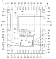
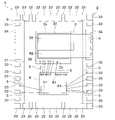
- FIG. 1 is a top layout diagram showing the semiconductor device of the first embodiment
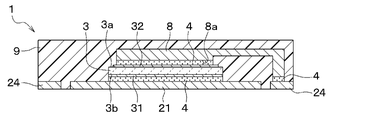
- FIG. FIG. 2 is a cross-sectional view showing a cross section between II-II in FIG. 1
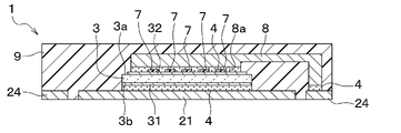
- FIG. 2 is a cross-sectional view showing a cross section between III-III in FIG. 1
- FIG. 3 is a cross-sectional view showing a semiconductor device of a comparative example, which corresponds to FIG. 2
- It is an explanatory view for explaining local heat concentration in a semiconductor device of a comparative example.
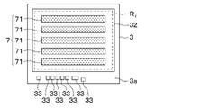
- FIG. 10 is a diagram showing a first arrangement example of an insulating layer as a thermal resistance section between a semiconductor element and a clip
- FIG. 10 is a diagram showing a second arrangement example of insulating layers as a thermal resistance section
- FIG. 10 is a diagram showing a third arrangement example of insulating layers as a thermal resistance section
- FIG. 11 is a diagram showing a fourth arrangement example of insulating layers as a thermal resistance section
- FIG. 11 is a diagram showing a fifth arrangement example of insulating layers as a thermal resistance section
- FIG. 11 is a diagram showing a sixth arrangement example of insulating layers as a thermal resistance section
- It is a figure which shows the example which arrange
- FIG. 3 is a cross-sectional view showing a semiconductor device according to a second embodiment, which corresponds to FIG. 2
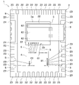
- FIG. 11 is a top layout diagram showing a semiconductor device according to a third embodiment
- FIG. 11 is a top layout diagram showing a modification of the semiconductor device of the third embodiment
- FIG. 11 is a top layout diagram showing a semiconductor device according to a fourth embodiment;
- a semiconductor device 1 according to the first embodiment will be described.
- the semiconductor device 1 of the present embodiment is preferably applied to vehicle-mounted applications such as automobiles, but of course, it can also be applied to other applications.
- FIG. 1 in order to make it easier to understand each member and the arrangement relationship that constitute the semiconductor device 1, a part of the outline of each member covered with a sealing material 9 described later is indicated by a solid line, and members other than the sealing material 9 are indicated by solid lines.
- the outline of the part covered with is indicated by a dashed line.
- the semiconductor device 1 of this embodiment includes, for example, as shown in FIG. and a sealing material 9 . 2 and 3, the semiconductor device 1 includes a bonding material 4 used for connecting the semiconductor element 3 and the clip 8, and an insulating layer 7 disposed between the semiconductor element 3 and the clip 8. , further comprising:
- the lead frame 2 has, for example, a die pad 21, a plurality of first leads 22 extending from the die pad 21, a second lead 23 independent from the die pad 21, and a third lead 24.
- the lead frame 2 is made of, for example, an arbitrary metal material such as Cu (copper) or Fe (iron), an alloy material thereof, or the like.
- the die pad 21 and the plurality of leads 23 and 24 are connected by tie bars (not shown) until the semiconductor device 1 is manufactured. and these are separated.
- a semiconductor element 3 and a control IC 6 for driving control thereof are mounted via a bonding material 4.
- the surface of the die pad 21 opposite to the mounting surface on which the semiconductor element 3 is mounted is exposed from the sealing material 9, for example.
- the plurality of first leads 22 are, for example, arranged in parallel with each other at a distance, and extend outward from the die pad 21 .
- the end surfaces of the plurality of first leads 22 on the side opposite to the die pad 21 side are exposed from the sealing material 9 . This is the same for the second lead 23 and the third lead 24 as well.
- the second lead 23 is independent from the die pad 21 and the third lead 24 and, for example, arranged apart from each other in parallel. Some of the second leads 23 among the plurality of second leads 23 are electrically connected to the control IC 6 via, for example, wires 5 and used to drive the control IC 6 .
- the third lead 24 has a larger planar size than the second lead 23 and is joined to the clip 8 via the joining material 4 .
- the third lead 24 is electrically connected to the second electrode 32 of the semiconductor element 3 via the clip 8 and serves as a current path when the semiconductor element 3 is driven.
- the configuration of the lead frame 2 described above is merely an example, and the number, size, arrangement, etc., of the die pad 21 and the leads 22 to 24 may vary depending on the number, size, etc., of the semiconductor elements 3 and control ICs 6 to be mounted. may be changed as appropriate.
- the lead frame 2 may be partially or wholly plated with Au (gold), Sn (tin), or the like, not shown, for example.
- the semiconductor element 3 is, for example, a vertical power element such as a MOSFET (Metal Oxide Semiconductor Field Effect Transistor) or an IGBT (Insulated Gate Bipolar Transistor).
- the semiconductor element 3 is, for example, mainly made of a semiconductor material such as Si (silicon) or SiC (silicon carbide) in a rectangular plate shape, and is manufactured by a known semiconductor process.
- the semiconductor element 3 has, for example, a surface 3a opposite to the lead frame 2 and a back surface 3b facing the lead frame 2. Electrodes are formed on the front surface 3a and the back surface 3b.
- the semiconductor element 3 has, for example, a first electrode 31 formed on the rear surface 3b, and a second electrode 32 paired with the first electrode 31 and a plurality of third electrodes 33 formed on the front surface 3a.
- the semiconductor element 3 has, for example, a structure in which the first electrode 31 functions as a drain electrode, the second electrode 32 functions as a source electrode, and the third electrode 33 functions as a gate electrode.
- the semiconductor element 3 has a first electrode 31 bonded to the die pad 21 via the bonding material 4 and a second electrode 32 bonded to the clip 8 via the bonding material 4 .
- the third electrode 33 of the semiconductor element 3 is electrically connected to the control IC 6 via the wire 5 , and the current between the first electrode 31 and the second electrode 32 is on/off controlled by the control IC 6 .
- the bonding material 4 is, for example, a conductive bonding material such as solder, and is composed of any bonding material.
- the wire 5 is made of a metal material such as Au (gold) or Al (aluminum), and is connected to the lead frame 2, the semiconductor element 3 and the control IC 6 by wire bonding.
- the control IC 6 is a control element having a control circuit used for current control of the semiconductor element 3, and is, for example, an arbitrary power supply control element corresponding to a power element such as a MOSFET.
- the control IC 6 has, for example, a plurality of electrode pads 61 on one surface, and is connected to the third electrodes 33 of the semiconductor element 3 and the plurality of leads 23 via the wires 5, and is connected to the semiconductor element 3, an external power source, and the like. Electrical communication is possible.
- the control IC 6 is, for example, mounted on the die pad 21 with the bonding material 4 interposed therebetween, similarly to the semiconductor element 3 .
- the insulating layer 7 is disposed between the second electrode 32 of the semiconductor element 3 and the clip 8, for example, as shown in FIG. It is a member that functions as a heat resistance portion that is intentionally increased.
- the insulating layer 7 is made of any insulating material such as PIQ (Polyimide-isoindoloquinazolinedione) or a resist material, and is formed by coating using a dispenser or the like.
- PIQ Polyimide-isoindoloquinazolinedione
- the insulating layer 7 intentionally forms a region with low heat dissipation between the second electrode 32 and the clip 8, and by dispersing the region with low heat dissipation, local heat concentration can be prevented in the region near the clip 8. play a role in preventing Details of this will be described later.
- the clip 8 is a wiring member that is made of, for example, a highly conductive and thermally conductive metal material such as Cu or an alloy material thereof, and that electrically connects the semiconductor element 3 and the third lead 24 .
- One end of the clip 8 is joined to the second electrode 32 of the semiconductor element 3 and the other end is joined to the third lead 24 by the joining material 4 .
- the clip 8 is configured such that the thickness of the portion bonded to the semiconductor element 3 is greater than the thickness of the other portions.
- the clip 8 is obtained by, for example, preparing a plate material made of Cu or the like, forming a partially thin portion by cutting or half-etching, and then bending the plate material.
- the clip 8 is not limited to the structure described above, and may have a structure having a uniform thickness. In this case, the clip 8 is obtained by bending a plate material made of Cu or the like.
- the encapsulant 9 is a member that is made of an arbitrary insulating and hardening resin material such as epoxy resin, and that covers a part of the lead frame 2 and other constituent members of the semiconductor device 1 .
- the encapsulant 9 is molded by any resin molding method such as compression molding using a mold (not shown).
- the above is the basic configuration of the semiconductor device 1 of this embodiment.
- the semiconductor device 100 of the comparative example has a basic configuration similar to that of the semiconductor device 1, but does not have the insulating layer 7 and does not have the insulating layer 7 between the semiconductor element 3 and the clip 8, as shown in FIG. , the insulating layer 7 is not arranged.
- the clip 8 is joined to the second electrode 32 of the semiconductor element 3 , and the joining area between them is approximately the same as the plane area of the second electrode 32 .
- the resistance at the joint portion between the second electrode 32 of the semiconductor element 3 and the clip 8 is reduced, and the amount of heat generated due to the connection resistance at the joint portion is reduced.
- the semiconductor device 100 of the comparative example includes, for example, as shown in FIG. It has a neighboring portion 3ab which is a non-bonded portion.
- a portion 3aa immediately below where the clip 8 made of Cu or the like having high thermal conductivity is arranged serves as a high heat dissipation region RH .
- the vicinity portion 3ab where the sealing material 9 having a lower thermal conductivity than the clip 8 is arranged serves as a low heat radiation region RL .
- the insulating layer 7 is arranged as a thermal resistance portion in the junction region Rj .
- the insulating layer 7 can be composed of, for example, a plurality of island portions 71 arranged in an island shape with a distance therebetween.
- Each of the plurality of island portions 71 has, for example, a substantially rectangular shape when viewed from above, and is arranged inside the outer contour of the joint region Rj , so that the heat resistance in the inner region of the clip 8 is greater than the outer contour. play a role in That is, the portion of the joint surface 8a of the clip 8 located above the island portion 71 has a lower heat dissipation than the other portions of the joint surface 8a.
- the heat generation areas on the joint surface 8a of the clip 8 are dispersed by the number of the island parts 71, the heat concentration in the vicinity of the clip 8 is alleviated, and the resulting current concentration and breakage are suppressed.
- the insulating layer 7 is not limited to the example shown in FIG. 6A, and for example, as shown in FIG. may be aligned and arranged in parallel in the vertical direction of the paper surface. As shown in FIGS. 6C and 6D, the insulating layer 7 may have a configuration in which a plurality of island portions 71 are arranged in parallel with their longitudinal directions aligned in the lateral direction of the paper surface. For example, as shown in FIG. 6E, the insulating layer 7 has a substantially rectangular shape when viewed from the top, and is positioned at a distance from the outline of the bonding region Rj , that is, in a predetermined region including the center of the bonding region Rj . Only one may be arranged. Also, the insulating layer 7 may be substantially circular in top view, as shown in FIG. 6F, for example.
- the insulating layer 7 is arranged at a position away from the vicinity of the outer contour of the joint region Rj , and it is sufficient that the heat generating region in the clip 8 can be dispersed. may be changed as appropriate. From the viewpoint of dispersing heat generation areas in the clip 8 , it is preferable that the insulating layer 7 has a configuration having a plurality of island portions 71 .
- the insulating layer 7 may be arranged between the second electrode 32 and the joint surface 8a of the clip 8. For example, as shown in FIG. good.
- the insulating layer 7 is pattern-formed in advance on the bonding surface 8 a of the clip 8 , for example, before bonding the clip 8 to the semiconductor element 3 .
- the insulating layer 7 may have a plurality of island portions 71 arranged on the bonding surface 8a, or may have a configuration in which only one island portion 71 is arranged on the bonding surface 8a, and is formed on the semiconductor element 3 side. As in the case, the arrangement, configuration, and the like may be changed as appropriate.
- the insulating layer 7 is arranged between the semiconductor element 3 and the clip 8, so that the joint surface 8a of the clip 8 intentionally has a thermal resistance portion with low heat dissipation. It becomes the device 1.
- the heat generated in the junction region Rj between the semiconductor element 3 and the clip 8 is dispersed, and heat concentration, current concentration, and damage caused by the heat concentration in the vicinity portion 3ab of the semiconductor element 3 located in the vicinity of the outer periphery of the clip 8 are prevented. is suppressed, and the effect of improving reliability is obtained.
- the semiconductor device 1 of the present embodiment differs from the first embodiment in that it does not have the insulating layer 7 and the bonding surface 8a of the clip 8 has an uneven shape, as shown in FIG. In this embodiment, this difference will be mainly described.
- the clip 8 has, for example, a plurality of recesses 81 recessed toward the side opposite to the semiconductor element 3 on the bonding surface 8a.
- the bonding surface 8 a of the clip 8 is bonded to the second electrode 32 of the semiconductor element 3 via the bonding material 4 , and the recess 81 is filled with the bonding material 4 .
- the clip 8 functions as a thermal resistance portion having a larger thermal resistance than the other portions because the recessed portion 81 is positioned further away from the semiconductor element 3 than the other portions of the joint surface 8a.
- the clip 8 is in substantially the same state as when the insulating layer 7 is arranged, because the concave portion 81 has less heat dissipation than the other portions of the joint surface 8a and generates more heat. Therefore, the semiconductor device 1 of the present embodiment has a configuration in which the heat generating region is dispersed on the bonding surface 8a of the clip 8, and local heat concentration in the vicinity portion 3ab of the semiconductor element 3 is suppressed.
- concave portion 81 Only one concave portion 81 may be provided on the joint surface 8a, or a plurality of concave portions 81 may be provided and arranged apart from each other. Further, the concave portion 81 is, for example, a rectangular groove and has a depth of about 10 ⁇ m, but is not limited to this, and the depth, shape, dimensions, and the like may be changed as appropriate.
- the semiconductor device 1 can obtain the same effects as those of the first embodiment.
- the semiconductor device 1 does not require the insulating layer 7, there is no influence of aged deterioration of the insulating layer 7, and an effect of further improving reliability can be obtained.
- the semiconductor device 1 of the present embodiment has a structure having a plurality of bonding portions 82 where the clip 8 is bonded to the semiconductor element 3 and does not have the insulating layer 7, as shown in FIG. Differs from one embodiment. In this embodiment, this difference will be mainly described.
- the clip 8 has two joints 82 arranged parallel to each other with a gap therebetween.
- the clip 8 is obtained, for example, by providing a plate material made of Cu or the like with portions having different thicknesses by processing such as cutting or half-etching, and then performing press punching to remove unnecessary portions.
- the two joints 82 are, for example, rectangular when viewed from above, and are arranged in parallel with their extension directions (that is, longitudinal directions) aligned.
- the two bonding portions 82 are arranged, for example, along two opposing sides of a plurality of sides forming the outline of the second electrode 32 of the semiconductor element 3, and are bonded to a predetermined region including the vicinity of the two sides. It is As a result, the area of the second electrode 32 between the joint portion 82 and one side of the outer shell adjacent thereto is reduced, thereby suppressing the spread resistance in the region, and the clip 8 of the second electrode 32 is reduced. The amount of heat generated in the outer shell portion located in the vicinity of is reduced.
- the portion sandwiched between the two joint portions 82 of the clip 8 is in a state where the second electrode 32 of the semiconductor element 3 is exposed, and the sealing material 9 having a lower thermal conductivity than the clip 8 is arranged. Therefore, the area between the two joints 82 of the second electrode 32 has less heat dissipation than the area where the joints 82 are joined, and as a result of the heat-generating areas in the semiconductor element 3 dispersing, the neighboring part 3ab play a role in suppressing the local heat concentration of
- the semiconductor device 1 can obtain the same effects as those of the first embodiment. Moreover, since the insulating layer 7 is not provided, the semiconductor device 1 of the present embodiment can obtain the same effects as those of the second embodiment.
- the semiconductor device 1 of the third embodiment may have a configuration in which the clip 8 has three joint portions 82 arranged apart from each other.
- the gaps between the joints 82 are designed to have heat dissipation properties that are intentionally smaller than those of the joints 82 . It functions as a resistor. Therefore, the semiconductor device 1 uses a clip 8 having a plurality of joints 82 arranged apart from each other, thereby suppressing local heat concentration at the boundary between the second electrode 32 of the semiconductor element 3 and the clip 8. and improve reliability.
- the clip 8 is not limited to the example in which the two or three joints 82 are spaced apart from each other and arranged in parallel as described above, and may have four or more joints 82. . At least two joint portions 82 of the plurality of joint portions 82 of the clip 8 are arranged along two opposing sides among the sides forming the outline of the second electrode 32 of the semiconductor element 3, and the vicinity of the two sides is arranged. It is preferably joined to the containing region.
- the term “nearby” as used herein means, for example, but not limited to, a portion positioned within 1 mm from the side forming the outline of the second electrode 32 .
- the number, arrangement, dimensions, etc. of the joint portions 82 of the clip 8 may be appropriately changed according to the electrodes of the semiconductor element 3 to be joined.
- the semiconductor device 1 can obtain the same effects as those of the third embodiment.
- the semiconductor element 3 has two second electrodes 32 on the surface 3a, and different clips 8 are joined to the two second electrodes 32. , and that the insulating layer 7 is not provided. In this embodiment, this difference will be mainly described.
- the semiconductor element 3 has two second electrodes 32 spaced apart from each other on the surface 3a in this embodiment.
- two second electrodes 32 are paired with a first electrode 31 on the back surface 3b, and voltage application to the third electrode 33 causes current to flow in the thickness direction, that is, in the vertical direction. .
- the number of clips 8 is the same as the number of the second electrodes 32 of the semiconductor element 3, and they are joined to the different second electrodes 32 via the joining material 4.
- the two clips 8 are joined to one semiconductor element 3 , are independent of each other, and are arranged so as not to contact the other clip 8 .
- the region between the two second electrodes 32 of the semiconductor element 3 has less heat dissipation than the region joined to the clip 8, and the heat generating portions are dispersed, so that the clip Local heat concentration in the portion located in the vicinity of 8 is suppressed.
- the semiconductor device 1 can obtain the same effects as those of the first embodiment. Moreover, since the insulating layer 7 is not provided, the semiconductor device 1 of the present embodiment can obtain the same effects as those of the second embodiment.
- the configuration in which one semiconductor element 3 and one control IC 6 are mounted on one die pad 21 has been described as a representative example, but the configuration of the semiconductor device 1 is not limited to this. do not have.
- the semiconductor device 1 may have a plurality of independent die pads 21 and the semiconductor element 3 and the control IC 6 may be mounted on different die pads 21 .
- the semiconductor device 1 may have a configuration in which the control IC 6 is not included in the sealing material 9 and the semiconductor element 3 is connected to the control IC 6 arranged outside.
- the semiconductor device 1 may have, for example, a configuration in which two semiconductor elements 3 are arranged in the sealing material 9, that is, a so-called 2-in-1 configuration, or three or more semiconductor elements 3 may be arranged in the sealing material 9. It may be a configuration that is In this case, the configuration of the lead frame 2, the number of clips 8, and the like are appropriately changed according to the number of semiconductor elements 3, and the like.
Landscapes
- Lead Frames For Integrated Circuits (AREA)
- Cooling Or The Like Of Semiconductors Or Solid State Devices (AREA)
Priority Applications (1)
| Application Number | Priority Date | Filing Date | Title |
|---|---|---|---|
| US18/497,089 US20240063150A1 (en) | 2021-06-04 | 2023-10-30 | Semiconductor device |
Applications Claiming Priority (2)
| Application Number | Priority Date | Filing Date | Title |
|---|---|---|---|
| JP2021094415A JP7694167B2 (ja) | 2021-06-04 | 2021-06-04 | 半導体装置 |
| JP2021-094415 | 2021-06-04 |
Related Child Applications (1)
| Application Number | Title | Priority Date | Filing Date |
|---|---|---|---|
| US18/497,089 Continuation US20240063150A1 (en) | 2021-06-04 | 2023-10-30 | Semiconductor device |
Publications (1)
| Publication Number | Publication Date |
|---|---|
| WO2022255053A1 true WO2022255053A1 (ja) | 2022-12-08 |
Family
ID=84324336
Family Applications (1)
| Application Number | Title | Priority Date | Filing Date |
|---|---|---|---|
| PCT/JP2022/019961 Ceased WO2022255053A1 (ja) | 2021-06-04 | 2022-05-11 | 半導体装置 |
Country Status (3)
| Country | Link |
|---|---|
| US (1) | US20240063150A1 (https=) |
| JP (1) | JP7694167B2 (https=) |
| WO (1) | WO2022255053A1 (https=) |
Citations (5)
| Publication number | Priority date | Publication date | Assignee | Title |
|---|---|---|---|---|
| JP2004047800A (ja) * | 2002-07-12 | 2004-02-12 | Toyota Industries Corp | 接続部材及び接続構造 |
| JP2012069640A (ja) * | 2010-09-22 | 2012-04-05 | Toshiba Corp | 半導体装置及び電力用半導体装置 |
| JP2015072942A (ja) * | 2013-10-01 | 2015-04-16 | ローム株式会社 | 半導体装置 |
| JP2019192751A (ja) * | 2018-04-24 | 2019-10-31 | ローム株式会社 | 半導体装置 |
| JP2021093441A (ja) * | 2019-12-10 | 2021-06-17 | 富士電機株式会社 | 半導体モジュール |
Family Cites Families (1)
| Publication number | Priority date | Publication date | Assignee | Title |
|---|---|---|---|---|
| US8987879B2 (en) * | 2011-07-06 | 2015-03-24 | Infineon Technologies Ag | Semiconductor device including a contact clip having protrusions and manufacturing thereof |
-
2021
- 2021-06-04 JP JP2021094415A patent/JP7694167B2/ja active Active
-
2022
- 2022-05-11 WO PCT/JP2022/019961 patent/WO2022255053A1/ja not_active Ceased
-
2023
- 2023-10-30 US US18/497,089 patent/US20240063150A1/en active Pending
Patent Citations (5)
| Publication number | Priority date | Publication date | Assignee | Title |
|---|---|---|---|---|
| JP2004047800A (ja) * | 2002-07-12 | 2004-02-12 | Toyota Industries Corp | 接続部材及び接続構造 |
| JP2012069640A (ja) * | 2010-09-22 | 2012-04-05 | Toshiba Corp | 半導体装置及び電力用半導体装置 |
| JP2015072942A (ja) * | 2013-10-01 | 2015-04-16 | ローム株式会社 | 半導体装置 |
| JP2019192751A (ja) * | 2018-04-24 | 2019-10-31 | ローム株式会社 | 半導体装置 |
| JP2021093441A (ja) * | 2019-12-10 | 2021-06-17 | 富士電機株式会社 | 半導体モジュール |
Also Published As
| Publication number | Publication date |
|---|---|
| JP7694167B2 (ja) | 2025-06-18 |
| JP2022186276A (ja) | 2022-12-15 |
| US20240063150A1 (en) | 2024-02-22 |
Similar Documents
| Publication | Publication Date | Title |
|---|---|---|
| JP5232367B2 (ja) | 半導体装置 | |
| US12476161B2 (en) | Semiconductor package with lead frame | |
| US10763240B2 (en) | Semiconductor device comprising signal terminals extending from encapsulant | |
| JPH09260550A (ja) | 半導体装置 | |
| CN113228265B (zh) | 半导体组件的电路构造 | |
| US20140159230A1 (en) | Semiconductor device | |
| JP2026048943A (ja) | 半導体装置 | |
| CN110600457A (zh) | 半导体装置 | |
| US20220301967A1 (en) | Semiconductor device | |
| CN111354710A (zh) | 半导体装置及其制造方法 | |
| JP2021082794A (ja) | 電子部品および電子装置 | |
| JP5125530B2 (ja) | 電力変換装置 | |
| JP2022143167A (ja) | 半導体装置 | |
| US20230317599A1 (en) | Semiconductor device | |
| JP7694167B2 (ja) | 半導体装置 | |
| WO2020166251A1 (ja) | 半導体装置 | |
| JP2011023748A (ja) | 電子機器装置 | |
| US11302612B2 (en) | Lead frame wiring structure and semiconductor module | |
| JP7835681B2 (ja) | 半導体装置 | |
| WO2024053420A1 (ja) | 半導体パッケージ | |
| JP2023134143A (ja) | 半導体モジュール、半導体装置、及び車両 | |
| JP2007027404A (ja) | 半導体装置 | |
| JP2009064904A (ja) | 銅回路基板およびこれを用いた半導体モジュール装置 | |
| JP2007027403A (ja) | 半導体装置 | |
| JP2024061189A (ja) | 半導体モジュール、半導体装置、及び車両 |
Legal Events
| Date | Code | Title | Description |
|---|---|---|---|
| 121 | Ep: the epo has been informed by wipo that ep was designated in this application |
Ref document number: 22815808 Country of ref document: EP Kind code of ref document: A1 |
|
| NENP | Non-entry into the national phase |
Ref country code: DE |
|
| 122 | Ep: pct application non-entry in european phase |
Ref document number: 22815808 Country of ref document: EP Kind code of ref document: A1 |