WO2022239698A1 - 電力変換装置 - Google Patents
電力変換装置 Download PDFInfo
- Publication number
- WO2022239698A1 WO2022239698A1 PCT/JP2022/019517 JP2022019517W WO2022239698A1 WO 2022239698 A1 WO2022239698 A1 WO 2022239698A1 JP 2022019517 W JP2022019517 W JP 2022019517W WO 2022239698 A1 WO2022239698 A1 WO 2022239698A1
- Authority
- WO
- WIPO (PCT)
- Prior art keywords
- circuit board
- printed circuit
- shield pattern
- control circuit
- printed
- Prior art date
Links
- 238000006243 chemical reaction Methods 0.000 title claims abstract description 58
- 238000007789 sealing Methods 0.000 claims description 17
- 238000003825 pressing Methods 0.000 claims description 16
- 230000000452 restraining effect Effects 0.000 claims description 7
- 239000010410 layer Substances 0.000 description 38
- 230000000694 effects Effects 0.000 description 27
- 230000004048 modification Effects 0.000 description 19
- 238000012986 modification Methods 0.000 description 19
- 239000000463 material Substances 0.000 description 13
- 238000009499 grossing Methods 0.000 description 11
- 125000006850 spacer group Chemical group 0.000 description 11
- 230000005855 radiation Effects 0.000 description 9
- 229910052751 metal Inorganic materials 0.000 description 8
- 239000002184 metal Substances 0.000 description 8
- 230000005684 electric field Effects 0.000 description 7
- XEEYBQQBJWHFJM-UHFFFAOYSA-N Iron Chemical compound [Fe] XEEYBQQBJWHFJM-UHFFFAOYSA-N 0.000 description 6
- 239000003990 capacitor Substances 0.000 description 6
- 239000004734 Polyphenylene sulfide Substances 0.000 description 5
- 229920000069 polyphenylene sulfide Polymers 0.000 description 5
- 229920005989 resin Polymers 0.000 description 5
- 239000011347 resin Substances 0.000 description 5
- RYGMFSIKBFXOCR-UHFFFAOYSA-N Copper Chemical compound [Cu] RYGMFSIKBFXOCR-UHFFFAOYSA-N 0.000 description 4
- 239000004696 Poly ether ether ketone Substances 0.000 description 4
- 229910052782 aluminium Inorganic materials 0.000 description 4
- XAGFODPZIPBFFR-UHFFFAOYSA-N aluminium Chemical compound [Al] XAGFODPZIPBFFR-UHFFFAOYSA-N 0.000 description 4
- 229910052802 copper Inorganic materials 0.000 description 4
- 239000010949 copper Substances 0.000 description 4
- 230000008878 coupling Effects 0.000 description 4
- 238000010168 coupling process Methods 0.000 description 4
- 238000005859 coupling reaction Methods 0.000 description 4
- 238000010586 diagram Methods 0.000 description 4
- 230000017525 heat dissipation Effects 0.000 description 4
- 230000036039 immunity Effects 0.000 description 4
- 230000007257 malfunction Effects 0.000 description 4
- 230000003071 parasitic effect Effects 0.000 description 4
- 229920002530 polyetherether ketone Polymers 0.000 description 4
- 229910000838 Al alloy Inorganic materials 0.000 description 3
- 229910000640 Fe alloy Inorganic materials 0.000 description 3
- 230000008859 change Effects 0.000 description 3
- 239000004020 conductor Substances 0.000 description 3
- 238000001816 cooling Methods 0.000 description 3
- PMHQVHHXPFUNSP-UHFFFAOYSA-M copper(1+);methylsulfanylmethane;bromide Chemical compound Br[Cu].CSC PMHQVHHXPFUNSP-UHFFFAOYSA-M 0.000 description 3
- 238000010292 electrical insulation Methods 0.000 description 3
- 229910052742 iron Inorganic materials 0.000 description 3
- 239000007769 metal material Substances 0.000 description 3
- 229910052755 nonmetal Inorganic materials 0.000 description 3
- TWNQGVIAIRXVLR-UHFFFAOYSA-N oxo(oxoalumanyloxy)alumane Chemical compound O=[Al]O[Al]=O TWNQGVIAIRXVLR-UHFFFAOYSA-N 0.000 description 3
- 229920001296 polysiloxane Polymers 0.000 description 3
- 238000004904 shortening Methods 0.000 description 3
- HBMJWWWQQXIZIP-UHFFFAOYSA-N silicon carbide Chemical compound [Si+]#[C-] HBMJWWWQQXIZIP-UHFFFAOYSA-N 0.000 description 3
- 239000000758 substrate Substances 0.000 description 3
- 239000002344 surface layer Substances 0.000 description 3
- JOYRKODLDBILNP-UHFFFAOYSA-N Ethyl urethane Chemical compound CCOC(N)=O JOYRKODLDBILNP-UHFFFAOYSA-N 0.000 description 2
- JMASRVWKEDWRBT-UHFFFAOYSA-N Gallium nitride Chemical compound [Ga]#N JMASRVWKEDWRBT-UHFFFAOYSA-N 0.000 description 2
- PXHVJJICTQNCMI-UHFFFAOYSA-N Nickel Chemical compound [Ni] PXHVJJICTQNCMI-UHFFFAOYSA-N 0.000 description 2
- 239000011162 core material Substances 0.000 description 2
- 229920001971 elastomer Polymers 0.000 description 2
- 230000005674 electromagnetic induction Effects 0.000 description 2
- 230000001939 inductive effect Effects 0.000 description 2
- 238000000034 method Methods 0.000 description 2
- -1 polybutylene terephthalate Polymers 0.000 description 2
- 229920001707 polybutylene terephthalate Polymers 0.000 description 2
- 239000004065 semiconductor Substances 0.000 description 2
- 229910010271 silicon carbide Inorganic materials 0.000 description 2
- 238000004804 winding Methods 0.000 description 2
- KXGFMDJXCMQABM-UHFFFAOYSA-N 2-methoxy-6-methylphenol Chemical compound [CH]OC1=CC=CC([CH])=C1O KXGFMDJXCMQABM-UHFFFAOYSA-N 0.000 description 1
- 229910052582 BN Inorganic materials 0.000 description 1
- PZNSFCLAULLKQX-UHFFFAOYSA-N Boron nitride Chemical compound N#B PZNSFCLAULLKQX-UHFFFAOYSA-N 0.000 description 1
- 229910002601 GaN Inorganic materials 0.000 description 1
- ISWSIDIOOBJBQZ-UHFFFAOYSA-N Phenol Chemical compound OC1=CC=CC=C1 ISWSIDIOOBJBQZ-UHFFFAOYSA-N 0.000 description 1
- 239000004642 Polyimide Substances 0.000 description 1
- XUIMIQQOPSSXEZ-UHFFFAOYSA-N Silicon Chemical compound [Si] XUIMIQQOPSSXEZ-UHFFFAOYSA-N 0.000 description 1
- BQCADISMDOOEFD-UHFFFAOYSA-N Silver Chemical compound [Ag] BQCADISMDOOEFD-UHFFFAOYSA-N 0.000 description 1
- ATJFFYVFTNAWJD-UHFFFAOYSA-N Tin Chemical compound [Sn] ATJFFYVFTNAWJD-UHFFFAOYSA-N 0.000 description 1
- 239000004676 acrylonitrile butadiene styrene Substances 0.000 description 1
- 229910045601 alloy Inorganic materials 0.000 description 1
- 239000000956 alloy Substances 0.000 description 1
- PNEYBMLMFCGWSK-UHFFFAOYSA-N aluminium oxide Inorganic materials [O-2].[O-2].[O-2].[Al+3].[Al+3] PNEYBMLMFCGWSK-UHFFFAOYSA-N 0.000 description 1
- 238000005452 bending Methods 0.000 description 1
- 230000008901 benefit Effects 0.000 description 1
- 239000000919 ceramic Substances 0.000 description 1
- 239000003985 ceramic capacitor Substances 0.000 description 1
- 229910010293 ceramic material Inorganic materials 0.000 description 1
- 239000011231 conductive filler Substances 0.000 description 1
- 239000000498 cooling water Substances 0.000 description 1
- 239000003822 epoxy resin Substances 0.000 description 1
- 230000005669 field effect Effects 0.000 description 1
- 239000003365 glass fiber Substances 0.000 description 1
- PCHJSUWPFVWCPO-UHFFFAOYSA-N gold Chemical compound [Au] PCHJSUWPFVWCPO-UHFFFAOYSA-N 0.000 description 1
- 229910052737 gold Inorganic materials 0.000 description 1
- 239000010931 gold Substances 0.000 description 1
- 229910044991 metal oxide Inorganic materials 0.000 description 1
- 150000004706 metal oxides Chemical class 0.000 description 1
- 150000002739 metals Chemical class 0.000 description 1
- 238000012544 monitoring process Methods 0.000 description 1
- 229910052759 nickel Inorganic materials 0.000 description 1
- 239000002245 particle Substances 0.000 description 1
- 239000012782 phase change material Substances 0.000 description 1
- 229920001568 phenolic resin Polymers 0.000 description 1
- 239000005011 phenolic resin Substances 0.000 description 1
- 229920000647 polyepoxide Polymers 0.000 description 1
- 229920001721 polyimide Polymers 0.000 description 1
- 239000002994 raw material Substances 0.000 description 1
- 229910052710 silicon Inorganic materials 0.000 description 1
- 239000010703 silicon Substances 0.000 description 1
- 229920002050 silicone resin Polymers 0.000 description 1
- 229910052709 silver Inorganic materials 0.000 description 1
- 239000004332 silver Substances 0.000 description 1
- 229910000679 solder Inorganic materials 0.000 description 1
- 238000005476 soldering Methods 0.000 description 1
- 229910052718 tin Inorganic materials 0.000 description 1
- 229910000859 α-Fe Inorganic materials 0.000 description 1
Images


Classifications
-
- H—ELECTRICITY
- H02—GENERATION; CONVERSION OR DISTRIBUTION OF ELECTRIC POWER
- H02M—APPARATUS FOR CONVERSION BETWEEN AC AND AC, BETWEEN AC AND DC, OR BETWEEN DC AND DC, AND FOR USE WITH MAINS OR SIMILAR POWER SUPPLY SYSTEMS; CONVERSION OF DC OR AC INPUT POWER INTO SURGE OUTPUT POWER; CONTROL OR REGULATION THEREOF
- H02M3/00—Conversion of dc power input into dc power output
- H02M3/22—Conversion of dc power input into dc power output with intermediate conversion into ac
- H02M3/24—Conversion of dc power input into dc power output with intermediate conversion into ac by static converters
- H02M3/28—Conversion of dc power input into dc power output with intermediate conversion into ac by static converters using discharge tubes with control electrode or semiconductor devices with control electrode to produce the intermediate ac
-
- H—ELECTRICITY
- H05—ELECTRIC TECHNIQUES NOT OTHERWISE PROVIDED FOR
- H05K—PRINTED CIRCUITS; CASINGS OR CONSTRUCTIONAL DETAILS OF ELECTRIC APPARATUS; MANUFACTURE OF ASSEMBLAGES OF ELECTRICAL COMPONENTS
- H05K1/00—Printed circuits
- H05K1/02—Details
-
- H—ELECTRICITY
- H05—ELECTRIC TECHNIQUES NOT OTHERWISE PROVIDED FOR
- H05K—PRINTED CIRCUITS; CASINGS OR CONSTRUCTIONAL DETAILS OF ELECTRIC APPARATUS; MANUFACTURE OF ASSEMBLAGES OF ELECTRICAL COMPONENTS
- H05K1/00—Printed circuits
- H05K1/02—Details
- H05K1/14—Structural association of two or more printed circuits
-
- H—ELECTRICITY
- H05—ELECTRIC TECHNIQUES NOT OTHERWISE PROVIDED FOR
- H05K—PRINTED CIRCUITS; CASINGS OR CONSTRUCTIONAL DETAILS OF ELECTRIC APPARATUS; MANUFACTURE OF ASSEMBLAGES OF ELECTRICAL COMPONENTS
- H05K9/00—Screening of apparatus or components against electric or magnetic fields
Definitions
- the present disclosure relates to a power converter.
- a power converter such as a DC (Direct Current)/DC converter includes electronic components such as magnetic components such as switching elements, rectifying elements, transformers or reactors, as well as control circuit boards that control switching elements.
- Patent Document 1 describes an automotive motor drive device.
- the power conversion element is arranged on the bottom surface of the housing.
- the control element is mounted on a printed circuit board.
- the power conversion element and the printed circuit board on which the control element is mounted are arranged so as to be stacked.
- the power conversion element and the printed circuit board on which the control element is mounted are arranged so as to be stacked. Therefore, it is possible to shorten the wiring that connects the power conversion element and the control element, compared to the case where the control element is installed outside the housing. It is considered to reduce the influence of noise by shortening the wiring connecting the power conversion element and the control element in this way.
- the present disclosure has been made in view of the above problems, and its purpose is to provide a power conversion device that can be downsized and has a control circuit board that is excellent in noise resistance.
- a power conversion device of the present disclosure includes a housing, a first printed circuit board, a second printed circuit board, and a control circuit board.
- the housing has at least two inner surfaces.
- the first printed circuit board is fixed to the inner surface of the housing.
- the second printed circuit board is fixed to the inner surface of the housing and arranged to cross the first printed circuit board.
- the control circuit board is arranged along the second printed circuit board.
- the control circuit board includes circuit wiring and a shield pattern facing the circuit wiring on a layer different from the circuit wiring. The shield pattern at least partially overlaps the circuit wiring when viewed from the facing direction in which the shield pattern faces the circuit wiring.
- the power conversion device of the present disclosure it is possible to provide a power conversion device that can be miniaturized and has a control circuit board that is excellent in noise resistance.
- FIG. 1 is a circuit diagram showing an example of a power converter according to Embodiment 1;
- FIG. 1 is a perspective view of a power converter according to Embodiment 1;
- FIG. 1 is a top view of a power converter according to Embodiment 1;
- FIG. 4 is a cross-sectional view of a cut plane along line IV-IV of FIG. 3;
- 1 is a perspective view of a first printed circuit board module according to Embodiment 1;
- FIG. FIG. 4 is a perspective view of a second printed circuit board module according to Embodiment 1;
- 1 is a perspective view of a control circuit module according to Embodiment 1;
- FIG. 4 is a top view of the surface of the control circuit module according to Embodiment 1.
- FIG. 1 is a perspective view of a power converter according to Embodiment 1;
- FIG. 1 is a top view of a power converter according to Embodiment 1;
- FIG. 4 is a top view of
- FIG. 4 is a top view of the rear surface of the control circuit module according to the first embodiment;
- FIG. FIG. 8 is a cross-sectional view of a cut plane along line XX of FIG. 7;
- FIG. 8 is a cross-sectional view of a cut surface along line XX in FIG. 7 when the control circuit board is a multilayer board;
- FIG. 4 is a cross-sectional view of the control circuit module showing incident angles of noise;
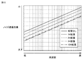
- 7 is a graph showing the noise shielding effect of extending the shield pattern.
- FIG. 8 is a perspective view of a control circuit module according to Modification 1 of Embodiment 1;
- FIG. 15 is a cross-sectional view of a cut plane along line XV-XV of FIG. 14;
- FIG. 8 is a perspective view of a control circuit module according to Modification 2 of Embodiment 1;
- FIG. 17 is a cross-sectional view of a section along line XVII-XVII of FIG. 16;
- FIG. 11 is a perspective view of a control circuit module according to Modification 3 of Embodiment 1;
- FIG. 11 is a top view of the surface of a control circuit module according to Modification 3 of Embodiment 1;
- FIG. 10 is a top view of the rear surface of the control circuit module according to Modification 3 of Embodiment 1;
- FIG. 19 is a cross-sectional view of a section along line XXI-XXI of FIG. 18;
- FIG. 19 is a cross-sectional view of a section along line XXII-XXII of FIG. 18;
- FIG. 11 is a perspective view of a power conversion device according to Embodiment 2;
- FIG. 10 is a top view of a power conversion device according to Embodiment 2;
- FIG. 25 is a cross-sectional view of a cut plane along line XXV-XXV of FIG. 24;
- FIG. 11 is a top view of the surface of a control circuit module according to Embodiment 2;
- FIG. 11 is a top view of the rear surface of the control circuit module according to the second embodiment;
- FIG. 27 is a cross-sectional view of a section along line XXVIII-XXVIII of FIG. 26;
- FIG. 29 is a cross-sectional view of a cut surface corresponding to FIG. 28 of a modified example of the second embodiment
- FIG. 11 is a perspective view of a power conversion device according to Embodiment 3
- FIG. 11 is a top view of a power conversion device according to Embodiment 3
- FIG. 32 is a cross-sectional view of a section along line XXXII-XXXII of FIG. 31
- FIG. 11 is a perspective view of a power conversion device according to Embodiment 4
- FIG. 12 is a top view of a power conversion device according to Embodiment 4
- Figure 35 is a cross-sectional view of the cut plane along line XXXV-XXXV of Figure 34;
- FIG. 14 is a top view of the back surface of the control circuit module according to the fourth embodiment;
- FIG. 11 is a top view of a power conversion device according to Embodiment 5;
- FIG. 11 is a top view of the surface of a control circuit module according to Embodiment 5;
- FIG. 20 is a top view of the back surface of the control circuit module according to the fifth embodiment;
- FIG. 39 is a cross-sectional view of a cut plane along line XL-XL of FIG. 38;
- FIG. 11 is a top view of a power conversion device according to Embodiment 6;
- FIG. 12 is a perspective view of a power conversion device according to Embodiment 7;
- FIG. 11 is a top view of a power conversion device according to Embodiment 7;
- FIG. 44 is a cross-sectional view of a section along line XLIV-XLIV of FIG. 43;
- FIG. 1 is a circuit diagram showing an example of a power converter according to Embodiment 1.
- FIG. 1 is a circuit diagram showing an example of a power converter according to Embodiment 1.
- the power converter 1 shown in FIG. 1 is a DC/DC converter.
- the power converter 1 includes an inverter circuit 2 , a transformer circuit 3 , a rectifier circuit 4 , a smoothing circuit 5 and a control circuit 100 .
- the power conversion device 1 converts a DC voltage Vi input from an input terminal 10 into a DC voltage Vo and outputs the DC voltage Vo from an output terminal 11 .
- the inverter circuit 2 includes switching elements 7a, 7b, 7c, and 7d.
- Each of the switching elements 7a, 7b, 7c, and 7d is a MOSFET (Metal Oxide Semiconductor Field Effect Transistor) or an IGBT (Insulated Gate Bipolar Transistor).
- MOSFET Metal Oxide Semiconductor Field Effect Transistor
- IGBT Insulated Gate Bipolar Transistor
- Each of switching elements 7a, 7b, 7c, and 7d is made of silicon (Si), silicon carbide (SiC), gallium nitride (GaN), or the like.
- the transformer circuit 3 has a transformer 21 .
- the transformer 21 includes a primary high-voltage winding connected to the inverter circuit 2, a core material such as ferrite, and a secondary low-voltage winding.
- the rectifier circuit 4 includes diodes 8a, 8b, 8c, and 8d.
- Diodes 8a, 8b, 8c, and 8d are each made of Si, SiC, GaN, or the like.
- the smoothing circuit 5 includes a smoothing coil 20 and a capacitor 9a.
- the control circuit 100 includes a control element 101 for generating and outputting a control signal for controlling the inverter circuit 2, a connecting member 102 such as a connector for connecting to the inverter circuit 2, and a feedback connector for detecting the DC voltage Vo. and electronic components such as capacitors or resistors.
- the pulse transformer circuit 6 includes pulse transformers 22a and 22b.
- the pulse transformer circuit 6 electrically isolates the control signal output from the control circuit 100 and controls the switching elements 7a, 7b, 7c, and 7d of the inverter circuit 2.
- a printed circuit board is attached to the support.
- the support is a housing of the power converter 1 .
- the housing is made of metal and also serves as a cooler.
- a ground (GND) of the power converter 1 is connected to the support.
- Other electronic components may be mounted on the printed circuit board.
- the power conversion device 1 outputs a DC voltage Vo of 12V to 16V, for example.
- the DC voltage Vi input to the input terminal 10 is converted into a first AC voltage by the inverter circuit 2 and the control circuit 100 that controls it.
- the first AC voltage is converted by the transformer circuit 3 into a second AC voltage lower than the first AC voltage.
- the second AC voltage is rectified by rectifier circuit 4 .
- Smoothing circuit 5 smoothes the voltage output from rectifying circuit 4 .
- the power converter 1 outputs the DC voltage Vo output from the smoothing circuit 5 from the output terminal 11 .
- the DC voltage Vo is fed back to the control circuit 100.
- the control circuit 100 generates a control signal according to the DC voltage Vo, controls the inverter circuit 2, and specifies the DC voltage Vo. keep the value.
- the time change of voltage (dV/dt), time change of current (di /dt) becomes a source of noise.
- Noise is radiated from circuit wiring on a printed circuit board connected to these electronic components. Radiated noise is induced into nearby circuits.
- a different control signal is output.
- the timing for controlling the switching elements 7a, 7b, 7c, and 7d in the inverter circuit 2 changes.
- the DC voltage Vo may fluctuate.
- the switching elements 7a, 7c, or 7b, 7d are turned on at the same time, causing an overcurrent to flow through the switching elements 7a, 7b, 7c, 7d. Doing so may damage the product.
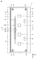
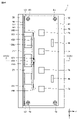
- FIG. 2 is a perspective view of the power converter 1 according to Embodiment 1.
- FIG. 3 is a top view of FIG. 2.
- FIG. 4 is a cross-sectional view of a cut plane along line IV-IV of FIG. 3.
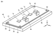
- FIG. 5 is a perspective view of the first printed circuit board module 40 included in the power converter 1.
- FIG. 6 is a perspective view of the second printed circuit board module 50 included in the power converter 1. As shown in FIG.
- the power converter 1 includes a housing 30, a first printed board module 40, a second printed board module 50, and a control circuit module 100a. .
- the first printed circuit board module 40 and the second printed circuit board module 50 are electrically connected by a harness (not shown) or the like.
- the power conversion device 1 includes two printed circuit board modules, but may include three printed circuit board modules.
- the power conversion device 1 includes a housing 30, a first printed circuit board 41, a first insulating member 42, a first fixing member 43, a second printed circuit board 51, A second insulating member 52, a second fixing member 53, a control circuit board 100b as a board of the control circuit module 100a, a connection member 102, and a connection member 103 are provided.
- an external cooling body (not shown) is connected to the bottom surface of the housing 30, for example, to the bottom surface of the portion where the first printed circuit board 41 is fixed. Thereby, heat dissipation is excellent.
- Switching elements 7a, 7b, 7c, and 7d are mounted on the first printed circuit board 41 as electronic components that generate a large amount of heat.
- the housing 30 has at least two inner surfaces. In this embodiment, the housing 30 has two inner surfaces. The housing 30 is configured such that two inner surfaces intersect with each other.
- the first printed circuit board 41 is fixed to the inner surface of the housing 30 .
- the first printed circuit board 41 has a front surface on which electronic components are mounted and a back surface facing the housing 30 .
- the first insulating member 42 is arranged between the first printed circuit board 41 and the housing 30 .
- the first printed circuit board 41 is thermally connected to the housing 30 .
- the first fixing member 43 is configured to fix the first printed circuit board 41 to the housing 30 .
- the first printed circuit board 41 is connected to the housing 30 by a first fixing member 43 .
- the second printed circuit board 51 is fixed to the inner surface of the housing 30 .
- the second printed circuit board 51 is arranged so as to cross the first printed circuit board 41 .
- the second printed circuit board 51 is arranged perpendicular to the first printed circuit board 41 .
- the second printed circuit board 51 has a front surface on which electronic components are mounted and a back surface facing the housing 30 .
- the second printed circuit board 51 is electrically connected to the first printed circuit board 41 by a connecting member (not shown).
- the second insulating member 52 is arranged between the second printed circuit board 51 and the housing 30 .
- the second printed circuit board 51 is thermally connected to the housing 30 .
- the second fixing member 53 is configured to fix the second printed circuit board 51 to the housing 30 .
- the second printed board 51 is connected to the housing 30 by a second fixing member 53 .
- the control circuit board 100 b is arranged along the second printed circuit board 51 .
- the control circuit board 100b is arranged perpendicular to the first printed circuit board 41 on which the switching elements 7a, 7b, 7c, and 7d are mounted, and parallel to the second printed circuit board 51. ing.
- the control circuit board 100b is fixed and electrically connected to the first printed circuit board 41 by a connecting member 102 such as a connector.
- the housing 30 has a thermal conductivity of 1.0 W/(m ⁇ K) or more, preferably 10.0 W/(m ⁇ K) or more, and more preferably 100.0 W/(m ⁇ K) or more.
- the housing 30 is made of metal material such as copper, iron, aluminum, iron alloy, aluminum alloy.
- the housing 30 may include piping for passing cooling water inside.
- the housing 30 may be provided with heat radiating fins or the like in order to promote heat radiation to the surrounding atmosphere. Further, the housing 30 may be in contact with an external cooling body (not shown).
- the housing 30 is not necessarily integrally molded, but may be three-dimensionally formed by combining a plurality of metal plates and connecting them.
- the first printed circuit board 41 and the second printed circuit board 51 may have circuit wiring (not shown) formed on their surface or inside.
- the control circuit board 100b may include at least two conductor layers, and circuit wiring (not shown) may be formed on the surface or inside thereof.
- This circuit wiring has a thickness of 1 ⁇ m or more and 2000 ⁇ m or less.
- this circuit wiring is formed from a conductive material such as copper, nickel, gold, aluminum, silver, tin, or an alloy thereof.
- the materials constituting the printed circuit boards such as the first printed circuit board 41, the second printed circuit board 51, the control circuit board 100b, etc.
- the first printed circuit board 41, the second printed circuit board 51, and the control circuit board 100b may be made of a material generally considered to have low thermal conductivity. That is, each of the first printed circuit board 41, the second printed circuit board 51, and the control circuit board 100b may be a general-purpose printed circuit board. Also, each of the first printed circuit board 41, the second printed circuit board 51, and the control circuit board 100b may be made of ceramics such as aluminum oxide, aluminum nitride, and silicon carbide.
- the first insulating member 42 and the second insulating member 52 have electrical insulation. Also, the first insulating member 42 and the second insulating member 52 may have elasticity. Also, the first insulating member 42 and the second insulating member 52 may have a Young's modulus of 1 MPa or more and 100 MPa or less. The first insulating member 42 and the second insulating member 52 have a thermal conductivity of 0.1 W/(m ⁇ K) or more, preferably 1.0 W/(m ⁇ K) or more.
- the first insulating member 42 and the second insulating member 52 are, for example, rubber materials such as silicone and urethane, and resin materials such as acrylonitrile-butadiene-styrene (ABS), polybutylene terephthalate (PBT), polyphenylene sulfanide (PPS), and phenol. , a polymeric material such as polyimide, a ceramic material such as alumina (aluminum oxide) or aluminum nitride, a phase change material containing silicone as a main raw material, or the like. Also, the first insulating member 42 and the second insulating member 52 may be made of a material in which particles of aluminum oxide, aluminum nitride, boron nitride, or the like are mixed in silicone resin.
- the material of the first fixing member 43 and the second fixing member 53 may be metal or non-metal.
- a metal fixing member is used. and the circuit wiring is electrically connected.
- a nonmetallic fixing member such as a resin screw may be used.
- the first fixing member 43 and the second fixing member 53 may be selectively used according to product specifications.
- FIG. 5 An example of the first printed circuit board module 40 and the second printed circuit board module 50 will be described with reference to FIGS. 5 and 6.
- FIG. 5 An example of the first printed circuit board module 40 and the second printed circuit board module 50 will be described with reference to FIGS. 5 and 6.
- the first printed circuit board module 40 includes a first printed circuit board 41, a first insulating member 42, a first fixing member 43, and an electronic component (first component).
- An electronic component (first component) is mounted on the first printed circuit board 41 .
- the electronic parts (first parts) include switching elements 7a, 7b, 7c, and 7d, which are particularly heat-generating parts, a capacitor 9b, an input terminal 10 (not shown), and pulse transformers 22a and 22b (not shown).
- the first insulating member 42 is provided between the first printed circuit board 41 and the housing 30 .
- the first insulating member 42 is preferably in surface contact with the first printed circuit board 41 and the housing 30 .
- the first fixing member 43 fixes the first printed circuit board 41 to the housing 30 .
- the second printed circuit board module 50 includes a second printed circuit board 51, a second insulating member 52, a second fixing member 53, and an electronic component (second component).
- Electronic components (second components) are mounted on the second printed circuit board 51 .
- the electronic parts (second parts) are the transformer 21, the diodes 8a, 8b, 8c, 8d, the smoothing coil 20, the capacitor 9a, the output terminal 11, and the like.
- the second printed circuit board 51 may be mounted with electronic components that constitute the power converter, except for the switching elements 7a, 7b, 7c, and 7d and the control circuit 100.
- the second insulating member 52 is provided between the second printed circuit board 51 and the housing 30 .
- the second insulating member 52 is preferably in surface contact with the second printed circuit board 51 and the housing 30 .
- the second fixing member 53 fixes the second printed circuit board 51 to the housing 30 .
- FIG. 2 to 6 illustrate the case where there are two printed board modules, that is, the first printed board module 40 and the second printed board module 50.
- FIG. When there are three or more printed circuit board modules on which electronic components are mounted, the second printed circuit board module 50 and the Nth printed circuit board module 40 except for the switching elements 7a, 7b, 7c, and 7d mounted on the first printed circuit board module 40 (N is 3 or more) may optionally be mounted with other electronic components.
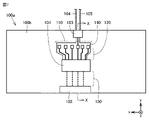
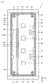
- FIG. 7 is a perspective view of a control circuit module 100a included in the power converter 1.
- FIG. 8 is a top view of the front surface of the control circuit module 100a of FIG. 7, and
- FIG. 9 is a top view of the back surface of the control circuit module 100a of FIG. 10 is a cross-sectional view of a cut plane along line XX of FIG. 7.
- FIG. FIG. 11 is a cross-sectional view taken along the line XX in FIG. 7 when the control circuit board 100b is not a double-sided board but a multi-layer board. 7 to 11 are schematic diagrams of the control circuit module 100a.
- the control circuit module 100a includes a control circuit board 100b, a control element 101, a connection member 102, a connection member 103, a feedback wiring 104, a reference GND wiring 105, and an electronic circuit for control elements. and a component 110 .
- the control circuit board 100 b includes an analog signal wiring group (circuit wiring) 120 , a digital signal wiring group 130 and a shield pattern 140 .
- the control element 101 is a semiconductor element that outputs control signals for controlling the switching elements 7a, 7b, 7c, and 7d.
- the control signal output by the control element 101 depends on the control method of the power conversion device 1, but for example, switching frequency, duty ratio, dead time, etc. can be cited as design parameters.
- the control element 101 changes the waveform of the control signal according to the potential difference of the feedback wiring 104 with respect to the reference GND wiring 105 or the shield pattern 140 having the same potential as the reference GND wiring 105 and the components of the control element electronic component 110 or their constants. change.
- connection member 102 fixes the control circuit module 100a and the first printed circuit board module 40 together.
- the connection member 102 transmits control signals between the control circuit board 100b and the first printed circuit board 41 .
- the connection members 102 are, for example, board-to-board connectors, mounting sockets, fingers, clips, and the like.
- the connection member 102 may be a combination of a connection member such as a board-to-board connector mounted on the control circuit board 100b and a printed board having circuit wiring separate from the control circuit board 100b.
- the connection member 102 in FIG. 7 is one structure, the connection member 102 may be divided into a plurality of pieces and attached.
- the mounting positions thereof may be arranged on at least one side or more of the side connected to the first printed circuit board 41 in the control circuit board 100b.
- connection member 103 connects the feedback wiring 104 for monitoring the DC voltage Vo in the vicinity of the output terminal 11 of the power converter 1 and the reference GND wiring 105 connected to the GND of the output terminal 11 to the control circuit board 100b.
- the connection members 103 may be structural components such as, for example, terminal blocks, board-to-board connectors, mounting sockets, fingers, clips, and the like.
- the feedback wiring 104 or the reference GND wiring 105 is an electric wire, they may be connected by soldering.
- the connection member 103 in FIG. 7 is integrated, the connection member 103 may be divided into a plurality of pieces and attached. The position of the connecting member 103 is not uniquely limited.
- the feedback wiring 104 connects between the vicinity of the output terminal 11 of the power converter 1 and the connection member 103 .
- feedback trace 104 may be a cable or a board-to-board connector.
- the reference GND wiring 105 connects between the vicinity of the output terminal 11 of the power converter 1 and the connection member 103 .
- the reference GND wiring 105 may be a cable or an inter-board connector.
- the reference GND wiring 105 is called GND, but its potential is not limited to ground or frame GND.
- a reference GND wiring 105 provides a reference potential for defining the potential of the feedback wiring 104 .
- the potential of the reference GND wiring 105 is the GND potential, in other words, the same potential as the housing 30. .
- the control element electronic component 110 is an electronic component connected to the control element 101 .
- the control element electronic component 110 is, for example, a chip resistor, a ceramic capacitor, or the like.
- the type of parts to be mounted, the arrangement of parts, the number of parts, etc. depend on the circuit specifications of the output destinations, such as the control element 101, driver elements (not shown) to which the control signals are output, the pulse transformer circuit 6, the switching elements 7a, 7b, 7c, and 7d. , and electronic components (not shown) may be mounted.
- the analog signal wiring group 120 is for setting the switching frequency, duty ratio, dead time, etc. of control signals for controlling the control element 101 and the switching elements 7a, 7b, 7c, and 7d mounted on the first printed circuit board 41. It is a circuit wiring between the electronic components 110 for control elements. Circuit wiring between the control element 101 and the connecting member 103 also corresponds to the analog signal wiring group 120 .
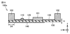
- the wiring layer of the analog signal wiring group 120 may be the surface layer or the inner layer of the printed circuit board. However, the analog signal wiring group 120 has a structure facing the shield pattern 140 described later in a different layer.
- the wiring area of the analog signal wiring group 120 is wired inside at least one time (1H) the thickness H of the insulating layer 150 provided between the opposing shield pattern 140 . It is desirable that the wiring region of the analog signal wiring group 120 be wired inside by three times (3H) or more the thickness H of the insulating layer 150 .
- the analog signal wiring group 120 unintentionally functions as an antenna that receives a magnetic field due to parasitic inductance and mutual inductance with a noise radiation source, or an antenna that receives an electric field due to parasitic capacitance with a noise radiation source. As a result, noise is superimposed on the circuit wiring. As a result, a control signal different from the original design specification may be output, so the analog signal wiring group 120 needs to have a wiring specification that makes it particularly difficult for noise to be superimposed.
- the digital signal wiring group 130 is wiring for transmitting control signals.
- the digital signal wiring group 130 is wiring between the control element 101 and the connection member 102 .
- the wiring layer of the digital signal wiring group 130 may be a surface layer or an inner layer, and is not limited.
- An electronic component such as a driver IC (Integrated Circuit) may be mounted between the control element 101 and the connection member 102 .
- the shield pattern 140 is circuit wiring having the same potential as the reference GND wiring 105 .
- the potential of the shield pattern 140 is the same potential as the ground of the control circuit board 100b.
- the potential of the ground of the control circuit board 100b is the same as that of the housing 30 .
- the shield pattern 140 may be provided at least on the control circuit board 100b, and is necessarily provided on the first printed board module 40 and the second printed board module 50, as well as the third printed board module 60, the fourth printed board module 70 and It does not have to be provided for each printed circuit board that constitutes the fifth printed circuit board module 80 .
- the shield pattern 140 faces the analog signal wiring group 120 on a layer different from the analog signal wiring group 120 .
- the shield pattern 140 at least partially overlaps the analog signal wiring group 120 when viewed from the opposite direction in which the shield pattern 140 faces the analog signal wiring group 120 .
- the shield pattern 140 is the smallest region that faces the analog signal wiring group 120 in a layer different from that of the analog signal wiring group 120, a circuit wiring having the same potential as the shield pattern 140 is placed directly under a signal wiring group different from the analog signal wiring group 120, for example. There may be Also, there may be circuit wiring having the same potential as the shield pattern 140 in the same layer as the analog signal wiring group 120 .
- the shield pattern 140 is expanded more than the analog signal wiring group 120 when viewed from the opposing direction in which the shield pattern 140 faces the analog signal wiring group 120 . That is, the projected area of the shield pattern 140 covers the wiring area of the analog signal wiring group 120 and protrudes outward from the outer end of the wiring area of the analog signal wiring group 120 .
- the shield pattern 140 is at least 1 times thicker than the thickness H of the insulating layer 150 between the wiring layer of the analog signal wiring group 120 and the shield pattern 140 from the wiring area end of the analog signal wiring group 120 .
- a circuit wiring extended by (1H) is provided in a layer different from the analog signal wiring group 120 .
- the analog signal wiring group 120 is wired at least 1H inside the wiring area of the shield pattern 140 facing it.
- the shield pattern 140 when viewed from the opposite direction in which the shield pattern 140 faces the analog signal wiring group 120, the shield pattern 140 is positioned between the analog signal wiring group 120 and the shield pattern 140 in the facing direction with respect to the outer end of the analog signal wiring group 120. is expanded by three times or more of the thickness H between That is, the projected area of the shield pattern 140 covers the wiring area of the analog signal wiring group 120 and protrudes outside by three times or more the thickness H from the outer end of the wiring area of the analog signal wiring group 120 .
- a double-sided board has a board thickness of 1.6 mm and the analog signal wiring group 120 is wired on the component side.
- the shield pattern 140 has circuit wiring extending from the end of the analog signal wiring group 120 by 3H, that is, by 4.8 mm (3 ⁇ 1.6 mm) on the solder surface.
- the thickness H of the insulating layer 150 becomes relatively thin as the number of layers increases in the multi-layer substrate and the wiring layers of the analog signal wiring group 120 and the shield pattern 140 are placed adjacent to each other.
- the area where the shield pattern 140 is extended can be made smaller than the wiring area.
- the noise component is an electric field
- the electric field on the surface of the shield pattern 140 is only a normal component.
- a high shielding effect can be obtained because the electric field can be reflected due to the difference in the intrinsic impedance of the .
- the noise component is a magnetic field
- the magnetic field is formed not only in the normal direction to the shield pattern 140 but also in an arc-shaped current path that is the noise radiation source.
- the magnetic field has a component with an angle of incidence that depends on the distance from the noise radiation source, and a relatively small normal component.
- the skin depth of non-magnetic metals at low frequencies is deep, it is difficult to attenuate the magnetic field by generating eddy currents. In such a case, according to Faraday's law of electromagnetic induction, the induced voltage due to electromagnetic induction can be suppressed by reducing the magnetic field interlinking the loop formed between the analog signal wiring group 120 and the shield pattern 140. becomes valid.
- control circuit board 100b when the control circuit board 100b is a multilayer board, the analog signal wiring groups 120 on the surface and inner layers of the control circuit module 100a are electrically connected via vias 142.
- the analog signal wiring group 120 is arranged in the inner layer of the printed board, and the shield pattern 140 covers it in the upper and lower layers, thereby obtaining a very high noise shielding effect in all directions.
- the shield pattern 140 covers it in the upper and lower layers, thereby obtaining a very high noise shielding effect in all directions.
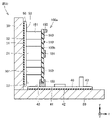
- FIG. 13 shows an example of the effect of suppressing the noise superimposition amount by extending the shield pattern 140 from the wiring area of the analog signal wiring group 120 .
- the noise shielding effect increases as the shield pattern 140 extends from the wiring area end of the analog signal wiring group 120.
- FIG. 13 shows an example of the effect of suppressing the noise superimposition amount by extending the shield pattern 140 from the wiring area of the analog signal wiring group 120 .
- the second printed circuit board 51 is arranged to cross the first printed circuit board 41, and the control circuit board 100b is arranged along the second printed circuit board 51. there is Therefore, the power conversion device 1 can be downsized.
- the shield pattern 140 at least partially overlaps the analog signal wiring group 120 when viewed from the opposite direction in which the shield pattern 140 faces the analog signal wiring group 120 . Therefore, the shield pattern 140 can block noise. Therefore, it is possible to provide the control circuit board 100b with excellent noise immunity. As a result, it is possible to provide the power conversion device 1 that is excellent in noise resistance and is less likely to malfunction.
- the shield pattern 140 is extended beyond the analog signal wiring group 120 when viewed from the facing direction in which the shield pattern 140 faces the analog signal wiring group 120 . Therefore, it is possible to shield not only noise that is incident perpendicularly to the shield pattern 140 but also noise that is incident obliquely. As a result, superposition of noise on the analog signal wiring group 120 can be suppressed.
- the parasitic inductance of the analog signal wiring group 120 can be reduced by making the shield pattern 140 face the analog signal wiring group 120 and providing the circuit wiring extended from the wiring area.
- the mutual inductance between the electronic components mounted on the first printed circuit board 41 or the second printed circuit board 51 and the wiring associated with them can also be reduced.
- inductive coupling between the analog signal wiring group 120 and the switching elements 7a, 7b, 7c, 7d, etc. can be suppressed, so that the amount of noise superimposed on the analog signal wiring group 120 can be suppressed.
- the shield pattern 140 faces the outer end of the analog signal wiring group 120 when viewed from the facing direction in which the shield pattern 140 faces the analog signal wiring group 120.
- the extension is three times or more the thickness H between the analog signal wiring group 120 and the shield pattern 140 in the direction. Therefore, it is possible to further shield not only the noise incident perpendicularly to the shield pattern 140 but also the noise incident obliquely.
- the potential of the shield pattern 140 is the same potential as the ground of the control circuit board 100b. Therefore, the shield pattern 140 functions as an electrostatic shield that prevents electrostatic coupling.
- the potential of the ground of the control circuit board 100b is the same as that of the housing 30.
- the shield pattern 140 is connected to the housing 30 at the same potential via the reference GND wiring 105, the shield pattern 140 also functions as an electrostatic shield that prevents electrostatic coupling. Therefore, it is possible to provide the control circuit module 100a with excellent noise immunity, and the power conversion device 1 with excellent noise immunity and no malfunction.
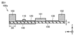
- FIGS. 14 to 22 three types of examples of the control circuit module 100a are shown as modifications of the first embodiment. 14 to 22 differ from the first embodiment in the shape of the shield pattern 140 and the presence/absence of the extended shield pattern 141.
- FIG. 14 is a perspective view of a control circuit module 100a according to Modification 1 of Embodiment 1.
- FIG. 15 is a cross-sectional view of a cut plane along line XV-XV of FIG. 14. FIG. Focusing on the differences from the first embodiment, descriptions of the same configurations, operations and effects will not be repeated.
- the control element 101 in addition to the analog signal wiring group 120, the control element 101 also faces in a different layer.
- the shield pattern 140 is provided between the shield pattern 140 facing the wiring layer of the analog signal wiring group 120 from the wiring area of the analog signal wiring group 120 and the end of the component placement area of the control element 101, and the thickness of the insulating layer 150.
- H is extended by at least one time (1H), preferably three times (3H).
- the analog signal wiring group 120 and the control element 101 are wired at least 3H inside the wiring area of the opposing shield pattern 140 .
- Modification 1 of Embodiment 1 has the advantage that the noise resistance of control element 101, which depends on the chip manufacturer, can be improved by designing control circuit board 100b.
- FIG. 16 is a perspective view of a control circuit module 100a according to Modification 2 of Embodiment 1.
- FIG. 17 is a cross-sectional view of a cut plane along line XVII-XVII of FIG. 16; FIG. Focusing on the differences from the first embodiment, descriptions of the same configurations, operations and effects will not be repeated.
- the shield pattern 140 in Modification 2 of Embodiment 1 is provided on one surface of a layer different from the analog signal wiring group 120, the digital signal wiring group 130, the control element 101, and the like.
- the shield pattern 140 having the same size as the outer shape of the control circuit board 100b is provided to cover all signal wiring and electronic component areas on the control circuit board 100b.
- the shield pattern 140 on one surface of the control circuit board 100b in this manner, not only noise that is incident perpendicularly to the shield pattern 140 but also noise that is incident obliquely can be shielded. As a result, superposition of noise on the analog signal wiring group 120, the digital signal wiring group 130, the control element 101, circuit wiring (not shown), and electronic components can be suppressed.
- FIG. 18 is a perspective view of a control circuit module 100a according to Modification 3 of Embodiment 1.
- FIG. 19 is a top view of the surface of the control circuit module.
- FIG. 20 is a top view of the rear surface of the control circuit module.
- 21 is a cross-sectional view of a section taken along line XXI-XXI of FIG. 18.
- the first printed circuit board 41 on which the switching elements 7a, 7b, 7c, and 7d are mounted has circuit wiring having the same potential as the shield pattern 140 of the control circuit board 100b.
- the control circuit board 100b includes an extended shield pattern 141 for electrically connecting the circuit wiring of the first printed circuit board 41 and the shield pattern 140.
- the first printed board 41 includes circuit wiring (first printed board circuit wiring 41a) having the same potential as the shield pattern 140.
- the control circuit board 100b includes an extended shield pattern 141. As shown in FIG.
- the shield pattern 140 is electrically connected to the circuit wiring (the first printed circuit board wiring 41 a ) and the extension shield pattern 141 .
- the extension shield pattern 141 extends between the connection member 102 and the shield pattern 140 in order to electrically connect the shield pattern 140 of the control circuit board 100b and the circuit wiring having the same potential as the shield pattern 140 of the first printed circuit board 41. Circuit wiring for connection.
- the wiring layer, wiring width, and wiring routing of the extended shield pattern 141 are preferably the same wiring layer as the shield pattern 140, the wiring width covering the wiring area of the digital signal wiring group 130, and the shortest wiring, but are limited to these. However, it is sufficient if the connection member 102 and the shield pattern 140 can be electrically connected as shown in FIG.
- the shield pattern 140 of the control circuit board 100b can be made the same as the shield pattern 140 of the first printed circuit board 41, which is stable with little potential fluctuation.
- the reference GND wiring 105 can also be connected to the potential circuit wiring (first printed circuit board wiring 41a) at a plurality of points. This reduces the impedance of the shield pattern 140, thereby improving the function of the shield pattern 140 as an electrostatic shield. Therefore, the effect of shielding the electric field is enhanced.
- the extended shield pattern 141 by providing the extended shield pattern 141, the effect of reducing switching noise superimposed on the digital signal wiring group 130 is enhanced.
- Spike-shaped noise generated by the switching elements 7a, 7b, 7c, and 7d is superimposed on the digital signal wiring group 130 that propagates control signals for controlling the switching elements 7a, 7b, 7c, and 7d. Since the extended shield pattern 141 is electrically connected to the circuit wiring on the first printed circuit board 41 on which the switching elements 7a, 7b, 7c, and 7d are mounted, the noise superimposed on the digital signal wiring group 130 is transmitted to the switching elements. It also functions as a path returning to 7a, 7b, 7c and 7d.
- noise superimposed on the digital signal wiring group 130 can be prevented from being secondary coupled to the control element 101, the analog signal wiring group 120, etc., which are close to the digital signal wiring group 130.
- FIG. Furthermore, when the extended shield pattern 141 is provided with circuit wiring covering the wiring area of the digital signal wiring group 130 in a different layer, the parasitic inductance of the digital signal wiring group 130 can be reduced. Mutual inductance with the electronic components provided on the substrate 51 and their associated wiring is reduced. As a result, inductive coupling between the digital signal wiring group 130 and the switching elements 7a, 7b, 7c, 7d, etc. can be suppressed, so that the amount of noise superimposed on the digital signal wiring group 130 can be suppressed.
- Embodiment 2 Next, the power conversion device 1 according to Embodiment 2 will be described with reference to FIGS. 6 and 23 to 29.
- FIG. The second embodiment has the same configuration, operation and effects as those of the first embodiment unless otherwise specified. Therefore, the same reference numerals are given to the same configurations as in the above-described first embodiment, and description thereof will not be repeated.
- the power conversion device 1 according to the second embodiment basically has the same configuration as the power conversion device 1 according to the first embodiment.
- FIG. 23 is a perspective view of the power converter 1 according to Embodiment 2.
- FIG. 24 is a top view of the power conversion device 1 according to Embodiment 2.
- FIG. 25 is a cross-sectional view of a cut plane along line XXV-XXV of FIG. 24.
- FIG. 26 to 29 illustrate the control circuit module 100a according to the second embodiment.
- Power converter 1 according to Embodiment 2 includes fixing member 160, spacer 161, extended shield pattern 141 of control circuit module 100a, via 142, and land 143 as compared with Embodiment 1. Points are different.
- the second printed circuit board 51 includes circuit wiring having the same potential as the shield pattern 140 (second printed circuit board circuit wiring 51a).
- the shield pattern 140 is electrically connected to the circuit wiring (second printed circuit board wiring 51a) and the extended shield pattern 141. As shown in FIG.
- a fixing member 160 and a spacer 161 are used to fix the control circuit module 100a to the second printed circuit board module 50 facing it.
- Materials for the fixing member 160 and the spacer 161 are not limited.
- the presence or absence of the extended shield pattern 141, the via 142, and the land 143 is not limited. Therefore, when the fixing member 160 and the spacer 161 are electrically connected in order to have the same potential as the circuit wiring provided on the second printed circuit board 51, the fixing member 160 and the spacer 161 made of metal are used. Just do it.
- the fixing member 160 and the spacer 161 made of non-metal such as resin may be used.
- the fixing member 160 and the spacer 161 may be used only for fixing according to product specifications, or may be used for electrical connection in addition to fixing. Further, as shown in Modification 3 of Embodiment 1, shield pattern 140 may be connected to circuit wiring on the first printed circuit board via extended shield pattern 141 and connection member 102 .
- control circuit module 100a by fixing the control circuit module 100a to the second printed circuit board module 50 with the fixing member 160 and the spacer 161, vibration resistance is enhanced. Furthermore, by fixing the fixing members 160 and the spacers 161 to the second printed circuit board 51 at equal intervals in a well-balanced manner, the control circuit module 100a is resistant to bending. Further, since the control circuit module 100a is fixed to the second printed circuit board module 50, the connection between the control circuit module 100a and the first printed circuit board module 40 does not necessarily need to be structurally firmly fixed. as long as it can be communicated. In other words, a cable or the like can also be used as the connection member 102 .
- control circuit module 100a If fixing member 160 and spacer 161 are made of non-metal, the electrical contribution to control circuit module 100a is the same as in the first embodiment. The following description assumes that
- FIG. 26 is a top view of the surface of the control circuit module 100a according to the second embodiment.
- FIG. 27 is a top view of the rear surface of the control circuit module 100a according to the second embodiment.
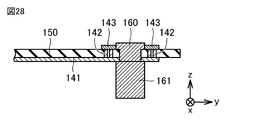
- 28 is a cross-sectional view along line XXVIII-XXVIII of FIG. 26;
- FIG. 29 is a cross-sectional view of a modified example of the control circuit module 100a according to the second embodiment taken along a cut plane corresponding to FIG.
- the control circuit module 100a according to the second embodiment differs from the first embodiment in that the control circuit board 100b includes fixing members 160, vias 142, and lands 143, and the extended shield pattern 141 is modified accordingly. different in that
- the via 142 is for electrically connecting the land 143 on the surface layer of the control circuit board 100 b and the extended shield pattern 141 on a layer different from the land 143 .
- the land 143 is circuit wiring for electrically connecting the extended shield pattern 141 to the fixing member 160 via the via 142 . If the spacer 161 can be electrically connected and structurally fixed to the control circuit board 100b without the fixing member 160, the vias 142 and lands 143 do not necessarily have to be provided, and can be provided arbitrarily according to the connection method. Just do it.
- the extended shield pattern 141 may be a combination of the examples shown in the first embodiment, and is not limited to the illustrated specifications.
- the wiring width of the extended shield pattern 141 is desirably widened, and more desirably it is laid flat on one surface of the control circuit board 100b.
- the extended shield pattern 141 may be connected to the connection member 102 and the GND provided on the first printed circuit board 41 .
- the extension shield pattern 141 and the land 143 may be electrically connected by a passive electronic component 111 such as a capacitor.
- the shield pattern 140 of the control circuit board 100b can be connected at a plurality of points to circuit wiring (second printed circuit board circuit wiring 51a) having the same potential as the shield pattern 140 of the second printed board 51, which is stable with little potential fluctuation. can. This reduces the impedance of the shield pattern 140, thereby improving the function of the shield pattern 140 as an electrostatic shield. Therefore, the effect of shielding the electric field is enhanced.
- Embodiment 3 Next, the power conversion device 1 according to Embodiment 3 will be described with reference to FIGS. 30 to 32.
- FIG. The third embodiment has the same configuration, operation and effect as those of the first and second embodiments unless otherwise specified. Therefore, the same reference numerals are given to the same configurations as in the above-described embodiment, and the description thereof will not be repeated.
- the power converter 1 according to the third embodiment basically has the same configuration as the power converters 1 according to the first and second embodiments.
- FIG. 30 is a perspective view of the power conversion device 1 according to Embodiment 3.
- FIG. 31 is a top view of the power conversion device 1 according to Embodiment 3.
- FIG. 32 is a cross-sectional view of a section taken along line XXXII-XXXII of FIG. 31;
- the power conversion device 1 according to Embodiment 3 differs from Embodiments 1 and 2 in that a holding plate 170 is provided.
- Pressing plate 170 is configured to be thermally connected to electronic components mounted on second printed circuit board 51, such as high heat generating components such as transformer circuit 3 and smoothing coil 20 (see FIG. 1), to cool the electronic components. It is Further, the pressing plate 170 presses and fixes the core material forming the transformer circuit 3 and the smoothing coil 20 against the second printed circuit board 51 .
- the holding plate 170 is arranged between the second printed circuit board 51 and the control circuit board 100b.
- the holding plate 170 is arranged substantially horizontally with the second printed circuit board 51 .
- the pressing plate 170 is configured to press the electronic component against the second printed circuit board 51 . Further, the pressing plate 170 is configured to face the second printed circuit board 51 and the control circuit board 100b.
- the pressing plate 170 has a thermal conductivity of 1.0 W/(m ⁇ K) or more, preferably 10.0 W/(m ⁇ K), more preferably 100.0 W/(m ⁇ K) or more.
- the holding plate 170 is made of metal material such as copper, iron, aluminum, iron alloy, aluminum alloy.
- the holding plate 170 may be provided with radiating fins or the like in order to promote heat radiation to the surrounding atmosphere.
- the restraining plate 170 is not necessarily integrally molded, and may be three-dimensionally formed by combining a plurality of metal plates and connecting them.
- an insulating member similar to the first insulating member 42 and the second insulating member 52 may be provided between the pressing plate 170 and the high heat generating component.
- the restraining plate 170 also functions as a shield for shielding noise from the control circuit module 100a.
- the noise generated by the electronic components fixed by the restraining plate 170 is effectively shielded. Therefore, superposition of noise on the control circuit module 100a can be suppressed. Therefore, the electronic component that generates noise and the control circuit board 100b can be mounted close to each other. As a result, it becomes difficult for noise to be superimposed on the analog signal wiring group 120 and the control element 101 of the control circuit module 100a.
- Embodiment 4 Next, the power conversion device 1 according to Embodiment 4 will be described with reference to FIGS. 33 to 36.
- FIG. The fourth embodiment has the same configuration, operation and effect as those of the first to third embodiments unless otherwise specified. Therefore, the same reference numerals are given to the same configurations as in the above-described embodiment, and the description thereof will not be repeated.
- the power converter 1 according to the fourth embodiment basically has the same configuration as the power converters 1 according to the first to third embodiments.
- FIG. 33 is a perspective view of the power conversion device 1 according to Embodiment 4.
- FIG. 34 is a top view of the power converter 1 according to Embodiment 4.
- FIG. 35 is a cross-sectional view of a section along line XXXV-XXXV of FIG. 34;
- FIG. 36 is a top view of the rear surface of the control circuit module 100a according to the fourth embodiment.
- the power converter 1 according to the fourth embodiment dissipates heat and fixes the electronic components on the second printed circuit board 51 by using the control circuit board 100b instead of the holding plate 170. different in that respect.
- the extended shield pattern 141 on the control circuit board 100b is arranged on the board surface facing the second printed circuit board 51. Points are different.
- a control circuit module 100a according to Embodiment 4 is mounted facing a printed circuit board on which electronic components that need to be heat-dissipated and fixed, such as the second printed circuit board 51 in FIGS. 33 to 35, are mounted.
- the extended shield pattern 141 of the control circuit module 100 a is provided on the surface facing the second printed circuit board 51 .
- the shape and wiring area of the extended shield pattern 141 are not limited.
- circuit wiring is provided on one surface of the control circuit board 100b.
- an insulating member similar to the first insulating member 42 and the second insulating member may be used between the extended shield pattern 141 and the electronic component in order to thermally connect them tightly while insulating them. .
- the control circuit board 100 b is configured to press the electronic components mounted on the second printed board 51 against the second printed board 51 .
- the control circuit board 100 b is arranged substantially horizontally with the second printed circuit board 51 .
- the second printed circuit board 51 and the control circuit board 100b can be mounted close to each other by the volume of the holding plate 170. FIG. Thereby, the power conversion device 1 can be further miniaturized.
- Embodiment 5 Next, the power converter 1 according to Embodiment 5 will be described with reference to FIGS. 37 to 40.
- FIG. The fifth embodiment has the same configuration, operation and effect as those of the first to fourth embodiments unless otherwise specified. Therefore, the same reference numerals are given to the same configurations as in the above-described embodiment, and the description thereof will not be repeated.
- the power converter 1 according to the fifth embodiment basically has the same configuration as the power converters 1 according to the first to fourth embodiments.
- FIG. 37 is a top view of the power converter 1 according to Embodiment 5.
- FIG. FIG. 38 is a top view of the surface of the control circuit module 100a according to the fifth embodiment.
- FIG. 39 is a top view of the rear surface of the control circuit module 100a according to the fifth embodiment.
- 40 is a cross-sectional view along line XL-XL of FIG. 38.
- the power conversion device 1 according to Embodiment 5 includes a printed circuit board module in which electronic components are mounted on the short side of the control circuit board 100b as compared with Embodiments 1 to 4, and these and the third connection member 61 , a fourth connection member 71 , a via 142 and a land 143 .
- the power converter 1 includes a housing 30, a first printed board module 40, a second printed board module 50, a third printed board module 60, and a It has four printed circuit board modules 70, a fifth printed circuit board module 80, and a control circuit module 100a.
- the third printed board module 60, the fourth printed board module 70, and the fifth printed board module 80 are fixed to the housing 30 by printed boards, insulating members, and fixing members, respectively. These printed circuit board modules are electrically connected by a harness (not shown) or the like.
- FIG. 37 which is a top view of the fifth embodiment, the housing 30 has five surfaces, five printed board modules, and the printed board modules are fixed to the inner walls of the housing 30 respectively.
- a printed circuit board module on which electronic components are mounted may be provided as a connection destination of the third connection member 61 or the fourth connection member 71 in addition to the first printed circuit board module 40 . and the number of printed circuit board modules.
- FIG. 37 shows that in the description of the fifth embodiment, as shown in FIG.
- a box-shaped housing 30 having five surfaces, and on each surface thereof, a first printed circuit board module 40, a second printed circuit board module 50, A description will be given assuming that a third printed circuit board module 60, a fourth printed circuit board module 70, and a fifth printed circuit board module 80 are provided.
- the control circuit module 100a is fixed to the third printed board module 60 and the fourth printed board module 70 by the third connection member 61 and the fourth connection member 71, respectively. Although they may or may not be electrically connected, the third connection member 61 and the fourth connection member 71 electrically connect the control circuit module 100a, the third printed circuit board module 60 and the fourth printed circuit board here. A case where the module 70 is connected will be described.
- the third connection member 61 fixes the control circuit board 100b and the third printed circuit board module 60 together.
- the third connection member 61 connects circuit wirings of the same potential of the control circuit board 100b and the third printed circuit board module 60 .
- the third connection member 61 is, for example, a board-to-board connector, mounting socket, finger, clip, or the like. Further, the third connection member 61 may be a connection member obtained by combining a connection member such as an inter-board connector to be mounted on the control circuit board 100b and a printed circuit board.
- the third connection member 61 is one structure in FIG. 37, it may be divided into a plurality of pieces and attached. It may be provided on at least one side connected to the third printed circuit board module 60 .
- the fourth connection member 71 is basically the same as the third connection member 61, but the differences from the third connection member 61 are the fixation to the fourth printed board module 70 and the connection between the control circuit board 100b and the fourth printed board. This is the point for connecting circuit wirings of the same potential of the module 70 .
- the control circuit board 100b can be fixed at a plurality of points, so vibration resistance is excellent.
- the shield pattern 140 on the control circuit board 100b is connected not only to the reference GND wiring 105, but also to the extended shield pattern 141 and the third printed board module 60 and the fourth printed board via the third connection member 61 and the fourth connection member 71. It can be connected to the board module 70 . This reduces the impedance of the shield pattern 140 with respect to the housing 30, thereby improving the function of the shield pattern 140 as an electrostatic shield. Therefore, the effect of shielding the electric field is enhanced.
- Embodiment 6 The power converter 1 according to the sixth embodiment basically has the same configuration as the power converters according to the first to fifth embodiments.
- FIG. 41 is a top view of the power conversion device 1 according to Embodiment 6.
- FIG. The power converter 1 according to Embodiment 6 is different in that the housing 30 has five surfaces and the space surrounded by the housing 30 is filled with the sealing member 180 .
- the power conversion device 1 includes a box-shaped housing 30 having five surfaces, a first printed board module 40 fixed to the inner wall of the housing 30, a second printed board module 50, and a second printed board module 50. It has three printed circuit board modules 60 , a fourth printed circuit board module 70 , a fifth printed circuit board module 80 , a control circuit module 100 a and a sealing member 180 .
- the number of printed circuit board modules is not limited as long as the functions of the power converter 1 can be realized. Here, it is assumed that the number of printed circuit board modules is five from the first printed circuit board module 40 to the fifth printed circuit board module 80 .
- the sealing member 180 fills the space surrounded by the housing 30 . Specifically, the sealing member 180 fills the space surrounded by the box-shaped housing 30 .
- the sealing member 180 includes the first printed board module 40, the second printed board module 50, the third printed board module 60, the fourth printed board module 70, the fifth printed board module 80, and the control circuit module 100a. The electronic components mounted on each are sealed.
- the sealing member 180 may be made of a material having a thermal conductivity of 0.1 W/(m ⁇ K) or more, preferably 1.0 W/(m ⁇ K) or more.
- the sealing member 180 is made of a material having a volume resistivity of 1 ⁇ 10 10 ⁇ m or more, preferably 1 ⁇ 10 12 ⁇ m or more, and more preferably 1 ⁇ 10 14 ⁇ m or more. In other words, the sealing member 180 has electrical insulation.
- the sealing member 180 may have a Young's modulus of 1 MPa or more.
- the sealing member 180 may be made of an elastic resin material.
- the sealing member 180 may be made of a resin material such as polyphenylene sulfide (PPS) or polyetheretherketone (PEEK) containing thermally conductive filler.
- the sealing member 180 may be composed of a rubber material such as silicone or urethane.
- the same effects as those of the power converters 1 according to Embodiments 1 to 5 can be obtained. Furthermore, in the power conversion device 1 according to Embodiment 6, the heat generated by the circuit wiring formed on the surface or inside the printed circuit board and the heat generated by the electronic components mounted on the printed circuit board are dissipated. As the path, a heat radiation path for radiating heat to the housing 30 via the sealing member 180 can be formed. Therefore, it is possible to improve the heat dissipation of the power conversion device 1 for heat generated by the circuit wiring formed on the surface or inside the printed circuit board and heat generated by the electronic components mounted on the printed circuit board. As a result, the power conversion device 1 can operate at high output.
- the power converter 1 according to Embodiment 6 has the first printed board module 40, the second printed board module 50, and the third The size of the printed circuit board module 60, the fourth printed circuit board module 70, and the fifth printed circuit board module 80 can be reduced. Furthermore, the spatial distance between the printed circuit board module and the control circuit module 100a can be shortened. As a result, the power converter 1 according to Embodiment 6 can be miniaturized.
- the sealing member 180 when the sealing member 180 is filled between the printed circuit board and the housing 30, it is possible to eliminate the need for an insulating member arranged between the printed circuit board and the cooling body. Therefore, the number of parts constituting the power converter 1 can be reduced.
- a power converter 1 according to the seventh embodiment is basically a modification of the third embodiment. Moreover, the power converter 1 according to the seventh embodiment has the same configuration as the power converters 1 according to the first and second embodiments.
- FIG. 42 is a perspective view of the power conversion device 1 according to Embodiment 7.
- FIG. 43 is a top view of the power conversion device 1 according to Embodiment 7.
- FIG. 44 is a cross-sectional view of a section taken along line XLIV-XLIV of FIG. 43.
- Power conversion device 1 according to Embodiment 7 is different from Embodiment 3 in that it is not only mounted on second printed circuit board module 50, such as transformer circuit 3 and smoothing coil 20, but also on high-heat generating components such as transformer circuit 3 and smoothing coil 20.
- the holding plate 170 extends to other printed circuit board modules such as the first printed circuit board module 40 .
- the holding plate 170 is arranged between the second printed circuit board 51 and the control circuit board 100b.
- the holding plate 170 extends along the second printed circuit board 51 and extends along the first printed circuit board 41 .
- the pressing plate 170 is arranged substantially horizontally with the second printed circuit board 51 and then curved to extend at least above the first printed circuit board 41 that generates the most heat.
- the structure of the holding plate 170 is at least L-shaped, and by extending to all the printed circuit board modules, it becomes a configuration (bathtub shape) that covers the entire surface of the control circuit board 100b except for one surface. good too.
- the stretched region may be connected to the facing printed circuit board by a fixing member.
- the restraining plate 170 is hollowed out or detoured so as not to physically interfere with the structure.
- the holding plate 170 is configured to be pressed against the electronic components of the second printed circuit board 51 and the first printed circuit board 41 . Further, the pressing plate 170 faces at least the second printed circuit board 51 and also faces the first printed circuit board 41 . The portion of the pressing plate 170 extended to the first printed circuit board 41 is substantially horizontal with the first printed circuit board 41 and substantially perpendicular to the control circuit board 100b.
- the pressing plate 170 has a thermal conductivity of 1.0 W/(m ⁇ K) or more, preferably 10.0 W/(m ⁇ K), more preferably 100.0 W/(m ⁇ K) or more.
- the holding plate 170 is made of metal material such as copper, iron, aluminum, iron alloy, aluminum alloy.
- the holding plate 170 may be provided with radiating fins or the like in order to promote heat radiation to the surrounding atmosphere.
- the restraining plate 170 is not necessarily integrally molded, and may be three-dimensionally formed by combining a plurality of metal plates and connecting them.
- an insulating member similar to the first insulating member 42 and the second insulating member 52 may be provided between the pressing plate 170 and the high heat generating component.
- the suppressing plate 170 covers at least the first printed circuit board module 40 and acts as a shield against noise emitted from the first printed circuit board module 40. Therefore, noise superimposed on the control circuit board 100b is prevented. amount can be suppressed.
- the present embodiment can be applied not only to the high heat generating components such as the transformer circuit 3 and the smoothing coil 20 mounted on the fifth printed circuit board module 80 facing the second printed circuit board module 50, but also to the first printed circuit board.
- a structure in which the pressing plate 170 extends to other printed circuit board modules such as the module 40 may be provided.
- the holding plate 170 is arranged between the fifth printed circuit board module 80 and the control circuit board 100b.
- the pressing plate 170 is arranged substantially horizontally with respect to the fifth printed circuit board module 80 and then curved to extend at least above the first printed circuit board 41 that generates the most heat.
- the pressing plate 170 is configured to be pressed against the electronic components of the fifth printed board module 80 .
- the holding plate 170 faces at least the fifth printed circuit board module 80 and also faces the first printed circuit board 41 .
- 1 power converter 30 housing, 40 first printed board module, 41 first printed board, 50 second printed board module, 51 second printed board, 60 third printed board module, 61 third connection member, 70 third 4 printed circuit board module, 71 fourth connection member, 80 fifth printed circuit board module, 100a control circuit module, 100b control circuit board, 110 electronic components for control elements, 120 analog signal wiring group, 130 digital signal wiring group, 140 shield pattern , 141 expansion shield pattern, 150 insulating layer, 160 fixing member, 170 holding plate, 180 sealing member.
Landscapes
- Engineering & Computer Science (AREA)
- Microelectronics & Electronic Packaging (AREA)
- Power Engineering (AREA)
- Shielding Devices Or Components To Electric Or Magnetic Fields (AREA)
Abstract
Description
まず、実施の形態1に係る電力変換装置について説明する。図1は、実施の形態1に係る電力変換装置の一例を示す回路図である。
制御回路100は、インバータ回路2を制御する制御信号を生成および出力する制御素子101と、インバータ回路2に接続するためのコネクタなどの接続部材102と、直流電圧Voを検出するフィードバック用のコネクタなどの接続部材103と、コンデンサまたは抵抗などの電子部品とを備える。
本実施の形態に係る電力変換装置1によれば、第2プリント基板51は第1プリント基板41と交差するように配置され、制御回路基板100bは第2プリント基板51に沿うように配置されている。このため、電力変換装置1を小型化することができる。また、シールドパターン140がアナログ信号配線群120に対向する対向方向から見て、シールドパターン140はアナログ信号配線群120に少なくとも一部重なっている。このため、シールドパターン140によってノイズを遮断することができる。したがって、ノイズ耐性に優れた制御回路基板100bを提供することができる。ひいては、ノイズ耐性に優れ、誤動作しにくい電力変換装置1を提供することができる。
次に、図6、図23~29図を参照して、実施の形態2に係る電力変換装置1について説明する。実施の形態2は、特に説明しない限り、上記の実施の形態1と同一の構成、動作および効果を有する。したがって、上記の実施の形態1と同一の構成には同一の符号を付し、説明を繰り返さない。
次に、図30~図32を参照して、実施の形態3に係る電力変換装置1について説明する。実施の形態3は、特に説明しない限り、上記の実施の形態1および実施の形態2と同一の構成、動作および効果を有する。したがって、上記の実施の形態と同一の構成には同一の符号を付し、説明を繰り返さない。
次に、図33~図36を参照して、実施の形態4に係る電力変換装置1について説明する。実施の形態4は、特に説明しない限り、上記の実施の形態1~3と同一の構成、動作および効果を有する。したがって、上記の実施の形態と同一の構成には同一の符号を付し、説明を繰り返さない。
次に、図37~図40を参照して、実施の形態5に係る電力変換装置1について説明する。実施の形態5は、特に説明しない限り、上記の実施の形態1~4と同一の構成、動作および効果を有する。したがって、上記の実施の形態と同一の構成には同一の符号を付し、説明を繰り返さない。
実施の形態6に係る電力変換装置1は、基本的には実施の形態1~5に係る電力変換装置と同様の構成を備える。図41は、実施の形態6に係る電力変換装置1の上面図である。実施の形態6に係る電力変換装置1は、筐体30が5面を有し、筐体30に囲まれた空間に、封止部材180が充填されている点で異なる。
実施の形態7に係る電力変換装置1は、基本的には実施の形態3の変形例である。また実施の形態7に係る電力変換装置1は、実施の形態1および実施の形態2に係る電力変換装置1と同様の構成を備える。図42は、実施の形態7に係る電力変換装置1の斜視図である。図43は、実施の形態7に係る電力変換装置1の上面図である。図44は、図43の線XLIV-XLIVに沿う切断面の断面図である。
今回開示された実施の形態はすべての点で例示であって制限的なものではないと考えられるべきである。本開示の範囲は上記した説明ではなくて請求の範囲によって示され、請求の範囲と均等の意味および範囲内でのすべての変更が含まれることが意図される。
Claims (11)
- 少なくとも2面以上の内面を有する筐体と、
前記筐体の前記内面に固定された第1プリント基板と、
前記筐体の前記内面に固定され、前記第1プリント基板と交差するように配置された第2プリント基板と、
前記第2プリント基板に沿うように配置された制御回路基板とを備え、
前記制御回路基板は、回路配線と、前記回路配線とは異なる層において前記回路配線に対向するシールドパターンとを含み、
前記シールドパターンが前記回路配線に対向する対向方向から見て、前記シールドパターンは前記回路配線に少なくとも一部重なっている、電力変換装置。 - 前記対向方向から見て、前記シールドパターンは、前記回路配線よりも拡張されている、請求項1に記載の電力変換装置。
- 前記対向方向から見て、前記シールドパターンは、前記回路配線の外端に対して、前記対向方向での前記回路配線と前記シールドパターンとの間の厚みの3倍以上拡張されている、請求項2に記載の電力変換装置。
- 前記シールドパターンの電位は、前記制御回路基板のグラウンドと同電位である、請求項1~3のいずれか1項に記載の電力変換装置。
- 前記制御回路基板の前記グラウンドの電位は、前記筐体と同電位である、請求項4に記載の電力変換装置。
- 前記第1プリント基板は、前記シールドパターンと同電位の第1プリント基板回路配線を含み、
前記制御回路基板は、拡張シールドパターンを含み、
前記シールドパターンは、前記第1プリント基板回路配線および前記拡張シールドパターンに電気的に接続されている、請求項1~5のいずれか1項に記載の電力変換装置。 - 前記第2プリント基板は、前記シールドパターンと同電位の第2プリント基板回路配線を含み、
前記シールドパターンは、前記第2プリント基板回路配線および前記拡張シールドパターンに電気的に接続されている、請求項6に記載の電力変換装置。 - 前記第2プリント基板に実装された電子部品と、
前記第2プリント基板と前記制御回路基板との間に配置された抑え板をさらに備え、
前記抑え板は、前記電子部品を前記第2プリント基板に対して押し当てるように構成されている、請求項1~7のいずれか1項に記載の電力変換装置。 - 前記抑え板は、前記第2プリント基板に沿うように延在しかつ前記第1プリント基板に沿うように延在している、請求項8に記載の電力変換装置。
- 前記第2プリント基板に実装された電子部品をさらに備え、
前記制御回路基板は、前記電子部品を前記第2プリント基板に対して押し当てるように構成されている、請求項1~7のいずれか1項に記載の電力変換装置。 - 前記筐体により取り囲まれた空間に充填された封止部材をさらに備えた、請求項1~10のいずれか1項に記載の電力変換装置。
Priority Applications (1)
| Application Number | Priority Date | Filing Date | Title |
|---|---|---|---|
| JP2023520992A JPWO2022239698A1 (ja) | 2021-05-11 | 2022-05-02 |
Applications Claiming Priority (2)
| Application Number | Priority Date | Filing Date | Title |
|---|---|---|---|
| JP2021-080372 | 2021-05-11 | ||
| JP2021080372 | 2021-05-11 |
Publications (1)
| Publication Number | Publication Date |
|---|---|
| WO2022239698A1 true WO2022239698A1 (ja) | 2022-11-17 |
Family
ID=84028325
Family Applications (1)
| Application Number | Title | Priority Date | Filing Date |
|---|---|---|---|
| PCT/JP2022/019517 WO2022239698A1 (ja) | 2021-05-11 | 2022-05-02 | 電力変換装置 |
Country Status (2)
| Country | Link |
|---|---|
| JP (1) | JPWO2022239698A1 (ja) |
| WO (1) | WO2022239698A1 (ja) |
Citations (5)
| Publication number | Priority date | Publication date | Assignee | Title |
|---|---|---|---|---|
| JP2016067115A (ja) * | 2014-09-24 | 2016-04-28 | アイシン・エィ・ダブリュ株式会社 | 電力変換装置の制御基板 |
| JP2018152407A (ja) * | 2017-03-10 | 2018-09-27 | ルネサスエレクトロニクス株式会社 | 電子装置 |
| JP2019110711A (ja) * | 2017-12-20 | 2019-07-04 | 株式会社日立製作所 | 電力変換器の制御装置 |
| JP2019176088A (ja) * | 2018-03-29 | 2019-10-10 | 三菱電機株式会社 | プリント基板体 |
| JP2020005365A (ja) * | 2018-06-26 | 2020-01-09 | 株式会社デンソー | スイッチング回路 |
-
2022
- 2022-05-02 WO PCT/JP2022/019517 patent/WO2022239698A1/ja active Application Filing
- 2022-05-02 JP JP2023520992A patent/JPWO2022239698A1/ja active Pending
Patent Citations (5)
| Publication number | Priority date | Publication date | Assignee | Title |
|---|---|---|---|---|
| JP2016067115A (ja) * | 2014-09-24 | 2016-04-28 | アイシン・エィ・ダブリュ株式会社 | 電力変換装置の制御基板 |
| JP2018152407A (ja) * | 2017-03-10 | 2018-09-27 | ルネサスエレクトロニクス株式会社 | 電子装置 |
| JP2019110711A (ja) * | 2017-12-20 | 2019-07-04 | 株式会社日立製作所 | 電力変換器の制御装置 |
| JP2019176088A (ja) * | 2018-03-29 | 2019-10-10 | 三菱電機株式会社 | プリント基板体 |
| JP2020005365A (ja) * | 2018-06-26 | 2020-01-09 | 株式会社デンソー | スイッチング回路 |
Also Published As
| Publication number | Publication date |
|---|---|
| JPWO2022239698A1 (ja) | 2022-11-17 |
Similar Documents
| Publication | Publication Date | Title |
|---|---|---|
| US9406624B2 (en) | Semiconductor module and power converter | |
| JP5259016B2 (ja) | パワー半導体モジュール | |
| US5488256A (en) | Semiconductor device with interconnect substrates | |
| JP2020504459A (ja) | パワーデバイスを並列接続するための低インダクタンスおよび高速スイッチングを有するハイパワー多層モジュール | |
| JP6709810B2 (ja) | 低誘導性ハーフブリッジ装置 | |
| JP6556265B2 (ja) | 回路装置及び電力変換装置 | |
| US11206729B2 (en) | Power circuit device | |
| JP6327113B2 (ja) | 電力変換装置 | |
| JP2022163097A (ja) | トランス及び電力変換装置 | |
| CN111971886A (zh) | 电力转换装置 | |
| WO2022239698A1 (ja) | 電力変換装置 | |
| JP7215316B2 (ja) | 半導体装置 | |
| CN113544958A (zh) | 线圈装置及电力转换装置 | |
| CN110797314A (zh) | 组件 | |
| JPWO2019138861A1 (ja) | コイル装置および電力変換装置 | |
| JP7237475B2 (ja) | パワーモジュール及びスイッチング電源 | |
| TWI677172B (zh) | 緩衝器電路及功率半導體模組以及感應加熱用電源裝置 | |
| JP7345621B2 (ja) | 電力変換装置および電力変換装置の製造方法 | |
| EP3731605A1 (en) | Electric circuit arrangement for a power converter | |
| JP2010251559A (ja) | 電子回路装置 | |
| US11652473B2 (en) | Power modules having an integrated clamp circuit and process thereof | |
| JP6676888B2 (ja) | 電力変換装置 | |
| JP6983277B2 (ja) | 電力変換装置 | |
| US20220344286A1 (en) | Semiconductor module | |
| JP2023115513A (ja) | 電力変換装置 |
Legal Events
| Date | Code | Title | Description |
|---|---|---|---|
| 121 | Ep: the epo has been informed by wipo that ep was designated in this application |
Ref document number: 22807400 Country of ref document: EP Kind code of ref document: A1 |
|
| WWE | Wipo information: entry into national phase |
Ref document number: 2023520992 Country of ref document: JP |
|
| WWE | Wipo information: entry into national phase |
Ref document number: 18554924 Country of ref document: US |
|
| NENP | Non-entry into the national phase |
Ref country code: DE |
|
| 122 | Ep: pct application non-entry in european phase |
Ref document number: 22807400 Country of ref document: EP Kind code of ref document: A1 |