WO2022239681A1 - 半導体集積回路装置 - Google Patents
半導体集積回路装置 Download PDFInfo
- Publication number
- WO2022239681A1 WO2022239681A1 PCT/JP2022/019374 JP2022019374W WO2022239681A1 WO 2022239681 A1 WO2022239681 A1 WO 2022239681A1 JP 2022019374 W JP2022019374 W JP 2022019374W WO 2022239681 A1 WO2022239681 A1 WO 2022239681A1
- Authority
- WO
- WIPO (PCT)
- Prior art keywords
- power supply
- wiring
- supply voltage
- embedded
- cell
- Prior art date
- Legal status (The legal status is an assumption and is not a legal conclusion. Google has not performed a legal analysis and makes no representation as to the accuracy of the status listed.)
- Ceased
Links
Images










Classifications
-
- G—PHYSICS
- G11—INFORMATION STORAGE
- G11C—STATIC STORES
- G11C11/00—Digital stores characterised by the use of particular electric or magnetic storage elements; Storage elements therefor
- G11C11/21—Digital stores characterised by the use of particular electric or magnetic storage elements; Storage elements therefor using electric elements
- G11C11/34—Digital stores characterised by the use of particular electric or magnetic storage elements; Storage elements therefor using electric elements using semiconductor devices
- G11C11/40—Digital stores characterised by the use of particular electric or magnetic storage elements; Storage elements therefor using electric elements using semiconductor devices using transistors
- G11C11/41—Digital stores characterised by the use of particular electric or magnetic storage elements; Storage elements therefor using electric elements using semiconductor devices using transistors forming static cells with positive feedback, i.e. cells not needing refreshing or charge regeneration, e.g. bistable multivibrator or Schmitt trigger
- G11C11/412—Digital stores characterised by the use of particular electric or magnetic storage elements; Storage elements therefor using electric elements using semiconductor devices using transistors forming static cells with positive feedback, i.e. cells not needing refreshing or charge regeneration, e.g. bistable multivibrator or Schmitt trigger using field-effect transistors only
-
- G—PHYSICS
- G11—INFORMATION STORAGE
- G11C—STATIC STORES
- G11C11/00—Digital stores characterised by the use of particular electric or magnetic storage elements; Storage elements therefor
- G11C11/21—Digital stores characterised by the use of particular electric or magnetic storage elements; Storage elements therefor using electric elements
- G11C11/34—Digital stores characterised by the use of particular electric or magnetic storage elements; Storage elements therefor using electric elements using semiconductor devices
- G11C11/40—Digital stores characterised by the use of particular electric or magnetic storage elements; Storage elements therefor using electric elements using semiconductor devices using transistors
- G11C11/41—Digital stores characterised by the use of particular electric or magnetic storage elements; Storage elements therefor using electric elements using semiconductor devices using transistors forming static cells with positive feedback, i.e. cells not needing refreshing or charge regeneration, e.g. bistable multivibrator or Schmitt trigger
- G11C11/413—Auxiliary circuits, e.g. for addressing, decoding, driving, writing, sensing, timing or power reduction
- G11C11/417—Auxiliary circuits, e.g. for addressing, decoding, driving, writing, sensing, timing or power reduction for memory cells of the field-effect type
-
- G—PHYSICS
- G11—INFORMATION STORAGE
- G11C—STATIC STORES
- G11C11/00—Digital stores characterised by the use of particular electric or magnetic storage elements; Storage elements therefor
- G11C11/21—Digital stores characterised by the use of particular electric or magnetic storage elements; Storage elements therefor using electric elements
- G11C11/34—Digital stores characterised by the use of particular electric or magnetic storage elements; Storage elements therefor using electric elements using semiconductor devices
- G11C11/40—Digital stores characterised by the use of particular electric or magnetic storage elements; Storage elements therefor using electric elements using semiconductor devices using transistors
- G11C11/41—Digital stores characterised by the use of particular electric or magnetic storage elements; Storage elements therefor using electric elements using semiconductor devices using transistors forming static cells with positive feedback, i.e. cells not needing refreshing or charge regeneration, e.g. bistable multivibrator or Schmitt trigger
- G11C11/413—Auxiliary circuits, e.g. for addressing, decoding, driving, writing, sensing, timing or power reduction
- G11C11/417—Auxiliary circuits, e.g. for addressing, decoding, driving, writing, sensing, timing or power reduction for memory cells of the field-effect type
- G11C11/419—Read-write [R-W] circuits
-
- G—PHYSICS
- G11—INFORMATION STORAGE
- G11C—STATIC STORES
- G11C5/00—Details of stores covered by group G11C11/00
- G11C5/14—Power supply arrangements, e.g. power down, chip selection or deselection, layout of wirings or power grids, or multiple supply levels
-
- G—PHYSICS
- G11—INFORMATION STORAGE
- G11C—STATIC STORES
- G11C8/00—Arrangements for selecting an address in a digital store
- G11C8/16—Multiple access memory array, e.g. addressing one storage element via at least two independent addressing line groups
-
- H—ELECTRICITY
- H10—SEMICONDUCTOR DEVICES; ELECTRIC SOLID-STATE DEVICES NOT OTHERWISE PROVIDED FOR
- H10B—ELECTRONIC MEMORY DEVICES
- H10B10/00—Static random access memory [SRAM] devices
- H10B10/12—Static random access memory [SRAM] devices comprising a MOSFET load element
-
- H—ELECTRICITY
- H10—SEMICONDUCTOR DEVICES; ELECTRIC SOLID-STATE DEVICES NOT OTHERWISE PROVIDED FOR
- H10D—INORGANIC ELECTRIC SEMICONDUCTOR DEVICES
- H10D89/00—Aspects of integrated devices not covered by groups H10D84/00 - H10D88/00
- H10D89/10—Integrated device layouts
-
- H—ELECTRICITY
- H10—SEMICONDUCTOR DEVICES; ELECTRIC SOLID-STATE DEVICES NOT OTHERWISE PROVIDED FOR
- H10P—GENERIC PROCESSES OR APPARATUS FOR THE MANUFACTURE OR TREATMENT OF DEVICES COVERED BY CLASS H10
- H10P14/00—Formation of materials, e.g. in the shape of layers or pillars
- H10P14/40—Formation of materials, e.g. in the shape of layers or pillars of conductive or resistive materials
-
- H—ELECTRICITY
- H10—SEMICONDUCTOR DEVICES; ELECTRIC SOLID-STATE DEVICES NOT OTHERWISE PROVIDED FOR
- H10W—GENERIC PACKAGES, INTERCONNECTIONS, CONNECTORS OR OTHER CONSTRUCTIONAL DETAILS OF DEVICES COVERED BY CLASS H10
- H10W20/00—Interconnections in chips, wafers or substrates
- H10W20/01—Manufacture or treatment
-
- H—ELECTRICITY
- H10—SEMICONDUCTOR DEVICES; ELECTRIC SOLID-STATE DEVICES NOT OTHERWISE PROVIDED FOR
- H10W—GENERIC PACKAGES, INTERCONNECTIONS, CONNECTORS OR OTHER CONSTRUCTIONAL DETAILS OF DEVICES COVERED BY CLASS H10
- H10W20/00—Interconnections in chips, wafers or substrates
- H10W20/40—Interconnections external to wafers or substrates, e.g. back-end-of-line [BEOL] metallisations or vias connecting to gate electrodes
Definitions
- the present disclosure relates to a semiconductor memory device with memory cells.
- power supply wiring is provided in a buried interconnect layer instead of conventional power supply wiring provided in a metal wiring layer formed above a transistor. It has been proposed to use a power supply wiring (BPR: Buried Power Rail).
- the power supply wiring of the SRAM cell is composed of the embedded power supply wiring.
- power is supplied to each transistor of an SRAM cell via embedded wiring.
- Co, Ru, W, Mo, etc. are being considered as metals to be used for embedded power wiring in memory cells. These metals have a higher resistance than materials such as Cu used in conventional metal wiring layers provided above transistors. When the resistance value of the power supply wiring increases, problems such as deterioration in performance, reliability, and yield of the semiconductor memory device occur due to power supply voltage drop and the like.
- the area of the semiconductor memory device will increase.
- the embedded power wiring is embedded in the substrate, it cannot be formed in the region where the source, drain and channel of the transistor exist. Therefore, an increase in the wiring width of the embedded power supply wiring leads to an increase in the area of the semiconductor memory device. It is also conceivable to reduce the resistance value by increasing the wiring thickness of the embedded power supply wiring, but there is a limit to increasing the wiring thickness.
- An object of the present disclosure is to suppress an increase in the resistance value of the power supply wiring while using an embedded power supply wiring as the power supply wiring in a semiconductor memory device having memory cells.
- the first and second memory sub-arrays arranged side by side in the first direction are arranged between the first and second memory arrays, and are perpendicular to the first direction in plan view. and a plurality of well tap cells arranged side by side in a second direction, and the first and second memory sub-arrays are formed of a plurality of memory cells arranged in an array and an embedded wiring layer, respectively.
- a first embedded power supply wiring extending in the first direction and supplying a first power supply voltage, the well tap cell being formed in the embedded wiring layer and extending in the first direction; and is electrically connected to the first embedded power supply wiring and formed in a second embedded power supply wiring for supplying the first power supply voltage and in a wiring layer above the embedded wiring layer.
- a first wiring extending in two directions and electrically connected to the second embedded power supply wiring for supplying the first power supply voltage; Supply power voltage.
- the first wiring for supplying the first power supply voltage is formed in the wiring layer above the embedded wiring layer of the well tap cell.
- the first wiring is electrically connected to the first embedded wiring formed in the embedded wiring layer of the memory cell via the second embedded power supply wiring formed in the embedded wiring layer of the well tap cell.
- the present disclosure in a semiconductor memory device having memory cells, it is possible to suppress an increase in the resistance value of the power supply wiring while using the embedded power supply wiring as the power supply wiring.
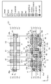
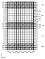
- FIG. 4 is an example of a layout structure of circuit blocks included in the semiconductor memory device according to the present embodiment
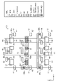
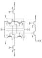
- FIG. 2 is a circuit diagram showing the configuration of a memory cell C1
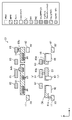
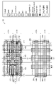
- FIG. 4 is a plan view showing an example of the layout structure of the memory cell C1, where (a) is the upper part of the cell and (b) is the lower part of the cell
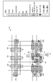
- FIG. 4 is a cross-sectional view showing an example of the layout structure of the memory cell C1
- FIG. 4 is a cross-sectional view showing an example of the layout structure of the memory cell C1
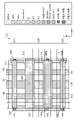
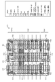
- FIG. 4 is a plan view showing an example of the layout structure of a well tap cell C2
- FIG. 4 is a plan view showing an example of the layout structure of a well tap cell C2
- FIG. 4 is a plan view showing an example of the layout structure of a well tap cell C2;
- FIG. 10 is a plan view showing an example of the layout structure of the BPR tap cell C3, where (a) is the lower part of the cell and (b) is the upper part of the cell; Another example of a circuit block layout structure.
- FIG. 10 is a plan view showing an example of the layout structure of the memory cell C4, where (a) is the upper part of the cell and (b) is the lower part of the cell;
- FIG. 4 is a plan view showing an example of the layout structure of a well tap cell C5;
- FIG. 4 is a plan view showing an example of the layout structure of a well tap cell C5;
- FIG. 10 is a plan view showing an example of the layout structure of a well tap cell C5;
- FIG. 11 is a plan view showing another example of the layout structure of the BPR tap cell C6, where (a) is the cell bottom and (b) is the cell top.
- FIG. 4 is a plan view showing an example of the layout structure of a well tap cell C7;
- FIG. 4 is a plan view showing an example of the layout structure of a well tap cell C7;
- 4 is a circuit diagram showing the configuration of a memory cell C8;
- FIG. FIG. 10 is a plan view showing an example of the layout structure of the memory cell C8, where (a) is the upper part of the cell and (b) is the lower part of the cell;
- FIG. 10 is a plan view showing another example of the layout structure of the well tap cell C9;
- FIG. 10 is a plan view showing another example of the layout structure of the well tap cell C9;
- a semiconductor memory device includes a plurality of memory cells (herein, simply referred to as cells as appropriate), and at least some of the plurality of memory cells are, for example, nanosheet FETs (Field FETs). Effect Transistor).
- a nanosheet FET is an FET that uses a thin sheet (nanosheet) through which current flows.
- the nanosheets are made of silicon, for example.
- a semiconductor layer portion that is formed at both ends of a nanosheet and constitutes a terminal that serves as the source or drain of the nanosheet FET is referred to as a “pad”.
- VDD and VVSS indicate power supply voltage or the power supply itself. Further, in the following description, in plan views such as FIG. Z direction.
- the source and drain of a transistor are appropriately referred to as a "node" of the transistor. That is, one node of a transistor refers to the source or drain of the transistor, and both nodes of the transistor refer to the source and drain of the transistor.
- FIG. 1 is an example of a layout structure of circuit blocks included in a semiconductor memory device according to an embodiment.
- FIG. 1 schematically shows the arrangement of each cell, the embedded power wiring in the embedded wiring layer, and the power wiring in the M2 wiring layer, and the connection relationship between the embedded power wiring and the power wiring in the M2 wiring layer. is shown.
- the well tap cell section A2 is arranged between the upper and lower ends of the drawing of the circuit block and between the memory sub-arrays A1.
- a plurality of memory cells C1 are arranged in each memory sub-array A1. Specifically, in each memory sub-array A1, six memory cells C1 are arranged in the X direction and eight memory cells C1 are arranged in the Y direction. In each memory sub-array A1, the memory cells C1 are alternately arranged in the X direction, with the memory cells C1 arranged in the forward direction and those arranged in the X direction reversed. In each memory sub-array A1, the memory cells C1 arranged in the Y direction are arranged alternately in the forward direction and in the Y direction.
- well tap cells C2 are arranged side by side in the X direction. Although details will be described later, the well tap cell C2 is provided to fix the potentials of the N-well and P-type substrate of each memory cell C1.
- the memory cell C1 arranged in the memory sub-array A1 has a power supply line 11 (12) extending in the Y direction at the boundary with the memory cell C1 adjacent in the X direction.
- the power supply wiring 11 (12) is connected to the power supply wirings 111 (112) and 211 (212) formed in the well tap cell C2 arranged in the well tap cell section A2.
- the power supply wirings 111 (112) and 211 (212) are respectively formed in the embedded wiring layer and connected to the wirings 171 and 271 which are formed in the M2 wiring layer and which supply the power supply voltage VSS. Since the wirings 171 and 271 can strengthen the power supply of the power supply wiring 11 (12) formed in the embedded wiring layer, it is possible to suppress an increase in the resistance value of the power supply wiring while using the embedded power supply wiring as the power supply wiring. can be done.
- FIG. 2 is a circuit diagram showing the configuration of the memory cell C1.
- a memory cell circuit is configured by load transistors PU1 and PU2, drive transistors PD1 and PD2, and access transistors PG1 and PG2.
- Load transistors PU1 and PU2 are P-type FETs
- drive transistors PD1 and PD2 and access transistors PG1 and PG2 are N-type FETs.
- the load transistor PU1 is provided between the power supply voltage VDD and the first node NA, and the drive transistor PD1 is provided between the first node NA and the power supply voltage VSS.
- the load transistor PU1 and the drive transistor PD1 have their gates connected to the second node NB and form an inverter INV1.
- the load transistor PU2 is provided between the power supply VDD and the second node NB, and the drive transistor PD2 is provided between the second node NB and the power supply VSS.
- the load transistor PU2 and the drive transistor PD2 have their gates connected to the first node NA and form an inverter INV2. That is, the output of one inverter is connected to the input of the other inverter, thereby forming a latch.
- the access transistor PG1 is provided between the bit line BL and the first node NA, and has its gate connected to the word line WL.
- the access transistor PG2 is provided between the bit line BLB and the second node NB, and has its gate connected to the word line WL.
- Bit lines BL and BLB form a complementary bit line pair.
- the bit lines BL and BLB are precharged to a high level in advance and the word line WL is driven to a high level
- the bit lines BL and BLB are precharged according to the data written to the first and second nodes NA and NB.
- the data can be read from the memory cell.
- the bit line BL remains at high level and the bit line BLB is discharged to low level.
- the bit line BL is discharged to low level and the bit line BLB keeps high level.
- the memory cell C1 has the functions of writing data to the memory cell, holding data, and reading data from the memory cell by controlling the bit lines BL, BLB and word line WL.
- FIGS. 3 to 5 are diagrams showing an example of the layout structure of the memory cell C1, in which FIGS. 3(a) and 3(b) are plan views, FIGS. b) is a cross-sectional view in the horizontal direction in plan view.
- FIG. 3(a) shows the upper part of the cell, which is the M1 and M2 wiring layers
- FIG. Cell bottom is shown.
- 4(a) is a cross section along line X1-X1'
- FIG. 4(b) is a cross section along line X2-X2'
- FIG. 4(c) is a cross section along line X3-X3'
- FIG. 5(a) is cross section along line X4.
- FIG. 5(b) is the section line X5-X5'.
- the solid lines running vertically and horizontally in plan views such as FIG. 3 and the solid lines running vertically in cross-sectional views such as FIG. 4 indicate grids used for arranging components during design.
- the grids are equally spaced in the X direction and equally spaced in the Y direction.
- the grid spacing may be the same or different in the X direction and the Y direction.
- the grid spacing may be different for each layer.
- each component does not necessarily have to be placed on a grid. However, from the viewpoint of suppressing manufacturing variations, it is preferable to arrange the parts on a grid.
- power supply wirings 11 and 12 extending in the Y direction are formed across the upper and lower ends of the cell in the drawing.
- Each of the power supply wirings 11 and 12 is a buried power supply wiring (BPR: Buried Power Rail) formed in a buried wiring layer.
- BPR Buried Power Rail
- the power supply wirings 11 and 12 are formed on both left and right ends of the cell in the drawing, respectively.
- the power supply wirings 11 and 12 supply the power supply voltage VSS.
- load transistors PU1 and PU2 are formed on the N well 1.
- Access transistor PG 2 and drive transistor PD 2 are formed on P type substrate 2 .
- Drive transistor PD 1 and access transistor PG 1 are formed on P type substrate 3 .
- Nanosheets 21 to 26 extending in the X and Y directions are formed. Nanosheets 21 to 26 form channel portions of access transistor PG2, load transistor PU1, drive transistor PD1, drive transistor PD2, load transistor PU2 and access transistor PG1, respectively.
- Gate wirings (Gates) 31 to 34 extend in the X and Z directions.
- Gate line 31 serves as the gate of access transistor PG2.
- Gate interconnection 32 serves as the gates of load transistor PU1 and drive transistor PD1.
- Gate interconnection 33 serves as the gates of drive transistor PD2 and load transistor PU2.
- Gate interconnection 34 serves as the gate of access transistor PG1.
- Pads 40 doped with N-type impurities are located at the top of the drawing of the nanosheet 21, between the nanosheets 21 and 24, at the bottom of the drawing of the nanosheet 24, at the top of the drawing of the nanosheet 23, between the nanosheets 23 and 26, and at the bottom of the drawing of the nanosheet 26. .about.45 are formed, respectively.
- Pads 40 and 41 form a node of access transistor PG2.
- Pads 41 and 42 form a node of drive transistor PD2.
- Pads 43 and 44 form a node of drive transistor PD1.
- Pads 44 and 45 form a node of access transistor PG1.
- Pads 46 to 49 doped with P-type impurities are formed at the upper end of the drawing of the nanosheet 22, the lower end of the drawing of the nanosheet 22, the upper end of the drawing of the nanosheet 25, and the lower end of the drawing of the nanosheet 25, respectively.
- Pads 46 and 47 constitute the node of load transistor PU1.
- Pads 48 and 49 constitute the node of load transistor PU2.
- Local wiring (LI: Local Interconnect) 51 to 58 extending in the X direction are formed in the local wiring layer.
- Local wiring 51 is connected to pad 40 .
- Local wiring 52 is connected to pad 46 .
- Local wiring 53 is connected to pad 43 .
- Local wiring 54 is connected to pads 41 and 48 .
- Local wiring 55 is connected to pads 47 and 44 .
- Local wiring 56 is connected to pad 42 .
- Local wiring 57 is connected to pad 49 .
- Local wiring 58 is connected to pad 45 .
- the local wiring 56 is connected to the power supply wiring 11 via a contact 81a (Via).
- the local wiring 53 is connected to the power supply wiring 12 via the contact 81b.
- the local wiring 54 is connected to the gate wiring 32 via a shared-contact 82a.
- Local wiring 55 is connected to gate wiring 33 via shared contact 82b.
- Gate interconnection 33, local interconnection 55 and shared contact 82b correspond to first node NA.
- Gate interconnection 32, local interconnection 54 and shared contact 82a correspond to second node NB.
- wirings 61 to 65 are formed in the M1 wiring layer.
- the wirings 61 to 63 extend in the Y direction from the upper and lower ends of the drawing of the cell.
- a wiring 61 supplies a power supply voltage VDD.
- Wirings 62 and 63 correspond to bit lines BLB and BL, respectively.
- the wiring 61 is connected to the local wiring 52 via a contact (Via) 83a, and is connected to the local wiring 57 via a contact 83b.
- the wiring 62 is connected to the local wiring 51 via the contact 83c.
- the wiring 63 is connected to the local wiring 58 via the contact 83d.
- the wiring 64 is connected to the gate wiring 31 via a contact (Gate-contact) 84a.
- the wiring 65 is connected to the gate wiring 34 via the contact 84b.
- a wiring 71 is formed extending in the X direction to both the left and right ends of the cell in the drawing.
- the wiring 71 corresponds to the word line WL.
- the wiring 71 is connected to the wiring 64 via the contact 85a, and is connected to the wiring 65 via the contact 85b.
- each of the nanosheets 21 to 26 consists of three sheet-like semiconductors (nanosheets). That is, each of the nanosheet FETs configured in the memory cell C1 includes three nanosheets.
- the wiring 61 for supplying the power supply voltage VDD is formed in the M1 wiring layer
- the power supply wirings 11 and 12 for supplying the power supply voltage VSS are formed in the embedded wiring layer
- the M2 wiring layer is formed.
- No wiring for supplying the power supply voltages VDD and VSS is provided in the wiring layer. Therefore, the wiring width of the wiring 71 corresponding to the word line WL can be widened. This makes it possible to improve the performance of the semiconductor memory device.
- the power supply wirings 11 and 12 are formed in the embedded wiring layer, and the wiring for supplying the power supply voltage VSS is not provided in the M1 wiring layer. Therefore, the wiring widths of the wirings 62 and 63 (corresponding to the bit lines BLB and BL) can be widened. As a result, the speed of the semiconductor memory device can be increased.
- FIG. 6 and 7 are diagrams showing examples of the layout structure of the well tap cell C2. Specifically, FIG. 6 shows the cell bottom and FIG. 7 shows the cell top.
- the well tap cell C2 consists of a dummy memory cell portion C21 arranged in the upper part and the lower part of the drawing, respectively, and a well tap part C22 arranged in the center of the drawing.
- the dummy memory cell section C21 arranged in the upper part of the drawing is reversed in the Y direction from the dummy memory cell part C21 arranged in the lower part of the drawing.
- the dummy memory cell section C21 has substantially the same layout configuration as the memory cell C1, but the pads 40, 43, and 46 are not formed thereon compared to the memory cell C1. Also, in the M2 wiring layer, a wiring 171 for supplying the power supply voltage VSS is arranged instead of the wiring 71 corresponding to the word line WL. Therefore, each transistor configured in the dummy memory cell section C21 becomes a transistor (dummy transistors dm1 to dm6) having no logic function.
- portions corresponding to the N well 1 and P type substrates 2 and 3 of the memory cell C1 are referred to as an N well 101 and P type substrates 102 and 103, respectively.
- embedded power supply lines corresponding to the power supply lines 11 and 12 of the memory cell C1 are referred to as power supply lines 111 and 112, respectively.
- the dummy memory cell section C21 is arranged adjacent to the memory cell C1 arranged at the Y-direction end of the memory sub-array A1 in the Y direction. Also, the dummy memory cell section C21 has a layout structure substantially similar to that of the memory cell C1. As a result, manufacturing variations in the memory cells C1 arranged at the Y-direction end of the memory sub-array A1 can be suppressed.
- the wiring 171 of the M2 wiring layer with the same wiring width as the wiring 71 (word line WL) of the memory cell C1, the wiring of the M2 wiring layer of the memory cell C1 and the dummy memory cell section C21 can be arranged regularly. can be placed in
- the wiring 171 is connected to the wiring 264 of the M1 wiring layer via the contact 185a, and is connected to the wiring 265 of the M1 wiring layer via the contact 185b.
- the wiring 264 is connected to the power wiring 211 via a contact 283a (283b), a local wiring 251 (252), and a contact 281a (281b), which will be described later.
- the wiring 265 is connected to the power wiring 212 via a contact 283c (283d), a local wiring 253 (254), and a contact 281c (281d) which will be described later.
- the power wiring 211 (212) is connected to the power wiring 11 (12) of the memory cell C1 through the power wiring 111 (112). Accordingly, since the wiring 171 supplies the power supply voltage VSS to the power supply wirings 11 and 12, the power supply of the power supply wirings 11 and 12 of the memory cell C1 can be strengthened.
- the dummy transistors on the N-well 101 are doped with P-type impurities, and the dummy transistors on the P-type substrates 102 and 103 are doped with N-type impurities.
- power supply wirings 211 and 212 are respectively formed at the cell boundaries on the left and right ends of the drawing in the embedded wiring layer.
- nanosheets 221 to 224 extending in the X and Y directions are formed in the well tap portion C22.
- the well tap portion C22 has an N-well formed in the center of the drawing, and P-type substrates are formed on both left and right sides thereof.
- a nanosheet 221 is formed on the P-type substrate 202
- a nanosheet 222 is formed on the P-type substrate 203 .
- Nanosheets 223 and 224 are formed on the N-well 204 .
- Pads 241 to 244 doped with P-type impurities are formed on the top and bottom of the drawing of the nanosheet 221 and the top and bottom of the drawing of the nanosheet 222 .
- Pads 245 to 248 doped with N-type impurities are formed on the upper and lower portions of the nanosheet 223 and the upper and lower portions of the nanosheet 224 .
- Gate wirings 231 to 235 extending in the X and Z directions are arranged. Six gate wirings 231 are arranged at equal intervals between the gate wirings 131 (corresponding to the gate wirings 31 of the memory cell C1) of the dummy memory cell portion C21 in the upper part and the lower part of the drawing. Among the gate wirings 231, the gate wiring 231a overlaps the nanosheet 221 in plan view.
- a gate wiring 232 is arranged adjacent to the gate wiring 132 (corresponding to the gate wiring 32 of the memory cell C1) of the dummy memory cell section C21 in the lower part of the drawing.
- a gate wiring 233 is arranged adjacent to the gate wiring 132 of the dummy memory cell portion C21 in the upper part of the drawing.
- the gate wires 232 and 233 are arranged four gate wires 234 aligned in the Y direction and four gate wires 235 aligned in the Y direction.
- the gate wire 234a overlaps the nanosheets 223 and 224 in plan view.
- the gate wiring 235a overlaps the nanosheet 222 in plan view.
- Local wirings 251 to 256 extending in the X direction are formed in the local wiring layer.
- Local wiring 251 is connected to pad 241 .
- Local wiring 252 is connected to pad 242 .
- Local wiring 253 is connected to pad 243 .
- Local wiring 254 is connected to pad 244 .
- Local wiring 255 is connected to pads 245 and 247 .
- Local wiring 256 is connected to pads 246 and 248 .
- the local wiring 251 is connected to the power supply wiring 211 via a contact 281a.
- the local wiring 252 is connected to the power supply wiring 211 via the contact 281b.
- the local wiring 253 is connected to the power supply wiring 212 via the contact 281c.
- the local wiring 254 is connected to the power supply wiring 212 via the contact 281d.
- wirings 264 and 265 extending in the Y direction are formed in the M1 wiring layer.
- the wiring 264 is connected to the local wiring 251 via the contact 283a, and is connected to the local wiring 252 via the contact 283b.
- the wiring 265 is connected to the local wiring 253 via the contact 283c, and is connected to the local wiring 254 via the contact 283d.
- wirings 271 and 272 extending in the X direction are formed in the M2 wiring layer.
- a wiring 271 is a wiring for supplying the power supply voltage VSS
- a wiring 272 is a wiring for supplying the power supply voltage VDD.
- the wiring 271 is connected to the wiring 264 via the contact 285a, and is connected to the wiring 265 via the contact 285b.
- the wiring 272 is connected to the wiring 61 via the contact 285c.
- the wiring 271 formed in the M2 wiring layer of the well tap portion C22 is embedded via the contact 285a, the wiring 264, the contact 283a (283b), the local wiring 251 (252) and the contact 281a (281b).
- a power supply voltage VSS is supplied to the power supply wiring 211 of the wiring layer.
- the wiring 271 supplies the power supply wiring 212 of the embedded wiring layer with the power supply voltage VSS via the contact 285b, the wiring 265, the contact 283c (283d), the local wiring 253 (254) and the contact 281c (281d).
- the power wiring 211 (212) is connected to the power wiring 11 (12) of the memory cell C1 through the power wiring 111 (112).
- the power supply of the embedded power supply wiring can be strengthened without widening the wiring width of the embedded power supply wiring of the memory cell C1, so an increase in the resistance value of the power supply wiring can be suppressed.
- the wiring 271 supplies the power supply voltage VSS to the local wirings 251-254 and the pads 241-244.
- a P-type substrate 202 is formed below the pads 241 and 242
- a P-type substrate 203 is formed below the pads 243 and 244 .
- Wiring 271 supplies power supply voltage VSS to P-type substrates 202 and 203 via local wirings 251-254 and pads 241-244.
- the wiring 272 supplies the power supply voltage VDD to the local wirings 255 and 256 and the pads 245-248.
- An N-well 204 is formed below the pads 245-248.
- Line 271 supplies power supply voltage VDD to N well 204 via local lines 255 and 256 and pads 245-248.
- the potentials of the N-well 1 and P-type substrates 2 and 3 of the memory cell C1 can be fixed.
- FIG. 8 is an enlarged view of the dotted line segment of the circuit block in FIG.
- FIG. 8 shows the layout structure of the lower part of the cell, and the wirings of the M1 and M2 wiring layers are schematically shown in the upper part and the right side of the drawing.
- the dummy memory cell section C21 is arranged so as to be adjacent to the memory cell C1 arranged at the Y-direction end of the memory sub-array A1, manufacturing variations in the memory cell C1 can be suppressed. can.
- the potentials of the N well 1 and the P type substrates 2 and 3 are fixed.
- the power supply wirings 11, 12, 111, 112, 211, and 212 formed in the embedded wiring layer and the wirings 71, 171, and 271 formed in the M2 wiring layer are configured in a mesh shape in plan view. Therefore, the power supply is strengthened.
- FIG. 9 shows another example of the layout structure of circuit blocks included in the semiconductor memory device according to this embodiment.
- the BPR tap cell section A4 is arranged between the memory sub-arrays A3.
- the BPR tap cell section A4 is arranged between the memory sub-arrays A3.
- Six memory cells C1 are arranged in the X direction and four memory cells C1 are arranged in the Y direction in the memory sub-array A3.
- the memory cells C1 are horizontally reversed in the X direction and vertically reversed in the Y direction.
- BPR tap cells C3 are arranged side by side in the X direction.
- FIG. 10 is a plan view showing an example of the layout structure of the BPR tap cell C3. Specifically, FIG. 10(a) shows the lower part of the cell, and FIG. 10(b) shows the upper part of the cell.
- the BPR tap cell C3 is obtained by omitting the well tap portion C22 from the well tap cell C2 of FIGS.
- local wires 151 and 153 are formed between the dummy memory cell portions C21.
- the local wiring 151 is connected to the power supply wiring 111 via the contact 181a, and is connected to the wiring 264 via the contact 183a.
- the local wiring 153 is connected to the power supply wiring 112 via the contact 181a, and is connected to the wiring 265 via the contact 183a. That is, the wiring 171 formed in the M2 wiring layer is connected to the power supply wiring 111 via the contact 185a, the wiring 264, the contact 183a, the local wiring 151 and the contact 181a. Also, the wiring 171 is connected to the power supply wiring 112 via the contact 185b, the wiring 265, the contact 183b, the local wiring 153 and the contact 181b. As a result, the power supply of the embedded power supply wiring of the memory cell C1 can be strengthened, so that an increase in the resistance value of the power supply wiring can be suppressed.
- FIG. 11 is another example of the layout structure of circuit blocks included in the semiconductor memory device according to the embodiment.
- a power supply wiring 13 for supplying power supply voltage VDD is formed between power supply wirings 11 (12) for supplying power supply voltage VSS in the embedded wiring layer.
- a memory cell C4 is arranged in the memory sub-array A1 instead of the memory cell C1. Also, in the well tap cell section A2, a well tap cell C5 is arranged instead of the well tap cell C2.
- the wiring 272 for supplying the power supply voltage VDD of the M2 wiring layer is connected to the power supply wiring 13 . Since the wiring 272 can strengthen the power supply of the power supply wiring 13, it is possible to suppress an increase in the resistance value of the power supply wiring while using the embedded power supply wiring as the power supply wiring.
- FIG. 12 is a plan view showing an example of the layout structure of memory cell C4.
- FIG. 12(a) shows the upper part of the cell, and
- FIG. 12(b) shows the lower part of the cell.
- the power supply wiring 13 extending in the Y direction is formed in the center of the cell in the embedded wiring layer.
- a power supply wiring 13 supplies a power supply voltage VDD.
- the power supply wiring 13 is connected to the local wiring 52 via the contact 81c, and is connected to the local wiring 57 via the contact 81d.
- the wiring width of the wiring (wiring 61) for supplying the power supply voltage VDD to the M1 wiring layer can be narrowed. Therefore, the distance between the wiring 61 and the wirings 62, 63 (bit lines BLB, BL) can be widened, and the parasitic capacitance can be suppressed. As a result, the speed of the memory cell C4 can be increased. In addition, since the wiring width of the wirings 62 and 63 (bit lines BLB and BL) can be widened and the wiring resistance of the wirings 62 and 63 can be suppressed, the speed of the memory cell C4 can be increased.
- the power supply wiring 13 alone can sufficiently ensure the ability to supply the power supply voltage VDD to the memory cell C4, the wiring 61 of the M1 wiring layer can be omitted.
- FIG. 13 and 14 are plan views showing examples of the layout structure of the well tap cell C5. Specifically, FIG. 13 shows the cell bottom and FIG. 14 shows the cell top.
- an embedded power supply wiring extending in the Y direction is formed in the center of the drawing in the embedded wiring layer.
- the dummy memory cell portion C51 of the well tap cell C5 is formed with the power supply wiring 113
- the well tap portion C52 is formed with the power supply wiring 213.
- the power wiring 213 is connected to the power wiring 13 of the memory cell C4 through the power wiring 113 .
- the power supply wiring 213 is connected to the local wiring 255 via the contact 281e, and is connected to the local wiring 256 via the contact 281f.
- the local wires 255 and 256 are connected to the wire 272 of the M2 wiring layer. That is, the wiring 272 is connected to the power supply wiring 13 of the memory cell C4 through the power supply wirings 213 and 113 .
- the wiring 272 for supplying the power supply voltage VDD formed in the M2 wiring layer supplies the power supply voltage VDD to the power supply wiring 13 of the memory cell C4, so that the power supply of the power supply wiring 13 can be strengthened.
- FIG. 15 is a plan view showing an example of the layout structure of the BPR tap cell C6. Specifically, FIG. 15(a) shows the lower part of the cell, and FIG. 15(b) shows the upper part of the cell.
- the BPR tap cell C6 is obtained by omitting the well tap portion C52 from the well tap cell C2 of FIGS. 13 and 14, and has substantially the same configuration as that of FIG.
- the power supply wiring 113 extending in the Y direction is formed in the center of the drawing in the embedded wiring layer.
- a wiring 173 for supplying the power supply voltage VDD is formed in the M2 wiring layer instead of the wiring 171.
- FIG. The wiring 173 is connected to the wiring 61 via the contact 185e. As described above, the wiring 61 is connected to the power supply wiring 113 via the contact 183b, the local wiring 157 and the contact 181b. That is, the wiring 173 is connected to the power supply wiring 113 .
- the same effect as in FIG. 10 can be obtained. Further, the wiring 173 of the M2 wiring layer can strengthen the power supply of the power supply wiring 13 of the memory cell C4.
- FIGS. 16 and 17 are plan views showing examples of the layout structure of the well tap cell C7.
- Well tap cell C7 of FIGS. 16 and 17 does not have contacts 281e and 281f connecting power supply line 13 and local lines 255 and 256, respectively, as compared with FIGS. That is, the local wirings 255 and 256 are not connected to the power supply wiring 213 .
- a dummy memory cell section C51a is arranged at the top of the drawing.
- a wiring 273 for supplying the power supply voltage VDDB is formed in the M2 wiring layer.
- the wiring 273 is connected to the wiring 61a of the M1 wiring layer through the contact 285e.
- the wiring 61 in the upper part of the drawing and the wiring 61 in the lower part of the drawing are separated, and the wiring 61a is formed between them.
- the wiring 61a is connected to the local wiring 255 via the contact 283e, and is connected to the local wiring 256 via the contact 283f. That is, the wiring 273 supplies the power supply voltage VDDB to the local wirings 255 and 256 .
- the power supply voltage VDDB is supplied to the N well 204 through the local interconnections 255 and 256, the power supply voltage VDDB is supplied to the N well 1 of the memory cell C4.
- the voltage applied to the sources of the load transistors PU1 and PU2 (power supply voltage VDD) and the voltage supplied to the N well 1 (power supply voltage VDDB) can be different voltages. Therefore, even when the circuit block has a power supply control function and the power supply voltages VDD and VDDB are different voltages, it can be handled.
- the well tap cell C7 can obtain the same effect as in FIGS. 13 and 14.
- FIG. 18 is a circuit diagram showing the configuration of memory cell C8.
- memory cell C8 includes load transistors PU1, PU2, drive transistors PD1, PD2, access transistors PG1, PG2, read drive transistor RPD, and read access transistor RPG.
- a memory cell circuit of the port is configured.
- Load transistors PU1 and PU2 are P-type FETs
- drive transistors PD1 and PD2, access transistors PG1 and PG2, read drive transistor RPD and read access transistor RPG are N-type FETs.
- the load transistor PU1 is provided between the power supply voltage VDD and the first node NA, and the drive transistor PD1 is provided between the first node NA and the power supply VSS.
- the load transistor PU1 and the drive transistor PD1 have their gates connected to the second node NB and form an inverter INV1.
- the load transistor PU2 is provided between the power supply voltage VDD and the second node NB, and the drive transistor PD2 is provided between the second node NB and the power supply VSS.
- the load transistor PU2 and the drive transistor PD2 have their gates connected to the first node NA and form an inverter INV2. That is, the output of one inverter is connected to the input of the other inverter, thereby forming a latch.
- the access transistor PG1 is provided between the write bit line WBL and the first node NA, and has its gate connected to the write word line WWL.
- the access transistor PG2 is provided between the write bit line WBLB and the second node NB, and has its gate connected to the write word line WWL.
- Write bit lines WBL and WBLB form a complementary write bit line pair.
- the read drive transistor RPD has a source connected to the power supply VSS, a gate connected to the second node NB, and a drain connected to the source of the read access transistor RPG.
- the read access transistor RPG has a gate connected to the read word line RWL and a drain connected to the read bit line RBL.
- the state of the read bit line RBL is determined according to the data written to the second node NB. , data can be read from the memory cell. Specifically, when the second node NB is at high level, the read bit line RBL is discharged to low level. On the other hand, if the second node NB is at low level, the read bit line RBL maintains high level.
- the memory cell writes data to the memory cell, holds the data, and stores the data in the memory cell by controlling the write bit lines WBL and WBLB, the read bit line RBL, the write word line WWL, and the read word line RWL. It has a function of reading data from
- FIG. 19 is a plan view showing an example of the layout structure of memory cell C8.
- FIG. 19(a) shows the upper part of the cell
- FIG. 19(b) shows the lower part of the cell.
- the memory cell C8 in FIG. 19 has a read drive transistor RPD and a read access transistor RPG formed on the right side of the drawing compared to FIG.
- Nanosheets 27 and 28 are formed on the right side of the nanosheets 23 and 26 in the drawing. Nanosheets 27 and 28 form channel portions of read drive transistor RPD and read access transistor RPG, respectively.
- a gate wiring 35 extending in the X and Y directions is formed on the right side of the gate wiring 34 in the drawing.
- Gate interconnection 32 serves as the gate of read drive transistor RPD, and gate 35 serves as the gate of read access transistor RPG.
- Pads 50a to 50c doped with N-type impurities are formed at the upper end of the nanosheet 27, between the nanosheets 27 and 28, and at the lower end of the nanosheet 28, respectively.
- Pads 50a and 50b form a node of read drive transistor RPD.
- Pads 50b and 50c constitute nodes of read access transistor RPG.
- Local wirings 59 and 60 extending in the X direction are formed in the local wiring layer.
- the local wiring 53 is connected with the pad 50a.
- the local wiring 59 is connected with the pad 50b.
- the local wiring 60 is connected with the pad 50c.
- a wiring 67 corresponding to the read bit line RBL is formed in the M1 wiring layer.
- the wiring 67 is connected to the local wiring 60 via the contact 83e.
- the wiring 62 corresponds to the write bit line WBLB
- the wiring 63 corresponds to the write bit line WBL.
- Wirings 72 and 73 extending in the X direction are formed in the M2 wiring layer.
- the wiring 72 corresponds to the read word line RWL
- the wiring 73 corresponds to the write word line WWL.
- the wiring 72 is connected to the gate 35 via the contact 85c, the wiring 68 and the contact 84c.
- the wiring 73 is connected to the gate wiring 31 via the contact 85a, the wiring 64 and the contact 84a. Also, the wiring 73 is connected to the gate wiring 34 via the contact 85b, the wiring 65 and the contact 84b.
- FIG. 20 and 21 are diagrams showing examples of the layout structure of the well tap cell C9. Specifically, FIG. 20 shows the cell bottom and FIG. 21 shows the cell top.
- the well tap cell C9 in FIGS. 20 and 21 is configured substantially similarly to the well tap cell C2 in FIGS. 6 and 7. Specifically, the well tap cell C9 is composed of a dummy memory cell portion C91 arranged at the upper portion and the lower portion of the drawing, respectively, and a well tap portion C92 arranged at the center of the drawing.
- the dummy memory cell section C91 has almost the same layout configuration as the memory cell C8, but the transistors provided therein are dummy transistors having no logic function. Note that the dummy memory cell portion C91 arranged in the upper part of the drawing is reversed in the Y direction from the dummy memory cell part C91 arranged in the lower part of the drawing.
- wirings 174 and 175 are arranged instead of the wiring 171 in the M2 wiring layer.
- Wirings 174 and 175 each supply a power supply voltage VSS. That is, the wirings 174 and 175 arranged in the M2 wiring layer of the dummy memory cell section C91 are connected to the power wiring 11 (12) of the memory cell C8 via the power wiring 111 (112), respectively.
- the well tap portion C92 has substantially the same configuration as the well tap portion C22 of FIGS. 6 and 7, and strengthens the embedded power supply wiring of the memory cell C8, and the N-well 1 and P-type substrate 2 of the memory cell C8. , 3 are fixed.
- the well tap cell C9 can provide the same effect as the well tap cell C2.
- the well tap cell C9 can be modified to have a configuration similar to that of modified examples 1 and 2.
- the transistor formed in each cell is a nanosheet FET, but it is not limited to this, and may be a fin transistor, for example. Also, although the nanosheet FET of each cell has three nanosheets, the number of nanosheets is not limited to three.
- the memory sub-array A1 has been described as having 6 memory cells arranged in the X direction and 8 memory cells in the Y direction, but the number of memory cells arranged in the array is not limited to this. . The same applies to the number of memory cells arranged in memory sub-array A3.
- the present disclosure since it is possible to suppress an increase in the resistance value of the embedded power supply wiring in the semiconductor memory device using the embedded power supply wiring, it is useful for improving the performance of the semiconductor chip, for example.
Landscapes
- Engineering & Computer Science (AREA)
- Microelectronics & Electronic Packaging (AREA)
- Computer Hardware Design (AREA)
- Power Engineering (AREA)
- Semiconductor Memories (AREA)
- Design And Manufacture Of Integrated Circuits (AREA)
Abstract
メモリセル(C1)はY方向に延びており、電源電圧VSSを供給する電源配線(11)を備える。ウェルタップセル(C2)は、Y方向に延びており、電源配線(11)と電気的に接続されており、電源電圧VSSを供給する電源配線(111,212)と、M1配線層に形成されており、X方向に延びており、電源配線(11)と電気的に接続されており、電源電圧VSSを供給する配線(171,271)とを備える。ウェルタップセル(C2)は、メモリセル(C1)のNウェル(1)またはP型基板(2,3)に電源電圧VSSを供給する。
Description
本開示は、メモリセルを備えた半導体記憶装置に関する。
半導体記憶装置の高集積化のために、従来のようなトランジスタの上層に形成された金属配線層に設けられた電源配線ではなく、埋め込み配線(Buried Interconnect)層に設けられた電源配線である埋め込み電源配線(BPR:Buried Power Rail)を用いることが提案されている。
特許文献1では、SRAMセル(メモリセル)の電源配線が、埋め込み電源配線で構成されている。特許文献1は、埋め込み配線を介して、SRAMセルの各トランジスタに電源が供給される。
メモリセルの埋め込み電源配線に用いられる金属としてはCo、Ru、W、Moなどが検討されている。これらの金属は、トランジスタの上層に設けられる従来の金属配線層に用いられるCuなどの材料よりも抵抗が大きい。電源配線の抵抗値が大きくなると電源電圧降下等により半導体記憶装置の性能低下、信頼性低下、歩留まり低下などの問題が発生する。
ここで、埋め込み電源配線の配線幅を大きくすることにより抵抗値を下げようとした場合には半導体記憶装置の面積が大きくなる。特に、埋め込み電源配線は基板に埋め込まれて形成されているため、トランジスタのソース、ドレインおよびチャネルが存在する領域には形成できない。したがって、埋め込み電源配線の配線幅の増大が半導体記憶装置の面積の拡大へとつながる。また、埋め込み電源配線の配線厚を大きくして抵抗値を下げることも考えられるが、配線厚を大きくすることにも限界がある。
本開示は、メモリセルを備えた半導体記憶装置において、電源配線に埋め込み電源配線を用いつつ、電源配線の抵抗値の増加を抑止することを目的とする。
本開示の態様では、第1方向に並んで配置された第1および第2メモリサブアレイと、前記第1および第2メモリアレイの間に配置されており、平面視において前記第1方向と垂直をなす第2方向に並んで配置された複数のウェルタップセルとを備え、前記第1および第2メモリサブアレイは、それぞれ、アレイ状に配置された複数のメモリセルと、埋め込み配線層に形成されており、前記第1方向に延びており、第1電源電圧を供給する第1埋め込み電源配線とを備え、前記ウェルタップセルは、前記埋め込み配線層に形成されており、前記第1方向に延びており、前記第1埋め込み電源配線と電気的に接続されており、前記第1電源電圧を供給する第2埋め込み電源配線と、前記埋め込み配線層よりも上層の配線層に形成されており、前記第2方向に延びており、前記第2埋め込み電源配線と電気的に接続されており、前記第1電源電圧を供給する第1配線とを備え、前記メモリセルのNウェルまたはP型基板に第2電源電圧を供給する。
この態様によると、ウェルタップセルの、埋め込み配線層よりも上層の配線層には、第1電源電圧を供給する第1配線が形成されている。第1配線は、ウェルタップセルの埋め込み配線層に形成された第2埋め込み電源配線を介して、メモリセルの埋め込み配線層に形成された第1埋め込み配線と電気的に接続されている。これにより、メモリセルの第1埋め込み電源配線の電源を強化することができるため、メモリセルを備えた半導体記憶装置において、電源配線に埋め込み電源配線を用いつつ、電源配線の抵抗値の増加を抑止することができる。また、ウェルタップセルは、メモリセルのNウェルまたはP型基板に第2電源電圧を供給するため、メモリセルのNウェルまたはP型基板の電位を固定することができる。
本開示によると、メモリセルを備えた半導体記憶装置において、電源配線に埋め込み電源配線を用いつつ、電源配線の抵抗値の増加を抑止することができる。
以下、実施の形態について、図面を参照して説明する。以下の実施の形態では、半導体記憶装置は複数のメモリセル(本明細書では、適宜、単にセルという)を備えており、この複数のメモリセルのうち少なくとも一部は、例えば、ナノシートFET(Field Effect Transistor)を備えるものとする。ナノシートFETとは、電流が流れる薄いシート(ナノシート)を用いたFETである。ナノシートは例えばシリコンによって形成されている。また、本開示では、ナノシートの両端に形成されており、ナノシートFETのソースまたはドレインとなる端子を構成する半導体層部のことを「パッド」という。
本開示では、「VDD」「VSS」は、電源電圧または電源自体を示す。また、以下の説明では、図1等の平面図において、図面横方向をX方向(第2方向に相当)、図面縦方向をY方向(第1方向に相当)、基板面に垂直な方向をZ方向としている。
また、本開示では、トランジスタのソースおよびドレインのことを、適宜、トランジスタの「ノード」と称する。すなわち、トランジスタの一方のノードとは、トランジスタのソースまたはドレインのことを指し、トランジスタの両方のノードとは、トランジスタのソースおよびドレインのことを指す。
(実施形態)
(回路ブロックのレイアウト構造)
図1は実施形態に係る半導体記憶装置が備える回路ブロックのレイアウト構造の例である。図1は、各セルの配置と、埋め込み配線層における埋め込み電源配線と、M2配線層における電源配線とを模式的に示したものであり、埋め込み電源配線とM2配線層の電源配線との接続関係を示したものである。
(回路ブロックのレイアウト構造)
図1は実施形態に係る半導体記憶装置が備える回路ブロックのレイアウト構造の例である。図1は、各セルの配置と、埋め込み配線層における埋め込み電源配線と、M2配線層における電源配線とを模式的に示したものであり、埋め込み電源配線とM2配線層の電源配線との接続関係を示したものである。
図1のレイアウトでは、ウェルタップセル部A2は、回路ブロックの図面上端および図面下端ならびにメモリサブアレイA1同士の間に配置されている。
各メモリサブアレイA1には、複数のメモリセルC1(SRAMセル)が配置されている。具体的には、メモリサブアレイA1には、それぞれ、X方向に6つ、Y方向に8つのメモリセルC1がアレイ状に配置されている。また、各メモリサブアレイA1において、メモリセルC1は、X方向において、順方向に配置されたものとX方向に反転させたものとが交互に並んで配置されている。また、各メモリサブアレイA1において、メモリセルC1は、Y方向において、順方向に配置されたものとY方向に反転させたものとが交互に並んで配置されている。
また、ウェルタップセル部A2には、ウェルタップセルC2がX方向に並んで配置されている。詳しくは後述するが、ウェルタップセルC2は、各メモリセルC1のNウェルおよびP型基板の電位を固定するために設けられる。
図1に示すように、メモリサブアレイA1に配置されたメモリセルC1は、X方向に隣接するメモリセルC1との境界に、Y方向に延びる電源配線11(12)が形成されている。詳しくは後述するが、電源配線11(12)は、ウェルタップセル部A2に配置されたウェルタップセルC2に形成された電源配線111(112),211(212)と接続されている。電源配線111(112),211(212)は、それぞれ埋め込み配線層に形成されており、M2配線層に形成された、電源電圧VSSを供給する配線171,271と接続されている。配線171,271により、埋め込み配線層に形成された電源配線11(12)の電源を強化することができるため、電源配線に埋め込み電源配線を用いつつ、電源配線の抵抗値の増加を抑止することができる。
(メモリセルの回路構成)
図2はメモリセルC1の構成を示す回路図である。図2に示すように、メモリセルC1には、ロードトランジスタPU1,PU2、ドライブトランジスタPD1,PD2、および、アクセストランジスタPG1,PG2によりメモリセル回路が構成されている。ロードトランジスタPU1,PU2は、P型FETであり、ドライブトランジスタPD1,PD2およびアクセストランジスタPG1,PG2は、N型FETである。
図2はメモリセルC1の構成を示す回路図である。図2に示すように、メモリセルC1には、ロードトランジスタPU1,PU2、ドライブトランジスタPD1,PD2、および、アクセストランジスタPG1,PG2によりメモリセル回路が構成されている。ロードトランジスタPU1,PU2は、P型FETであり、ドライブトランジスタPD1,PD2およびアクセストランジスタPG1,PG2は、N型FETである。
ロードトランジスタPU1は、電源電圧VDDと第1ノードNAとの間に設けられており、ドライブトランジスタPD1は、第1ノードNAと電源電圧VSSとの間に設けられている。ロードトランジスタPU1およびドライブトランジスタPD1は、ゲートが第2ノードNBに接続されており、インバータINV1を構成している。ロードトランジスタPU2は、電源VDDと第2ノードNBとの間に設けられており、ドライブトランジスタPD2は、第2ノードNBと電源VSSとの間に設けられている。ロードトランジスタPU2およびドライブトランジスタPD2は、ゲートが第1ノードNAに接続されており、インバータINV2を構成している。すなわち、一方のインバータの出力は他方のインバータの入力に接続されており、これにより、ラッチが構成されている。
アクセストランジスタPG1は、ビット線BLと第1ノードNAとの間に設けられており、ゲートがワード線WLに接続されている。アクセストランジスタPG2は、ビット線BLBと第2ノードNBとの間に設けられており、ゲートがワード線WLに接続されている。なお、ビット線BL,BLBは、相補ビット線対を構成する。
メモリセル回路では、相補ビット線対を構成するビット線BL,BLBを、ハイレベルおよびローレベルにそれぞれ駆動し、ワード線WLをハイレベルに駆動すると、第1ノードNAにハイレベルが書き込まれ、第2ノードNBにローレベルが書き込まれる。一方、ビット線BL,BLBを、ローレベルおよびハイレベルにそれぞれ駆動し、ワード線WLをハイレベルに駆動すると、第1ノードNAにローレベルが書き込まれ、第2ノードNBにハイレベルが書き込まれる。そして、第1および第2ノードNA,NBにデータがそれぞれ書き込まれている状態で、ワード線WLをローレベルに駆動すると、ラッチ状態が確定し、第1および第2ノードNA,NBに書き込まれているデータが保持される。
また、ビット線BL,BLBを予めハイレベルにプリチャージしておき、ワード線WLをハイレベルに駆動すると、第1および第2ノードNA,NBに書き込まれたデータに応じてビット線BL,BLBの状態がそれぞれ確定するため、メモリセルからのデータの読み出しを行うことができる。具体的に、第1ノードNAがハイレベルであり、第2ノードNBがローレベルであれば、ビット線BLはハイレベルを保持し、ビット線BLBはローレベルにディスチャージされる。一方、第1ノードNAがローレベルであり、第2ノードNBがハイレベルであれば、ビット線BLはローレベルにディスチャージされ、ビット線BLBはハイレベルを保持する。
以上に説明したように、メモリセルC1は、ビット線BL,BLBおよびワード線WLを制御することによって、メモリセルへのデータ書き込み、データ保持およびメモリセルからのデータ読み出し機能を有する。
(メモリセルのレイアウト構造)
図3~図5はメモリセルC1のレイアウト構造の例を示す図であり、図3(a),(b)は平面図、図4(a)~(c)および図5(a),(b)は平面視横方向における断面図である。具体的には、図3(a)は、M1,M2配線層である、セル上部を示し、図3(b)はM1,M2配線層よりも下層であり、ナノシートFETを含む部分である、セル下部を示す。図4(a)は線X1-X1’の断面、図4(b)は線X2-X2’の断面、図4(c)は線X3-X3’の断面、図5(a)は線X4-X4’の断面、図5(b)は線X5-X5’の断面である。
図3~図5はメモリセルC1のレイアウト構造の例を示す図であり、図3(a),(b)は平面図、図4(a)~(c)および図5(a),(b)は平面視横方向における断面図である。具体的には、図3(a)は、M1,M2配線層である、セル上部を示し、図3(b)はM1,M2配線層よりも下層であり、ナノシートFETを含む部分である、セル下部を示す。図4(a)は線X1-X1’の断面、図4(b)は線X2-X2’の断面、図4(c)は線X3-X3’の断面、図5(a)は線X4-X4’の断面、図5(b)は線X5-X5’の断面である。
なお、以下の説明では、図3等の平面図において縦横に走る実線、および、図4等の断面図において縦に走る実線は、設計時に部品配置を行うために用いるグリッドを示す。グリッドは、X方向において等間隔に配置されており、またY方向において等間隔に配置されている。なお、グリッド間隔は、X方向とY方向とにおいて同じであってもよいし異なっていてもよい。また、グリッド間隔は、層ごとに異なっていてもかまわない。さらに、各部品は必ずしもグリッド上に配置される必要はない。ただし、製造ばらつきを抑制する観点から、部品はグリッド上に配置される方が好ましい。
図3(b)に示すように、セルの図面上下両端にかけて、Y方向に延びる電源配線11,12が形成されている。電源配線11,12は、それぞれ、埋め込み配線層に形成された埋め込み電源配線(BPR:Buried Power Rail)である。電源配線11,12はセルの図面左右両端にそれぞれ形成されている。電源配線11,12は、電源電圧VSSを供給する。
また、Nウェル1上に、ロードトランジスタPU1,PU2が形成されている。P型基板2上にアクセストランジスタPG2およびドライブトランジスタPD2が形成されている。P型基板3上にドライブトランジスタPD1およびアクセストランジスタPG1が形成されている。
図3(b)に示すように、X方向およびY方向に広がるナノシート(nanosheet)21~26が形成されている。ナノシート21~26が、アクセストランジスタPG2、ロードトランジスタPU1、ドライブトランジスタPD1、ドライブトランジスタPD2、ロードトランジスタPU2およびアクセストランジスタPG1のチャネル部をそれぞれ構成する。
ゲート配線(Gate)31~34は、X方向およびZ方向に延びている。ゲート配線31は、アクセストランジスタPG2のゲートとなる。ゲート配線32は、ロードトランジスタPU1およびドライブトランジスタPD1のゲートとなる。ゲート配線33は、ドライブトランジスタPD2およびロードトランジスタPU2のゲートとなる。ゲート配線34は、アクセストランジスタPG1のゲートとなる。
ナノシート21の図面上端、ナノシート21,24の間、ナノシート24の図面下端、ナノシート23の図面上端、ナノシート23,26の間、およびナノシート26の図面下端に、N型の不純物がドーピングされたパッド40~45がそれぞれ形成されている。パッド40,41がアクセストランジスタPG2のノードを構成する。パッド41,42がドライブトランジスタPD2のノードを構成する。パッド43,44がドライブトランジスタPD1のノードを構成する。パッド44,45がアクセストランジスタPG1のノードを構成する。
ナノシート22の図面上端、ナノシート22の図面下端、ナノシート25の図面上端、およびナノシート25の図面下端に、P型の不純物がドーピングされたパッド46~49がそれぞれ形成されている。パッド46,47がロードトランジスタPU1のノードを構成する。パッド48,49がロードトランジスタPU2のノードを構成する。
ローカル配線層には、X方向に延びるローカル配線(LI:Local Interconnect)51~58が形成されている。ローカル配線51はパッド40と接続されている。ローカル配線52はパッド46と接続されている。ローカル配線53はパッド43と接続されている。ローカル配線54はパッド41,48と接続されている。ローカル配線55はパッド47,44と接続されている。ローカル配線56はパッド42と接続されている。ローカル配線57はパッド49と接続されている。ローカル配線58はパッド45と接続されている。
また、ローカル配線56は、コンタクト81a(Via)を介して、電源配線11と接続されている。ローカル配線53は、コンタクト81bを介して、電源配線12と接続されている。
ローカル配線54は、シェアードコンタクト(Shared-contact)82aを介して、ゲート配線32と接続されている。ローカル配線55は、シェアードコンタクト82bを介して、ゲート配線33と接続されている。なお、ゲート配線33、ローカル配線55およびシェアードコンタクト82bが第1ノードNAに相当する。ゲート配線32、ローカル配線54およびシェアードコンタクト82aが第2ノードNBに相当する。
図3(a)に示すように、M1配線層に、配線61~65が形成されている。配線61~63は、セルの図面上下両端にかけてY方向に延びている。配線61は、電源電圧VDDを供給する。配線62,63は、ビット線BLB,BLにそれぞれ相当する。
配線61は、コンタクト(Via)83aを介してローカル配線52と接続されており、コンタクト83bを介してローカル配線57と接続されている。配線62は、コンタクト83cを介して、ローカル配線51と接続されている。配線63は、コンタクト83dを介して、ローカル配線58と接続されている。配線64は、コンタクト(Gate-contact)84aを介して、ゲート配線31と接続されている。配線65は、コンタクト84bを介して、ゲート配線34と接続されている。
M1配線層の上層であるM2配線層に、セルの図面左右両端にかけてX方向に延びる配線71が形成されている。配線71が、ワード線WLに相当する。配線71は、コンタクト85aを介して配線64と接続されており、コンタクト85bを介して配線65と接続されている。
図4(b)および図5(a)に示すように、ナノシート21~26は、それぞれ、3枚のシート状の半導体(ナノシート)からなる。すなわち、メモリセルC1に構成されるナノシートFETは、それぞれ、3枚のナノシートを含む。
以上に説明したように、メモリセルC1は、M1配線層に電源電圧VDDを供給する配線61が形成されており、埋め込み配線層に電源電圧VSSを供給する電源配線11,12が形成され、M2配線層に電源電圧VDD,VSSを供給する配線を設けていない。このため、ワード線WLに相当する配線71の配線幅を広くすることができる。これにより、半導体記憶装置の性能向上を図ることができる。
また、メモリセルC1は、埋め込み配線層に電源配線11,12が形成され、M1配線層に電源電圧VSSを供給するための配線を設けていない。このため、配線62,63(ビット線BLB,BLに相当)の配線幅を広くすることができる。これにより、半導体記憶装置の高速化を図ることができる。
(ウェルタップセルのレイアウト構成)
図6および図7はウェルタップセルC2のレイアウト構造の例を示す図である。具体的には、図6はセル下部を示し、図7はセル上部を示す。
図6および図7はウェルタップセルC2のレイアウト構造の例を示す図である。具体的には、図6はセル下部を示し、図7はセル上部を示す。
図6に示すように、ウェルタップセルC2は、図面上部および図面下部にそれぞれ配置されたダミーメモリセル部C21と、図面中央に配置されたウェルタップ部C22とからなる。なお、図面上部に配置されたダミーメモリセル部C21は、図面下部に配置されたダミーメモリセル部C21をY方向に反転して配置したものである。
(ダミーメモリセル部のレイアウト構成)
ダミーメモリセル部C21は、メモリセルC1とほぼ同様のレイアウト構成であるが、メモリセルC1と比較すると、パッド40,43,46が形成されていない。また、M2配線層に、ワード線WLに相当する配線71に代えて、電源電圧VSSを供給する配線171が配置されている。このため、ダミーメモリセル部C21に構成された各トランジスタは、論理機能を有さないトランジスタ(ダミートランジスタdm1~dm6)となる。
ダミーメモリセル部C21は、メモリセルC1とほぼ同様のレイアウト構成であるが、メモリセルC1と比較すると、パッド40,43,46が形成されていない。また、M2配線層に、ワード線WLに相当する配線71に代えて、電源電圧VSSを供給する配線171が配置されている。このため、ダミーメモリセル部C21に構成された各トランジスタは、論理機能を有さないトランジスタ(ダミートランジスタdm1~dm6)となる。
なお、以下の説明において、ダミーメモリセル部C21において、メモリセルC1のNウェル1およびP型基板2,3に相当する部分のそれぞれを、Nウェル101およびP型基板102,103という。また、ダミーメモリセル部C21において、メモリセルC1の電源配線11,12に相当する埋め込み電源配線のそれぞれを、電源配線111,112という。
ダミーメモリセル部C21は、メモリサブアレイA1のY方向端部に配置されたメモリセルC1とY方向に隣接して配置される。また、ダミーメモリセル部C21は、メモリセルC1とほぼ同様のレイアウト構造である。これにより、メモリサブアレイA1のY方向端部に配置されたメモリセルC1の製造ばらつきを抑えることができる。
また、M2配線層の配線171を、メモリセルC1の配線71(ワード線WL)と同じ配線幅で形成することにより、メモリセルC1およびダミーメモリセル部C21のM2配線層の配線を、規則的に配置することができる。
また、配線171は、コンタクト185aを介して、M1配線層の配線264と接続されており、コンタクト185bを介して、M1配線層の配線265と接続されている。配線264は、後述するコンタクト283a(283b)、ローカル配線251(252)およびコンタクト281a(281b)を介して、電源配線211と接続されている。配線265は、後述するコンタクト283c(283d)、ローカル配線253(254)およびコンタクト281c(281d)を介して、電源配線212と接続されている。また、電源配線211(212)は、電源配線111(112)を介して、メモリセルC1の電源配線11(12)と接続されている。これにより、配線171が電源配線11,12に電源電圧VSSを供給するため、メモリセルC1の電源配線11,12の電源を強化することができる。
また、Nウェル101上のダミートランジスタにはP型の不純物がドーピングされ、P型基板102,103上のダミートランジスタにはN型の不純物がドーピングされている。
(ウェルタップ部のレイアウト構成)
ウェルタップ部C22は、埋め込み配線層において、図面左右両端のセル境界に、電源配線211,212がそれぞれ形成されている。
ウェルタップ部C22は、埋め込み配線層において、図面左右両端のセル境界に、電源配線211,212がそれぞれ形成されている。
また、ウェルタップ部C22には、X方向およびY方向に延びるナノシート221~224が形成されている。
ウェルタップ部C22は、図面中央にNウェルが形成されており、その左右両側にP型基板が形成されている。P型基板202上に、ナノシート221が形成されており、P型基板203上に、ナノシート222が形成されている。Nウェル204上に、ナノシート223,224が形成されている。
ナノシート221の図面上部および図面下部、ならびに、ナノシート222の図面上部および図面下部には、P型の不純物がドーピングされたパッド241~244が形成されている。また、ナノシート223の図面上部および図面下部、ならびに、ナノシート224の図面上部および図面下部には、N型の不純物がドーピングされたパッド245~248が形成されている。
X方向およびZ方向に延びるゲート配線231~235が配置されている。図面上部および図面下部のダミーメモリセル部C21のゲート配線131(メモリセルC1のゲート配線31に相当)同士の間に、6つのゲート配線231が等間隔に配置されている。ゲート配線231のうち、ゲート配線231aがナノシート221と平面視で重なっている。
また、図面下部のダミーメモリセル部C21のゲート配線132(メモリセルC1のゲート配線32に相当)に隣接して、ゲート配線232が配置されている。図面上部のダミーメモリセル部C21のゲート配線132に隣接して、ゲート配線233が配置されている。ゲート配線232,233の間には、Y方向に並んだ4つのゲート配線234と、Y方向に並んだ4つのゲート配線235とが配置されている。ゲート配線234のうち、ゲート配線234aがナノシート223,224と平面視で重なっている。ゲート配線235のうち、ゲート配線235aがナノシート222と平面視で重なっている。
ローカル配線層には、X方向に延びるローカル配線251~256が形成されている。ローカル配線251は、パッド241と接続されている。ローカル配線252は、パッド242と接続されている。ローカル配線253は、パッド243と接続されている。ローカル配線254は、パッド244と接続されている。ローカル配線255は、パッド245,247と接続されている。ローカル配線256は、パッド246,248と接続されている。
また、ローカル配線251は、コンタクト281aを介して電源配線211と接続されている。ローカル配線252は、コンタクト281bを介して電源配線211と接続されている。ローカル配線253は、コンタクト281cを介して電源配線212と接続されている。ローカル配線254は、コンタクト281dを介して電源配線212と接続されている。
また、M1配線層には、Y方向に延びる配線264,265が形成されている。配線264は、コンタクト283aを介して、ローカル配線251と接続されており、コンタクト283bを介して、ローカル配線252と接続されている。配線265は、コンタクト283cを介して、ローカル配線253と接続されており、コンタクト283dを介して、ローカル配線254と接続されている。
また、M2配線層には、X方向に延びる配線271,272が形成されている。配線271は電源電圧VSSを供給する配線であり、配線272は電源電圧VDDを供給する配線である。配線271は、コンタクト285aを介して配線264と接続されており、コンタクト285bを介して配線265と接続されている。配線272は、コンタクト285cを介して、配線61と接続されている。
以上の構成により、ウェルタップ部C22のM2配線層に形成された配線271は、コンタクト285a、配線264、コンタクト283a(283b)、ローカル配線251(252)およびコンタクト281a(281b)を介して、埋め込み配線層の電源配線211に電源電圧VSSを供給する。また、配線271は、コンタクト285b、配線265、コンタクト283c(283d)、ローカル配線253(254)およびコンタクト281c(281d)を介して、埋め込み配線層の電源配線212に電源電圧VSSを供給する。電源配線211(212)は、電源配線111(112)を介して、メモリセルC1の電源配線11(12)と接続されている。これにより、メモリセルC1の埋め込み電源配線の配線幅を広くすることなく、埋め込み電源配線の電源を強化することができるため、電源配線の抵抗値の増加を抑えることができる。
また、配線271は、ローカル配線251~254およびパッド241~244に電源電圧VSSを供給する。また、パッド241,242の下部には、P型基板202が形成されており、パッド243,244の下部には、P型基板203が形成されている。配線271は、ローカル配線251~254およびパッド241~244を介して、P型基板202,203に電源電圧VSSを供給する。
配線272は、ローカル配線255,256およびパッド245~248に電源電圧VDDを供給する。また、パッド245~248の下部には、Nウェル204が形成されている。配線271は、ローカル配線255,256およびパッド245~248を介して、Nウェル204に電源電圧VDDを供給する。
すなわち、回路ブロックにウェルタップセルC2を設けることにより、メモリセルC1のNウェル1およびP型基板2,3の電位を固定することができる。
(回路ブロックのレイアウト構成)
図8は、図1の回路ブロックの点線分の拡大図である。図8では、セル下部のレイアウト構造を示し、M1,M2配線層の配線を図面上部および図面右側に模式図的に記載している。
図8は、図1の回路ブロックの点線分の拡大図である。図8では、セル下部のレイアウト構造を示し、M1,M2配線層の配線を図面上部および図面右側に模式図的に記載している。
図8に示すように、メモリサブアレイA1のY方向端部に配置されたメモリセルC1と隣接するように、ダミーメモリセル部C21が配置されるため、メモリセルC1の製造ばらつきを抑制することができる。
また、回路ブロックにウェルタップセルC2を配置することにより、Nウェル1およびP型基板2,3の電位が固定される。
また、埋め込み配線層に形成された電源配線11,12,111,112,211,212と、M2配線層に形成された配線71,171,271とが、平面視で、メッシュ状に構成されるため、電源が強化される。
(変形例1)
(回路ブロックのレイアウト構造)
図9は本実施形態に係る半導体記憶装置が備える回路ブロックのレイアウト構造の他の例である。図9は、図1と比較すると、メモリサブアレイA3同士の間に、BPRタップセル部A4が配置されている。
(回路ブロックのレイアウト構造)
図9は本実施形態に係る半導体記憶装置が備える回路ブロックのレイアウト構造の他の例である。図9は、図1と比較すると、メモリサブアレイA3同士の間に、BPRタップセル部A4が配置されている。
具体的に、メモリサブアレイA3同士の間に、BPRタップセル部A4が配置されている。メモリサブアレイA3には、それぞれ、X方向に6つ、Y方向に4つのメモリセルC1が配置されている。各メモリサブアレイA3において、メモリセルC1は、X方向には左右反転して配置され、Y方向には上下反転して配置される。
また、BPRタップセル部A4には、BPRタップセルC3がX方向に並んで配置される。
(BPRタップセルの構成)
図10はBPRタップセルC3のレイアウト構造の例を示す平面図である。具体的には、図10(a)はセル下部を示し、図10(b)はセル上部を示す。
図10はBPRタップセルC3のレイアウト構造の例を示す平面図である。具体的には、図10(a)はセル下部を示し、図10(b)はセル上部を示す。
図10に示すように、BPRタップセルC3は、図6および図7のウェルタップセルC2から、ウェルタップ部C22を省略したものである。
また、ダミーメモリセル部C21同士の間にローカル配線151,153が形成されている。ローカル配線151は、コンタクト181aを介して電源配線111と接続されており、コンタクト183aを介して配線264と接続されている。ローカル配線153は、コンタクト181aを介して電源配線112と接続されており、コンタクト183aを介して配線265と接続されている。すなわち、M2配線層に形成された配線171は、コンタクト185a、配線264、コンタクト183a、ローカル配線151およびコンタクト181aを介して、電源配線111と接続されている。また、配線171は、コンタクト185b、配線265、コンタクト183b、ローカル配線153およびコンタクト181bを介して、電源配線112と接続されている。これにより、メモリセルC1の埋め込み電源配線の電源を強化することができるため、電源配線の抵抗値の増加を抑えることができる。
また、ナノシートFETなどの立体構造トランジスタでは、基板バイアス効果がほとんどなく、トランジスタ特性に基板電位が影響しにくいため、ウェルタップセル部A2の配置間隔を大きくすることができる。一方、微細化による電源配線の高抵抗化によって電源強化のための配線の間隔は小さくする方が好ましい。したがって、本変形例のように、メモリサブアレイに対して、ウェルタップセル部A2に加えてBPRタップセル部A4を挿入することにより、半導体記憶装置の面積増加を抑制しながら上記の効果を得ることができる。
(変形例2)
(回路ブロックのレイアウト構造)
図11は実施形態に係る半導体記憶装置が備える回路ブロックのレイアウト構造の他の例である。図11は、図1と比較すると、埋め込み配線層において、電源電圧VSSを供給する電源配線11(12)同士の間に、電源電圧VDDを供給する電源配線13が形成されている。
(回路ブロックのレイアウト構造)
図11は実施形態に係る半導体記憶装置が備える回路ブロックのレイアウト構造の他の例である。図11は、図1と比較すると、埋め込み配線層において、電源電圧VSSを供給する電源配線11(12)同士の間に、電源電圧VDDを供給する電源配線13が形成されている。
図11では、メモリサブアレイA1には、メモリセルC1に代えて、メモリセルC4が配置される。また、ウェルタップセル部A2には、ウェルタップセルC2に代えて、ウェルタップセルC5が配置される。
詳しくは後述するが、図11では、M2配線層の電源電圧VDDを供給する配線272が、電源配線13と接続されている。配線272により、電源配線13の電源を強化することができるため、電源配線に埋め込み電源配線を用いつつ、電源配線の抵抗値の増加を抑止することができる。
(メモリセルのレイアウト構造)
図12はメモリセルC4のレイアウト構造の例を示す平面図である。図12(a)はセル上部を示し、図12(b)はセル下部を示す。
図12はメモリセルC4のレイアウト構造の例を示す平面図である。図12(a)はセル上部を示し、図12(b)はセル下部を示す。
図12のメモリセルC4は、図3と比較すると、埋め込み配線層において、セル中央に、Y方向に延びる電源配線13が形成されている。電源配線13は、電源電圧VDDを供給する。電源配線13は、コンタクト81cを介してローカル配線52と接続されており、コンタクト81dを介してローカル配線57と接続されている。
図12では、埋め込み配線層に電源配線13が構成されているため、M1配線層に電源電圧VDDを供給するための配線(配線61)の配線幅を狭くすることができる。このため、配線61と配線62,63(ビット線BLB,BL)との間隔を広げることができ、寄生容量を抑えることができる。これにより、メモリセルC4の高速化を図ることができる。また、配線62,63(ビット線BLB,BL)の配線幅を広くし、配線62,63の配線抵抗も抑制することもできるため、メモリセルC4の高速化を図ることができる。
なお、電源配線13のみで、メモリセルC4に対する電源電圧VDDの供給能力が十分確保することができる場合、M1配線層の配線61を省略することができる。
(ウェルタップセルのレイアウト構成)
図13および図14はウェルタップセルC5のレイアウト構造の例を示す平面図である。具体的には、図13はセル下部を示し、図14はセル上部を示す。
図13および図14はウェルタップセルC5のレイアウト構造の例を示す平面図である。具体的には、図13はセル下部を示し、図14はセル上部を示す。
図13のウェルタップセルC5は、図6と比較すると、埋め込み配線層において、図面中央に、Y方向に延びる埋め込み電源配線が形成されている。具体的に、ウェルタップセルC5のダミーメモリセル部C51には、電源配線113が形成されており、ウェルタップ部C52には、電源配線213が形成されている。電源配線213は、電源配線113を介して、メモリセルC4の電源配線13と接続されている。
また、ウェルタップ部C52において、電源配線213は、コンタクト281eを介してローカル配線255と接続されており、コンタクト281fを介してローカル配線256と接続されている。上述したように、ローカル配線255,256は、M2配線層の配線272と接続されている。すなわち、配線272は、電源配線213,113を介して、メモリセルC4の電源配線13と接続されている。これにより、M2配線層に形成された、電源電圧VDDを供給する配線272により、メモリセルC4の電源配線13に電源電圧VDDが供給されるため、電源配線13の電源を強化することができる。
(BPRタップセル)
図15はBPRタップセルC6のレイアウト構造の例を示す平面図である。具体的には、図15(a)はセル下部を示し、図15(b)はセル上部を示す。
図15はBPRタップセルC6のレイアウト構造の例を示す平面図である。具体的には、図15(a)はセル下部を示し、図15(b)はセル上部を示す。
図15に示すように、BPRタップセルC6は、図13および図14のウェルタップセルC2から、ウェルタップ部C52を省略したものであり、図10とほぼ同様の構成である。
具体的に、BPRタップセルC6は、埋め込み配線層において、図面中央に、Y方向に延びる電源配線113が形成されている。また、図面上部のダミーメモリセル部C51aには、M2配線層に、配線171に代えて、電源電圧VDDを供給する配線173が形成されている。配線173は、コンタクト185eを介して、配線61と接続されている。上述したように、配線61は、コンタクト183b、ローカル配線157およびコンタクト181bを介して、電源配線113と接続されている。すなわち、配線173は、電源配線113と接続されている。
図15のBPRタップセルC6を回路ブロックに配置することにより、図10と同様の効果を得ることができる。また、M2配線層の配線173により、メモリセルC4の電源配線13の電源を強化することができる。
(変形例3)
図16および図17はウェルタップセルC7のレイアウト構造の例を示す平面図である。図16および図17のウェルタップセルC7は、図13および図14と比較すると、電源配線13とローカル配線255,256とをそれぞれ接続するコンタクト281e,281fが形成されていない。すなわち、ローカル配線255,256は、電源配線213と接続されていない。
図16および図17はウェルタップセルC7のレイアウト構造の例を示す平面図である。図16および図17のウェルタップセルC7は、図13および図14と比較すると、電源配線13とローカル配線255,256とをそれぞれ接続するコンタクト281e,281fが形成されていない。すなわち、ローカル配線255,256は、電源配線213と接続されていない。
また、図面上部のダミーメモリセル部C51に代えて、図面上部にダミーメモリセル部C51aが配置されている。
また、M2配線層に、電源電圧VDDBを供給する配線273が形成されている。配線273は、コンタクト285eを介して、M1配線層の配線61aに接続されている。図17では、図面上部の配線61と、図面下部の配線61とが分離されており、この間に、配線61aが形成されている。配線61aは、コンタクト283eを介してローカル配線255と接続されており、コンタクト283fを介してローカル配線256と接続されている。すなわち、配線273は、ローカル配線255,256に、電源電圧VDDBを供給する。ローカル配線255,256を介して電源電圧VDDBがNウェル204に供給されるため、メモリセルC4のNウェル1に電源電圧VDDBが供給される。これにより、ロードトランジスタPU1,PU2のソースに印加される電圧(電源電圧VDD)と、Nウェル1に供給される電圧(電源電圧VDDB)とが異なる電圧とすることができる。したがって、回路ブロックが電源制御機能を備え、電源電圧VDD,VDDBが互いに異なる電圧となる場合にも対応することができる。
また、ウェルタップセルC7は、図13および図14と同様の効果を得ることができる。
(変形例4)
(メモリセルの回路構成)
図18はメモリセルC8の構成を示す回路図である。図18に示すように、メモリセルC8には、ロードトランジスタPU1,PU2と、ドライブトランジスタPD1,PD2と、アクセストランジスタPG1,PG2と、リードドライブトランジスタRPDと、リードアクセストランジスタRPGとにより構成される2ポートのメモリセル回路が構成されている。ロードトランジスタPU1,PU2は、P型FETであり、ドライブトランジスタPD1,PD2、アクセストランジスタPG1,PG2、リードドライブトランジスタRPDおよびリードアクセストランジスタRPGは、N型FETである。
(メモリセルの回路構成)
図18はメモリセルC8の構成を示す回路図である。図18に示すように、メモリセルC8には、ロードトランジスタPU1,PU2と、ドライブトランジスタPD1,PD2と、アクセストランジスタPG1,PG2と、リードドライブトランジスタRPDと、リードアクセストランジスタRPGとにより構成される2ポートのメモリセル回路が構成されている。ロードトランジスタPU1,PU2は、P型FETであり、ドライブトランジスタPD1,PD2、アクセストランジスタPG1,PG2、リードドライブトランジスタRPDおよびリードアクセストランジスタRPGは、N型FETである。
ロードトランジスタPU1は、電源電圧VDDと第1ノードNAとの間に設けられており、ドライブトランジスタPD1は、第1ノードNAと電源VSSとの間に設けられている。ロードトランジスタPU1およびドライブトランジスタPD1は、ゲートが第2ノードNBに接続されており、インバータINV1を構成している。ロードトランジスタPU2は、電源電圧VDDと第2ノードNBとの間に設けられており、ドライブトランジスタPD2は、第2ノードNBと電源VSSとの間に設けられている。ロードトランジスタPU2およびドライブトランジスタPD2は、ゲートが第1ノードNAに接続されており、インバータINV2を構成している。すなわち、一方のインバータの出力は他方のインバータの入力に接続されており、これにより、ラッチが構成されている。
アクセストランジスタPG1は、ライトビット線WBLと第1ノードNAとの間に設けられており、ゲートがライトワード線WWLに接続されている。アクセストランジスタPG2は、ライトビット線WBLBと第2ノードNBとの間に設けられており、ゲートがライトワード線WWLに接続されている。なお、ライトビット線WBL,WBLBは、相補ライトビット線対を構成する。
リードドライブトランジスタRPDは、ソースが電源VSSに、ゲートが第2ノードNBに、ドレインがリードアクセストランジスタRPGのソースにそれぞれ接続されている。リードアクセストランジスタRPGは、ゲートがリードワード線RWLに、ドレインがリードビット線RBLにそれぞれ接続されている。
図18のメモリセル回路では、相補ライトビット線対を構成するライトビット線WBL,WBLBを、ハイレベルおよびローレベルにそれぞれ駆動し、ライトワード線WWLをハイレベルに駆動すると、第1ノードNAにハイレベルが書き込まれ、第2ノードNBにローレベルが書き込まれる。一方、ライトビット線WBL,WBLBを、ローレベルおよびハイレベルにそれぞれ駆動し、ライトワード線WWLをハイレベルに駆動すると、第1ノードNAにローレベルが書き込まれ、第2ノードNBにハイレベルが書き込まれる。そして、第1および第2ノードNA,NBにデータがそれぞれ書き込まれている状態で、ライトワード線WWLをローレベルに駆動すると、ラッチ状態が確定し、第1および第2ノードNA,NBに書き込まれているデータが保持される。
また、予めリードビット線RBLをハイレベルにプリチャージしておき、リードワード線RWLをハイレベルに駆動すると、第2ノードNBに書き込まれたデータに応じてリードビット線RBLの状態が確定するため、メモリセルからのデータの読み出しを行うことができる。具体的に、第2ノードNBがハイレベルであれば、リードビット線RBLはローレベルにディスチャージされる。一方、第2ノードNBがローレベルであれば、リードビット線RBLはハイレベルを保持する。
以上に説明したように、メモリセルは、ライトビット線WBL,WBLB,リードビット線RBL、ライトワード線WWLおよびリードワード線RWLを制御することによって、メモリセルへのデータ書き込み、データ保持およびメモリセルからのデータ読み出し機能を有する。
(メモリセルのレイアウト構造)
図19はメモリセルC8のレイアウト構造の例を示す平面図である。図19(a)は、セル上部を示し、図19(b)はセル下部を示す。
図19はメモリセルC8のレイアウト構造の例を示す平面図である。図19(a)は、セル上部を示し、図19(b)はセル下部を示す。
図19のメモリセルC8は、図3と比較すると、図面右側に、リードドライブトランジスタRPDおよびリードアクセストランジスタRPGが形成されている。
具体的に、図19に示すように、ナノシート23,26の図面右側に、ナノシート27,28がそれぞれ形成されている。ナノシート27,28がリードドライブトランジスタRPDおよびリードアクセストランジスタRPGのチャネル部をそれぞれ構成する。
ゲート配線34の図面右側に、X方向およびY方向に延びるゲート配線35が形成されている。ゲート配線32がリードドライブトランジスタRPDのゲートとなり、ゲート35がリードアクセストランジスタRPGのゲートとなる。
ナノシート27の図面上端、ナノシート27,28の間およびナノシート28の図面下端に、N型の不純物がドーピングされたパッド50a~50cがそれぞれ形成されている。パッド50a,50bがリードドライブトランジスタRPDのノードを構成する。パッド50b,50cがリードアクセストランジスタRPGのノードを構成する。
ローカル配線層には、X方向に延びるローカル配線59,60が形成されている。ローカル配線53は、パッド50aと接続されている。ローカル配線59は、パッド50bと接続されている。ローカル配線60は、パッド50cと接続されている。
M1配線層には、リードビット線RBLに相当する配線67が形成されている。配線67は、コンタクト83eを介して、ローカル配線60と接続されている。なお、図19では、配線62がライトビット線WBLBに相当し、配線63がライトビット線WBLに相当する。
M2配線層には、X方向に延びる配線72,73が形成されている。配線72は、リードワード線RWLに相当し、配線73は、ライトワード線WWLに相当する。配線72は、コンタクト85c、配線68およびコンタクト84cを介して、ゲート35と接続されている。配線73は、コンタクト85a、配線64およびコンタクト84aを介してゲート配線31と接続されている。また、配線73は、コンタクト85b、配線65およびコンタクト84bを介してゲート配線34と接続されている。
(ウェルタップセルのレイアウト構造)
図20および図21はウェルタップセルC9のレイアウト構造の例を示す図である。具体的には、図20はセル下部を示し、図21はセル上部を示す。
図20および図21はウェルタップセルC9のレイアウト構造の例を示す図である。具体的には、図20はセル下部を示し、図21はセル上部を示す。
図20および図21のウェルタップセルC9は、図6および図7のウェルタップセルC2とほぼ同様に構成される。具体的には、ウェルタップセルC9は、図面上部および図面下部にそれぞれ配置されたダミーメモリセル部C91と、図面中央に配置されたウェルタップ部C92とからなる。
ダミーメモリセル部C91は、メモリセルC8とほぼ同様のレイアウト構成であるが、備えられている各トランジスタが、いずれも論理機能を有さないダミートランジスタである。なお、図面上部に配置されたダミーメモリセル部C91は、図面下部に配置されたダミーメモリセル部C91をY方向に反転して配置したものである。
また、ダミーメモリセル部C91は、M2配線層において、配線171に代えて、配線174,175が配置されている。配線174,175は、それぞれ電源電圧VSSを供給する。すなわち、ダミーメモリセル部C91のM2配線層に配置された配線174,175は、それぞれ、電源配線111(112)を介して、メモリセルC8の電源配線11(12)と接続されている。
また、ウェルタップ部C92は、図6および図7のウェルタップ部C22とほぼ同様の構成であり、メモリセルC8の埋め込み電源配線を強化するとともに、メモリセルC8のNウェル1およびP型基板2,3の電位を固定する機能を有する。
ウェルタップセルC9により、ウェルタップセルC2と同様の効果を得ることができる。
なお、詳細な説明は省略するが、ウェルタップセルC9は、変形例1,2と同様の構成に変形することができる。
上述の実施形態では、各セルに形成するトランジスタは、ナノシートFETであるものとしたが、これに限られるものではなく、例えばフィントランジスタであってもよい。また、各セルのナノシートFETは3枚のナノシートを有するものとしたが、ナノシートの枚数は3枚に限られるものではない。
また、メモリサブアレイA1は、X方向に6つ、Y方向に8つのメモリセルがアレイ状に配置されているものとして説明したが、アレイ状に配置されるメモリセルの数はこれに限られない。メモリサブアレイA3に配置されるメモリセルの数も同様である。
本開示では、埋め込み電源配線を用いる半導体記憶装置について、埋め込み電源配線の抵抗値の増加を抑止することができるので、例えば半導体チップの性能向上に有用である。
A1,A3 メモリサブアレイ
A2 ウェルタップセル部
A4 BPRタップセル部
C1,C4,C8 メモリセル
C2,C5,C7,C9 ウェルタップセル
C3,C6 BPRタップセル
C21,C51,C51a,C71 ダミーメモリセル部
C22,C52,C92 ウェルタップ部
1,101,201,204 Nウェル
2,3,102,103,202,203,205,206 P型基板
11~13,111~113,211~213 電源配線
71~72,171,173,271~273 配線
A2 ウェルタップセル部
A4 BPRタップセル部
C1,C4,C8 メモリセル
C2,C5,C7,C9 ウェルタップセル
C3,C6 BPRタップセル
C21,C51,C51a,C71 ダミーメモリセル部
C22,C52,C92 ウェルタップ部
1,101,201,204 Nウェル
2,3,102,103,202,203,205,206 P型基板
11~13,111~113,211~213 電源配線
71~72,171,173,271~273 配線
Claims (12)
- 第1方向に並んで配置された第1および第2メモリサブアレイと、
前記第1および第2メモリアレイの間に配置されており、平面視において前記第1方向と垂直をなす第2方向に並んで配置された複数のウェルタップセルとを備え、
前記第1および第2メモリサブアレイは、それぞれ、
アレイ状に配置された複数のメモリセルと、
埋め込み配線層に形成されており、前記第1方向に延びており、第1電源電圧を供給する第1埋め込み電源配線とを備え、
前記ウェルタップセルは、
前記埋め込み配線層に形成されており、前記第1方向に延びており、前記第1埋め込み電源配線と電気的に接続されており、前記第1電源電圧を供給する第2埋め込み電源配線と、
前記埋め込み配線層よりも上層の配線層に形成されており、前記第2方向に延びており、前記第2埋め込み電源配線と電気的に接続されており、前記第1電源電圧を供給する第1配線とを備え、
前記メモリセルのウェルまたは基板に第2電源電圧を供給する
ことを特徴とする半導体記憶装置。 - 請求項1記載の半導体記憶装置において、
前記ウェルタップセルは、
前記第1メモリサブアレイの前記第1方向端部に配置された前記メモリセルと、前記第1方向に隣接して配置されたダミーメモリセル部と、
前記ダミーメモリセル部に対して、前記メモリセルと前記第1方向における反対側に配置されたウェルタップ部とをさらに備え、
前記ダミーメモリセル部および前記ウェルタップ部は、それぞれ、前記第1配線を備える
ことを特徴とする半導体記憶装置。 - 請求項1記載の半導体記憶装置において、
前記第2電源電圧は、前記第1電源電圧と同一の電源電圧であることを特徴とする半導体記憶装置。 - 請求項1記載の半導体記憶装置において、
前記ウェルタップセルは、
前記メモリセルの前記ウェルまたは前記基板に前記第1電源電圧を供給し、
前記メモリセルの前記ウェルまたは前記基板に、前記第1電源電圧と異なる第3電源電圧を供給する
ことを特徴とする半導体記憶装置。 - 請求項4記載の半導体記憶装置において、
前記ウェルタップセルは、前記配線層に形成されており、前記第2方向に延びており、前記第3電源電圧を供給する第2配線をさらに備える
ことを特徴とする半導体記憶装置。 - 請求項4記載の半導体記憶装置において、
前記ウェルタップセルは、
第1導電型の第1領域と、
第1導電型と異なる第2導電型の第2領域とをさらに備え、
前記第1領域を介して、前記ウェルまたは前記基板に前記第1電源電圧を供給し、
前記第2領域を介して、前記ウェルまたは前記基板に前記第3電源電圧を供給する
ことを特徴とする半導体記憶装置。 - 請求項1記載の半導体記憶装置において、
前記第1メモリサブアレイは、前記第1方向に並んで配置されており、前記複数のメモリセルがアレイ状に配置された第3および第4メモリサブアレイを備え、
前記第3および第4メモリサブアレイの間には、前記第2方向に並んで配置された複数のBPRタップセルが配置されており、
前記BPRタップセルは、
前記埋め込み配線層に形成されており、前記第1方向に延びており、前記第1埋め込み電源配線と電気的に接続されており、前記第1電源電圧を供給する第3埋め込み電源配線と、
前記配線層に形成されており、前記第2方向に延びており、前記第2埋め込み電源配線と電気的に接続されており、前記第1電源電圧を供給する第3配線とを備える
ことを特徴とする半導体記憶装置。 - 請求項1記載の半導体記憶装置において、
前記メモリセルは、前記埋め込み配線層に形成されており、前記第1方向に延びており、前記第1および第2電源電圧と異なる第3電源電圧を供給する第4埋め込み電源配線をさらに備え、
前記ウェルタップセルは、
前記埋め込み配線層に形成されており、前記第1方向に延びており、前記第4埋め込み電源配線と電気的に接続されており、前記第3電源電圧を供給する第5埋め込み電源配線と、
前記配線層に形成されており、前記第2方向に延びており、前記第4埋め込み電源配線と電気的に接続されており、前記第3電源電圧を供給する第2配線とをさらに備える
ことを特徴とする半導体記憶装置。 - 請求項1記載の半導体記憶装置において、
前記第1メモリサブアレイは、前記第1方向に並んで配置されており、前記複数のメモリセルがアレイ状に配置された第3および第4メモリサブアレイを備え、
前記第3および第4メモリサブアレイの間には、前記第2方向に並んで配置された複数のBPRタップセルが配置されており、
前記メモリセルは、前記埋め込み配線層に形成されており、前記第1方向に延びており、前記第1および第2電源電圧と異なる第3電源電圧を供給する第4埋め込み電源配線をさらに備え、
前記BPRタップセルは、
前記埋め込み配線層に形成されており、前記第1方向に延びており、前記第1埋め込み電源配線と電気的に接続されており、前記第1電源電圧を供給する第3埋め込み電源配線と、
前記配線層に形成されており、前記第2方向に延びており、前記第2埋め込み電源配線と電気的に接続されており、前記第1電源電圧を供給する第3配線と、
前記埋め込み配線層に形成されており、前記第1方向に延びており、前記第4埋め込み電源配線と電気的に接続されており、前記第3電源電圧を供給する第6埋め込み電源配線と、
前記配線層に形成されており、前記第2方向に延びており、前記第4埋め込み電源配線と電気的に接続されており、前記第3電源電圧を供給する第4配線とを備える
ことを特徴とする半導体記憶装置。 - 請求項1記載の半導体記憶装置において、
前記第2電源電圧は、前記第1電源電圧と異なる電源電圧であることを特徴とする半導体記憶装置。 - 請求項10記載の半導体記憶装置において、
前記メモリセルは、前記埋め込み配線層に形成されており、前記第1方向に延びており、前記第1および第2電源電圧と異なる第3電源電圧を供給する第4埋め込み電源配線をさらに備え、
前記ウェルタップセルは、
前記埋め込み配線層に形成されており、前記第1方向に延びており、前記第4埋め込み電源配線と電気的に接続されており、前記第3電源電圧を供給する第5埋め込み電源配線と、
前記配線層に形成されており、前記第2方向に延びており、前記第4埋め込み電源配線と電気的に接続されており、前記第3電源電圧を供給する第2配線と、
前記配線層に形成されており、前記第2方向に延びており、前記第3電源電圧を供給する第5配線と、
第1導電型の第1領域と、
第1導電型と異なる第2導電型の第2領域とをさらに備え、
前記第1領域を介して、前記ウェルまたは前記基板に前記第1電源電圧を供給し、
前記第2領域を介して、前記ウェルまたは前記基板に前記第2電源電圧を供給する
ことを特徴とする半導体集積回路装置。 - 請求項2記載の半導体記憶装置において、
前記ダミーメモリセル部は、複数の前記第1配線を備える
ことを特徴とする半導体記憶装置。
Priority Applications (2)
| Application Number | Priority Date | Filing Date | Title |
|---|---|---|---|
| CN202280033904.7A CN117322152A (zh) | 2021-05-12 | 2022-04-28 | 半导体集成电路装置 |
| US18/506,989 US20240081035A1 (en) | 2021-05-12 | 2023-11-10 | Semiconductor integrated circuit device |
Applications Claiming Priority (2)
| Application Number | Priority Date | Filing Date | Title |
|---|---|---|---|
| JP2021-080800 | 2021-05-12 | ||
| JP2021080800 | 2021-05-12 |
Related Child Applications (1)
| Application Number | Title | Priority Date | Filing Date |
|---|---|---|---|
| US18/506,989 Continuation US20240081035A1 (en) | 2021-05-12 | 2023-11-10 | Semiconductor integrated circuit device |
Publications (1)
| Publication Number | Publication Date |
|---|---|
| WO2022239681A1 true WO2022239681A1 (ja) | 2022-11-17 |
Family
ID=84028290
Family Applications (1)
| Application Number | Title | Priority Date | Filing Date |
|---|---|---|---|
| PCT/JP2022/019374 Ceased WO2022239681A1 (ja) | 2021-05-12 | 2022-04-28 | 半導体集積回路装置 |
Country Status (3)
| Country | Link |
|---|---|
| US (1) | US20240081035A1 (ja) |
| CN (1) | CN117322152A (ja) |
| WO (1) | WO2022239681A1 (ja) |
Cited By (3)
| Publication number | Priority date | Publication date | Assignee | Title |
|---|---|---|---|---|
| WO2025004734A1 (ja) * | 2023-06-26 | 2025-01-02 | 株式会社ソシオネクスト | 半導体記憶装置 |
| WO2025187559A1 (ja) * | 2024-03-06 | 2025-09-12 | 株式会社ソシオネクスト | 半導体記憶装置 |
| WO2025211201A1 (ja) * | 2024-04-01 | 2025-10-09 | 株式会社ソシオネクスト | 半導体集積回路装置 |
Families Citing this family (2)
| Publication number | Priority date | Publication date | Assignee | Title |
|---|---|---|---|---|
| JP7640861B2 (ja) * | 2019-10-18 | 2025-03-06 | 株式会社ソシオネクスト | 半導体集積回路装置 |
| US12575399B2 (en) | 2022-01-26 | 2026-03-10 | International Business Machines Corporation | Interconnect structure including vertically stacked power and ground lines |
Citations (4)
| Publication number | Priority date | Publication date | Assignee | Title |
|---|---|---|---|---|
| JP2001028401A (ja) * | 1999-05-12 | 2001-01-30 | Hitachi Ltd | 半導体集積回路装置 |
| JP2013026594A (ja) * | 2011-07-26 | 2013-02-04 | Renesas Electronics Corp | 半導体装置 |
| WO2019155559A1 (ja) * | 2018-02-07 | 2019-08-15 | 株式会社ソシオネクスト | 半導体集積回路装置 |
| JP2021061278A (ja) * | 2019-10-03 | 2021-04-15 | 株式会社ソシオネクスト | 半導体集積回路装置 |
-
2022
- 2022-04-28 WO PCT/JP2022/019374 patent/WO2022239681A1/ja not_active Ceased
- 2022-04-28 CN CN202280033904.7A patent/CN117322152A/zh active Pending
-
2023
- 2023-11-10 US US18/506,989 patent/US20240081035A1/en active Pending
Patent Citations (4)
| Publication number | Priority date | Publication date | Assignee | Title |
|---|---|---|---|---|
| JP2001028401A (ja) * | 1999-05-12 | 2001-01-30 | Hitachi Ltd | 半導体集積回路装置 |
| JP2013026594A (ja) * | 2011-07-26 | 2013-02-04 | Renesas Electronics Corp | 半導体装置 |
| WO2019155559A1 (ja) * | 2018-02-07 | 2019-08-15 | 株式会社ソシオネクスト | 半導体集積回路装置 |
| JP2021061278A (ja) * | 2019-10-03 | 2021-04-15 | 株式会社ソシオネクスト | 半導体集積回路装置 |
Cited By (3)
| Publication number | Priority date | Publication date | Assignee | Title |
|---|---|---|---|---|
| WO2025004734A1 (ja) * | 2023-06-26 | 2025-01-02 | 株式会社ソシオネクスト | 半導体記憶装置 |
| WO2025187559A1 (ja) * | 2024-03-06 | 2025-09-12 | 株式会社ソシオネクスト | 半導体記憶装置 |
| WO2025211201A1 (ja) * | 2024-04-01 | 2025-10-09 | 株式会社ソシオネクスト | 半導体集積回路装置 |
Also Published As
| Publication number | Publication date |
|---|---|
| CN117322152A (zh) | 2023-12-29 |
| US20240081035A1 (en) | 2024-03-07 |
Similar Documents
| Publication | Publication Date | Title |
|---|---|---|
| US20250063711A1 (en) | Semiconductor storage device | |
| WO2022239681A1 (ja) | 半導体集積回路装置 | |
| KR100419687B1 (ko) | 반도체 기억 장치 | |
| TWI705556B (zh) | 雙端口靜態隨機存取記憶體單元及半導體元件 | |
| CN106409331B (zh) | 具有带单元的存储器阵列 | |
| US11133057B2 (en) | Memory array with bit-lines connected to different sub-arrays through jumper structures | |
| CN101989604B (zh) | 存储器元件 | |
| KR20180060988A (ko) | 정적 랜덤 액세스 메모리 디바이스 | |
| CN115066752A (zh) | 半导体存储装置 | |
| WO2023157754A1 (ja) | 半導体記憶装置 | |
| WO2023171452A1 (ja) | 半導体記憶装置 | |
| CN116249340A (zh) | 存储器器件和结构 | |
| US20260096081A1 (en) | Semiconductor memory device | |
| US12419025B2 (en) | Integrated circuit structure | |
| TWI897287B (zh) | 半導體結構、記憶體結構以及半導體元件 | |
| WO2025187559A1 (ja) | 半導体記憶装置 | |
| JP6096271B2 (ja) | 半導体装置 | |
| US20250364016A1 (en) | Memory devices with reduced bit line capacitance and methods of manufacturing thereof | |
| CN114859648B (zh) | 掩膜版版图和存储器 | |
| US20260089908A1 (en) | Semiconductor memory device | |
| WO2025004735A1 (ja) | 半導体記憶装置 | |
| CN118555819A (zh) | 半导体器件及其形成方法 | |
| WO2025182764A1 (ja) | 半導体記憶装置 | |
| TW202517002A (zh) | 半導體裝置 |
Legal Events
| Date | Code | Title | Description |
|---|---|---|---|
| 121 | Ep: the epo has been informed by wipo that ep was designated in this application |
Ref document number: 22807383 Country of ref document: EP Kind code of ref document: A1 |
|
| WWE | Wipo information: entry into national phase |
Ref document number: 202280033904.7 Country of ref document: CN |
|
| NENP | Non-entry into the national phase |
Ref country code: DE |
|
| 122 | Ep: pct application non-entry in european phase |
Ref document number: 22807383 Country of ref document: EP Kind code of ref document: A1 |
|
| NENP | Non-entry into the national phase |
Ref country code: JP |