WO2022230883A1 - 半導体パッケージ及び半導体電子装置 - Google Patents
半導体パッケージ及び半導体電子装置 Download PDFInfo
- Publication number
- WO2022230883A1 WO2022230883A1 PCT/JP2022/018904 JP2022018904W WO2022230883A1 WO 2022230883 A1 WO2022230883 A1 WO 2022230883A1 JP 2022018904 W JP2022018904 W JP 2022018904W WO 2022230883 A1 WO2022230883 A1 WO 2022230883A1
- Authority
- WO
- WIPO (PCT)
- Prior art keywords
- conductor
- semiconductor package
- interlayer
- wiring
- package according
- Prior art date
- Legal status (The legal status is an assumption and is not a legal conclusion. Google has not performed a legal analysis and makes no representation as to the accuracy of the status listed.)
- Ceased
Links
Images


Classifications
-
- H—ELECTRICITY
- H05—ELECTRIC TECHNIQUES NOT OTHERWISE PROVIDED FOR
- H05K—PRINTED CIRCUITS; CASINGS OR CONSTRUCTIONAL DETAILS OF ELECTRIC APPARATUS; MANUFACTURE OF ASSEMBLAGES OF ELECTRICAL COMPONENTS
- H05K1/00—Printed circuits
- H05K1/02—Details
- H05K1/11—Printed elements for providing electric connections to or between printed circuits
- H05K1/111—Pads for surface mounting, e.g. lay-out
- H05K1/112—Pads for surface mounting, e.g. lay-out directly combined with via connections
- H05K1/113—Via provided in pad; Pad over filled via
-
- H—ELECTRICITY
- H10—SEMICONDUCTOR DEVICES; ELECTRIC SOLID-STATE DEVICES NOT OTHERWISE PROVIDED FOR
- H10W—GENERIC PACKAGES, INTERCONNECTIONS, CONNECTORS OR OTHER CONSTRUCTIONAL DETAILS OF DEVICES COVERED BY CLASS H10
- H10W70/00—Package substrates; Interposers; Redistribution layers [RDL]
- H10W70/60—Insulating or insulated package substrates; Interposers; Redistribution layers
- H10W70/62—Insulating or insulated package substrates; Interposers; Redistribution layers characterised by their interconnections
- H10W70/65—Shapes or dispositions of interconnections
- H10W70/657—Shapes or dispositions of interconnections on sidewalls or bottom surfaces of the package substrates, interposers or redistribution layers
-
- H—ELECTRICITY
- H10—SEMICONDUCTOR DEVICES; ELECTRIC SOLID-STATE DEVICES NOT OTHERWISE PROVIDED FOR
- H10W—GENERIC PACKAGES, INTERCONNECTIONS, CONNECTORS OR OTHER CONSTRUCTIONAL DETAILS OF DEVICES COVERED BY CLASS H10
- H10W70/00—Package substrates; Interposers; Redistribution layers [RDL]
- H10W70/60—Insulating or insulated package substrates; Interposers; Redistribution layers
- H10W70/67—Insulating or insulated package substrates; Interposers; Redistribution layers characterised by their insulating layers or insulating parts
- H10W70/68—Shapes or dispositions thereof
- H10W70/685—Shapes or dispositions thereof comprising multiple insulating layers
-
- H—ELECTRICITY
- H10—SEMICONDUCTOR DEVICES; ELECTRIC SOLID-STATE DEVICES NOT OTHERWISE PROVIDED FOR
- H10W—GENERIC PACKAGES, INTERCONNECTIONS, CONNECTORS OR OTHER CONSTRUCTIONAL DETAILS OF DEVICES COVERED BY CLASS H10
- H10W70/00—Package substrates; Interposers; Redistribution layers [RDL]
- H10W70/60—Insulating or insulated package substrates; Interposers; Redistribution layers
- H10W70/67—Insulating or insulated package substrates; Interposers; Redistribution layers characterised by their insulating layers or insulating parts
- H10W70/69—Insulating materials thereof
- H10W70/692—Ceramics or glasses
-
- H—ELECTRICITY
- H10—SEMICONDUCTOR DEVICES; ELECTRIC SOLID-STATE DEVICES NOT OTHERWISE PROVIDED FOR
- H10W—GENERIC PACKAGES, INTERCONNECTIONS, CONNECTORS OR OTHER CONSTRUCTIONAL DETAILS OF DEVICES COVERED BY CLASS H10
- H10W76/00—Containers; Fillings or auxiliary members therefor; Seals
- H10W76/10—Containers or parts thereof
- H10W76/12—Containers or parts thereof characterised by their shape
-
- H—ELECTRICITY
- H10—SEMICONDUCTOR DEVICES; ELECTRIC SOLID-STATE DEVICES NOT OTHERWISE PROVIDED FOR
- H10W—GENERIC PACKAGES, INTERCONNECTIONS, CONNECTORS OR OTHER CONSTRUCTIONAL DETAILS OF DEVICES COVERED BY CLASS H10
- H10W76/00—Containers; Fillings or auxiliary members therefor; Seals
- H10W76/60—Seals
-
- H—ELECTRICITY
- H05—ELECTRIC TECHNIQUES NOT OTHERWISE PROVIDED FOR
- H05K—PRINTED CIRCUITS; CASINGS OR CONSTRUCTIONAL DETAILS OF ELECTRIC APPARATUS; MANUFACTURE OF ASSEMBLAGES OF ELECTRICAL COMPONENTS
- H05K2201/00—Indexing scheme relating to printed circuits covered by H05K1/00
- H05K2201/09—Shape and layout
- H05K2201/09209—Shape and layout details of conductors
- H05K2201/09218—Conductive traces
- H05K2201/09227—Layout details of a plurality of traces, e.g. escape layout for Ball Grid Array [BGA] mounting
-
- H—ELECTRICITY
- H05—ELECTRIC TECHNIQUES NOT OTHERWISE PROVIDED FOR
- H05K—PRINTED CIRCUITS; CASINGS OR CONSTRUCTIONAL DETAILS OF ELECTRIC APPARATUS; MANUFACTURE OF ASSEMBLAGES OF ELECTRICAL COMPONENTS
- H05K2201/00—Indexing scheme relating to printed circuits covered by H05K1/00
- H05K2201/09—Shape and layout
- H05K2201/09209—Shape and layout details of conductors
- H05K2201/09218—Conductive traces
- H05K2201/09236—Parallel layout
-
- H—ELECTRICITY
- H05—ELECTRIC TECHNIQUES NOT OTHERWISE PROVIDED FOR
- H05K—PRINTED CIRCUITS; CASINGS OR CONSTRUCTIONAL DETAILS OF ELECTRIC APPARATUS; MANUFACTURE OF ASSEMBLAGES OF ELECTRICAL COMPONENTS
- H05K2201/00—Indexing scheme relating to printed circuits covered by H05K1/00
- H05K2201/09—Shape and layout
- H05K2201/09209—Shape and layout details of conductors
- H05K2201/09218—Conductive traces
- H05K2201/09263—Meander
-
- H—ELECTRICITY
- H05—ELECTRIC TECHNIQUES NOT OTHERWISE PROVIDED FOR
- H05K—PRINTED CIRCUITS; CASINGS OR CONSTRUCTIONAL DETAILS OF ELECTRIC APPARATUS; MANUFACTURE OF ASSEMBLAGES OF ELECTRICAL COMPONENTS
- H05K2201/00—Indexing scheme relating to printed circuits covered by H05K1/00
- H05K2201/09—Shape and layout
- H05K2201/09209—Shape and layout details of conductors
- H05K2201/0929—Conductive planes
- H05K2201/093—Layout of power planes, ground planes or power supply conductors, e.g. having special clearance holes therein
Definitions
- the present disclosure relates to semiconductor packages and semiconductor electronic devices.
- a semiconductor package has conductor lines for connecting connection terminals of an electronic component to the outside of the semiconductor package.
- via-hole conductors connecting conductor lines on different insulating layers are arranged together at the edge of a substrate to connect upper and lower conductor lines with an RF signal layer and a ground layer interposed therebetween. is doing.
- One aspect of the present disclosure is a base having a first face including a first side and a second side connected to the first side; a wiring laminate portion positioned on the first surface along the first side of the first surface and having a second surface along the second side; a peripheral wall portion surrounding the first surface together with the wiring laminated portion; with
- the wiring lamination part is a plurality of insulating layers stacked in layers; at least two first wiring conductors located on different insulating layers in the plurality of insulating layers; a first interlayer conductor located on the second surface and connecting the at least two first wiring conductors;
- a semiconductor package having
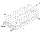
- FIG. 1 is an overall perspective view of a semiconductor electronic device with a lid removed;
- FIG. It is a figure explaining the conductor part on an insulating layer. It is a figure explaining the conductor part on an insulating layer. It is a figure explaining the conductor part on an insulating layer. It is a figure explaining the conductor part on an insulating layer. It is a figure explaining the conductor part on an insulating layer. It is a figure explaining the conductor part on an insulating layer. It is a figure explaining the conductor part on an insulating layer. It is a figure explaining the conductor part of the lower surface of an insulating layer. It is a figure which shows the side surface of a wiring laminated body. It is a perspective view which shows the modification 1 of a semiconductor package. It is a perspective view which shows the modification 2 of a semiconductor package.
- FIG. 1 is an overall perspective view of a semiconductor electronic device 1 of this embodiment with a lid 8 removed.
- the semiconductor electronic device 1 includes a semiconductor package 6, an electronic component 7, a lid 8, and the like.
- the semiconductor package 6 includes a substrate 10 (base portion), a wiring laminate 20 (wiring laminate portion), a wall 30 (peripheral wall portion), and the like.
- the semiconductor package 6 may have a fixture or the like used for fixing to an external substrate or the like.
- the substrate 10 has a top surface 11 (first surface) that is a surface on the +Z side, and along one side (first side; here, a side located on the +X side and extending in the Y direction) on the top surface 11, A wiring laminate 20 is located.
- the wiring laminate 20 and the wall 30 form a frame-like housing surrounding the upper surface 11 in a ring shape.
- the substrate 10 has a substantially rectangular shape (the corners may be rounded or may be cut off) when viewed from above in the Z direction, but the shape is not limited to this.
- the wiring laminate 20 has a plurality of insulating layers stacked in layers, and wiring conductors (first wiring conductors) such as a signal line, a ground line, and a power supply line are positioned on the upper surface of each insulating layer (at least two of them). is doing.
- the wiring laminate 20 includes a protruding portion 21a in which a part of the insulating layer that is continuous in the vertical direction (Z direction) protrudes outward (+X side) from the first side of the upper surface 11 (substrate 10) in plan view; It is divided into an inner portion 21b other than the projecting portion 21a located inside (-X side) of one side.
- Connection terminals located on the upper surface 211a (first upper surface) and the lower surface of the projecting portion 21a are connected to external wiring or the like.
- Two surfaces along the sides (second sides; here, two sides extending in the X direction) of the upper surface 11 connected to the first side are side surfaces 22 and 23 (second surfaces).
- An upper surface 24 (second upper surface) of the inner portion 21 b is partially joined to the wall 30 .
- a portion of the upper surface 24 is located outside (+X side) of the wall 30 .
- the conductor surface 24a (second conductor) may be located on the upper surface 24 .
- the conductor surface 24a is connected to a conductor 223 (first conductor) located at the boundary between the side surfaces 22 and 23 and the wall 30. As shown in FIG.
- the wall 30 is positioned along the outer edge of the substrate 10 in plan view and has an annular shape surrounding the upper surface 11 .
- the wall 30 is joined to the upper surface of the wiring laminate 20 in a portion overlapping the wiring laminate 20 in a plan view, and is joined to the substrate 10 in a portion not overlapping the wiring laminate 20 .
- the top surface of the wall 30 has a uniform height here, but is not limited to this.
- the semiconductor package 6 has an upper surface 11 of the substrate 10 as a bottom surface, and the upper surface 11 is surrounded by the wiring laminate 20 and the wall 30 to form a box-like shape having a recess opening upward.
- the wall body 30 has an opening 31 on one surface forming a side surface of the semiconductor package 6 and different from the side on which the wiring laminate 20 is located (the side of the first side of the upper surface 11). may Light can pass through this aperture 31, for example, if the electronic component 7 comprises an optical component such as a photodiode or a laser diode.
- the opening 31 may be partitioned between the inside and outside of the semiconductor package 6 by a light transmitting member such as glass or transparent resin.
- the wiring laminate 20 and the wall 30 are obtained by defining a three-dimensional shape and are obtained by, for example, mixing an organic binder and a solvent with material powder (for example, aluminum oxide and silicon oxide).
- material powder for example, aluminum oxide and silicon oxide.
- a plurality of insulating sheets (ceramic green sheets) formed by forming a slurry prepared by the method into a sheet shape are laminated, crimped and fired, and processed as necessary such as cutting and punching. you can In the production of the wiring laminate 20, for example, a metal paste is produced by mixing the above-described conductor metal, binder and organic solvent. Next, when the insulating sheets are laminated, the metal paste is applied to each insulating sheet by screen printing or the like.
- the wall body 30 may be a member different from the wiring laminated body 20, and may be, for example, a metal such as FeNiCo.
- the lid 8 is joined to the upper surface of the wall 30 and covers the upper surface of the recess.
- the wall 30 is a conductor, such as a metal including iron, copper, nickel, chromium, cobalt, molybdenum, or tungsten, or alloys thereof.
- the wiring laminate 20 has wiring conductors for transmitting signals and the like located on the upper surface (surface) of some or all of the plurality of insulating layers.
- the wiring conductors may include signal lines, ground lines, power supply lines, and the like.
- Each signal or power supply path (electrical path) by one or more wiring conductors connects the inside and the outside of the concave portion of the semiconductor package 6 .
- the electronic component 7 is positioned on the upper surface 11 of the substrate 10 and is housed inside the recess.
- One end of the electrical path inside the semiconductor package 6 and a terminal of the electronic component 7 are connected by a bonding wire or the like (not shown), and one end of the electrical path outside the semiconductor package 6 (the end opposite to the one end) is By connecting to an external board or the like via connection terminals (not shown), signal transmission/reception, power supply, and the like are performed.
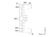
- Interlayer conductors 221 (first interlayer conductors) and interlayer conductors 222 (second interlayer conductors) for connecting wiring conductors on different insulating layers are positioned on the side surfaces 22 and 23 of the wiring laminate 20, as will be described later. .
- a conductor 223 (metallized layer; first conductor) is positioned along the outer edges of the side surfaces 22 and 23 that are in contact with the substrate 10 or the wall body 30 .
- the brazing material used for joining flows along the conductor 223 appropriately, so that the brazing material is excessively hardened on the joint surface. This is intended to prevent cracks or the like from occurring when stress is applied to the semiconductor package 6 by suppressing its remaining.
- FIGS. 2A to 5 are diagrams illustrating conductor portions on six insulating layers 201 to 206.
- FIG. FIG. 5 is a diagram for explaining the rear side of the lowermost insulating layer 206 among the six insulating layers 201 to 206. As shown in FIG. All of FIGS. 2A to 5 show the case when seen from the top side in planar see-through. Note that the number of insulating layers in the embodiment may be more than six layers.
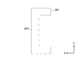
- FIG. 2A shows the uppermost insulating layer 201 .
- a conductive surface 2011 extends over the upper surface of the insulating layer 201 .
- a wall member 30 is joined onto the conductor surface 2011 via a brazing material or the like.
- FIG. 2B shows the insulating layer 202 which is the second layer from the top among the six layers.
- the insulating layer 202 includes lands 2021 to which the via-hole conductors in the via-holes penetrating the insulating layer 201 and the via-hole conductors in the via-holes penetrating the insulating layer 202 are connected, and signal lines 2022 extending from the lands 2021 to the side surfaces 22 and 23. and are located. That is, the signal line 2022 is electrically connected to the land 2034 (see FIG. 3A) through the via-hole conductor.
- lands 2021 and 2034 are shown here for explanation, the invention is not limited to this. Three or more lands 2021 and lands 2034 may be arranged in an appropriate positional relationship.
- the insulating layers 201 and 202 have a notch portion (depression) on the right side (-X side) of the figure.
- FIG. 3A shows the insulating layer 203 which is the third layer from the top among the six layers.
- a pair of signal lines 2032 and a pair of power supply lines 2033 and lands 2034 are shown.
- the depth (the width in the X direction) of the cutout portion of the insulating layer 203 is smaller than the cutout portions of the insulating layers 201 and 202, and the power supply line 2033 and the signal line 2032 located near the edges of the cutout portions. are exposed inside the notch portions of the insulating layers 201 and 202, respectively.
- the power supply line 2033 is connected to other ends located on the side surfaces 22 and 23, and the signal line 2032 is connected to the land 2034.
- the land 2034 overlaps with the land 2021 in plan perspective view, and these lands 2034 and 2021 are electrically connected via a via-hole conductor in the via-hole penetrating the insulating layer 202 .
- the vicinity of the exposed ends of the power supply line 2033 and signal line 2032 in the -X direction are connected to the electronic component 7 by bonding wires or the like inside the semiconductor package 6, and a predetermined voltage (ground voltage) is applied to the electronic component 7. including ).
- a predetermined voltage ground voltage
- a signal such as a DC signal or a signal switched at a low frequency (a low frequency is, as will be described later, a signal that does not require consideration of impedance matching).
- transmission lines (these are collectively referred to as wiring conductors).
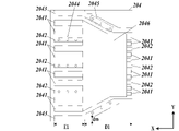
- FIG. 3B shows the insulating layer 204 which is the fourth layer from the top among the six layers.
- the left side (+X side) of the insulating layer 204 in the figure is the upper surface of the projecting portion 21 a and is exposed on the outer surface of the semiconductor package 6 .
- One end of the signal line 2041 and ground conductors 2042 and 2043 (ground conductors) are arranged in this exposed portion.
- two signal lines 2041 form a differential line
- ground conductors 2042 partially ground conductors 2043 are positioned on both sides ( ⁇ Y directions) of each set of differential lines.
- a connection terminal (lead terminal) not shown is joined to this one end of the signal line 2041, and the connection terminal is connected to an external signal line or the like.
- the signal line 2041 and the ground conductors 2042 and 2043 in FIG. 3B are enlarged for explanation, and their sizes, intervals and numbers are determined appropriately according to the number of signals, the size of the semiconductor package 6, and the like. can be
- the signal line 2041 and the ground conductor 2042 pass under the coating layer 2046 and are connected to the right side (-X side) of the drawing. Since the insulating layer 204 does not have a cutout portion, the right ( ⁇ X side) ends of the signal line 2041 and the ground conductors 2042 and 2043 are located inside the cutout portion of the insulating layer 203 and inside the semiconductor package 6 (recessed portion). ) side.
- the coating layer 2046 is, for example, an insulating thin film such as alumina.
- the right end of the signal line 2041 and the electronic component 7 are connected via a bonding wire (not shown) or the like, and signals are transmitted to and from the electronic component 7 .
- the signal to be transmitted is an RF signal, and may be a signal of 1 MHz or higher, especially in the GHz band.
- the ground conductors 2042 are in contact with the via-hole conductors 2044 respectively.
- a via-hole conductor 2044 is connected to a ground conductor surface 2051 on the insulating layer 205 through a via hole penetrating the insulating layer 204 .
- the insulating layer passes through a via hole that penetrates an insulating layer (not shown) located between the insulating layers 203 and 204.
- a via-hole conductor 2045 may be located that connects with the upper ground conductor plane.
- the ends of the ground conductors 2043 on both ends in the Y direction are exposed to the side surfaces 22 and 23 of the projecting portion 21a.
- This exposed portion E1 first region
- portions other than the exposed portion E1 adjacent portion D1 (second region) to the interlayer conductor 221) are located away from the side surfaces 22 and 23, respectively. 221 are located adjacent to each other.
- the edge (side) of the ground conductor 2043 extends in the direction along the first side (the direction perpendicular to the side surfaces 22 and 23) and extends between the adjacent portion D1 and the adjacent portion D1. It connects with the side surface 22 .
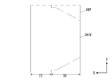
- FIG. 4A shows the fifth insulating layer 205 from the top of the six layers.
- a ground conductor surface 2051 (interlayer ground conductor) extends on the insulating layer 205 .
- the ground conductor surface 2051 straddles the exposed portion E2 and the adjacent portion D2 (that is, the range of the protruding portion 21a and the range other than the protruding portion 21a when viewed in plan view), and extends the range of the signal line 2041 on the insulating layer 204 when viewed in plan view. It extends to include everything.
- the ground conductor surface 2051 is exposed to the side surfaces 22 and 23 at the exposed portion E2, and separated from the side surfaces 22 and 23 at the adjacent portion D2 by a predetermined distance (distance dm).
- the sides bounding these regions extend along the first side (perpendicular to the sides 22, 23). The position of this side substantially overlaps the edge of the ground conductor 2042 between the exposed portion E1 and the adjacent portion D1 on the insulating layer 204 in FIG. 3B when seen from above.
- the wiring laminated body 20 is shaped by cutting, punching, etc. after fabrication. Physically, minute variations in the positions of the cutting and punching are unavoidable. vertical), even if some variation occurs, the position of the boundary in the X direction does not shift. Therefore, it is difficult for the exposed portions E1 and E2 to become wider or narrower than the necessary range, and in particular, the occurrence of unintended short circuits due to unnecessary exposed portions can be suppressed.
- FIG. 4B shows the bottom insulating layer 206 of the six layers.
- the lower surface (bottom surface) of the insulating layer 206 forms the lower surface of the projecting portion 21a.
- a signal line 2062 and a power supply line 2063 are located on the insulating layer 206 .
- the signal line 2062 has one end exposed to the side surfaces 22 and 23 and is in contact with one interlayer conductor 221 .
- One end opposite to the one end is connected to the via-hole conductor 2064, penetrates the insulating layer 206 through the via-hole conductor 2064, and is connected to the wiring conductor 2066 shown in FIG.
- the wiring conductor 2066 is exposed on the lower surface of the projecting portion 21a and is connected to an external wiring or the like via a connection terminal or the like.
- the power supply line 2063 has one end exposed to the side surfaces 22 and 23 and is in contact with the interlayer conductor 221 different from the one with which the signal line 2062 is in contact. One end opposite to the one end is connected to the via-hole conductor 2065, penetrates the insulating layer 206 through the via-hole conductor 2065, and is connected to the wiring conductor 2067 shown in FIG.
- the wiring conductor 2067 is exposed on the lower surface of the projecting portion 21a and is connected to an external wiring or the like via a connection terminal or the like.
- the interlayer conductor 221 includes planar interlayer conductors 221a and 221b positioned in a region surrounded by conductors 223 on the side surfaces of the inner portion 21b.
- An interlayer conductor 221a connects signal lines 2022 and 2062 of different insulating layers 202 and 206, respectively.
- An interlayer conductor 221b connects power supply lines 2033 and 2063 of different insulating layers 203 and 206, respectively.
- the interlayer conductors 221 may be located on the inner surfaces of the recesses each having a shape such as a semi-cylindrical shape.
- the interlayer conductor 222 is located outside (+X side) of the interlayer conductor 221, and the ground conductor 2043 of the different insulating layers 204 and 205 on the side surface of the projecting portion 21a (here, the ground conductor on the upper surface of the projecting portion 21a). ; first ground conductor) and the ground conductor surface 2051 are connected.
- the length of the interlayer conductor 222 in the X direction may be shorter than the length of the ground conductor 2043 in the X direction (length E1 in FIG. 3B).
- a portion of the electrical path can be exposed on the surface of the semiconductor package 6 for low-frequency AC signals that do not occur, eg, below 1 MHz.
- conventional power supply lines using via-hole conductors there is a limit to miniaturization due to the required lower limit distance (clearance) and positional restrictions between the surrounding signal lines in the insulating layer.
- the upper surface 24 of the inner portion 21b is the conductor surface 24a that connects with the conductor 223 as described above.
- FIG. 7A and 7B are perspective views showing modifications of the semiconductor package 6.
- FIG. FIG. 7A shows a semiconductor package 6a of Modification 1.
- FIG. in this semiconductor package 6a the wiring laminated body 20 and the wall body 30 form an integrated laminated body 20a.
- the laminated insulating layers each have a ring structure. This eliminates the need for the conductor 223 positioned along the joint surface with the wall 30 at the edge of the wiring laminate 20 . Since the structure of the portion (wiring laminated portion) corresponding to the other wiring laminated body 20 is the same as the structure of the above-described embodiment, the explanation thereof is omitted.
- FIG. 7B shows a semiconductor package 6b of Modification 2.
- the substrate 10, the wiring laminate 20, and the wall 30 are all integrated into a laminate 20b.
- the insulating layer in the portion corresponding to the substrate 10 is plate-shaped, and the insulating layer in the other portion is ring-shaped like the laminated body 20a. Since it is not a combination of multiple members, conductor 223 is not required.
- the ground conductor 2043a is not in contact with the side surfaces 22 and 23 in this modified example 2. Accordingly, the laminate 20b has an interlayer conductor 222 on the side surface. does not have Since other configurations and structures are the same as those of the above embodiment, description thereof is omitted. As described above, the wiring laminate 20 need not be an independent structure, and may be part of a laminate integrally formed with the wall 30 and/or the substrate 10 .
- the semiconductor package 6 of this embodiment includes the substrate 10 having the top surface 11 including the first side and the second side connected to the first side, and the first side of the top surface 11 on the top surface 11 . and a wiring laminate 20 having side surfaces 22 and 23 along the second side, and a wall 30 surrounding the upper surface 11 together with the wiring laminate 20 .
- the wiring laminate 20 includes a plurality of insulating layers 201 to 206 stacked in layers, and at least two signal lines 2022 and 2062 located on different insulating layers (202, 203, 206, etc.) in the plurality of insulating layers 201 to 206. and power supply lines 2033, 2063, and interlayer conductors 221 located on the side surfaces 22, 23 and connecting the at least two first wiring conductors.
- control signals, ground voltage, and power supply which are conventionally connected between different insulating layers through via holes, can be transmitted through the side surface of the semiconductor package.
- control signals, ground voltage, and power supply which are conventionally connected between different insulating layers through via holes, can be transmitted through the side surface of the semiconductor package.
- the interlayer conductors 221 are conductors that transmit low-frequency AC or DC signals such as power supplies. With such a signal, even if the electrical path is partially exposed outside the insulating layer, the impedance mismatch at the boundary where the exposure is switched does not matter, so the interlayer conductor 221 can be used without problems. can do.
- the electrical path including the interlayer conductor 221 may be a ground conductor. Also in this case, the electrical path may be exposed outside the insulating layer, and can appropriately connect between the ground conductors between the different insulating layers.
- the wiring laminate 20 may have two interlayer conductors 221a and 221b extending side by side on the side surfaces 22 and 23 . This makes it possible to transmit multiple types of signals and voltages in a small space.
- the wiring laminate 20 has recesses located in the side surfaces 22 and 23, and the interlayer conductors 221 may be conductors located within the recesses. Thereby, the area of the interlayer conductor 221 can be increased compared to the width in the X direction.
- the wiring laminate 20 includes a protruding portion 21a protruding outward from the first side and having an upper surface 211a, an inner portion 21b positioned inside ( ⁇ X side) of the first side, A ground conductor 2043 located on the upper surface 211a of the protruding portion 21a, a ground conductor surface 2051 extending across the protruding portion 21a and the inner portion 21b between the insulating layers, and a ground conductor 2043 and the ground conductor located on the side surfaces 22 and 23. and an interlayer conductor 222 connecting with the surface 2051 .
- a ground conductor between signal lines is arranged in the projecting portion 21a having a connection terminal of a signal line, and space tends to be insufficient due to miniaturization.
- the number of via holes can be reduced. An increase in size can be suppressed.
- the interlayer conductor 222 is located outside (+X side) of the interlayer conductor 221 on the side surfaces 22 and 23 . That is, by locating the interlayer conductor 222 connecting the conductors of the layer including the upper surface 211a of the projecting portion 21a to the conductors of other layers on the side of the projecting portion 21a, it is possible to efficiently arrange a plurality of interlayer conductors.
- the length in the X direction of the interlayer conductor 222 on the side surfaces 22 and 23 may be shorter than the length in the X direction of the ground conductor 2043 on the upper surface 211a. That is, as long as the interlayer conductor 222 has a width required, the ground conductor 2043 does not have to be in contact with the interlayer conductor 222 over the entire width, and there is no need to use conductor members more than necessary.
- At least one of the ground conductor 2043 and the ground conductor surface 2051 has an exposed portion E1 connected to the side surfaces 22 and 23 and a distance dm or more from the interlayer conductor 221 and the exposed portion E1 connected to the side surfaces 22 and 23 in plan view. It has an adjacent portion D1 and a side along the first side connecting the exposed portion E1 and the adjacent portion D1. That is, since the adjacent portion D1 is separated from the side surfaces 22 and 23, the adjacent portion D1 is not cut during manufacturing. In addition, since the edge of the portion connecting the adjacent portion D1 and the side surfaces 22 and 23 is perpendicular to the side surfaces 22 and 23 and is not inclined, the ground conductor 2043 and the ground conductor surface 2051 are connected even if the cutting position is deviated.
- the exposure range on the side surfaces 22, 23 of the is not changed.
- the interlayer conductors 221 and 222 are present on the side surfaces 22 and 23, the deviation of the exposed surfaces may lead not only to the deviation of the connection range but also to short circuits due to unintended connections with other parts. Therefore, by defining the range of the ground conductor in this way, it becomes possible to easily perform alignment without improving the accuracy of cutting during manufacturing, etc., and to obtain an appropriate electrical path. .
- the wiring laminate 20 also has conductors 223 positioned along the outer edges of the side surfaces 22 and 23 that are in contact with at least the substrate 10 or the wall 30 .
- the brazing material used for joining flows along the conductor 223 appropriately, thereby preventing the brazing material from being excessively solidified and remaining on the joining surface. , cracks or the like can be made less likely to occur when stress is applied to the semiconductor package 6 .
- the wiring laminate 20 has an upper surface 24 connected to the side surfaces 22 and 23 and a conductor surface 24a positioned on the upper surface 24, and the conductor surface 24a and the conductor 223 may be connected. .
- the wiring laminate 20 can be more stably grounded.
- the semiconductor electronic device 1 of this embodiment includes the semiconductor package 6 described above and the electronic component 7 positioned on the upper surface 11 of the substrate 10 . According to the semiconductor electronic device 1, the electric paths such as the ground line and the power supply line can be properly connected to allow the electronic component 7 to operate properly.
- the same interlayer conductors 221 and 222 are located at the same position on both the side surfaces 22 and 23 when seen from the same direction (the surface located between the side surfaces 22 and 23 is located at the same position). are positioned symmetrically), but the present invention is not limited to this.
- the side surfaces 22 and 23 may have different positions, numbers, sizes and shapes of interlayer conductors.
- interlayer conductors when multiple interlayer conductors are used for different purposes, such as ground lines, power supply lines, and signal lines for low-frequency signals, the positional relationship between the interlayer conductors should be adjusted. may be
- the semiconductor package 6 does not necessarily have the interlayer conductor 222 . If there is a space in projecting portion 21 a , interlayer connection may be made by a normal via-hole conductor without using interlayer conductor 222 .
- the interlayer conductor 221 is positioned so as to straddle the fourth insulating layer having the RF signal line, but the present invention is not limited to this. Interlayer conductors may connect between any different layers.
- the interlayer conductor is not limited to a rectangular shape extending in the Z direction. It may extend obliquely from the side surfaces 22 and 23, or may have a curved or broken line shape. Also, the thickness (the direction perpendicular to the Z direction) may not be uniform.
- the lid 8 is configured separately from the semiconductor package 6, but the semiconductor package 6 having the lid 8 may be used.
- the fabrication of the semiconductor package 6 is not limited to the one using the insulating sheet as described above. Other methods may be used.
- the semiconductor package 6 may not have the protruding portion 21a, and the protruding portion 21a may not be a protrusion of a part of the intermediate insulating layer.
- a top or bottom insulating layer may be included.
- the protruding portion 21a may not protrude over the entire length of the first side, and the protruding portion 21a may have a notch portion.
- the semiconductor package 6 may be manufactured and sold separately from the electronic component 7 .
- the lid 8 may be sold without being joined to the semiconductor package 6 .
- specific details such as the configurations, materials, and structures shown in the above embodiments can be changed as appropriate without departing from the gist of the present disclosure.
- the scope of the present invention includes the scope described in the claims and their equivalents.
- the present disclosure can be used for semiconductor packages and semiconductor electronic devices.
Landscapes
- Engineering & Computer Science (AREA)
- Microelectronics & Electronic Packaging (AREA)
- Production Of Multi-Layered Print Wiring Board (AREA)
- Physics & Mathematics (AREA)
- Geometry (AREA)
Priority Applications (3)
| Application Number | Priority Date | Filing Date | Title |
|---|---|---|---|
| US18/557,754 US20250079284A1 (en) | 2021-04-27 | 2022-04-26 | Semiconductor package and semiconductor electronic device |
| JP2023517559A JP7634657B2 (ja) | 2021-04-27 | 2022-04-26 | 半導体パッケージ及び半導体電子装置 |
| CN202280030874.4A CN117203755A (zh) | 2021-04-27 | 2022-04-26 | 半导体封装体以及半导体电子装置 |
Applications Claiming Priority (2)
| Application Number | Priority Date | Filing Date | Title |
|---|---|---|---|
| JP2021075421 | 2021-04-27 | ||
| JP2021-075421 | 2021-04-27 |
Publications (1)
| Publication Number | Publication Date |
|---|---|
| WO2022230883A1 true WO2022230883A1 (ja) | 2022-11-03 |
Family
ID=83848176
Family Applications (1)
| Application Number | Title | Priority Date | Filing Date |
|---|---|---|---|
| PCT/JP2022/018904 Ceased WO2022230883A1 (ja) | 2021-04-27 | 2022-04-26 | 半導体パッケージ及び半導体電子装置 |
Country Status (4)
| Country | Link |
|---|---|
| US (1) | US20250079284A1 (https=) |
| JP (1) | JP7634657B2 (https=) |
| CN (1) | CN117203755A (https=) |
| WO (1) | WO2022230883A1 (https=) |
Cited By (1)
| Publication number | Priority date | Publication date | Assignee | Title |
|---|---|---|---|---|
| WO2025070079A1 (ja) * | 2023-09-29 | 2025-04-03 | 京セラ株式会社 | 配線基板および電子モジュール |
Citations (4)
| Publication number | Priority date | Publication date | Assignee | Title |
|---|---|---|---|---|
| JP2006066867A (ja) * | 2004-02-26 | 2006-03-09 | Kyocera Corp | 電子部品収納用パッケージおよび電子装置 |
| JP2009010149A (ja) * | 2007-06-28 | 2009-01-15 | Kyocera Corp | 接続端子及びこれを用いたパッケージ並びに電子装置 |
| WO2009057691A1 (ja) * | 2007-10-30 | 2009-05-07 | Kyocera Corporation | 接続端子及びこれを用いたパッケージ並びに電子装置 |
| WO2014069123A1 (ja) * | 2012-10-30 | 2014-05-08 | 京セラ株式会社 | 電子部品収納用容器および電子装置 |
-
2022
- 2022-04-26 US US18/557,754 patent/US20250079284A1/en active Pending
- 2022-04-26 WO PCT/JP2022/018904 patent/WO2022230883A1/ja not_active Ceased
- 2022-04-26 CN CN202280030874.4A patent/CN117203755A/zh active Pending
- 2022-04-26 JP JP2023517559A patent/JP7634657B2/ja active Active
Patent Citations (4)
| Publication number | Priority date | Publication date | Assignee | Title |
|---|---|---|---|---|
| JP2006066867A (ja) * | 2004-02-26 | 2006-03-09 | Kyocera Corp | 電子部品収納用パッケージおよび電子装置 |
| JP2009010149A (ja) * | 2007-06-28 | 2009-01-15 | Kyocera Corp | 接続端子及びこれを用いたパッケージ並びに電子装置 |
| WO2009057691A1 (ja) * | 2007-10-30 | 2009-05-07 | Kyocera Corporation | 接続端子及びこれを用いたパッケージ並びに電子装置 |
| WO2014069123A1 (ja) * | 2012-10-30 | 2014-05-08 | 京セラ株式会社 | 電子部品収納用容器および電子装置 |
Cited By (1)
| Publication number | Priority date | Publication date | Assignee | Title |
|---|---|---|---|---|
| WO2025070079A1 (ja) * | 2023-09-29 | 2025-04-03 | 京セラ株式会社 | 配線基板および電子モジュール |
Also Published As
| Publication number | Publication date |
|---|---|
| CN117203755A (zh) | 2023-12-08 |
| JP7634657B2 (ja) | 2025-02-21 |
| US20250079284A1 (en) | 2025-03-06 |
| JPWO2022230883A1 (https=) | 2022-11-03 |
Similar Documents
| Publication | Publication Date | Title |
|---|---|---|
| EP3780259B1 (en) | Transition structure and multilayer transition structure for millimeter wave | |
| CN111699552B (zh) | 高频模块 | |
| US10806033B2 (en) | Interposer and electronic device | |
| US10512155B2 (en) | Wiring board, optical semiconductor element package, and optical semiconductor device | |
| JP7753391B2 (ja) | 配線基板、配線基板を用いた電子部品実装用パッケージ、および電子モジュール | |
| US11949144B2 (en) | Structure for mounting a transmission line substrate having interlayer connection conductors to another substrate by a conductive bonding material | |
| US20250151200A1 (en) | Wiring board, electronic component mounting package using wiring board, and electronic module | |
| JP7634657B2 (ja) | 半導体パッケージ及び半導体電子装置 | |
| JP2000236045A (ja) | 高周波パッケージ | |
| US20240074035A1 (en) | Wiring base and electronic device | |
| US20250351264A1 (en) | Wiring board, electronic component mounting package using wiring board, and electronic module | |
| JP7573040B2 (ja) | 配線基体および電子装置 | |
| US12328857B2 (en) | Electronic component module and method of manufacturing electronic component module | |
| JP7599007B2 (ja) | 電子部品実装用パッケージ及び電子装置 | |
| JP6856468B2 (ja) | 配線基板、電子部品用パッケージおよび電子装置 | |
| JP7432703B2 (ja) | 配線基体および電子装置 | |
| US20240063108A1 (en) | Semiconductor package and semiconductor electronic device | |
| CN113056092A (zh) | 布线基板 | |
| WO2021124805A1 (ja) | 電子部品モジュール | |
| JP6352839B2 (ja) | 高周波パッケージ | |
| JP7632744B2 (ja) | 高周波モジュール及び高周波モジュールの製造方法 | |
| JP6495701B2 (ja) | 電子部品収納用パッケージおよびその製造方法 | |
| US20240105600A1 (en) | Wiring substrate, wiring structure using wiring substrate, electronic component mounting package, and electronic module | |
| WO2024135849A1 (ja) | 配線基板、配線基板を用いた電子部品実装用基板、および電子モジュール | |
| JP5257763B2 (ja) | 多層回路基板 |
Legal Events
| Date | Code | Title | Description |
|---|---|---|---|
| 121 | Ep: the epo has been informed by wipo that ep was designated in this application |
Ref document number: 22795796 Country of ref document: EP Kind code of ref document: A1 |
|
| WWE | Wipo information: entry into national phase |
Ref document number: 202280030874.4 Country of ref document: CN |
|
| WWE | Wipo information: entry into national phase |
Ref document number: 2023517559 Country of ref document: JP |
|
| WWE | Wipo information: entry into national phase |
Ref document number: 18557754 Country of ref document: US |
|
| NENP | Non-entry into the national phase |
Ref country code: DE |
|
| 122 | Ep: pct application non-entry in european phase |
Ref document number: 22795796 Country of ref document: EP Kind code of ref document: A1 |
|
| WWP | Wipo information: published in national office |
Ref document number: 18557754 Country of ref document: US |