WO2022230288A1 - 弾性波装置 - Google Patents
弾性波装置 Download PDFInfo
- Publication number
- WO2022230288A1 WO2022230288A1 PCT/JP2022/004691 JP2022004691W WO2022230288A1 WO 2022230288 A1 WO2022230288 A1 WO 2022230288A1 JP 2022004691 W JP2022004691 W JP 2022004691W WO 2022230288 A1 WO2022230288 A1 WO 2022230288A1
- Authority
- WO
- WIPO (PCT)
- Prior art keywords
- layer
- main surface
- wave device
- elastic wave
- cavity
- Prior art date
- Legal status (The legal status is an assumption and is not a legal conclusion. Google has not performed a legal analysis and makes no representation as to the accuracy of the status listed.)
- Ceased
Links
Images






Classifications
-
- H—ELECTRICITY
- H03—ELECTRONIC CIRCUITRY
- H03H—IMPEDANCE NETWORKS, e.g. RESONANT CIRCUITS; RESONATORS
- H03H9/00—Networks comprising electromechanical or electro-acoustic elements; Electromechanical resonators
- H03H9/02—Details
- H03H9/02007—Details of bulk acoustic wave devices
- H03H9/02086—Means for compensation or elimination of undesirable effects
-
- H—ELECTRICITY
- H03—ELECTRONIC CIRCUITRY
- H03H—IMPEDANCE NETWORKS, e.g. RESONANT CIRCUITS; RESONATORS
- H03H9/00—Networks comprising electromechanical or electro-acoustic elements; Electromechanical resonators
- H03H9/15—Constructional features of resonators consisting of piezoelectric or electrostrictive material
- H03H9/17—Constructional features of resonators consisting of piezoelectric or electrostrictive material having a single resonator
-
- H—ELECTRICITY
- H03—ELECTRONIC CIRCUITRY
- H03H—IMPEDANCE NETWORKS, e.g. RESONANT CIRCUITS; RESONATORS
- H03H3/00—Apparatus or processes specially adapted for the manufacture of impedance networks, resonating circuits, resonators
- H03H3/007—Apparatus or processes specially adapted for the manufacture of impedance networks, resonating circuits, resonators for the manufacture of electromechanical resonators or networks
- H03H3/02—Apparatus or processes specially adapted for the manufacture of impedance networks, resonating circuits, resonators for the manufacture of electromechanical resonators or networks for the manufacture of piezoelectric or electrostrictive resonators or networks
-
- H—ELECTRICITY
- H03—ELECTRONIC CIRCUITRY
- H03H—IMPEDANCE NETWORKS, e.g. RESONANT CIRCUITS; RESONATORS
- H03H9/00—Networks comprising electromechanical or electro-acoustic elements; Electromechanical resonators
- H03H9/02—Details
- H03H9/125—Driving means, e.g. electrodes, coils
- H03H9/13—Driving means, e.g. electrodes, coils for networks consisting of piezoelectric or electrostrictive materials
- H03H9/131—Driving means, e.g. electrodes, coils for networks consisting of piezoelectric or electrostrictive materials consisting of a multilayered structure
-
- H—ELECTRICITY
- H03—ELECTRONIC CIRCUITRY
- H03H—IMPEDANCE NETWORKS, e.g. RESONANT CIRCUITS; RESONATORS
- H03H9/00—Networks comprising electromechanical or electro-acoustic elements; Electromechanical resonators
- H03H9/15—Constructional features of resonators consisting of piezoelectric or electrostrictive material
- H03H9/17—Constructional features of resonators consisting of piezoelectric or electrostrictive material having a single resonator
- H03H9/171—Constructional features of resonators consisting of piezoelectric or electrostrictive material having a single resonator implemented with thin-film techniques, i.e. of the film bulk acoustic resonator [FBAR] type
- H03H9/172—Means for mounting on a substrate, i.e. means constituting the material interface confining the waves to a volume
- H03H9/173—Air-gaps
-
- H—ELECTRICITY
- H03—ELECTRONIC CIRCUITRY
- H03H—IMPEDANCE NETWORKS, e.g. RESONANT CIRCUITS; RESONATORS
- H03H3/00—Apparatus or processes specially adapted for the manufacture of impedance networks, resonating circuits, resonators
- H03H3/007—Apparatus or processes specially adapted for the manufacture of impedance networks, resonating circuits, resonators for the manufacture of electromechanical resonators or networks
- H03H3/02—Apparatus or processes specially adapted for the manufacture of impedance networks, resonating circuits, resonators for the manufacture of electromechanical resonators or networks for the manufacture of piezoelectric or electrostrictive resonators or networks
- H03H2003/021—Apparatus or processes specially adapted for the manufacture of impedance networks, resonating circuits, resonators for the manufacture of electromechanical resonators or networks for the manufacture of piezoelectric or electrostrictive resonators or networks the resonators or networks being of the air-gap type
Definitions
- the present invention relates to an acoustic wave device having a structure in which a cavity is provided below a piezoelectric film.
- An object of the present invention is to provide an elastic wave device whose characteristics are less likely to deteriorate.
- An elastic wave device includes a first layer including a support substrate, provided on the first layer, a second layer including a piezoelectric film, and provided on the second layer. and an excitation electrode, wherein a cavity is provided between the first layer and the second layer, and the excitation electrode is arranged in the stacking direction of the first layer and the second layer. At least part of the electrode overlaps with the cavity, and the surface roughness of the main surface of the first layer facing the cavity is the same as that of the second layer facing the cavity. It is different from the surface roughness of the main surface.
- 1(a) and 1(b) are a plan view and a front cross-sectional view of an elastic wave device according to a first embodiment of the present invention.
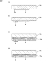
- 2(a) to 2(d) are front cross-sectional views for explaining the method of manufacturing the elastic wave device according to the first embodiment of the present invention.
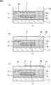
- 3(a) to 3(c) are front cross-sectional views for explaining the method of manufacturing the elastic wave device according to the first embodiment of the present invention.
- 4A to 4C are front cross-sectional views for explaining the method of manufacturing the elastic wave device according to the first embodiment of the present invention.
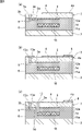
- 5(a) to 5(c) are front cross-sectional views for explaining the method of manufacturing the acoustic wave device according to the first embodiment of the present invention.
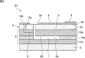
- FIG. 6 is a front cross-sectional view of an elastic wave device according to a second embodiment of the invention.
- 7(a) and 7(b) are schematic plan views showing a front cross-sectional view and an electrode structure of an elastic wave device according to a third embodiment of the present invention.
- FIG. 8 is a front cross-sectional view of an elastic wave device according to a fourth embodiment of the invention.
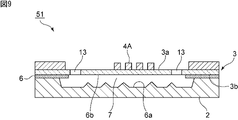
- FIG. 9 is a front cross-sectional view of an elastic wave device according to a fifth embodiment of the invention.
- 10(a) and 10(b) are a front cross-sectional view and a plan view of an elastic wave device according to a modification of the fifth embodiment.
- FIG. 11 is a front cross-sectional view of an acoustic wave device according to a sixth embodiment of the invention.
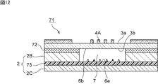
- FIG. 12 is a front cross-sectional view of an elastic wave device according to a seventh embodiment of the invention.
- 1(a) and 1(b) are a plan view of an elastic wave device according to a first embodiment of the present invention and a front cross-sectional view taken along line BB in FIG. 1(a).
- the second layer 12 including the piezoelectric film 3 is laminated on the first layer 11 including the support substrate 2 .
- the first excitation electrode 4, ie the top electrode is provided on the second layer 12.
- the support substrate 2 is made of silicon. However, the material forming the support substrate 2 is not particularly limited. Various insulating and semiconducting materials can be used.
- the piezoelectric film 3 is made of piezoelectric single crystal. Lithium tantalate, lithium niobate, crystal, or the like can be used as such a piezoelectric single crystal. In this embodiment, the piezoelectric film 3 is made of lithium tantalate. The piezoelectric film 3 only needs to contain a piezoelectric material, and does not necessarily need to be made of a piezoelectric single crystal.
- the piezoelectric film 3 has a first main surface 3a and a second main surface 3b located on the support substrate 2 side.
- a second excitation electrode 5, ie, a lower electrode is provided on the second main surface 3b.
- the first excitation electrode 4 and the second excitation electrode 5 have overlapping portions with the piezoelectric film 3 interposed therebetween. This overlapping portion becomes an excitation region.
- the first excitation electrode 4 has a lead portion 4a.
- the lead-out portion 4a is led out toward the edge 3d on the first main surface 3a.
- the width of the lead portion 4a is, for example, narrower than the width of the first excitation electrode 4 in the excitation region.
- a second layer wiring 8 is laminated on the lead portion 4a.
- the second excitation electrode 5 has a lead portion 5a.
- the lead-out portion 5a extends from the excitation region toward the edge 3c.
- the edge 3c is an edge opposite to the edge 3d.
- the width of the lead-out portion 5a is narrower than the width of the second excitation electrode 5 in the excitation region.
- a through hole 13, which will be described later, is positioned in the middle of the drawer portion 5a.
- a second layer wiring 9 is laminated on the lead portion 5a.
- a through-hole electrode 10a passing through the piezoelectric film 3 is connected to the lead portion 5a.
- a terminal electrode 10b is provided on the first main surface 3a so as to be connected to the through-hole electrode 10a.
- An AC voltage can be applied from the outside by the second layer wiring 8 and the terminal electrode 10b. Thereby, the excitation region is excited in the piezoelectric film 3 .
- the first and second excitation electrodes 4 and 5, the second layer wirings 8 and 9, the through-hole electrodes 10a and the terminal electrodes 10b are made of appropriate metals or alloys. Such materials include Al, Pt, Cu, W, Mo, or alloys containing these metals. Also, these electrodes and wiring may be composed of a laminate of a plurality of metal films.
- the intermediate layer 6 is provided between the support substrate 2 and the piezoelectric film 3 .
- the intermediate layer 6 can be made of an appropriate insulating material. Silicon oxide, silicon oxynitride, alumina, or the like can be used as such an insulating material. In this embodiment, the intermediate layer 6 is made of silicon oxide.
- a hollow portion 7 is provided in the intermediate layer 6 .
- the cavity 7 is provided so as to overlap the first excitation electrode 4 in the stacking direction of the first layer 11 and the second layer 12, as shown in FIG. 1(b).
- the rectangular first excitation electrode 4 it is preferable that the rectangular first excitation electrode 4 entirely overlaps the hollow portion 7 indicated by the dashed-dotted line. If the entire first excitation electrode 4 and lead-out portion 4a are considered to be the excitation electrode, part of the excitation electrode may overlap the hollow portion 7 .
- a through hole 13 is connected to the hollow portion 7 .
- the through-hole 13 extends from the first main surface 3 a of the piezoelectric film 3 toward the first layer 11 side and reaches the hollow portion 7 . Note that the through hole 13 may not be provided.
- the through hole 13 may or may not penetrate the drawer portion 5a.
- the through hole 13 may be provided in a region where the lead portion 5a is not provided.
- the through-hole 13 acts on excitation, and can improve the confinement efficiency of waves and spurious.
- the intermediate layer 6 includes a first intermediate layer 11a forming part of the first layer 11, a second intermediate layer 12a forming part of the second layer 12, and a first It has an intermediate layer 11a and a third intermediate layer 14 positioned between the second intermediate layer 12a.
- a cavity 7 is provided in the third intermediate layer 14 . Therefore, the cavity 7 is provided between the first layer 11 and the second layer 12 .
- the first intermediate layer 11a is provided on the main surface 6a of the support substrate 2 on the side of the cavity 7.
- the second intermediate layer 12a is provided on the main surface 3b of the piezoelectric film 3 on the cavity 7 side.
- the first intermediate layer 11a, the second intermediate layer 12a, and the third intermediate layer 14 are integrally formed of silicon oxide.
- the first to third intermediate layers 11a, 12a, 14 may be made of the same material or may be made of different materials.
- the surface roughness Ra of the main surface 6a of the first layer 11 facing the cavity 7 is made larger than the surface roughness Ra of the main surface 6b of the second layer 12 facing the cavity 7. ing.
- the surface roughness Ra is the arithmetic mean roughness Ra specified in JIS B0601.
- the value of the surface roughness Ra of the main surface 6a is made larger than the value of the surface roughness Ra of the main surface 6b.
- the surface roughness Ra can be calculated by surface morphology measurement using SPM (Scanning Probe Microscope) or SEM (Scanning Electron Microscope).
- the surface roughness Ra of the first main surface 6a may be different from the surface roughness Ra of the second main surface 6b.
- the main surface 6b may be a smooth surface instead of a rough surface. good too.
- both the main surface 6a and the main surface 6b have the surface roughness Ra of the main surface of the second layer 12 on which the first excitation electrode 4 is provided. It is larger than the surface roughness Ra of the first main surface 3a. In that case, as will be described later, unwanted waves can be scattered more effectively, and deterioration of characteristics is less likely to occur.
- the surface roughness Ra of the main surface 6a is larger than the surface roughness Ra of the main surface 6b. Therefore, unwanted waves can be effectively scattered. Thereby, deterioration of the characteristics of the elastic wave device 1 can be suppressed.
- the surface roughness Ra of the main surfaces 6a and 6b is 0.5 nm or more. More preferably, the surface roughness Ra of the main surfaces 6a and 6b is 1 nm or more. Thereby, unwanted waves can be suppressed more effectively.
- the upper limit of the surface roughness Ra is set so as not to exceed the film thickness of the first intermediate layer 11a and the second intermediate layer 12a. Otherwise, the support substrate 2 and the second excitation electrodes 5 may be damaged.
- both the principal surfaces 6 a and 6 b are principal surfaces of the intermediate layer 6 , but the principal surface 6 b may be the principal surface of the piezoelectric film 3 and the principal surface 6 a may be the principal surface of the support substrate 2 .
- the main surface 6 b is the main surface of the intermediate layer 6
- the chemical solution used during the process of manufacturing the elastic wave device 1 is applied to the piezoelectric film 3 .
- the piezoelectric film 3 and the supporting substrate 2 are more likely to be separated from each other. The effect of eliminating the need for alignment when bonding the substrates 2 is likely to be achieved.
- the method of roughening the main surfaces 6a and 6b is not particularly limited. Etching methods such as reactive ion etching (RIE) and dry etching, polishing with laser, and the like can be used.
- RIE reactive ion etching
- dry etching polishing with laser, and the like
- a second excitation electrode 5 and lead portions 5a are formed on one surface of a piezoelectric substrate 3A made of a piezoelectric single crystal.
- the second layer wiring 9 is formed on the lead portion 5a.
- the method of forming the second excitation electrode 5 and the second layer wiring 9 is not particularly limited, they can be formed by a lift-off method or the like using photolithography. Also, the second excitation electrode 5 and the lead-out portion 5a may be formed by sputtering or the like.
- the second intermediate layer 12a is formed by depositing silicon oxide. Protruding portions of the second intermediate layer 12a overlapping the second excitation electrode 5 and the second layer wiring 9 are removed by etching, polishing, or the like. In this manner, the lower surface of the second intermediate layer 12a is flattened and roughened as shown in FIG. 2(d). By controlling the etching conditions, it is possible to control the surface roughness of the lower surface of the second intermediate layer 12a, that is, the main surface 6b, which will be described later.
- a sacrificial layer 15 is laminated on the lower surface of the second intermediate layer 12a.
- the sacrificial layer 15 is made of a material that can be removed by an etchant, which will be described later. Although such a material is not particularly limited, it is made of ZnO in this embodiment.
- the sacrificial layer 15 can be formed by an appropriate thin film formation method such as sputtering.
- a sacrificial layer 15 is provided as shown in FIG. Next, the lower surface of the sacrificial layer 15 is roughened by etching or the like. By controlling the etching conditions, the surface roughness of the lower surface of the sacrificial layer 15 can be made different from the surface roughness of the upper surface of the sacrificial layer 15, that is, the lower surface of the second intermediate layer 12a.
- a film of silicon oxide is further continuously formed.
- the intermediate layer 6 is thereby formed. Therefore, the third intermediate layer 14 and the first intermediate layer 11a are laminated integrally with the second intermediate layer 12a.
- the silicon oxide film protrudes downward by the thickness of the sacrificial layer 15 .
- the projecting portion is removed and flattened. This planarization can be performed by etching, CMP polishing, or the like.
- the surface roughness of the lower surface of the sacrificial layer 15 is made larger than the surface roughness of the upper surface.
- the surface roughness of the lower surface of the sacrificial layer 15 finally corresponds to the surface roughness of the main surface 6a facing the cavity 7.
- the surface roughness of the upper surface of the sacrificial layer 15 corresponds to the surface roughness of the main surface 6b.
- the support substrate 2 is bonded to the intermediate layer 6 as shown in FIG. 4(a).
- the piezoelectric substrate 3A is ground using CMP polishing or a grinder. As a result, a thin piezoelectric film 3 is formed as shown in FIG. 4(b).
- the first excitation electrode 4 and the lead portion 4a are provided.
- the first excitation electrode 4 and the lead-out portion 4a can be formed in the same manner as the method for forming the second excitation electrode 5 and the like.
- a through hole 3e is provided in the piezoelectric film 3 as shown in FIG. 5(a). After that, as shown in FIG. 5B, a through-hole electrode 10a is formed to fill the through-hole 3e, and a terminal electrode 10b is formed. Also, a second layer wiring 8 is formed.
- an etchant for removing the sacrificial layer 15 from the through hole 13 is injected. Then, the material forming the sacrificial layer 15 is dissolved and removed. In this manner, the elastic wave device 1 shown in FIG. 1(b) can be obtained.
- the surface roughness of the main surface 6a is larger than the surface roughness of the main surface 6b, the time required for removing the sacrificial layer 15 with the etching solution is shortened. It's easy to do. Therefore, the damage caused by the etchant to the main surface 6b is reduced, and the effect of being able to suppress the characteristic deterioration is also exhibited.
- FIG. 6 is a front cross-sectional view of an elastic wave device according to a second embodiment of the invention.
- the material forming the third intermediate layer 14A is different from the material forming the first intermediate layer 11a and the second intermediate layer 12a. That is, a third intermediate layer 14A made of a different material is provided between the first intermediate layer 11a and the second intermediate layer 12a.
- the materials of the first intermediate layer 11a, the second intermediate layer 12a, and the third intermediate layer 14A may be different.
- the first intermediate layer 11a and the second intermediate layer 12a may be made of different materials.
- the surface roughness of the main surfaces 6a and 6b facing the hollow portion 7 is the same as that of the elastic wave device 1. Therefore, unnecessary waves can be scattered, and deterioration of characteristics can be suppressed.
- FIG. 7(a) and 7(b) are schematic plan views showing a front cross-sectional view and an electrode structure of an acoustic wave device according to a third embodiment of the present invention.
- the first excitation electrode 4A is provided on the piezoelectric film 3.
- the first excitation electrode 4A is an IDT electrode having a first comb-teeth electrode 4A1 and a second comb-teeth electrode 4A2.
- the first comb-teeth electrode 4A1 has a first bus bar 4A1a and a plurality of first electrode fingers 4A1b having base ends connected to the first bus bar 4A1a.
- the second comb-shaped electrode 4A2 has a second bus bar 4A2a facing the first bus bar 4A1a, and a plurality of second electrode fingers 4A2b having base ends connected to the second bus bar 4A2a. is doing.
- the plurality of first electrode fingers 4A1b and the plurality of second electrode fingers 4A2b are interposed with each other.
- the excitation electrodes provided on the piezoelectric film 3 may be IDT electrodes.
- the surface roughness of the main surfaces 6a and 6b facing the hollow portion 7 is the same as that of the elastic wave device 1 of the first embodiment. Therefore, it is possible to scatter unwanted waves and effectively suppress deterioration of characteristics.
- FIG. 8 is a front cross-sectional view of an elastic wave device according to a fourth embodiment of the invention.
- the surface roughnesses of the main surfaces 6a and 6b facing the cavity 7 are different from each other. Therefore, it is possible to scatter unwanted waves and effectively suppress deterioration of characteristics.
- the main surface 6a is provided with a plurality of protrusions that protrude from the main surface 6a toward the hollow portion 7 .
- the plurality of projections provided on the main surface 6a include projections having different heights (sizes in the stacking direction of the support substrate 2 and the piezoelectric film 3). This makes it easier to prevent the piezoelectric film 3 from bending toward the cavity 7 and sticking to the main surface 6a.
- the plurality of projections provided on the main surface 6a have a tapered shape in which the width becomes narrower toward the hollow portion 7 side. Specifically, when viewed from above in the stacking direction of the support substrate 2 and the piezoelectric film 3, the plurality of convex portions are arranged in dots. The plurality of projections provided on the main surface 6a have sharp ends on the hollow portion 7 side. In other words, even if the piezoelectric film 3 bends and sticks to the main surface 6a, the vibration of the piezoelectric film 3 is less likely to be disturbed, and the characteristic deterioration of the acoustic wave device 41 can be suppressed.
- the total area of the overlapping area of the ends of the plurality of convex portions on the side of the hollow portion 7 and the piezoelectric film 3 is equal to the area of the support substrate 2 and the piezoelectric film 3. It may be less than 5% of the area of the piezoelectric film 3 that overlaps with the cavity 7 when viewed in plan in the stacking direction with the film 3 . In this case, it becomes easier to suppress deterioration of the characteristics of the elastic wave device 41 more reliably.
- FIG. 9 is a front cross-sectional view of an elastic wave device according to a fifth embodiment of the invention.
- the surface roughnesses of the main surfaces 6a and 6b facing the cavity 7 are different from each other. Therefore, it is possible to scatter unwanted waves and effectively suppress deterioration of characteristics.
- adjacent convex portions among the plurality of convex portions provided on the main surface 6a may be provided with a predetermined distance therebetween. This makes it easier to prevent the piezoelectric film 3 from bending toward the cavity 7 and sticking to the main surface 6a.
- the flexible portions of the piezoelectric film 3 and the regions between the adjacent convex portions are provided so as to overlap each other in a plan view in the stacking direction of the support substrate 2 and the piezoelectric film 3 .
- the piezoelectric film 3 is less likely to stick to the main surface 6a of the support substrate 2 even when the piezoelectric film 3 is bent.
- the portion of the piezoelectric film 3 that is likely to bend is sandwiched between the projections when viewed from above in the lamination direction of the support substrate 2 and the piezoelectric film 3 . Therefore, the piezoelectric film 3 becomes more difficult to bend.
- a convex portion is not provided in a portion that overlaps the intersection region of the IDT electrode 52 (the region where the first and second electrode fingers of the IDT electrode 52 overlap each other when viewed in the direction in which the electrode fingers are arranged), and a portion that does not overlap the intersection region is provided. may be provided with a convex portion.
- a portion of the piezoelectric film 3 that overlaps the intersection region when viewed from above in the stacking direction of the support substrate 2 and the piezoelectric film 3 is more likely to bend than other portions. Therefore, by not providing the protrusions in the portions overlapping with the intersection regions and providing the protrusions in the other portions, it becomes easier to suppress sticking of the piezoelectric film 3 to the main surface 6a.
- FIG. 11 is a front cross-sectional view of an elastic wave device according to a sixth embodiment of the invention.
- the main surfaces 6a and 6b facing the cavity 7 have different surface roughnesses Ra.
- the surface roughness Ra of the main surface 6a is rougher than the surface roughness Ra of the main surface 6b.
- an intermediate layer 62 is provided between the supporting substrate 2A and the piezoelectric film 3.
- the intermediate layer 62 is provided with a recess opening toward the piezoelectric film 3 , thereby forming a cavity 7 .
- the main surface 6 a is the main surface of the material forming the intermediate layer 62 facing the hollow portion 7 .
- the principal surface 6 b is the principal surface facing the hollow portion 7 of the piezoelectric film 3 , that is, the second principal surface 3 b of the piezoelectric film 3 . Therefore, as in the first embodiment, the portion between the main surface 62b of the intermediate layer 62 on the support substrate 2A side and the main surface 6a corresponding to the lower surface of the cavity 7 becomes the first intermediate layer 11a.
- a portion between the main surface 62 a of the intermediate layer 62 on the side of the piezoelectric film 3 and the main surface 6 a that is the lower surface of the hollow portion 7 is the third intermediate layer 14 .
- the material of the intermediate layer 62 is not particularly limited, a bonding material made of an inorganic material, a synthetic resin, or the like can be used as in the above-described embodiments.
- FIG. 12 is a front cross-sectional view of an elastic wave device according to a seventh embodiment of the invention.
- the second support substrate layer 2B is laminated on the third support substrate layer 2C with the support substrate intermediate layer 73 interposed therebetween.
- An intermediate layer 72 is provided between the support substrate 2 and the piezoelectric film 3 .
- the cavity 7 is provided so as to penetrate the intermediate layer 72 and the second support substrate layer 2B. Therefore, the main surface 6 a facing the cavity 7 is the upper surface of the support substrate intermediate layer 73 .
- the main surface 6b facing the cavity 7 is the second main surface 3b of the piezoelectric film 3. As shown in FIG.
- the surface roughness Ra of the main surface 6a and the surface roughness Ra of the main surface 6b are different. More specifically, the surface roughness Ra of the main surface 6a is larger than the surface roughness Ra of the main surface 6b.
- the support substrate 2 may have a structure in which the second support substrate layer 2B is laminated on the third support substrate layer 2C with the support substrate intermediate layer 73 interposed therebetween.
- the support substrate intermediate layer 73 is made of an appropriate material such as a synthetic resin or an inorganic material.
Landscapes
- Physics & Mathematics (AREA)
- Acoustics & Sound (AREA)
- Engineering & Computer Science (AREA)
- Manufacturing & Machinery (AREA)
- Surface Acoustic Wave Elements And Circuit Networks Thereof (AREA)
Abstract
特性の劣化が生じ難い、弾性波装置を提供する。 支持基板2を含む第1の層11と、第1の層11上に設けられており、圧電膜3を含む第2の層12と、第2の層12上に設けられた励振電極4と、備え、第1の層11と第2の層12との間に空洞部7が設けられており、第1の層11と第2の層12との積層方向において、励振電極4の少なくとも一部が空洞部7と重なっており、空洞部7に面している第1の層11の主面6aの表面粗さが、空洞部7に面している第2の層12の主面6bの表面粗さと異なっている、弾性波装置1。
Description
本発明は、圧電膜の下方に空洞部が設けられている構造を有する弾性波装置に関する。
従来、圧電膜の下方に空洞部が設けられている弾性波装置が知られている。例えば下記の特許文献1では、圧電膜の上面及び下面に駆動電極が設けられている。そして、この圧電膜の下方に空洞部が設けられている。それによって、メンブレン構造を有する弾性波装置が構成されている。
圧電膜の下方に空洞部が設けられているメンブレン構造を有する弾性波装置では、不要波の励振による特性の劣化が生じることがあった。
本発明の目的は、特性の劣化が生じ難い、弾性波装置を提供する。
本発明に係る弾性波装置は、支持基板を含む第1の層と、前記第1の層上に設けられており、圧電膜を含む第2の層と、前記第2の層上に設けられた励振電極と、を備え、前記第1の層と前記第2の層との間に空洞部が設けられており、前記第1の層と前記第2の層との積層方向において、前記励振電極の少なくとも一部が前記空洞部と重なっており、前記空洞部に面している前記第1の層の主面の表面粗さが、前記空洞部に面している前記第2の層の主面の表面粗さと異なっている。
本発明によれば、特性の劣化が生じ難い、弾性波装置を提供することができる。
以下、図面を参照しつつ、本発明の具体的な実施形態を説明することにより、本発明を明らかにする。
なお、本明細書に記載の各実施形態は、例示的なものであり、異なる実施形態間において、構成の部分的な置換または組み合わせが可能であることを指摘しておく。
図1(a)及び図1(b)は、本発明の第1の実施形態に係る弾性波装置の平面図及び図1(a)中のB-B線に沿う正面断面図である。
弾性波装置1では、支持基板2を含む第1の層11上に、圧電膜3を含む第2の層12が積層されている。第2の層12上に、第1の励振電極4、すなわち上部電極が設けられている。
支持基板2は、シリコンからなる。もっとも、支持基板2を構成する材料は特に限定されない。様々な絶縁性材料や半導体材料を用いることができる。
圧電膜3は、圧電単結晶からなる。このような圧電単結晶としては、タンタル酸リチウム、ニオブ酸リチウムまたは水晶などを用いることができる。本実施形態では、圧電膜3は、タンタル酸リチウムからなる。なお、圧電膜3は、圧電性の材料を含んでいればよく、必ずしも圧電単結晶からなる必要性はない。
圧電膜3は、第1の主面3aと、支持基板2側に位置している第2の主面3bとを有する。第2の主面3bに、第2の励振電極5、すなわち下部電極が設けられている。第1の励振電極4と第2の励振電極5とは、圧電膜3を介して重なり合っている部分を有する。この重なり合っている部分が、励振領域となる。
第1の励振電極4は、引き出し部4aを有する。引き出し部4aは、第1の主面3a上において、端縁3dに向かって引き出されている。この引き出し部4aの幅は、例えば、励振領域における第1の励振電極4の幅より細くされている。そして、引き出し部4a上に、2層目配線8が積層されている。
第2の励振電極5は、引き出し部5aを有する。引き出し部5aは、励振領域から、端縁3c側に向かって延ばされている。端縁3cは、端縁3dとは反対側の端縁である。
引き出し部5aの幅は、励振領域における第2の励振電極5の幅よりも細くされている。引き出し部5aの途中には、後述する貫通孔13が位置している。引き出し部5aに、2層目配線9が積層されている。
上記引き出し部5aに、圧電膜3を貫通しているスルーホール電極10aが接続されている。スルーホール電極10aに接続されるように、第1の主面3a上に、端子電極10bが設けられている。2層目配線8と、端子電極10bとにより、外部から交流電圧を印加することができる。それによって、圧電膜3において、励振領域が励振される。
上記第1,第2の励振電極4,5、2層目配線8,9、スルーホール電極10a及び端子電極10bは、適宜の金属もしくは合金からなる。このような材料としては、Al、Pt、Cu、W、Moまたはこれらの金属を含む合金などが挙げられる。また、これらの電極や配線は、複数の金属膜の積層体からなるものであってもよい。
支持基板2と、圧電膜3との間には、中間層6が設けられている。中間層6は、適宜の絶縁性材料により形成することができる。このような絶縁性材料としては、酸化ケイ素、酸窒化ケイ素、アルミナなどを用いることができる。本実施形態では、中間層6は、酸化ケイ素からなる。
中間層6には、空洞部7が設けられている。空洞部7は、図1(b)に示すように、第1の層11及び第2の層12の積層方向において、第1の励振電極4と重なるように設けられている。なお、図1(a)に示すように、一点鎖線で示す空洞部7上に、矩形の第1の励振電極4の全体が重なっていることが好ましい。第1の励振電極4と引き出し部4aの全体を励振電極と考えた場合には、励振電極の一部が空洞部7に重なっておればよい。
空洞部7には、貫通孔13が連なっている。貫通孔13は、圧電膜3の第1の主面3aから第1の層11側に向かって延び、空洞部7に至っている。なお、貫通孔13は設けられていなくてもよい。
この貫通孔13は、前述したように、引き出し部5aを貫いていても良いし、貫いていなくても良い。言い換えれば、引き出し部5aが設けられていない領域に貫通孔13が設けられていても良い。なお、貫通孔13が引き出し部5aを貫く場合は、励振に作用し、波の閉じ込め効率や、スプリアスを改善できる。
中間層6は、第1の層11の一部を構成している第1の中間層11aと、第2の層12の一部を構成している第2の中間層12aと、第1の中間層11aと、第2の中間層12aとの間に位置している第3の中間層14とを有する。第3の中間層14において、空洞部7が設けられている。従って、空洞部7は、第1の層11と、第2の層12との間に設けられていることになる。また、第1の中間層11aは、支持基板2の空洞部7側の主面6a上に設けられている。第2の中間層12aは、圧電膜3の空洞部7側の主面3bに設けられている。
本実施形態では、第1の中間層11a、第2の中間層12a及び第3の中間層14が、酸化ケイ素により一体に構成されている。なお、第1~第3の中間層11a,12a,14は、同じ材料で形成されていてもよく、異なる材料で形成されていてもよい。空洞部7に面している第1の層11の主面6aの表面粗さRaは、空洞部7に面している第2の層12の主面6bの表面粗さRaよりも大きくされている。ここで、表面粗さRaとは、JIS B0601に規定されている算術平均粗さRaである。本実施形態では、主面6aの表面粗さRaの値が、主面6bにおける表面粗さRaの値よりも大きくされている。なお、表面粗さRaは、SPM(Scanning Probe Microscope)やSEM(Scanning Eletron Microscope)などを使用した表面モフォロジー測定で算出できる。
なお、第1の主面6aの表面粗さRaは、第2の主面6bの表面粗さRaと異なっていればよく、例えば、主面6bは、粗面でなく平滑な面であってもよい。
好ましくは、本実施形態のように、主面6a及び主面6bの表面粗さRaが、いずれも、第2の層12の第1の励振電極4が設けられている側の主面である第1の主面3aの表面粗さRaよりも大きい。その場合には、後述するように、不要波をより効果的に散乱させることができ、特性の劣化が生じ難い。
弾性波装置1では、主面6aの表面粗さRaが主面6bの表面粗さRaよりも大きい。そのため、不要波を効果的に散乱させることができる。それによって、弾性波装置1の特性の劣化を抑制することができる。
好ましくは、主面6a及び主面6bの表面粗さRaは、0.5nm以上とされる。さらに好ましくは、主面6a及び主面6bの表面粗さRaは、1nm以上とされる。それによって、不要波をより効果的に抑制することができる。なお、表面粗さRaの上限は、第1の中間層11aや第2の中間層12aの膜厚を超えない程度とされる。さもないと、支持基板2や第2の励振電極5が損傷するおそれがある。
なお、弾性波装置1では主面6a,主面6bはいずれも中間層6の主面であるが、主面6bは圧電膜3の主面でもよく、主面6aは支持基板2の主面であってもよい。主面6bが中間層6の主面である場合には、主面6bが圧電膜3の主面である場合に比べて、弾性波装置1を製造するプロセス中に用いる薬液による圧電膜3へのダメージを低減できるという効果が奏されやすい。また、主面6aが中間層6の主面である場合には、主面6aが支持基板2の主面である場合に比べて、弾性波装置1を製造するプロセスにおいて、圧電膜3と支持基板2を接合する際にアライメントが不要になるという効果が奏されやすい。
主面6a,6bを粗面とする方法は特に限定されない。反応性イオンエッチング(RIE)、ドライエッチングなどのエッチング方法やレーザーによる研磨などを用いることができる。
次に、弾性波装置1の製造方法を、図2(a)~図2(d)、図3(a)~図3(c)、図4(a)~図4(c)及び図5(a)~図5(c)を参照して説明する。
図2(a)に示すように、圧電単結晶からなる圧電基板3Aの一方面に第2の励振電極5及び引き出し部5aを形成する。次に、2層目配線9を引き出し部5a上に形成する。この第2の励振電極5及び2層目配線9の形成方法は特に限定されないが、フォトリソグラフィを用いてリフトオフ法などにより形成することができる。また、第2の励振電極5及び引き出し部5aは、スパッタリングなどにより形成されてもよい。
次に、図2(c)に示すように、酸化ケイ素を成膜することにより、第2の中間層12aを形成する。第2の中間層12aの第2の励振電極5及び2層目配線9に重なり合っている部分における突出部をエッチングや研磨などにより除去する。このようにして、図2(d)に示すように、第2の中間層12aの下面を平坦化すると共に、下面を粗面にする。エッチングに際しての条件を制御することにより、第2の中間層12aの下面、すなわち後述する主面6bの表面粗さをコントロールすることができる。
次に、図3(a)に示すように、犠牲層15を第2の中間層12aの下面に積層する。犠牲層15は、後述のエッチャントにより除去し得る材料からなる。このような材料としては特に限定されないが、本実施形態では、ZnOからなる。犠牲層15は、スパッタリングなどの適宜の薄膜形成方法により形成することができる。
図3(a)に示すように、犠牲層15を設ける。次に、犠牲層15の下面をエッチングなどにより粗面とする。このエッチングの条件をコントロールすることにより、犠牲層15の下面の表面粗さと、犠牲層15の上面すなわち第2の中間層12aの下面の表面粗さを異ならせることができる。
次に、図3(b)に示すように、酸化ケイ素をさらに連続的に成膜する。それによって、中間層6を形成する。よって、第2の中間層12aに一体に、第3の中間層14及び第1の中間層11aが積層されることになる。なお、犠牲層15が設けられていた部分の下方では、酸化ケイ素膜が犠牲層15の厚みの分だけ下方に突出している。図3(c)に示すように、上記突出している部分を除去し平坦化する。この平坦化は、エッチングやCMP研磨などにより行い得る。
本実施形態では、図3(b)に示すように、犠牲層15の下面の表面粗さが、上面の表面粗さよりも大きくされている。この犠牲層15の下面の表面粗さが、最終的に空洞部7に臨む主面6aの表面粗さに対応する。また、犠牲層15の上面の表面粗さが、主面6bの表面粗さに対応することとなる。
次に、図4(a)に示すように、支持基板2を中間層6に接合する。
次に、圧電基板3AをCMP研磨やグラインダーを用いて研削する。それによって、図4(b)に示すように、厚みの薄い圧電膜3を形成する。
次に、図4(c)に示すように、第1の励振電極4及び引き出し部4aを設ける。この第1の励振電極4及び引き出し部4aは、第2の励振電極5などの形成方法と同様にして形成することができる。
図5(a)に示すように、スルーホール3eを圧電膜3に設ける。しかる後、図5(b)に示すように、スルーホール3eを埋めるように、スルーホール電極10aを形成し、さらに端子電極10bを形成する。また、2層目配線8を形成する。
次に、図5(c)に示すように、貫通孔13を設ける。
次に、貫通孔13から犠牲層15を除去するためのエッチング液を注入する。そして、犠牲層15を構成している材料を溶解し、除去する。このようにして、図1(b)に示した弾性波装置1を得ることができる。
なお、第1の実施形態に係る弾性波装置1においては、主面6aの表面粗さが主面6bの表面粗さよりも大きいため、前述のエッチング液による犠牲層15の除去にかかる時間を短くしやすい。そのため、主面6bへエッチング液が与えるダメージが低減され、特性劣化を抑制できるという効果も奏される。
図6は、本発明の第2の実施形態に係る弾性波装置の正面断面図である。弾性波装置21では、中間層6において、第3の中間層14Aを構成する材料が、第1の中間層11a及び第2の中間層12aを構成する材料と異なっている。すなわち、第1の中間層11aと、第2の中間層12aとの間に異種の材料からなる第3の中間層14Aが設けられている。このように、中間層6において、第1の中間層11a、第2の中間層12a及び第3の中間層14Aの材料が異なっていてもよい。また、第1の中間層11aと、第2の中間層12aが異なる材料で構成されていてもよい。
弾性波装置21においても、空洞部7に臨む主面6a,6bの表面粗さは弾性波装置1と同様とされている。従って、不要波を散乱させることができ、特性の劣化を抑制することができる。
図7(a)及び図7(b)は、本発明の第3の実施形態に係る弾性波装置の正面断面図及び電極構造を示す模式的平面図である。弾性波装置31では、圧電膜3上に、第1の励振電極4Aが設けられている。第1の励振電極4Aは、図7(b)に示すように、第1の櫛歯電極4A1と第2の櫛歯電極4A2とを有するIDT電極である。具体的には、第1の櫛歯電極4A1は、第1のバスバー4A1aと、第1のバスバー4A1aに基端が接続された複数の第1の電極指4A1bとを有している。また、第2の櫛歯状電極4A2は、第1のバスバー4A1aと対向する第2のバスバー4A2aと、第2のバスバー4A2aに基端が接続された複数の第2の電極指4A2bとを有している。複数の第1の電極指4A1bと複数の第2の電極指4A2bとは互いに間挿しあっている。弾性波装置31のように、本発明においては、圧電膜3上に設けられた励振電極はIDT電極であってもよい。
弾性波装置31においても、空洞部7に臨む主面6a,6bの表面粗さは第1の実施形態の弾性波装置1と同様とされている。従って、不要波を散乱させ、特性の劣化を効果的に抑制することができる。
図8は、本発明の第4の実施形態に係る弾性波装置の正面断面図である。弾性波装置41においても、空洞部7に臨む主面6a,6bの表面粗さは互いに異なっている。したがって、不要波を散乱させ、特性の劣化を効果的に抑制することができる。具体的には、主面6aには、主面6aから空洞部7に向かって凸となる複数の凸部が設けられている。ここで、弾性波装置41では、主面6aに設けられた複数の凸部は、互いに高さ(支持基板2と圧電膜3との積層方向における大きさ)の異なる凸部を含む。これにより、圧電膜3が空洞部7側にたわんで主面6aに張り付くことを抑制しやすくなる。
さらに、主面6aに設けられた複数の凸部は、空洞部7側に向かうにつれて幅が細くなるテーパー形状となっている。具体的には、支持基板2と圧電膜3との積層方向に平面視して、複数の凸部はドット上に並んでいる。主面6aに設けられた複数の凸部はその空洞部7側の端部がとがっている。言い換えれば、これにより、仮に、圧電膜3がたわんで主面6aに張り付いた場合においても、圧電膜3の振動が阻害されにくくなり、弾性波装置41の特性劣化を抑制できる。
なお、支持基板2と圧電膜3との積層方向に平面視して、複数の凸部の空洞部7側の端部と、圧電膜3とが重なる面積の総面積は、支持基板2と圧電膜3との積層方向に平面視して空洞部7と重なる圧電膜3の面積に対して5%未満であってもよい。この場合、より確実に、弾性波装置41の特性劣化を抑制しやすくなる。
図9は、本発明の第5の実施形態に係る弾性波装置の正面断面図である。弾性波装置51においても、空洞部7に臨む主面6a,6bの表面粗さは互いに異なっている。したがって、不要波を散乱させ、特性の劣化を効果的に抑制することができる。弾性波装置51では、主面6aに設けられた複数の凸部のうち隣り合う凸部同士を所定の距離を空けて設けてもよい。これにより、圧電膜3が空洞部7側にたわんで主面6aに張り付くことを抑制しやすくなる。具体的には、例えば、圧電膜3のうちたわみやすい箇所と、隣り合う凸部同士の間の領域とを、支持基板2と圧電膜3との積層方向に平面視して重なるように設ければ、圧電膜3がたわんだ場合でも圧電膜3が支持基板2の主面6aに張り付きにくくなる。また、その場合、圧電膜3のうちたわみやすい箇所が、支持基板2と圧電膜3との積層方向に平面視して凸部により挟まれることになる。よって、圧電膜3がよりたわみにくくなる。このように、隣り合う凸部同士を所定の距離を空けて設けるに際し、凸部の位置を調整することにより、圧電膜3が主面6aに張り付くことを抑制しやすくなる。なお、図9に示すように、隣り合う凸部同士の間の距離が異なる箇所があってもよい。
また、図10(a)及び図10(b)に示す弾性波装置51Aのように、機能電極がIDT電極52である場合、支持基板2と圧電膜3との積層方向に平面視して、IDT電極52の交差領域(IDT電極52の第1,第2電極指同士が、電極指が並ぶ方向に見て重なる領域)と重なる箇所には凸部を設けず、交差領域と重ならない箇所には凸部を設けてもよい。圧電膜3のうち、支持基板2と圧電膜3との積層方向に平面視して交差領域と重なる箇所は、その他の箇所に比べてたわみやすくなっている。したがって、交差領域と重なる箇所には凸部を設けず、その他の箇所には凸部を設けることにより、圧電膜3が主面6aに張り付くことをより抑制しやすくなる。
図11は、本発明の第6の実施形態に係る弾性波装置の正面断面図である。弾性波装置61においても、空洞部7に臨む主面6a,6bの表面粗さRaは異なっている。ここでは、主面6aの表面粗さRaが主面6bの表面粗さRaよりも粗くなっている。
弾性波装置61では、支持基板2Aと、圧電膜3との間に中間層62が設けられている。この中間層62に、圧電膜3側に開いた凹部が設けられており、それによって空洞部7が形成されている。主面6aは、中間層62を構成している材料において、空洞部7に臨む主面である。主面6bは、圧電膜3の空洞部7に臨む主面、すなわち、圧電膜3の第2の主面3bである。従って、第1の実施形態と同様に、中間層62の支持基板2A側の主面62bと空洞部7の下面に相当する主面6aとの間が第1の中間層11aとなる。また、中間層62の圧電膜3側の主面62aと空洞部7の下面である主面6aとの間の部分が第3の中間層14となる。
中間層62の材料は特に限定されてないが、上述した各実施形態と同様に、無機材料からなる接合材料や合成樹脂などを用いることができる。
図12は、本発明の第7の実施形態に係る弾性波装置の正面断面図である。弾性波装置71の支持基板2においては、第3の支持基板層2C上に、支持基板中間層73を介して、第2の支持基板層2Bが積層されている。支持基板2と、圧電膜3との間に中間層72が設けられている。空洞部7は、中間層72及び第2の支持基板層2Bを貫くように設けられている。従って、空洞部7に面している主面6aは、支持基板中間層73の上面となる。他方、空洞部7に面している主面6bは、圧電膜3の第2の主面3bとなる。
本実施形態においても、主面6aの表面粗さRaと、主面6bの表面粗さRaが異なっている。より具体的には、主面6aの表面粗さRaが主面6bの表面粗さRaよりも大きくなっている。
このように、支持基板2は、第3の支持基板層2C上に、支持基板中間層73を介して第2の支持基板層2Bを積層した構造を有していてもよい。なお、支持基板中間層73は、合成樹脂や無機材料など適宜の材料からなる。
1…弾性波装置
2,2A…支持基板
2B…第2の支持基板層
2C…第3の支持基板層
3…圧電膜
3A…圧電基板
3a,3b…第1,第2の主面
3c,3d…端縁
3e…スルーホール
4,4A…第1の励振電極
4a,5a…引き出し部
4A1,4A2…第1,第2の櫛歯電極
4A1a,4A2a…第1,第2のバスバー
4A1b,4A2b…第1,第2の電極指
5…第2の励振電極
6…中間層
6a,6b…主面
7…空洞部
8,9…2層目配線
10…端子電極
10a…スルーホール電極
10b…端子電極
11,12…第1,第2の層
11a,12a…第1,第2の中間層
13…貫通孔
14,14A…第3の中間層
15…犠牲層
21,31,41,51,51A,61,71…弾性波装置
52…IDT電極
62…中間層
62a,62b…主面
72…中間層
73…支持基板中間層
2,2A…支持基板
2B…第2の支持基板層
2C…第3の支持基板層
3…圧電膜
3A…圧電基板
3a,3b…第1,第2の主面
3c,3d…端縁
3e…スルーホール
4,4A…第1の励振電極
4a,5a…引き出し部
4A1,4A2…第1,第2の櫛歯電極
4A1a,4A2a…第1,第2のバスバー
4A1b,4A2b…第1,第2の電極指
5…第2の励振電極
6…中間層
6a,6b…主面
7…空洞部
8,9…2層目配線
10…端子電極
10a…スルーホール電極
10b…端子電極
11,12…第1,第2の層
11a,12a…第1,第2の中間層
13…貫通孔
14,14A…第3の中間層
15…犠牲層
21,31,41,51,51A,61,71…弾性波装置
52…IDT電極
62…中間層
62a,62b…主面
72…中間層
73…支持基板中間層
Claims (14)
- 支持基板を含む第1の層と、
前記第1の層上に設けられており、圧電膜を含む第2の層と、
前記第2の層上に設けられた励振電極と、
を備え、
前記第1の層と前記第2の層との間に空洞部が設けられており、前記第1の層と前記第2の層との積層方向において、前記励振電極の少なくとも一部が前記空洞部と重なっており、
前記空洞部に面している前記第1の層の主面の表面粗さが、前記空洞部に面している前記第2の層の主面の表面粗さと異なっている、弾性波装置。 - 前記空洞部に面している前記第1の層の主面の表面粗さが、前記空洞部に面している前記第2の層の主面の表面粗さよりも大きい、請求項1に記載の弾性波装置。
- 前記第2の層において、前記第2の層を貫通し、前記空洞部に至っている貫通孔が設けられている、請求項1または2に記載の弾性波装置。
- 前記空洞部に面している前記第1の層の主面の表面粗さ及び前記空洞部に面している前記第2の層の主面の表面粗さが、いずれも、前記第2の層の前記励振電極が設けられている主面の表面粗さよりも大きい、請求項1~3のいずれか1項に記載の弾性波装置。
- 前記第2の層が、前記圧電膜の前記空洞部側の主面に設けられた第2の中間層をさらに含む、請求項1~4のいずれか1項に記載の弾性波装置。
- 前記第1の層は、前記支持基板の前記空洞部側の主面に設けられた第1の中間層をさらに含む、請求項5に記載の弾性波装置。
- 前記第1の中間層と前記第2の中間層とが一体化されている、請求項6に記載の弾性波装置。
- 前記第1の中間層と前記第2の中間層とが同じ材料を含む、請求項6または7に記載の弾性波装置。
- 前記励振電極がIDT電極である、請求項1~8のいずれか1項に記載の弾性波装置。
- 前記励振電極が、上部電極であり、前記圧電膜の前記励振電極が設けられた主面とは反対側の主面に下部電極が設けられている、請求項1~8のいずれか1項に記載の弾性波装置。
- 前記第1の層の主面には、前記第1の層の前記主面から前記空洞部に向かって凸となる複数の凸部が設けられており、
前記複数の凸部は、高さが異なる凸部を含む、請求項1~10のいずれか1項に記載の弾性波装置。 - 前記第1の層の主面には、前記第1の層の前記主面から前記空洞部に向かって凸となる複数の凸部が設けられており、
前記複数の凸部のうち隣り合う凸部同士が所定の距離を空けて設けられている、請求項1~11のいずれか1項に記載の弾性波装置。 - 前記第1の層の主面には、前記第1の層の前記主面から前記空洞部に向かって凸となる複数の凸部が設けられており、
前記複数の凸部の前記空洞部側の端部はとがっている、請求項1~12のいずれか1項に記載の弾性波装置。 - 前記第1の層の主面には、前記第1の層の前記主面から前記空洞部に向かって凸となる複数の凸部が設けられており、
前記IDT電極は、
互いに対向する第1,第2のバスバーと、
前記第1のバスバーに基端が接続された複数の第1の電極指と、
前記第2のバスバーに基端が接続された複数の第2の電極指と、
を有し、
前記複数の第1の電極指と前記複数の第2の電極指とが並ぶ方向に見て、前記複数の第1の電極指と前記複数の第2の電極指とが重なり合う領域を交差領域とした場合、
前記支持基板と前記圧電膜との積層方向に平面視して、前記交差領域と重なる箇所には前記複数の凸部が設けられておらず、前記交差領域と重ならない箇所には前記複数の凸部が設けられている、請求項9に記載の弾性波装置。
Priority Applications (2)
| Application Number | Priority Date | Filing Date | Title |
|---|---|---|---|
| CN202280031670.2A CN117280608A (zh) | 2021-04-28 | 2022-02-07 | 弹性波装置 |
| US18/383,924 US20240056051A1 (en) | 2021-04-28 | 2023-10-26 | Acoustic wave device |
Applications Claiming Priority (2)
| Application Number | Priority Date | Filing Date | Title |
|---|---|---|---|
| JP2021-076296 | 2021-04-28 | ||
| JP2021076296 | 2021-04-28 |
Related Child Applications (1)
| Application Number | Title | Priority Date | Filing Date |
|---|---|---|---|
| US18/383,924 Continuation US20240056051A1 (en) | 2021-04-28 | 2023-10-26 | Acoustic wave device |
Publications (1)
| Publication Number | Publication Date |
|---|---|
| WO2022230288A1 true WO2022230288A1 (ja) | 2022-11-03 |
Family
ID=83848266
Family Applications (1)
| Application Number | Title | Priority Date | Filing Date |
|---|---|---|---|
| PCT/JP2022/004691 Ceased WO2022230288A1 (ja) | 2021-04-28 | 2022-02-07 | 弾性波装置 |
Country Status (3)
| Country | Link |
|---|---|
| US (1) | US20240056051A1 (ja) |
| CN (1) | CN117280608A (ja) |
| WO (1) | WO2022230288A1 (ja) |
Cited By (1)
| Publication number | Priority date | Publication date | Assignee | Title |
|---|---|---|---|---|
| WO2025115919A1 (ja) * | 2023-11-28 | 2025-06-05 | 株式会社村田製作所 | 弾性波装置及び弾性波装置の製造方法 |
Citations (8)
| Publication number | Priority date | Publication date | Assignee | Title |
|---|---|---|---|---|
| JP2003017980A (ja) * | 2001-06-29 | 2003-01-17 | Fujitsu Ltd | 弾性表面波素子 |
| JP2004096677A (ja) * | 2002-09-04 | 2004-03-25 | Fujitsu Media Device Kk | 弾性表面波素子、フィルタ装置及びその製造方法 |
| WO2005060091A1 (ja) * | 2003-12-19 | 2005-06-30 | Ube Industries, Ltd. | 圧電薄膜デバイスの製造方法および圧電薄膜デバイス |
| JP2005342817A (ja) * | 2004-06-01 | 2005-12-15 | Sony Corp | 中空構造素子およびその製造方法ならびに電子機器 |
| JP2007060413A (ja) * | 2005-08-25 | 2007-03-08 | Matsushita Electric Ind Co Ltd | 薄膜バルク音響共振器及びその製造方法 |
| JP2007221588A (ja) * | 2006-02-17 | 2007-08-30 | Toshiba Corp | 薄膜圧電共振器及び薄膜圧電共振器の製造方法 |
| JP2010147871A (ja) * | 2008-12-19 | 2010-07-01 | Panasonic Electric Works Co Ltd | Baw共振装置の製造方法 |
| JP2021027397A (ja) * | 2019-07-31 | 2021-02-22 | 太陽誘電株式会社 | 圧電薄膜共振器、フィルタおよびマルチプレクサ |
-
2022
- 2022-02-07 CN CN202280031670.2A patent/CN117280608A/zh active Pending
- 2022-02-07 WO PCT/JP2022/004691 patent/WO2022230288A1/ja not_active Ceased
-
2023
- 2023-10-26 US US18/383,924 patent/US20240056051A1/en active Pending
Patent Citations (8)
| Publication number | Priority date | Publication date | Assignee | Title |
|---|---|---|---|---|
| JP2003017980A (ja) * | 2001-06-29 | 2003-01-17 | Fujitsu Ltd | 弾性表面波素子 |
| JP2004096677A (ja) * | 2002-09-04 | 2004-03-25 | Fujitsu Media Device Kk | 弾性表面波素子、フィルタ装置及びその製造方法 |
| WO2005060091A1 (ja) * | 2003-12-19 | 2005-06-30 | Ube Industries, Ltd. | 圧電薄膜デバイスの製造方法および圧電薄膜デバイス |
| JP2005342817A (ja) * | 2004-06-01 | 2005-12-15 | Sony Corp | 中空構造素子およびその製造方法ならびに電子機器 |
| JP2007060413A (ja) * | 2005-08-25 | 2007-03-08 | Matsushita Electric Ind Co Ltd | 薄膜バルク音響共振器及びその製造方法 |
| JP2007221588A (ja) * | 2006-02-17 | 2007-08-30 | Toshiba Corp | 薄膜圧電共振器及び薄膜圧電共振器の製造方法 |
| JP2010147871A (ja) * | 2008-12-19 | 2010-07-01 | Panasonic Electric Works Co Ltd | Baw共振装置の製造方法 |
| JP2021027397A (ja) * | 2019-07-31 | 2021-02-22 | 太陽誘電株式会社 | 圧電薄膜共振器、フィルタおよびマルチプレクサ |
Cited By (1)
| Publication number | Priority date | Publication date | Assignee | Title |
|---|---|---|---|---|
| WO2025115919A1 (ja) * | 2023-11-28 | 2025-06-05 | 株式会社村田製作所 | 弾性波装置及び弾性波装置の製造方法 |
Also Published As
| Publication number | Publication date |
|---|---|
| CN117280608A (zh) | 2023-12-22 |
| US20240056051A1 (en) | 2024-02-15 |
Similar Documents
| Publication | Publication Date | Title |
|---|---|---|
| JP6460111B2 (ja) | 圧電共振器の製造方法および圧電共振器 | |
| JP2017224890A (ja) | 弾性波装置 | |
| US9172351B2 (en) | Piezoelectric resonator having electrode fingers with electrode patches | |
| CN107251427B (zh) | 弹性波装置及其制造方法 | |
| US9537079B2 (en) | Piezoelectric device | |
| JP5817928B2 (ja) | 弾性波装置 | |
| JP5071623B2 (ja) | 音叉型圧電振動片集合体及び音叉型圧電振動片の製造方法 | |
| WO2019102952A1 (ja) | 圧電デバイス及び圧電デバイスの製造方法 | |
| JP3514222B2 (ja) | 圧電共振子、電子部品及び電子機器 | |
| JP4930381B2 (ja) | 圧電振動装置 | |
| US20220246831A1 (en) | Piezoelectric device | |
| WO2017043151A1 (ja) | 弾性波装置 | |
| JP5862368B2 (ja) | 圧電デバイスの製造方法 | |
| WO2022230288A1 (ja) | 弾性波装置 | |
| CN106160691A (zh) | 一种基于Si基的高频SAW器件及其制备方法 | |
| CN115699574A (zh) | 弹性波装置 | |
| JP2001168674A (ja) | 圧電共振子及び電子機器 | |
| JP5360515B2 (ja) | バルク弾性波共振子 | |
| WO2021049100A1 (ja) | 圧電素子 | |
| CN115485869B (zh) | 压电装置 | |
| WO2022210694A1 (ja) | 弾性波装置 | |
| JP4947059B2 (ja) | 圧電薄膜共振子 | |
| JP2004221128A (ja) | 可変容量素子 | |
| JP2009065513A (ja) | 圧電薄膜共振子及びそれを備えた圧電共振部品 | |
| JPWO2021200469A5 (ja) |
Legal Events
| Date | Code | Title | Description |
|---|---|---|---|
| 121 | Ep: the epo has been informed by wipo that ep was designated in this application |
Ref document number: 22795211 Country of ref document: EP Kind code of ref document: A1 |
|
| WWE | Wipo information: entry into national phase |
Ref document number: 202280031670.2 Country of ref document: CN |
|
| NENP | Non-entry into the national phase |
Ref country code: DE |
|
| 122 | Ep: pct application non-entry in european phase |
Ref document number: 22795211 Country of ref document: EP Kind code of ref document: A1 |
|
| NENP | Non-entry into the national phase |
Ref country code: JP |