WO2022224439A1 - パルス電源装置 - Google Patents
パルス電源装置 Download PDFInfo
- Publication number
- WO2022224439A1 WO2022224439A1 PCT/JP2021/016447 JP2021016447W WO2022224439A1 WO 2022224439 A1 WO2022224439 A1 WO 2022224439A1 JP 2021016447 W JP2021016447 W JP 2021016447W WO 2022224439 A1 WO2022224439 A1 WO 2022224439A1
- Authority
- WO
- WIPO (PCT)
- Prior art keywords
- electrode
- short
- power supply
- pulse power
- circuit line
- Prior art date
- Legal status (The legal status is an assumption and is not a legal conclusion. Google has not performed a legal analysis and makes no representation as to the accuracy of the status listed.)
- Ceased
Links
Images



Classifications
-
- H—ELECTRICITY
- H03—ELECTRONIC CIRCUITRY
- H03K—PULSE TECHNIQUE
- H03K3/00—Circuits for generating electric pulses; Monostable, bistable or multistable circuits
- H03K3/02—Generators characterised by the type of circuit or by the means used for producing pulses
- H03K3/53—Generators characterised by the type of circuit or by the means used for producing pulses by the use of an energy-accumulating element discharged through the load by a switching device controlled by an external signal and not incorporating positive feedback
Definitions
- the present disclosure relates to a pulse power supply that generates high voltage pulses.
- Pulsed power technology which can acquire high energy by outputting electromagnetic energy in a short time, is used in fields such as the environment, medicine, and biology.
- a pulse power technology capable of outputting particularly high voltage and large current there is a Marx circuit type pulse power supply using a gap switch.
- Patent Literature 1 listed below discloses a spark gap switch that can be used in a pulse power supply.
- Patent Document 1 The spark gap switch described in Patent Document 1 is composed of a single gap switch. On the other hand, with a single gap switch, the resulting voltage is small and it is difficult to obtain high voltage pulses. Inevitably, multiple gap switches are required to obtain high voltage pulses. However, Patent Document 1 does not describe or suggest combining a plurality of gap switches. When discharging a plurality of gap switches, if the difference between the discharge time of the first gap switch and the discharge time of the second gap switch becomes large, the amplitude of the pulse voltage becomes small, and a voltage pulse with good energy efficiency cannot be obtained. There is a problem.
- the present disclosure has been made in view of the above, and an object thereof is to obtain a pulse power supply device capable of outputting voltage pulses with good energy efficiency even when configured using a plurality of gap switches.
- the pulse power supply device includes a first capacitor, a first gap switch, and a second gap switch.
- the first gap switch has a first electrode and a second electrode.
- the second gap switch has a third electrode and a fourth electrode.
- a third electrode is connected to the second electrode through the first capacitor.
- the fourth electrode is positioned opposite the second electrode with respect to the third electrode.
- a line segment connecting the shortest distance between the first electrode and the second electrode is defined as a first short-circuit line
- a line segment connecting the shortest distance between the third electrode and the fourth electrode is defined as a second short-circuit line.
- the midpoint of the first short-circuit line is defined as the first midpoint
- the midpoint of the second short-circuit line is defined as the second midpoint.
- the first angle which is the smaller of the angles formed by the first inter-gap-switch axis, which is a line segment connecting the first midpoint and the second midpoint, and the first short-circuit line, is greater than 0 degrees, and less than 90 degrees.
- the pulse power supply device even when configured using a plurality of gap switches, it is possible to output voltage pulses with good energy efficiency.
- FIG. 1 shows a circuit configuration of a pulse power supply device according to Embodiment 1; 1 is a first schematic diagram for explaining the configuration of a main part of the pulse power supply device according to Embodiment 1;
- FIG. FIG. 2 is a second schematic diagram for explaining the configuration of main parts in the pulse power supply device according to Embodiment 1;
- FIG. 3 is a third schematic diagram for explaining the configuration of main parts in the pulse power supply device according to Embodiment 1; Schematic diagram for explaining the configuration of a main part in a modified example of the pulse power supply device according to Embodiment 1.
- FIG. 11 is a first schematic diagram for explaining the configuration of the main part of the pulse power supply device according to Embodiment 2; A second schematic diagram for explaining the configuration of the main part of the pulse power supply device according to the second embodiment.
- FIG. 12 shows a circuit configuration of a pulse power supply device according to a third embodiment; Schematic diagram for explaining the configuration of main parts in the pulse power supply device according to the third embodiment.
- connection includes both cases in which components are directly connected to each other and cases in which components are indirectly connected to each other via other components.
- FIG. 1 is a diagram showing a circuit configuration of a pulse power supply device according to Embodiment 1.
- FIG. 1 shows a pulse power supply circuit 100 showing an example of the circuit configuration of the pulse power supply according to the first embodiment.
- the pulse power supply circuit 100 includes a DC power supply 10, current limiting resistors 11a and 11b, a first capacitor 20, a second capacitor 21, a first gap switch 30, a trigger electrode 42 and a second gap switch 50.
- a load 70 is connected to the pulse power supply circuit 100 .
- the pulse power supply circuit 100 generates a high voltage pulse and applies the generated high voltage pulse to the load 70 .
- the first gap switch 30, the first capacitor 20, the second gap switch 50 and the second capacitor 21 are connected in series in this order to form a series circuit.
- the first gap switch 30 is positioned at one end of the series circuit
- the second capacitor 21 is positioned at the other end of the series circuit.
- the first gap switch 30 has a first electrode 31 and a second electrode 32 .
- the second gap switch 50 has a third electrode 51 and a fourth electrode 52 .
- the first electrode 31 is connected to the reference potential 18 and the second electrode 32 is connected to one end of the first capacitor 20 .
- the third electrode 51 is connected to the second electrode 32 of the first gap switch 30 through the first capacitor 20, and the fourth electrode 52 is connected to one end of the second capacitor 21. be. That is, the fourth electrode 52 is arranged on the side opposite to the second electrode 32 of the first gap switch 30 with respect to the third electrode 51 .
- reference potentials 18 and 19 are ground potentials. That is, the reference potentials 18 and 19 are zero potential.
- One end of the resistor 15 is connected to the connecting portion 14 where the other end of the first capacitor 20 and the third electrode 51 of the second gap switch 50 are connected.
- the other end of resistor 15 is connected to reference potential 18 . That is, the connecting portion 14 is connected to the reference potential 18 via the resistor 15 .
- a reactor may be used instead of the resistor 15 .
- any number of combinations of gap switches and capacitors may be added between the second capacitor 21 and the load 70 . With this configuration, it is possible to output a higher output pulse. Further, even when the first gap switch 30 and the first capacitor 20 and the second gap switch 50 and the second capacitor 21 are reversed, the functions equivalent to those of the pulse power supply described in the first embodiment are provided. be able to.
- the DC power supply 10 is a power supply device capable of outputting a predetermined current or voltage.
- a connection portion 16 to which the first gap switch 30 and the first capacitor 20 are connected is connected to the DC power supply 10 via a current limiting resistor 11a.
- the connecting portion 17 to which the second gap switch 50 and the second capacitor 21 are connected is also connected to the DC power supply 10 via a current limiting resistor 11b different from the current limiting resistor 11a.
- the first electrode 31 and the second electrode 32 are arranged apart from each other.
- a space separated by the first electrode 31 and the second electrode 32 constitutes a discharge gap 33 .
- a discharge path is formed by the discharge gap 33 when the first gap switch 30 discharges. Thereby, the first gap switch 30 opens and closes an electrical switch.
- the second gap switch 50 also operates in the same manner as the first gap switch 30.
- the third electrode 51 and the fourth electrode 52 are arranged apart from each other.
- a space separated by the third electrode 51 and the fourth electrode 52 constitutes a discharge gap 53 .
- a discharge path is formed by the discharge gap 53 when the second gap switch 50 discharges. Thereby, the second gap switch 50 opens and closes an electrical switch.
- At least the first gap switch 30 is provided with a trigger electrode 42 .
- the first gap switch 30 can be closed by trigger discharge generated from the trigger electrode 42 .
- the trigger electrode 42 is connected with the trigger discharge generator 40 .
- the trigger discharge generator 40 has a function of generating trigger discharge at arbitrary timing. With this function, the first gap switch 30 can be closed at arbitrary timing.
- the power supply voltage is the output voltage of the DC power supply 10 . Since no current flows in the circuit of FIG. 1 just before the first gap switch 30 operates, the potential difference across the second gap switch 50 is equal to the power supply voltage. On the other hand, when the first gap switch 30 operates, the potential of the connecting portion 16 becomes zero potential. At this time, the potential of the connecting portion 14 drops below the zero potential by the charging voltage of the first capacitor 20 and becomes a negative potential. As a result, a voltage exceeding the power supply voltage is applied across the second gap switch 50 . Therefore, in the circuit configuration of FIG. 1, when the first gap switch 30 is closed, the second gap switch 50 is also closed.
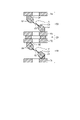
- FIG. 2 is a first schematic diagram for explaining the configuration of the main part of the pulse power supply device according to Embodiment 1.
- FIG. 1 The same components as in FIG. 1 are given the same reference numerals.
- the first electrode 31 is erected and fixed to the first electrode support plate 71 by a screw structure or the like.
- the second electrode 32 is erected on the second electrode support plate 72 by a screw structure or the like and fixed to the second electrode support plate 72 .
- the first electrode 31 and the second electrode 32 are arranged so as to face each other with their standing axes shifted.
- the third electrode 51 is erected on the third electrode support plate 73 by a screw structure or the like and fixed to the third electrode support plate 73 .
- the fourth electrode 52 is erected on the fourth electrode support plate 74 by a screw structure or the like and fixed to the fourth electrode support plate 74 .
- the third electrode 51 and the fourth electrode 52 are arranged so as to face each other with their standing axes shifted.
- each surface of the first electrode support plate 71, the second electrode support plate 72, the third electrode support plate 73, and the fourth electrode support plate 74, which are fixed by a screw structure or the like, is referred to as a "fixed portion".
- Each electrode of the first electrode 31, the second electrode 32, the third electrode 51 and the fourth electrode 52 is made of a conductive material such as metal.
- Each electrode may have a rotating body structure with a central axis.
- An example of a body of revolution structure is a cylinder.
- a structure that is a rotating body structure can be simply and easily manufactured using a machine tool such as a lathe.
- the surfaces facing the respective paired electrodes may be flat or rounded.
- the curvature of the rounding is desirably at least 1 mm or more.
- the electric field can be concentrated at each tip of the rounding, so that each gap switch can be operated at a lower voltage.
- the surfaces facing each other are flat surfaces, it is possible to obtain the effect of reducing electrode wear during repeated use.
- the first capacitor 20 it is desirable to use a capacitor that has excellent voltage resistance and a higher capacitance.
- a capacitor that has excellent voltage resistance and a higher capacitance.
- the first electrode support plate 71, the second electrode support plate 72, the third electrode support plate 73, and the fourth electrode support plate 74 are made of a conductive material such as metal.
- the surfaces of the electrode support plates, which are the fixing portions be configured such that the normals of the surfaces are parallel to each other. be.
- each electrode support plate be fixed with an insulating jig or the like.
- FIG. 3 is a second schematic diagram for explaining the configuration of the main part of the pulse power supply device according to Embodiment 1.
- FIG. 4 is a third schematic diagram for explaining the configuration of the main part of the pulse power supply device according to the first embodiment.
- the same components as in FIGS. 1 and 2 are denoted by the same reference numerals.
- the discharge for closing the switch is formed in the shortest path between the pair of electrodes.
- the line segment representing this shortest path is called a "short-circuit line".
- a line segment connecting the shortest path between the first electrode 31 and the second electrode 32 is defined as a first short-circuit line 60
- the shortest path between the third electrode 51 and the fourth electrode 52 is is a second short-circuit line 62 .
- a line segment connecting a first middle point 61, which is the middle point that bisects the first short-circuit line 60, and a second middle point 63, which is the middle point that bisects the second short-circuit line 62, is the first line segment.
- each electrode is configured such that the first angle ⁇ is greater than 0 degrees and less than 90 degrees.
- FIG. 4 shows, as an example of a direct exposure line, a direct exposure line 66 connecting an end point 68 of the second short circuit line 62 on the side of the fourth electrode 52 and an arbitrary point 65 on the first short circuit line 60.
- Holes 77, 78 and 79 are formed in the second electrode support plate 72, the third electrode support plate 73 and the first capacitor 20, respectively.
- at least one of the third electrode 51 and the fourth electrode 52 can be exposed to part of the discharge light generated by the discharge when the first gap switch 30 operates.
- light emission of the second gap switch 50 is promoted.
- the effect of shortening the delay time from the operation of the first gap switch 30 to the operation of the second gap switch 50 can be obtained.
- the current path from the first electrode support plate 71 to the fourth electrode support plate 74 can be shortened. The shorter the current path, the smaller the inductance parasitic on this current path. Therefore, the shorter the current path, the faster the rise of the high voltage pulse.
- the extent of the action of shortening the delay time and the action of speeding up the rise of the high voltage pulse is determined based on the sine wave function. For this reason, it is desirable to provide a margin of 18 degrees corresponding to a 5% value at which both effects are significant. For example, if the first angle ⁇ is less than 18 degrees, the effect of shortening the delay time cannot be significantly obtained. Conversely, if the first angle ⁇ is greater than 72 degrees, the effect of accelerating the rise of the high voltage pulse cannot be significantly obtained. For this reason, it is desirable to set at least one of the constraint conditions "18 degrees or more" or "72 degrees or less" as the first angle ⁇ .
- the larger angle is called a "second angle” and denoted by " ⁇ ".
- ⁇ the larger angle
- the second angle ⁇ is 180 degrees, it is a condition in which exposure cannot be performed geometrically, similarly to when the first angle ⁇ is 0 degrees. Therefore, if a margin of 18 degrees is provided as with the first angle ⁇ , the condition is 162 degrees or less.
- a specular body that reflects the discharge light may be arranged near the first electrode 31 and the fourth electrode 52 .
- the mirror assists in exposing at least one of the third electrode 51 and the fourth electrode 52 to part of the discharge light generated when the first gap switch 30 operates.
- the aforementioned holes 77, 78, 79 may be formed for direct exposure rays passing through the specular body. Therefore, the use of a specular body has the effect of increasing the degree of freedom in design.
- the specular body may be constructed using an optical element such as a mirror, or it may be constructed using a metallic surface with a mirror finish.
- the use of optical elements has the advantage of high reflectance. Using a metal surface has the advantage of being inexpensive.
- Holes 77 , 78 , and 79 provided in second electrode support plate 72 , third electrode support plate 73 , and first capacitor 20 are located between arbitrary point 65 on first short-circuit line 60 and second short-circuit line 62 .
- Any structure and any shape may be used as long as the exposure line 66 is formed directly between the end point 68 or the end point 69 .
- the structure forming the direct exposure line 66 may not be a hole, but may have a notch. Also, the holes or notches may not necessarily be formed.
- the portions through which the direct exposure rays 66 pass may be made of a transparent material such as acrylic.
- the first gap switch 30 and the second gap switch 50 can have different discharge atmospheres such as pressure.
- FIG. 5 is a schematic diagram for explaining the configuration of main parts in the modification of the pulse power supply device according to Embodiment 1.
- the first electrode 31 and the second electrode 32 have a rotating body structure having central axes 91 and 92, respectively, and the facing surfaces of the electrodes form curved surfaces.
- the central axes 91, 92 are parallel to each other.
- the angle formed by the central axis 91 and the first short-circuit line 60 is called a "third angle" and is represented by " ⁇ ”.
- the angle formed by the central axis 92 and the first short-circuit line 60 is also " ⁇ ".
- the third electrode 51 and the fourth electrode 52 have a rotating body structure with central axes 93 and 94, respectively, and the facing surfaces of the respective electrodes form curved surfaces.
- the central axes 93, 94 are parallel to each other.
- the angle formed by the central axis 93 and the second short-circuit line 62 is called a "fourth angle" and is represented by “.delta.”.
- the angle between the central axis 94 and the second short-circuit line 62 is also ".delta.”.
- the third angle ⁇ and the fourth angle ⁇ may be the same angle or may be different.
- At least one of the third angle ⁇ and the fourth angle ⁇ is 18 degrees or less, which corresponds to a 5% value of the sine wave function.
- Each electrode shown in FIG. 5 has a structure in which none of them are arranged perpendicularly to the fixing portion of the first electrode support plate 71, the second electrode support plate 72, the third electrode support plate 73, or the fourth electrode support plate 74. .
- the structure of each electrode becomes complicated, there is an advantage that consumption of the electrodes can be suppressed, so that an effect of mitigating the effects of deterioration over time can be obtained.
- the pulse power supply device includes the first capacitor, the first gap switch, and the second gap switch.
- the first gap switch has a first electrode and a second electrode.
- the second gap switch has a third electrode and a fourth electrode.
- a third electrode is connected to the second electrode through the first capacitor.
- the fourth electrode is positioned opposite the second electrode with respect to the third electrode.
- a first gap-switch axis which is a line segment connecting a first midpoint that is the midpoint of the first short-circuit line and a second midpoint that is the midpoint of the second short-circuit line, and the first short-circuit line.
- a first angle which is the smaller of the angles, is set to be greater than 0 degrees and less than 90 degrees.
- the pulse power supply device configured in this manner, the action of shortening the delay time from the operation of the first gap switch to the action of the second gap switch and the action of speeding up the rise of the high voltage pulse are achieved. You can strike a balance between As a result, it is possible to obtain the effect of being able to output a high voltage pulse with good energy efficiency.
- the first angle may be set to be 18 degrees or more and 72 degrees or less. With this setting, it is possible to shorten the delay time from the operation of the first gap switch to the operation of the second gap switch, and at the same time, to speed up the rise of the high voltage pulse.
- the second electrode support plate supporting the second electrode, the third electrode support plate supporting the third electrode, and the portion through which the direct exposure light passes in the first capacitor are made of a transparent material.
- a hole or notch may be formed in the portion through which the direct exposure rays pass.
- a direct exposure line is a line segment connecting at least one end point on the second shorting line and any point on the first shorting line.
- At least one set of the set of the first electrode and the second electrode and the set of the third electrode and the fourth electrode may have a rounded surface facing the paired electrode. good. Also, instead of this configuration, the surfaces facing the respective paired electrodes may form curved surfaces. With this configuration, it is possible to obtain the effect that the gap switch can be operated at a lower voltage.
- At least one pair of the pair of the first electrode and the second electrode and the pair of the third electrode and the fourth electrode may have plane surfaces facing each other.
- each electrode of at least one of the set of the first electrode and the second electrode and the set of the third electrode and the fourth electrode may have a rotating body structure having a central axis.
- each electrode has a rotating body structure having a central axis, it can be manufactured simply and easily using a machine tool such as a lathe.
- the angle between the central axis and the first short-circuit line or the angle between the central axis and the second short-circuit line should be 18 degrees or less. It should be set. With this configuration, it is possible to obtain the effect of shortening the delay time and the effect of speeding up the rise of the high voltage pulse.
- the pulse power supply device may include a mirror body that reflects discharge light generated when the first gap switch operates.
- a specular body When a specular body is used, the holes or notches provided in the second electrode supporting plate, the third electrode supporting plate and the first capacitor may be formed with respect to direct exposure rays passing through the specular body. Therefore, the use of a specular body has the effect of increasing the degree of freedom in design.
- Embodiment 2 is intended to further expand the functions of the pulse power supply device according to Embodiment 1 by changing the arrangement of some components.
- symbol is attached
- FIG. 6 is a first schematic diagram for explaining the configuration of the main part of the pulse power supply device according to Embodiment 2.
- FIG. FIG. 7 is a second schematic diagram for explaining the configuration of the main part of the pulse power supply device according to the second embodiment.
- the arrangement of the third electrode 51 and the fourth electrode 52 is different from that of the pulse power supply according to Embodiment 1 shown in FIG. is different.
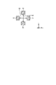
- FIGS. 7 shows an example of the positional relationship of the first electrode 31, the second electrode 32, the third electrode 51 and the fourth electrode 52 in the xy plane.
- the configuration of the second embodiment is a configuration in which only the positions of the third electrode 51 and the fourth electrode 52 are changed with respect to the first embodiment, and the shape and material are the same as those of the first embodiment.
- the first short-circuit line 60 and the second short-circuit line 62 are oriented in different directions.
- An electrode 52 is arranged. Therefore, the direct exposure line 66 for the second short-circuit line 62 can be three-dimensionally provided.
- the third electrode 51 or the fourth electrode 52 can receive the discharge light generated when the first gap switch 30 operates with a wider electrode area. As a result, the effect of shortening the delay time from the operation of the first gap switch 30 to the operation of the second gap switch 50 can be obtained more significantly.
- the third electrode 51 and the fourth electrode 52 are arranged such that the first short-circuit line 60 and the second short-circuit line 62 face different directions in the zx plane and the xy plane. but not limited to this example.
- the third electrode is arranged such that the first short-circuit line 60 and the second short-circuit line 62 face different directions in at least one plane of the xy plane, the yz plane, and the zx plane in the three-dimensional space.
- 51 and the fourth electrode 52 need only be arranged, and the above-described effect of enlarging the light receiving area can be obtained.
- the third electrode is arranged such that the first short-circuit line and the second short-circuit line face different directions in at least one plane in the three-dimensional space. and a fourth electrode. Therefore, the third electrode or the fourth electrode can receive the discharge light generated when the first gap switch operates with a wider electrode area. As a result, the effect of shortening the delay time from the operation of the first gap switch to the operation of the second gap switch can be obtained more significantly.
- the smaller angle between the direction of the first short-circuit line and the direction of the second short-circuit line is called a "fifth angle".
- This fifth angle is preferably 18 degrees or greater, corresponding to the 5% value of the sine wave function.
- Embodiment 3 aims to further expand the function by adding some components to the pulse power supply devices according to the first and second embodiments. It should be noted that, hereinafter, the same reference numerals are given to components that perform the same functions as those in the first and second embodiments, and overlapping descriptions will be omitted as appropriate.
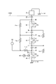
- FIG. 8 is a diagram showing the circuit configuration of the pulse power supply device according to the third embodiment.
- FIG. 8 shows a pulse power supply circuit 100A showing an example of the circuit configuration of the pulse power supply according to the third embodiment.
- a third gap switch 80, a third capacitor 22, a current limiting resistor 11c and a resistor 15a are added to the configuration of FIG. .
- the first gap switch 30, the first capacitor 20, the second gap switch 50, the second capacitor 21, the third gap switch 80 and the third capacitor 22 are connected in series in this order to form a series circuit. configure.
- the first gap switch 30 is positioned at one end of the series circuit
- the third capacitor 22 is positioned at the other end of the series circuit.
- the third gap switch 80 has a fifth electrode 81 and a sixth electrode 82 .
- the fifth electrode 81 is connected through the second capacitor 21 to the fourth electrode 52 of the second gap switch 50
- the sixth electrode 82 is connected to one end of the third capacitor 22 . That is, the sixth electrode 82 is arranged on the side opposite to the fourth electrode 52 of the second gap switch 50 with respect to the fifth electrode 81 .
- One end of the load 70 is connected to the other end of the third capacitor 22 .
- One end of the resistor 15a is connected to the connecting portion 14 where one end of the resistor 15, the other end of the first capacitor 20, and the third electrode 51 of the second gap switch 50 are connected.
- the other end of the resistor 15a is connected to a connecting portion 84 to which the other end of the second capacitor 21 and the fifth electrode 81 of the third gap switch 80 are connected. That is, the connecting portion 84 is connected to the connecting portion 14 via the resistor 15a.
- a reactor may be used instead of the resistor 15a.
- a connecting portion 85 to which the third gap switch 80 and the third capacitor 22 are connected is connected to the DC power supply 10 via current limiting resistors 11b and 11c.
- the fifth electrode 81 and the sixth electrode 82 are arranged apart from each other.
- a space separated by the fifth electrode 81 and the sixth electrode 82 constitutes a discharge gap 83 .
- a discharge path is formed by the discharge gap 83 when the third gap switch 80 discharges.
- the third gap switch 80 opens and closes an electrical switch.
- the circuit configuration of FIG. 8 is configured such that when the first gap switch 30 is closed, the second gap switch 50 and the third gap switch 80 are also closed together.
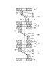
- FIG. 9 is a schematic diagram for explaining the configuration of the main part of the pulse power supply device according to Embodiment 3.
- FIG. 9 The same components as those in FIG. 8 are given the same reference numerals.
- the fifth electrode 81 is erected and fixed to the fifth electrode support plate 75 by a screw structure or the like.
- the sixth electrode 82 is erected on the sixth electrode support plate 76 by a screw structure or the like and fixed to the sixth electrode support plate 76 .
- the fifth electrode 81 and the sixth electrode 82 are arranged so as to face each other with their standing axes shifted.
- each surface of the fifth electrode support plate 75 and the sixth electrode support plate 76, which are fixed by a screw structure or the like, is sometimes referred to as a "fixed portion".
- the fifth electrode 81 and the sixth electrode 82 are made of a conductive material such as metal, like the other electrodes.
- the fifth electrode 81 and the sixth electrode 82 may have a rotating body structure having a central axis.
- An example of a body of revolution structure is a cylinder.
- a structure that is a rotating body structure can be simply and easily manufactured using a machine tool such as a lathe.
- the surfaces facing the respective paired electrodes may be flat or rounded.
- the curvature of the rounding is desirably at least 1 mm or more.
- the electric field can be concentrated at each tip of the rounding, so that each gap switch can be operated at a lower voltage.
- the surfaces facing each other are flat surfaces, it is possible to obtain the effect of reducing electrode wear during repeated use.
- the fifth electrode support plate 75 and the sixth electrode support plate 76 are made of a conductive material such as metal, like the other electrode support plates.
- a conductive material such as metal, like the other electrode support plates.
- the surfaces of the electrode support plates, which are the fixing portions be configured such that the normals of the surfaces are parallel to each other. be.
- each electrode support plate be fixed with an insulating jig or the like.
- a line segment connecting the shortest path between the fifth electrode 81 and the sixth electrode 82 is a third short-circuit line 86 .
- a line segment connecting a second middle point 63, which is the middle point dividing the second short-circuit line 62 into two equal parts, and a third middle point 87, which is the middle point dividing the third short-circuit line 86 into two equal parts, is the second line segment.
- An axis 88 between gap switches is used. Further, of the angles formed by the third short-circuit line 86 and the axis 88 between the second gap switches, the smaller angle is called a "sixth angle" and is represented by " ⁇ ". At this time, the sixth angle ⁇ is set to be smaller than the first angle ⁇ .
- the third gap switch 80 has a structure that prioritizes shortening the current path over exposure.
- a higher potential difference is generated in the third gap switch 80 than in the second gap switch 50 due to the characteristics of the circuit configuration of the pulse power supply circuit 100A. This is because the third gap switch 80 requires a small exposure area.
- the effect of shortening the delay time between the gap switches and the effect of speeding up the rise of the high voltage pulse can both be efficiently achieved.
- the pulse power supply device includes the fifth electrode connected to the fourth electrode of the second gap switch via the second capacitor, and the fourth electrode connected to the fifth electrode.
- a third gap switch having a sixth electrode disposed on the opposite side;
- a second inter-gap-switch axis which is a line segment connecting a second midpoint that is the midpoint of the second short-circuit line and a third midpoint that is the midpoint of the third short-circuit line, and the third short-circuit line.
- a smaller one of the angles is set to be smaller than the first angle.
Landscapes
- Generation Of Surge Voltage And Current (AREA)
Priority Applications (2)
| Application Number | Priority Date | Filing Date | Title |
|---|---|---|---|
| PCT/JP2021/016447 WO2022224439A1 (ja) | 2021-04-23 | 2021-04-23 | パルス電源装置 |
| JP2023516001A JP7511748B2 (ja) | 2021-04-23 | 2021-04-23 | パルス電源装置 |
Applications Claiming Priority (1)
| Application Number | Priority Date | Filing Date | Title |
|---|---|---|---|
| PCT/JP2021/016447 WO2022224439A1 (ja) | 2021-04-23 | 2021-04-23 | パルス電源装置 |
Publications (1)
| Publication Number | Publication Date |
|---|---|
| WO2022224439A1 true WO2022224439A1 (ja) | 2022-10-27 |
Family
ID=83723467
Family Applications (1)
| Application Number | Title | Priority Date | Filing Date |
|---|---|---|---|
| PCT/JP2021/016447 Ceased WO2022224439A1 (ja) | 2021-04-23 | 2021-04-23 | パルス電源装置 |
Country Status (2)
| Country | Link |
|---|---|
| JP (1) | JP7511748B2 (https=) |
| WO (1) | WO2022224439A1 (https=) |
Citations (3)
| Publication number | Priority date | Publication date | Assignee | Title |
|---|---|---|---|---|
| JPS56148183A (en) * | 1980-04-16 | 1981-11-17 | Nissin Electric Co Ltd | Impulse voltage generating device |
| JPH0435690U (https=) * | 1990-07-23 | 1992-03-25 | ||
| JP2002263471A (ja) * | 2001-03-06 | 2002-09-17 | Nippon Paint Co Ltd | マルクス回路を用いたプラズマ処理方法及びプラズマ処理装置 |
-
2021
- 2021-04-23 WO PCT/JP2021/016447 patent/WO2022224439A1/ja not_active Ceased
- 2021-04-23 JP JP2023516001A patent/JP7511748B2/ja active Active
Patent Citations (3)
| Publication number | Priority date | Publication date | Assignee | Title |
|---|---|---|---|---|
| JPS56148183A (en) * | 1980-04-16 | 1981-11-17 | Nissin Electric Co Ltd | Impulse voltage generating device |
| JPH0435690U (https=) * | 1990-07-23 | 1992-03-25 | ||
| JP2002263471A (ja) * | 2001-03-06 | 2002-09-17 | Nippon Paint Co Ltd | マルクス回路を用いたプラズマ処理方法及びプラズマ処理装置 |
Also Published As
| Publication number | Publication date |
|---|---|
| JP7511748B2 (ja) | 2024-07-05 |
| JPWO2022224439A1 (https=) | 2022-10-27 |
Similar Documents
| Publication | Publication Date | Title |
|---|---|---|
| US20070159760A1 (en) | Methods and Systems Related to Pulsed Power | |
| TW202030930A (zh) | 天線系統 | |
| WO2022224439A1 (ja) | パルス電源装置 | |
| US4497011A (en) | Switching apparatus for changing the absolute value and the permanent magnetization direction of ferromagnetic bodies, e.g. of permanent magnets | |
| CN106972841A (zh) | 一种简化脉冲形成电路及ltd模块 | |
| CN112821191A (zh) | 半导体激光器驱动电路、多线激光器及多线激光雷达 | |
| CN117850168B (zh) | 一种电子束直写装置 | |
| Staples et al. | The SNS four-phase LEBT chopper | |
| WO2022251269A2 (en) | Rf impedance matching network with series-connected diode switches | |
| CN212364415U (zh) | 一种交流电过零点检测电路及芯片 | |
| Lavrinovich et al. | High-power capacitor-switch assemblies rated at 100 ns | |
| JP4067890B2 (ja) | 棒状除電装置 | |
| JP5772424B2 (ja) | プラズマ光源 | |
| CN111490756A (zh) | 一种时序产生电路 | |
| JPH0290500A (ja) | Rfノックアウト装置 | |
| JP6800378B2 (ja) | 電磁波発生器 | |
| Efanov | Gigawatt all-solid-state nano-and picosecond pulse generators for radar applications | |
| RU195797U1 (ru) | Импульсный лазерный полупроводниковый излучатель | |
| Bacqueyrisses et al. | Comparative study of two types of spark gap switches for parallel triggering | |
| JPWO2022224439A5 (https=) | ||
| JP5754594B2 (ja) | プラズマ光源とプラズマ光発生方法 | |
| SU934205A1 (ru) | Устройство дл измерени размеров неэлектропроводных участков на электропроводном основании | |
| JP2012119555A (ja) | プラズマ光源とプラズマ光発生方法 | |
| CN111246648A (zh) | 一种共轴的多脉冲输出的驱动机构 | |
| JP2893489B2 (ja) | 高周波加速集束装置 |
Legal Events
| Date | Code | Title | Description |
|---|---|---|---|
| 121 | Ep: the epo has been informed by wipo that ep was designated in this application |
Ref document number: 21937930 Country of ref document: EP Kind code of ref document: A1 |
|
| ENP | Entry into the national phase |
Ref document number: 2023516001 Country of ref document: JP Kind code of ref document: A |
|
| NENP | Non-entry into the national phase |
Ref country code: DE |
|
| 122 | Ep: pct application non-entry in european phase |
Ref document number: 21937930 Country of ref document: EP Kind code of ref document: A1 |