WO2022220124A1 - 半導体基板並びにその製造方法および製造装置、GaN系結晶体、半導体デバイス、電子機器 - Google Patents
半導体基板並びにその製造方法および製造装置、GaN系結晶体、半導体デバイス、電子機器 Download PDFInfo
- Publication number
- WO2022220124A1 WO2022220124A1 PCT/JP2022/016009 JP2022016009W WO2022220124A1 WO 2022220124 A1 WO2022220124 A1 WO 2022220124A1 JP 2022016009 W JP2022016009 W JP 2022016009W WO 2022220124 A1 WO2022220124 A1 WO 2022220124A1
- Authority
- WO
- WIPO (PCT)
- Prior art keywords
- semiconductor
- semiconductor substrate
- layer
- substrate according
- opening
- Prior art date
- Legal status (The legal status is an assumption and is not a legal conclusion. Google has not performed a legal analysis and makes no representation as to the accuracy of the status listed.)
- Ceased
Links
Images








Classifications
-
- C—CHEMISTRY; METALLURGY
- C30—CRYSTAL GROWTH
- C30B—SINGLE-CRYSTAL GROWTH; UNIDIRECTIONAL SOLIDIFICATION OF EUTECTIC MATERIAL OR UNIDIRECTIONAL DEMIXING OF EUTECTOID MATERIAL; REFINING BY ZONE-MELTING OF MATERIAL; PRODUCTION OF A HOMOGENEOUS POLYCRYSTALLINE MATERIAL WITH DEFINED STRUCTURE; SINGLE CRYSTALS OR HOMOGENEOUS POLYCRYSTALLINE MATERIAL WITH DEFINED STRUCTURE; AFTER-TREATMENT OF SINGLE CRYSTALS OR A HOMOGENEOUS POLYCRYSTALLINE MATERIAL WITH DEFINED STRUCTURE; APPARATUS THEREFOR
- C30B25/00—Single-crystal growth by chemical reaction of reactive gases, e.g. chemical vapour-deposition growth
- C30B25/02—Epitaxial-layer growth
- C30B25/04—Pattern deposit, e.g. by using masks
-
- C—CHEMISTRY; METALLURGY
- C23—COATING METALLIC MATERIAL; COATING MATERIAL WITH METALLIC MATERIAL; CHEMICAL SURFACE TREATMENT; DIFFUSION TREATMENT OF METALLIC MATERIAL; COATING BY VACUUM EVAPORATION, BY SPUTTERING, BY ION IMPLANTATION OR BY CHEMICAL VAPOUR DEPOSITION, IN GENERAL; INHIBITING CORROSION OF METALLIC MATERIAL OR INCRUSTATION IN GENERAL
- C23C—COATING METALLIC MATERIAL; COATING MATERIAL WITH METALLIC MATERIAL; SURFACE TREATMENT OF METALLIC MATERIAL BY DIFFUSION INTO THE SURFACE, BY CHEMICAL CONVERSION OR SUBSTITUTION; COATING BY VACUUM EVAPORATION, BY SPUTTERING, BY ION IMPLANTATION OR BY CHEMICAL VAPOUR DEPOSITION, IN GENERAL
- C23C16/00—Chemical coating by decomposition of gaseous compounds, without leaving reaction products of surface material in the coating, i.e. chemical vapour deposition [CVD] processes
- C23C16/04—Coating on selected surface areas, e.g. using masks
-
- C—CHEMISTRY; METALLURGY
- C23—COATING METALLIC MATERIAL; COATING MATERIAL WITH METALLIC MATERIAL; CHEMICAL SURFACE TREATMENT; DIFFUSION TREATMENT OF METALLIC MATERIAL; COATING BY VACUUM EVAPORATION, BY SPUTTERING, BY ION IMPLANTATION OR BY CHEMICAL VAPOUR DEPOSITION, IN GENERAL; INHIBITING CORROSION OF METALLIC MATERIAL OR INCRUSTATION IN GENERAL
- C23C—COATING METALLIC MATERIAL; COATING MATERIAL WITH METALLIC MATERIAL; SURFACE TREATMENT OF METALLIC MATERIAL BY DIFFUSION INTO THE SURFACE, BY CHEMICAL CONVERSION OR SUBSTITUTION; COATING BY VACUUM EVAPORATION, BY SPUTTERING, BY ION IMPLANTATION OR BY CHEMICAL VAPOUR DEPOSITION, IN GENERAL
- C23C16/00—Chemical coating by decomposition of gaseous compounds, without leaving reaction products of surface material in the coating, i.e. chemical vapour deposition [CVD] processes
- C23C16/22—Chemical coating by decomposition of gaseous compounds, without leaving reaction products of surface material in the coating, i.e. chemical vapour deposition [CVD] processes characterised by the deposition of inorganic material, other than metallic material
- C23C16/30—Deposition of compounds, mixtures or solid solutions, e.g. borides, carbides, nitrides
- C23C16/34—Nitrides
-
- C—CHEMISTRY; METALLURGY
- C30—CRYSTAL GROWTH
- C30B—SINGLE-CRYSTAL GROWTH; UNIDIRECTIONAL SOLIDIFICATION OF EUTECTIC MATERIAL OR UNIDIRECTIONAL DEMIXING OF EUTECTOID MATERIAL; REFINING BY ZONE-MELTING OF MATERIAL; PRODUCTION OF A HOMOGENEOUS POLYCRYSTALLINE MATERIAL WITH DEFINED STRUCTURE; SINGLE CRYSTALS OR HOMOGENEOUS POLYCRYSTALLINE MATERIAL WITH DEFINED STRUCTURE; AFTER-TREATMENT OF SINGLE CRYSTALS OR A HOMOGENEOUS POLYCRYSTALLINE MATERIAL WITH DEFINED STRUCTURE; APPARATUS THEREFOR
- C30B25/00—Single-crystal growth by chemical reaction of reactive gases, e.g. chemical vapour-deposition growth
- C30B25/02—Epitaxial-layer growth
- C30B25/18—Epitaxial-layer growth characterised by the substrate
- C30B25/186—Epitaxial-layer growth characterised by the substrate being specially pre-treated by, e.g. chemical or physical means
-
- C—CHEMISTRY; METALLURGY
- C30—CRYSTAL GROWTH
- C30B—SINGLE-CRYSTAL GROWTH; UNIDIRECTIONAL SOLIDIFICATION OF EUTECTIC MATERIAL OR UNIDIRECTIONAL DEMIXING OF EUTECTOID MATERIAL; REFINING BY ZONE-MELTING OF MATERIAL; PRODUCTION OF A HOMOGENEOUS POLYCRYSTALLINE MATERIAL WITH DEFINED STRUCTURE; SINGLE CRYSTALS OR HOMOGENEOUS POLYCRYSTALLINE MATERIAL WITH DEFINED STRUCTURE; AFTER-TREATMENT OF SINGLE CRYSTALS OR A HOMOGENEOUS POLYCRYSTALLINE MATERIAL WITH DEFINED STRUCTURE; APPARATUS THEREFOR
- C30B29/00—Single crystals or homogeneous polycrystalline material with defined structure characterised by the material or by their shape
- C30B29/10—Inorganic compounds or compositions
- C30B29/38—Nitrides
-
- C—CHEMISTRY; METALLURGY
- C30—CRYSTAL GROWTH
- C30B—SINGLE-CRYSTAL GROWTH; UNIDIRECTIONAL SOLIDIFICATION OF EUTECTIC MATERIAL OR UNIDIRECTIONAL DEMIXING OF EUTECTOID MATERIAL; REFINING BY ZONE-MELTING OF MATERIAL; PRODUCTION OF A HOMOGENEOUS POLYCRYSTALLINE MATERIAL WITH DEFINED STRUCTURE; SINGLE CRYSTALS OR HOMOGENEOUS POLYCRYSTALLINE MATERIAL WITH DEFINED STRUCTURE; AFTER-TREATMENT OF SINGLE CRYSTALS OR A HOMOGENEOUS POLYCRYSTALLINE MATERIAL WITH DEFINED STRUCTURE; APPARATUS THEREFOR
- C30B29/00—Single crystals or homogeneous polycrystalline material with defined structure characterised by the material or by their shape
- C30B29/10—Inorganic compounds or compositions
- C30B29/40—AIIIBV compounds wherein A is B, Al, Ga, In or Tl and B is N, P, As, Sb or Bi
- C30B29/403—AIII-nitrides
- C30B29/406—Gallium nitride
-
- H—ELECTRICITY
- H10—SEMICONDUCTOR DEVICES; ELECTRIC SOLID-STATE DEVICES NOT OTHERWISE PROVIDED FOR
- H10H—INORGANIC LIGHT-EMITTING SEMICONDUCTOR DEVICES HAVING POTENTIAL BARRIERS
- H10H20/00—Individual inorganic light-emitting semiconductor devices having potential barriers, e.g. light-emitting diodes [LED]
- H10H20/01—Manufacture or treatment
- H10H20/011—Manufacture or treatment of bodies, e.g. forming semiconductor layers
- H10H20/013—Manufacture or treatment of bodies, e.g. forming semiconductor layers having light-emitting regions comprising only Group III-V materials
- H10H20/0133—Manufacture or treatment of bodies, e.g. forming semiconductor layers having light-emitting regions comprising only Group III-V materials with a substrate not being Group III-V materials
- H10H20/01335—Manufacture or treatment of bodies, e.g. forming semiconductor layers having light-emitting regions comprising only Group III-V materials with a substrate not being Group III-V materials the light-emitting regions comprising nitride materials
-
- H—ELECTRICITY
- H10—SEMICONDUCTOR DEVICES; ELECTRIC SOLID-STATE DEVICES NOT OTHERWISE PROVIDED FOR
- H10H—INORGANIC LIGHT-EMITTING SEMICONDUCTOR DEVICES HAVING POTENTIAL BARRIERS
- H10H20/00—Individual inorganic light-emitting semiconductor devices having potential barriers, e.g. light-emitting diodes [LED]
- H10H20/80—Constructional details
- H10H20/81—Bodies
- H10H20/819—Bodies characterised by their shape, e.g. curved or truncated substrates
-
- H—ELECTRICITY
- H10—SEMICONDUCTOR DEVICES; ELECTRIC SOLID-STATE DEVICES NOT OTHERWISE PROVIDED FOR
- H10P—GENERIC PROCESSES OR APPARATUS FOR THE MANUFACTURE OR TREATMENT OF DEVICES COVERED BY CLASS H10
- H10P14/00—Formation of materials, e.g. in the shape of layers or pillars
- H10P14/20—Formation of materials, e.g. in the shape of layers or pillars of semiconductor materials
- H10P14/24—Formation of materials, e.g. in the shape of layers or pillars of semiconductor materials using chemical vapour deposition [CVD]
-
- H—ELECTRICITY
- H10—SEMICONDUCTOR DEVICES; ELECTRIC SOLID-STATE DEVICES NOT OTHERWISE PROVIDED FOR
- H10P—GENERIC PROCESSES OR APPARATUS FOR THE MANUFACTURE OR TREATMENT OF DEVICES COVERED BY CLASS H10
- H10P14/00—Formation of materials, e.g. in the shape of layers or pillars
- H10P14/20—Formation of materials, e.g. in the shape of layers or pillars of semiconductor materials
- H10P14/27—Formation of materials, e.g. in the shape of layers or pillars of semiconductor materials using selective deposition, e.g. simultaneous growth of monocrystalline and non-monocrystalline semiconductor materials
- H10P14/271—Formation of materials, e.g. in the shape of layers or pillars of semiconductor materials using selective deposition, e.g. simultaneous growth of monocrystalline and non-monocrystalline semiconductor materials characterised by the preparation of substrate for selective deposition
-
- H—ELECTRICITY
- H10—SEMICONDUCTOR DEVICES; ELECTRIC SOLID-STATE DEVICES NOT OTHERWISE PROVIDED FOR
- H10P—GENERIC PROCESSES OR APPARATUS FOR THE MANUFACTURE OR TREATMENT OF DEVICES COVERED BY CLASS H10
- H10P14/00—Formation of materials, e.g. in the shape of layers or pillars
- H10P14/20—Formation of materials, e.g. in the shape of layers or pillars of semiconductor materials
- H10P14/27—Formation of materials, e.g. in the shape of layers or pillars of semiconductor materials using selective deposition, e.g. simultaneous growth of monocrystalline and non-monocrystalline semiconductor materials
- H10P14/276—Lateral overgrowth
-
- H—ELECTRICITY
- H10—SEMICONDUCTOR DEVICES; ELECTRIC SOLID-STATE DEVICES NOT OTHERWISE PROVIDED FOR
- H10P—GENERIC PROCESSES OR APPARATUS FOR THE MANUFACTURE OR TREATMENT OF DEVICES COVERED BY CLASS H10
- H10P14/00—Formation of materials, e.g. in the shape of layers or pillars
- H10P14/20—Formation of materials, e.g. in the shape of layers or pillars of semiconductor materials
- H10P14/29—Formation of materials, e.g. in the shape of layers or pillars of semiconductor materials characterised by the substrates
-
- H—ELECTRICITY
- H10—SEMICONDUCTOR DEVICES; ELECTRIC SOLID-STATE DEVICES NOT OTHERWISE PROVIDED FOR
- H10P—GENERIC PROCESSES OR APPARATUS FOR THE MANUFACTURE OR TREATMENT OF DEVICES COVERED BY CLASS H10
- H10P14/00—Formation of materials, e.g. in the shape of layers or pillars
- H10P14/20—Formation of materials, e.g. in the shape of layers or pillars of semiconductor materials
- H10P14/29—Formation of materials, e.g. in the shape of layers or pillars of semiconductor materials characterised by the substrates
- H10P14/2901—Materials
-
- H—ELECTRICITY
- H10—SEMICONDUCTOR DEVICES; ELECTRIC SOLID-STATE DEVICES NOT OTHERWISE PROVIDED FOR
- H10P—GENERIC PROCESSES OR APPARATUS FOR THE MANUFACTURE OR TREATMENT OF DEVICES COVERED BY CLASS H10
- H10P14/00—Formation of materials, e.g. in the shape of layers or pillars
- H10P14/20—Formation of materials, e.g. in the shape of layers or pillars of semiconductor materials
- H10P14/29—Formation of materials, e.g. in the shape of layers or pillars of semiconductor materials characterised by the substrates
- H10P14/2901—Materials
- H10P14/2907—Materials being Group IIIA-VA materials
- H10P14/2908—Nitrides
-
- H—ELECTRICITY
- H10—SEMICONDUCTOR DEVICES; ELECTRIC SOLID-STATE DEVICES NOT OTHERWISE PROVIDED FOR
- H10P—GENERIC PROCESSES OR APPARATUS FOR THE MANUFACTURE OR TREATMENT OF DEVICES COVERED BY CLASS H10
- H10P14/00—Formation of materials, e.g. in the shape of layers or pillars
- H10P14/20—Formation of materials, e.g. in the shape of layers or pillars of semiconductor materials
- H10P14/29—Formation of materials, e.g. in the shape of layers or pillars of semiconductor materials characterised by the substrates
- H10P14/2901—Materials
- H10P14/2921—Materials being crystalline insulating materials
-
- H—ELECTRICITY
- H10—SEMICONDUCTOR DEVICES; ELECTRIC SOLID-STATE DEVICES NOT OTHERWISE PROVIDED FOR
- H10P—GENERIC PROCESSES OR APPARATUS FOR THE MANUFACTURE OR TREATMENT OF DEVICES COVERED BY CLASS H10
- H10P14/00—Formation of materials, e.g. in the shape of layers or pillars
- H10P14/20—Formation of materials, e.g. in the shape of layers or pillars of semiconductor materials
- H10P14/29—Formation of materials, e.g. in the shape of layers or pillars of semiconductor materials characterised by the substrates
- H10P14/2924—Structures
- H10P14/2925—Surface structures
-
- H—ELECTRICITY
- H10—SEMICONDUCTOR DEVICES; ELECTRIC SOLID-STATE DEVICES NOT OTHERWISE PROVIDED FOR
- H10P—GENERIC PROCESSES OR APPARATUS FOR THE MANUFACTURE OR TREATMENT OF DEVICES COVERED BY CLASS H10
- H10P14/00—Formation of materials, e.g. in the shape of layers or pillars
- H10P14/20—Formation of materials, e.g. in the shape of layers or pillars of semiconductor materials
- H10P14/29—Formation of materials, e.g. in the shape of layers or pillars of semiconductor materials characterised by the substrates
- H10P14/2926—Crystal orientations
-
- H—ELECTRICITY
- H10—SEMICONDUCTOR DEVICES; ELECTRIC SOLID-STATE DEVICES NOT OTHERWISE PROVIDED FOR
- H10P—GENERIC PROCESSES OR APPARATUS FOR THE MANUFACTURE OR TREATMENT OF DEVICES COVERED BY CLASS H10
- H10P14/00—Formation of materials, e.g. in the shape of layers or pillars
- H10P14/20—Formation of materials, e.g. in the shape of layers or pillars of semiconductor materials
- H10P14/32—Formation of materials, e.g. in the shape of layers or pillars of semiconductor materials characterised by intermediate layers between substrates and deposited layers
- H10P14/3202—Materials thereof
- H10P14/3214—Materials thereof being Group IIIA-VA semiconductors
- H10P14/3216—Nitrides
-
- H—ELECTRICITY
- H10—SEMICONDUCTOR DEVICES; ELECTRIC SOLID-STATE DEVICES NOT OTHERWISE PROVIDED FOR
- H10P—GENERIC PROCESSES OR APPARATUS FOR THE MANUFACTURE OR TREATMENT OF DEVICES COVERED BY CLASS H10
- H10P14/00—Formation of materials, e.g. in the shape of layers or pillars
- H10P14/20—Formation of materials, e.g. in the shape of layers or pillars of semiconductor materials
- H10P14/32—Formation of materials, e.g. in the shape of layers or pillars of semiconductor materials characterised by intermediate layers between substrates and deposited layers
- H10P14/3242—Structure
- H10P14/3244—Layer structure
- H10P14/3251—Layer structure consisting of three or more layers
-
- H—ELECTRICITY
- H10—SEMICONDUCTOR DEVICES; ELECTRIC SOLID-STATE DEVICES NOT OTHERWISE PROVIDED FOR
- H10P—GENERIC PROCESSES OR APPARATUS FOR THE MANUFACTURE OR TREATMENT OF DEVICES COVERED BY CLASS H10
- H10P14/00—Formation of materials, e.g. in the shape of layers or pillars
- H10P14/20—Formation of materials, e.g. in the shape of layers or pillars of semiconductor materials
- H10P14/34—Deposited materials, e.g. layers
- H10P14/3402—Deposited materials, e.g. layers characterised by the chemical composition
- H10P14/3414—Deposited materials, e.g. layers characterised by the chemical composition being group IIIA-VIA materials
- H10P14/3416—Nitrides
Definitions
- the present invention relates to semiconductor substrates and the like.
- Patent Document 1 discloses a method of forming a plurality of semiconductor layers corresponding to openings of a plurality of masks using an ELO (Epitaxial Lateral Overgrowth) method.
- ELO Epiaxial Lateral Overgrowth
- a semiconductor substrate includes a main substrate, a mask pattern located above the main substrate and including a mask portion, and first semiconductor portions located above (upper layer) the mask pattern and adjacent to each other. and a second semiconductor portion, wherein the first semiconductor portion includes a first lower edge located on the mask portion and a first protruding portion protruding toward the second semiconductor portion from the first lower edge.
- FIG. 1A and 1B are a plan view and a cross-sectional view showing the configuration of a semiconductor substrate according to the present embodiment
- FIG. FIG. 4 is a cross-sectional view showing another configuration of the semiconductor substrate according to the embodiment
- It is a flow chart which shows an example of a manufacturing method of a semiconductor substrate concerning this embodiment.
- 1 is a block diagram showing an example of a semiconductor substrate manufacturing apparatus according to an embodiment
- FIG. It is a flow chart which shows an example of a manufacturing method of a semiconductor device concerning this embodiment.
- FIG. 4 is a cross-sectional view showing an example of separation and spacing of element units; It is a schematic diagram which shows the structure of the electronic device which concerns on this embodiment.
- FIG. 1A and 1B are a plan view and a cross-sectional view showing the configuration of a semiconductor substrate according to Example 1;
- FIG. 4 is a cross-sectional view showing an example of lateral growth of an ELO semiconductor layer;
- 4 is a cross-sectional view showing another configuration of the semiconductor substrate according to Example 1;
- FIG. FIG. 4 is a cross-sectional view showing another configuration of the semiconductor substrate according to the embodiment;
- FIG. 4 is a plan view showing a step of separating an element portion in Example 1;
- FIG. 10 is a cross-sectional view showing a step of isolating element portions in Example 1;
- 4 is a cross-sectional view showing another configuration of the semiconductor substrate of Example 1.
- FIG. 1A and 1B are a plan view and a cross-sectional view showing the configuration of a semiconductor substrate according to Example 1;
- FIG. 4 is a cross-sectional view showing an example of lateral growth of an ELO semiconductor layer;
- 4 is a cross-section
- FIG. 4 is a cross-sectional view showing another configuration of the semiconductor substrate 10 of Example 1.
- FIG. FIG. 10 is a cross-sectional view showing another example of the separation of the element units;
- FIG. 10 is a cross-sectional view showing the configuration of a semiconductor substrate of Example 2;
- FIG. 11 is a cross-sectional view showing another configuration of the semiconductor substrate according to Example 2;
- FIG. 10 is a cross-sectional view showing another configuration of the semiconductor substrate of Example 2;
- FIG. 10 is a cross-sectional view showing another configuration of the semiconductor substrate of Example 2;
- FIG. 11 is a schematic cross-sectional view showing the configuration of Example 4;
- FIG. 12 is a cross-sectional view showing an example of application of the fourth embodiment to an electronic device;
- FIG. 11 is a schematic cross-sectional view showing the configuration of Example 5;
- FIG. 12 is a cross-sectional view showing the configuration of Example 6;
- FIG. 12 is a cross-sectional view showing the configuration of Example 7
- [Semiconductor substrate] 1A and 1B are a plan view and a cross-sectional view showing the configuration of a semiconductor substrate according to this embodiment.
- a semiconductor substrate 10 semiconductor wafer according to the present embodiment includes, as shown in FIG. , and a first semiconductor portion 8F and a second semiconductor portion 8S located above the mask pattern 6 and adjacent to each other, the first semiconductor portion 8F being located on the mask portion 5 and having a first lower edge 8c. , and a first protruding portion H1 that protrudes toward the second semiconductor portion 8S from the first lower edge 8c in plan view.
- the mask pattern 6 includes a first opening K1 and a second opening K2 adjacent to each other in a first direction (hereinafter referred to as the X direction), and a mask portion 5 located between the first opening K1 and the second opening K2.
- a first direction hereinafter referred to as the X direction
- a mask portion 5 located between the first opening K1 and the second opening K2.
- the first projecting portion H1 may have a structure that overhangs the first lower edge 8c in the X direction.
- the end surface of the first projecting portion H1 in FIG. 1 includes two surfaces, it is not limited to this, and may include only one surface, or may include three or more surfaces.
- the surface included in the end surface of the first projecting portion H1 may be planar or curved.
- the first protrusion H1 may have a plane EC that includes the first lower edge 8c and is non-perpendicular to the X direction.
- the semiconductor substrate 10 may have a base layer 4 including the seed portion 3S above the main substrate 1, and the first semiconductor portion 8F may be in contact with the seed portion 3S at the first opening K1.
- the first and second openings K1 and K2 may have a tapered shape (a shape in which the width narrows toward the base layer 4 side).
- the underlying layer 4 may be formed so as to overlap at least the first and second openings K1 and K2.
- a semiconductor substrate means a substrate including a semiconductor portion, and the main substrate 1 may be a semiconductor or may be a non-semiconductor.
- the main substrate 1 and the underlying layer 4 are collectively referred to as the underlying substrate UK, and the main substrate 1, the underlying layer 4 and the mask pattern 6 are sometimes referred to as the template substrate (ELO substrate) 7 .
- the first semiconductor portion 8F contains, for example, a nitride semiconductor.
- a GaN-based semiconductor is a semiconductor containing gallium atoms (Ga) and nitrogen atoms (N), and typical examples include GaN, AlGaN, AlGaInN, and InGaN.
- the first semiconductor portion 8F may be of a doped type (for example, an n-type containing donors) or a non-doped type.
- the first semiconductor portion 8F containing a GaN-based semiconductor can be formed by an ELO (Epitaxial Lateral Overgrowth) method, but another method may be used as long as it can realize low defects.
- ELO Epi Lateral Overgrowth
- a heterogeneous substrate having a lattice constant different from that of a GaN-based semiconductor is used as the main substrate 1
- a GaN-based semiconductor is used as the seed portion 3S
- an inorganic compound film is used as the mask pattern 6
- a GaN-based semiconductor is used as the mask portion 5.
- the thickness direction (Z direction) of the first semiconductor portion 8F is the ⁇ 0001> direction (c-axis direction) of the GaN-based crystal
- the width direction (first direction, X direction) is the ⁇ 11-20> direction (a-axis direction) of the GaN-based crystal
- the longitudinal direction (Y-direction) of the first and second openings K1 and K2 is the ⁇ 1-100> direction of the GaN-based crystal.
- m-axis direction A layer formed by the ELO method may be referred to as an ELO semiconductor layer (including the first semiconductor portion 8F).
- the first semiconductor portion 8F formed by the ELO method includes a dislocation inheriting portion NS that overlaps the first opening K1 in a plan view and a mask portion 5 in a plan view. part EK (transposition non-inherited part).
- an active layer for example, a layer in which electrons and holes combine
- the active layer can be provided so as to overlap the low defect portion EK in plan view.
- a portion of the first semiconductor portion 8F that overlaps the mask portion 5 in plan view is a GaN-based crystal that includes a GaN-based semiconductor and has an upper surface 8J and a lower surface 8U parallel to the (0001) plane (c-plane). Can also be configured.
- the density of non-threading dislocations in the cross section parallel to the ⁇ 0001> direction is the same as or higher than the density of threading dislocations in the top surface 8J, and the lower edge 8c parallel to the ⁇ 1-100> direction.
- a cross section parallel to the ⁇ 0001> direction is, for example, the (1-100) plane (m-plane) or the (11-20) plane (a-plane).
- Threading dislocations are dislocations (defects) extending from the lower surface or inside of the first semiconductor portion 8F to the surface or surface layer along the thickness direction (Z direction) of the first semiconductor portion 8F. Threading dislocations can be observed by performing CL (Cathode Luminescence) measurement on the surface (parallel to the c-plane) of the first semiconductor portion 8F.
- Non-threading dislocations are dislocations that are CL-measured in a cross section along a plane parallel to the thickness direction, and are mainly basal plane (c-plane) dislocations.
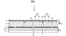
- FIG. 2 is a cross-sectional view showing another configuration of the semiconductor substrate according to this embodiment.
- the semiconductor substrate 10 includes a main substrate 1, an underlying layer 4, a mask pattern 6, first and second semiconductor portions 8F and 8S, and a first functional layer 9F above the first semiconductor portion 8F. and a second functional layer 9S above the second semiconductor portion 8S. overlaps.
- Each of the first and second functional layers 9F and 9S may be a single layer body or a laminate body.
- the first functional layer 9F may have at least one of a function as a component of a semiconductor device, an optical function, and a sensing function.
- the first semiconductor portion 8F has the first projecting portion H1. It becomes difficult for the raw material to reach the mask portion 5 located therebetween, and the formation of deposits is reduced. Further, since the first functional layer 9F formed above the first semiconductor portion 8F is difficult to be formed below the top portion 8P of the first protruding portion H1, the first functional layer 9F and the second functional layer 9S is less likely to be connected.
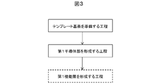
- FIG. 3 is a flow chart showing an example of a method for manufacturing a semiconductor substrate according to this embodiment.
- the step of preparing the template substrate (ELO growth substrate) 7 the step of forming the first semiconductor portion 8F using the ELO method is performed.
- the step of forming the first functional layer 9F can be performed as necessary.
- a mask pattern 6 may be formed on the underlying substrate UK.
- FIG. 4 is a block diagram showing an example of a semiconductor substrate manufacturing apparatus according to this embodiment.
- the semiconductor formation portion 72 has a first lower edge 8c positioned above the mask portion 5 and a first projecting portion H1 projecting in the X direction (a-axis direction) from the first lower edge 8c in plan view.
- 1 Semiconductor portion 8F (see FIG. 1) is formed by the ELO method.
- the semiconductor substrate manufacturing apparatus 70 may be configured to form the first functional layer 9F.
- the semiconductor formation section 72 may include an MOCVD apparatus, and the control section 74 may include a processor and memory.
- the control unit 74 may be configured to control the semiconductor forming unit 72 by executing a program stored in an internal memory, a communicable communication device, or an accessible network.
- This embodiment also includes a recording medium and the like.
- FIG. 5 is a flow chart showing an example of a method for manufacturing a semiconductor device according to this embodiment.
- FIG. 6 is a plan view showing an example of separation of the element portion.
- FIG. 7 is a cross-sectional view showing an example of separation and separation of element portions.
- the step of preparing the semiconductor substrate 10 after the step of preparing the semiconductor substrate 10, the step of forming the first functional layer 9F on the first semiconductor portion 8F is performed as necessary. Thereafter, as shown in FIGS. 6 and 7, a plurality of trenches TR (separation trenches) are formed in the semiconductor substrate 10 to cover the element portion DS (including the low defect portion EK of the first semiconductor portion 8F and the first functional layer 9F). ) is separated.
- trenches TR separation trenches
- Trench TR penetrates through first functional layer 9F and first semiconductor portion 8F.
- Base layer 4 and mask portion 5 may be exposed in trench TR.
- the opening width of trench TR can be equal to or greater than the width of first opening K1.
- the element portion DS is van der Waals coupled with the mask portion 5 and is a part of the semiconductor substrate 10 .
- the element portion DS is separated from the template substrate 7 to form a semiconductor device 20.
- the first functional layer 9F of the isolated element portion DS includes an end face 9x perpendicular to the X direction, but the end face 9x is not eroded by etching, so the first functional layer 9F (especially the active layer) is of good quality. is realized.
- the step of preparing the semiconductor substrate 10 shown in FIG. 5 may include each step of the semiconductor substrate manufacturing method shown in FIG.
- a semiconductor device 20 As shown in FIG. 7, by separating the element portion DS from the template substrate 7, a semiconductor device 20 (including, for example, a GaN-based crystal) can be formed. As a separation method, the semiconductor device 20 may be bonded to another carrier substrate using solder, or may be made using a flexible material such as an adhesive material or silicone elastomer polydimethylsiloxane (PDMS). It may be peeled off using an adhesive stamp.
- PDMS silicone elastomer polydimethylsiloxane
- semiconductor device 20 include light emitting diodes (LEDs), semiconductor lasers, Schottky diodes, photodiodes, transistors (including power transistors and high electron mobility transistors), and the like.
- LEDs light emitting diodes
- semiconductor lasers semiconductor lasers
- Schottky diodes Schottky diodes
- photodiodes transistors (including power transistors and high electron mobility transistors), and the like.
- FIG. 8 is a schematic diagram showing the configuration of the electronic device according to this embodiment.
- the electronic device 30 of FIG. 8 includes a semiconductor substrate 10 (a configuration that functions as a semiconductor device while including the template substrate 7, for example, when the template substrate 7 is translucent) and a driving substrate on which the semiconductor substrate 10 is mounted. 23 and a control circuit 25 that controls the drive board 23 .
- FIG. 9 is a schematic diagram showing another configuration of the electronic device according to this embodiment.
- An electronic device 30 of FIG. 9 includes a semiconductor device 20 including at least a low-defect portion EK, a drive board 23 on which the semiconductor device 20 is mounted, and a control circuit 25 that controls the drive board 23 .
- Examples of the electronic device 30 include a display device, a laser emitting device (including a Fabry-Perot type and a surface emitting type), a lighting device, a communication device, an information processing device, a sensing device, a power control device, and the like.
- Example 1 (overall structure) 10A and 10B are a plan view and a cross-sectional view showing the configuration of the semiconductor substrate according to the first embodiment.
- a semiconductor substrate 10 according to Example 1 includes a main substrate 1, a base layer 4 positioned above the main substrate 1, and first and second openings K1 and K2 adjacent in the X direction. , and a mask pattern 6 including a mask portion 5 located between the first and second openings K1 and K2, and first and second semiconductor portions 8F and 8S located above the mask pattern 6.
- the first and second semiconductor portions 8F and 8S are formed by the ELO method, are separated from each other, and are adjacent to each other. Note that the first and second semiconductor portions 8F and 8S may be referred to as ELO semiconductor layers 8 in some cases.
- the first and second semiconductor portions 8F and 8S can also be called first and second semiconductor layers.
- the first semiconductor part 8F has a first protruding part H1 that overlaps the first opening K1 in plan view and protrudes in the X direction (toward the second semiconductor part 8S) from the first lower edge 8c.
- the second semiconductor portion 8S overlaps the second opening portion K2 in a plan view, and a second overhang portion H2 overhangs in the opposite direction in the X direction (toward the first semiconductor portion 8F) from the second lower edge 8d.
- the lower edge means for example, the edge of the lower surface of the semiconductor layer portion
- the upper edge means, for example, the edge of the upper surface of the semiconductor layer portion.
- a heterosubstrate having a lattice constant different from that of the GaN-based semiconductor can be used for the main substrate 1 .
- hetero-substrates include single-crystal silicon (Si) substrates, sapphire (Al 2 O 3 ) substrates, silicon carbide (SiC) substrates, and the like.
- the plane orientation of the main substrate 1 is, for example, the (111) plane of a silicon substrate, the (0001) plane of a sapphire substrate, and the 6H—SiC (0001) plane of a SiC substrate. These are just examples, and any main substrate and plane orientation may be used as long as the ELO semiconductor layer 8 can be grown by the ELO method.
- a buffer layer 2 eg, AlN layer
- a seed layer 3 eg, nitride semiconductor
- the buffer layer 2 has a function of reducing, for example, the direct contact between the main substrate 1 and the seed layer 3 and the mutual melting.
- a silicon substrate or the like is used for the main substrate 1, it melts with the GaN-based semiconductor that is the seed layer 3. Therefore, by providing the buffer layer 2 such as an AlN layer, the melting is reduced.
- the main substrate 1 that does not melt together with the seed layer 3, which is a GaN-based semiconductor is used, a configuration without the buffer layer 2 is possible.
- An AlN layer which is an example of the buffer layer 2 can be formed to a thickness of about 10 nm to about 5 ⁇ m using, for example, an MOCVD apparatus.
- the buffer layer 2 may have at least one of the effect of increasing the crystallinity of the seed layer 3 and the effect of relieving the internal stress of the ELO semiconductor layer 8 .
- a GaN-based semiconductor containing Al for example, can be used for the seed layer 3 .
- the seed layer 3 includes a seed portion 3S (growing starting point of the ELO semiconductor layer) overlapping the first opening K1 of the mask pattern 6.
- a graded layer in which the Al composition approaches graded GaN may be used.
- the graded layer is, for example, a laminate in which an Al 0.7 Ga 0.3 N layer as a first layer and an Al 0.3 Ga 0.7 N layer as a second layer are provided in order from the buffer layer side is.
- the graded layer can be easily formed by MOCVD, and may be composed of three or more layers. By using a graded layer for the seed layer 3, the stress from the main substrate 1, which is a different substrate, can be relieved.
- the seed layer 3 can be configured to include a GaN layer. In this case, the seed layer 3 may be a single layer of GaN, or the uppermost layer of the graded layer that is the seed layer 3 may be a GaN layer.
- At least one of the buffer layer 2 (eg, aluminum nitride) and seed layer 3 (eg, GaN-based semiconductor) can also be deposited using a sputtering device (PSD: pulse sputter deposition, PLD: pulse laser deposition, etc.).
- PLD pulse sputter deposition
- PLD pulse laser deposition
- Mask pattern 6 (mask layer) includes mask portion 5 and first and second openings K1 and K2.
- the first and second openings K1 and K2 expose the seed portion 3S and have the function of growth start holes for starting the growth of the ELO semiconductor layer 8.
- the mask portion 5 allows the ELO semiconductor layer 8 to extend laterally. It may have a function of a selective growth mask for growing.
- the first and second openings K ⁇ b>1 and K ⁇ b>2 are portions (non-formation portions) of the mask pattern 6 where the mask portion 5 does not exist, and may not be surrounded by the mask portion 5 .
- SiOx silicon oxide film
- TiN titanium nitride film
- SiNx silicon nitride film
- SiON silicon oxynitride film
- a metal film having a high melting point for example, 1000° C. or higher.
- a single layer film containing any one of or a laminated film containing at least two of these can be used.
- a silicon oxide film having a thickness of about 100 nm to 4 ⁇ m (preferably about 150 nm to 2 ⁇ m) is formed on the underlying layer 4 by sputtering, and a resist is applied to the entire surface of the silicon oxide film.
- the resist is patterned by photolithography to form a resist having a plurality of striped openings.
- a portion of the silicon oxide film is removed by a wet etchant such as hydrofluoric acid (HF) or buffered hydrofluoric acid (BHF) to form a plurality of openings (including K1 and K2), and the resist is removed by organic cleaning.
- a mask pattern 6 is formed.
- the first and second openings K1 and K2 have a longitudinal shape (slit shape) and are periodically arranged in the a-axis direction (X direction) of the ELO semiconductor layer 8 .
- the widths of the first and second openings K1 and K2 are about 0.1 ⁇ m to 20 ⁇ m. As the width of each opening becomes smaller, the number of threading dislocations propagating from each opening into the ELO semiconductor layer 8 decreases. In addition, it becomes easy to separate (separate) the ELO semiconductor layer 8 from the template substrate 7 in a post-process. Furthermore, the area of the low-defect portion EK (for example, GaN-based crystal) with few surface defects can be increased.
- the silicon oxide film decomposes and evaporates in small amounts during the formation of the ELO semiconductor layer 8 and may be taken into the ELO semiconductor layer 8.
- the silicon nitride film and the silicon oxynitride film decompose and evaporate at high temperatures. It has the advantage of being difficult.
- the mask pattern 6 may be a single layer film of a silicon nitride film or a silicon oxynitride film, or may be a laminated film in which a silicon oxide film and a silicon nitride film are formed in this order on the base layer 4.
- 4 may be a laminated film in which a silicon nitride film and a silicon oxide film are formed in this order, or a laminated film in which a silicon nitride film, a silicon oxide film and a silicon nitride film are formed in this order on an underlying layer.
- a good mask pattern 6 can also be formed by using a general silicon oxide film (single layer) and using such a film formation method.
- a laminate was used in which a silicon oxide film (SiO 2 ) and a silicon nitride film (SiN) were formed in this order.
- the thickness of the silicon oxide film is, for example, 0.3 ⁇ m, and the thickness of the silicon nitride film is, for example, 70 nm.
- a plasma-enhanced chemical vapor deposition (CVD) method was used to form each of the silicon oxide film and the silicon nitride film.
- Example 1 (Formation of ELO semiconductor layer)
- the ELO semiconductor layer 8 was a GaN layer, and an ELO film of gallium nitride (GaN) was formed on the template substrate 7 by the MOCVD apparatus included in the semiconductor forming section 72 of FIG.
- substrate temperature 1120° C.
- growth pressure 50 kPa
- TMG trimethylgallium
- NH 3 15 slm
- V/III 6000 supply ratio
- the first and second semiconductor portions 8F and 8S are selectively grown on the seed portion 3S (the GaN layer which is the uppermost layer of the seed layer 3) exposed in the first and second openings K1 and K2. It grows laterally on the mask portion 5 . Then, the lateral growth of the first and second semiconductor portions 8F and 8S laterally grown from both sides on the mask portion 5 is stopped before they meet. Before the growth of the first and second semiconductor parts 8F and 8S is stopped, the lower inclined surface EC expands its area in an overhanging state without substantially changing the lower space Pc in FIG. A period may be included.
- the width Wm of the mask portion 5 is 50 ⁇ m
- the width of the first and second openings K1 and K2 is 5 ⁇ m
- the lateral width of the ELO semiconductor layer 8 is 53 ⁇ m
- the width (size in the X direction) of the low defect portion EK is 24 ⁇ m
- the ELO semiconductor The layer thickness of layer 8 was 5 ⁇ m.
- the ELO semiconductor layer 8 it is preferable to reduce mutual reaction between the ELO semiconductor layer 8 and the mask portion 5 so that the ELO semiconductor layer 8 and the mask portion 5 are brought into contact with each other by Van der Waals force.
- the lateral film formation rate is increased.
- a technique for increasing the lateral film formation rate is as follows. First, a vertical growth layer growing in the Z direction (c-axis direction) is formed on the seed portion 3S exposed from the first and second openings K1 and K2, and then grown in the X direction (a-axis direction). Form a lateral growth layer. At this time, by setting the thickness of the vertical growth layer to 10 ⁇ m or less, 5 ⁇ m or less, 3 ⁇ m or less, or 1 ⁇ m or less, the thickness of the horizontal growth layer can be kept low and the horizontal film formation rate can be increased.
- FIG. 11 is a cross-sectional view showing an example of lateral growth of an ELO semiconductor layer.
- an initial growth layer (part of the dislocation inheriting portion NS) SL is formed on the seed portion 3S, and then the first and second semiconductor portions 8F and 8S are grown laterally from the initial growth layer SL. It is desirable to grow The initial growth layer SL serves as a starting point for lateral growth of the first and second semiconductor portions 8F and 8S.
- the ELO film formation conditions it is possible to control the growth of the first and second semiconductor portions 8F and 8S in the Z direction (c-axis direction) or in the X direction (a-axis direction). be.
- the shape of the first and second overhangs H1 and H2 in FIG. 10 can also be controlled by the ELO film formation conditions (X-direction growth conditions).
- the edge of the initial growth layer SL is immediately before it rises on the upper surface of the mask portion 5 (at the stage when it is in contact with the upper end of the side surface of the mask portion 5), or 5 (that is, at this timing, the ELO film formation conditions are switched from the c-axis direction film formation conditions to the a-axis direction film formation conditions).
- the film formation in the lateral direction proceeds from the state where the initial growth layer SL slightly protrudes from the mask portion 5, so the material consumed for the growth in the thickness direction is reduced, and the first and second semiconductor portions 8F are formed.
- - 8S can be grown laterally at high speed.
- the initial growth layer SL can be formed with a thickness of 50 nm to 5.0 ⁇ m (eg, 80 nm to 2 ⁇ m).
- the thickness of the mask portion 5 and the thickness of the initial growth layer SL may be 500 nm or less.
- the initial growth layer SL is formed and then laterally grown to increase non-threading dislocations inside the low-defect portion EK (low-defect It is possible to reduce the threading dislocation density on the part EK surface. In addition, it is possible to control the distribution of impurity concentration (for example, silicon, oxygen) inside the low-defect portion EK.
- impurity concentration for example, silicon, oxygen
- the ratio of the width (WL) of the first semiconductor portion 8F to the width of the first opening K1 is 3.5 or more, 5.0 or more, 6.0 or more, 8.0. 10 or more, 15 or more, 20 or more, 30 or more, or 50 or more, and the ratio of low defect portions EK increases.
- the first and second semiconductor portions 8F and 8S shown in FIG. 11 can be nitride semiconductor crystals (for example, GaN crystals, AlGaN crystals, InGaN crystals, or InAlGaN crystals).
- the thickness of the vertical growth layer (initial growth layer) is set to 2 ⁇ m or more and the film formation is completed before the films growing laterally on the mask portion 5 meet each other, the thickness of the vertical growth layer It becomes difficult to supply the Ga raw material and the ammonia raw material to the gap portion, and the growth of the ELO semiconductor layer 8 under the end surface can be suppressed.
- the film is formed at a high temperature (for example, a film forming temperature of 1050° C. or higher) and a high V/III (>5000), a reverse tapered crystal face can be easily obtained.
- a temperature of 1150°C or less is preferable to a temperature exceeding 1200°C. It is possible to form the ELO semiconductor layer 8 even at a low temperature of less than 1000° C., which is preferable from the viewpoint of reducing mutual reaction.
- TMG trimethylgallium
- the raw material is not sufficiently decomposed, and gallium atoms and carbon atoms are simultaneously incorporated into the ELO semiconductor layer 8 in a larger amount than usual. rice field.
- film formation in the a-axis direction is fast and film formation in the c-axis direction is slow.
- the carbon incorporated into the ELO semiconductor layer 8 reduces the reaction with the mask portion 5 and reduces adhesion between the mask portion 5 and the ELO semiconductor layer 8. Therefore, when the ELO semiconductor layer 8 is deposited at a low temperature, the amount of ammonia supplied is reduced and the film is deposited at a low V/III ( ⁇ 1000), so that the carbon element in the raw material or the chamber atmosphere is taken into the ELO semiconductor layer 8. , the reaction with the mask portion 5 can be reduced.
- the ELO semiconductor layers (first and second semiconductor portions 8F and 8S) contain carbon.
- the first semiconductor portion 8F includes a first upper edge 8a located between the mask portion center 5c and the first opening K1 in plan view, and a mask portion center 5c in plan view.
- the second semiconductor portion 8S includes a second upper edge 8b positioned between the mask portion center 5c and the second opening K2 in plan view, and a portion between the mask portion center 5c and the second opening K2 in plan view.
- the second lower edge 8d located (located on the mask portion 5) and the second protruding portion H2 protruding in the X direction (first semiconductor portion 8F side) from the second lower edge 8d in plan view. have.
- the portion overlapping the mask portion 5 in plan view contains a GaN-based semiconductor and has an upper surface 8J and a lower surface 8U parallel to the (0001) plane (c-plane).
- GaN-based crystal GK has a non-threading dislocation density in a cross section parallel to the ⁇ 0001> direction higher than a threading dislocation density in the top surface 8J, and has a lower edge 8c parallel to the ⁇ 1-100> direction and a lower edge ⁇ 1-100> than the lower edge. 11-20> direction and an overhang portion (overhang portion) H1.
- the non-threading dislocation density of the GaN-based crystal GK can be 10 times or more, for example, 20 times or more the threading dislocation density.
- the threading dislocation density can be, for example, 5 ⁇ 10 6 [dislocations/cm 2 ] or less.
- the width (size in the X direction) of the GaN-based crystal body GK can be set to, for example, 10 ⁇ m or more. In the GaN-based crystal GK, while suppressing threading dislocations that affect the characteristics of semiconductor devices, non-threading dislocations, which have almost no effect, are present, which has the effect of relieving film stress.
- the non-penetrating dislocation density in the cross section parallel to the (11-20) plane (a-plane) was It may be larger than the dislocation density. Since the GaN-based crystal body GK is formed by growing in the lateral direction (X direction), impurities ( The concentration of atoms contained in the mask pattern 6, such as silicon and oxygen, can be low.
- Example 1 the maximum distance L1 between the first opening K1 and the first projecting portion H1 in the X direction is greater than the distance La between the first opening K1 and the first upper edge 8a. , the maximum distance L2 between the second opening K2 and the second protrusion H2 is greater than the distance Lb between the second opening K2 and the second upper edge 8b.
- the side surface ES of the first semiconductor part includes a lower inclined surface EC including the first lower edge 8c and an upper inclined surface EA including the first upper edge 8a, and is perpendicular to the lower inclined surface EC and the X direction.
- a first acute angle ⁇ 1 formed with the surface VF is smaller than a second acute angle ⁇ 2 formed between the upper inclined surface EA and the surface VF perpendicular to the X direction.
- the first acute angle ⁇ 1 may be 30° or less, 20° or less, or 15° or less.
- a distance Hp between the mask portion 5 and the top portion 8P of the first projecting portion is larger than half the thickness d1 of the first semiconductor portion 8F.
- the second acute angle ⁇ 2 may be 75° or more, 80° or more, or 85° or more.
- the minimum distance Px between the first semiconductor part 8F and the second semiconductor part 8S is the lower distance Pc indicating the distance between the first lower edge 8c and the second lower edge 8d, and the first upper edge 8a and the second upper edge 8b, which is smaller than the upper spacing Pa, and the upper spacing Pa is greater than the lower spacing Pc.
- the minimum spacing Px is, for example, 5 ⁇ m or less
- the lower spacing Pc is, for example, 7 ⁇ m or less
- the upper spacing Pa is, for example, 8 ⁇ m or less.
- the lower space Pc may be smaller than the opening widths of the first and second openings K1 and K2.
- the minimum spacing Px may be smaller than the opening widths of the first and second openings K1 and K2.
- the internal stress of the ELO semiconductor layer 8 is reduced, and cracks and defects occurring in the ELO semiconductor layer 8 are reduced. can be reduced. This effect is particularly great when the main substrate 1 is a different substrate.
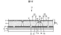
- FIG. 12 is a cross-sectional view showing another configuration of the semiconductor substrate according to Example 1.
- the first functional layer 9F is arranged on the first semiconductor section 8F
- the second functional layer 9S is arranged on the second semiconductor section 8S.
- the functional layers 9 are, for example, n-type semiconductor layers (eg, GaN-based), non-doped semiconductor layers (eg, GaN-based), p-type semiconductor layers (eg, GaN-based). system), a conductive layer, and an insulating layer.
- a non-doped semiconductor layer can also be used as an active layer (a layer in which electrons and holes combine).
- the functional layer 9 may be formed by any method.
- first projecting portion H1 is formed in the first semiconductor portion 8F and the second projecting portion H2 is formed in the second semiconductor portion 8S, when forming the first and second functional layers 9F and 9S, It becomes difficult for the raw materials (aluminum source, indium source) and the like to reach the mask portion 5 located between the first and second semiconductor portions 8F and 8S, and the formation of deposits is reduced. It is also possible to prevent the functional layers 9F and 9S from connecting to each other.
- the first functional layer 9F formed above the first semiconductor portion 8F is less likely to be formed below the top portion 8P of the first protruding portion H1, and is located above the second semiconductor portion 8S. Since the second functional layer 9S, which is formed on the upper layer, is less likely to be formed below the top portion 8Q of the second projecting portion H2, the first and second functional layers 9F and 9S are naturally separated during formation ( self-isolation). This improves the yield of the step of isolating the element portion DS.
- the active layer included in the first functional layer 9F has a shape that does not reach the first lower edge 8c
- the active layer included in the second functional layer 9S has a shape that does not reach the second lower edge 8d.
- a GaN-based p-type semiconductor layer for example, is formed in the functional layer 9, silicon and oxygen separated from the silicon-based mask pattern 6 (eg, silicon oxide film) are taken in to form a p-type dopant (eg, Mg). You may be compensated. If the ELO semiconductor layer 8 is a GaN-based n-type semiconductor, silicon or the like may separate from the ELO semiconductor layer 8 as well. In Example 1, the rise of the n-type dopant such as silicon is inhibited by the first and second protrusions H1 and H2. function can be enhanced.
- the first functional layer 9F includes a layer containing indium as a composition (for example, an In x Ga (1-x) N layer, where x is a positive number equal to or less than 1)
- In atoms are larger than Ga atoms.
- crystal defects and in-film stress may occur. , the stress in the film can be relaxed.
- the first functional layer 9F includes a layer containing aluminum as a composition (for example, an Al x Ga (1-x) N layer, where x is a positive number equal to or less than 1)
- a layer containing aluminum as a composition for example, an Al x Ga (1-x) N layer, where x is a positive number equal to or less than 1
- the Al composition increases, the ELO Due to lattice mismatch with the semiconductor layer 8, difference in thermal expansion coefficient, etc., crystal defects such as cracks, crystal slips on crystal planes (for example, m-plane slips in GnN-based semiconductor layers), and intra-film stress
- the first functional layer 9F by separating the first functional layer 9F from the other functional layers, propagation of crystal defects can be suppressed and intra-film stress can be alleviated.
- FIG. 13 is a cross-sectional view showing another configuration of the semiconductor substrate according to this embodiment.
- an edge growth 9G (corner) may occur as shown in FIG.
- the functional layer 9 includes an AlGaN layer.
- Edge growth can have a width of 10 ⁇ m or more and a size of about 200 to 300 nm in height, which hinders post-processes. 9G can be significantly reduced (for example, the height is 100 nm or less).
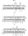
- FIG. 14A and 14B are plan views showing the process of separating the element portion in the first embodiment.
- 15A and 15B are cross-sectional views showing a step of isolating the element portions in the first embodiment.
- dry etching is used to form a plurality of trenches TR extending in the X direction to separate the element portions DS.
- the element portion DS is surrounded by two trenches TR and two gaps Gp extending in the Y direction, and the element portion DS larger than that in FIG. 6 can be separated. Dry etching is realized by a general photolithography method.
- the semiconductor substrate 10 is immersed in an etchant ET to dissolve the mask pattern 6, and then the surface of the ELO semiconductor layer 8 is covered with an adhesive tape (for example, a semiconductor wafer is diced).
- a Peltier element (not shown) may be used to lower the temperature of the semiconductor substrate 10 with the adhesive tape attached thereto.
- the adhesive tape which generally has a larger coefficient of thermal expansion than the semiconductor, shrinks greatly, and stress is applied to the ELO semiconductor layer 8 . Since the ELO semiconductor layer 8 is bonded only to the underlying layer 4 (seed portion) of the template substrate 7 and the mask portion 5 is removed, the stress from the adhesive tape is applied to the underlying layer (of the template substrate 7). 4 and can mechanically cleave or break the bond. That is, it is not necessary to etch away the joint.
- FIG. 16 is a cross-sectional view showing another configuration of the semiconductor substrate of Example 1.
- the semiconductor substrate 10 of FIG. 10 has dislocation inheriting portions NS (portions overlapping the first and second openings K1 and K2 in plan view) of the first and second semiconductor portions 8F and 8S. can also be removed. Further, it is also possible to remove portions of the base layer 4 that overlap the first and second openings K1 and K2 in plan view.
- FIG. 17 is a cross-sectional view showing another configuration of the semiconductor substrate 10 of Example 1.
- first and second functional layers 9F and 9S can also be provided on the first and second semiconductor portions 8F and 8S in FIG.
- FIG. 18 is a cross-sectional view showing another step of separating the element portions in Example 1.
- FIG. Since the ELO semiconductor layer 8 and the mask portion 5 in FIG. 17 are coupled by van der Waals force (weak force), as shown in FIG. etc.), the element portion DS can be easily peeled off from the template substrate, and the semiconductor device 20 can be obtained. Being able to peel off directly from the mask portion 5 using a viscoelastic elastomer stamp, an electrostatic adhesive stamp, or the like is a great advantage in terms of cost, throughput, and the like. After contacting the ELO semiconductor layer 8 with a viscoelastic elastomer stamp, an electrostatic adhesive stamp, or the like, for example, ultrasonic vibrations or the like may be applied. By this vibration or the like, the ELO semiconductor layer 8 can be peeled off from the mask portion 5 more easily.
- FIG. 19 is a cross-sectional view showing the configuration of the semiconductor substrate of Example 2.
- the first semiconductor portion 8F includes a first upper edge 8a positioned between the mask portion center 5c and the first opening K1 in plan view, and a first upper edge 8a positioned between the mask portion center 5c and the first opening K1 in plan view.
- a first lower edge 8c located on the mask portion 5) located between the first opening K1 and projecting in the X direction (toward the second semiconductor portion 8S) from the first lower edge 8c in plan view. and a first projecting portion H1.
- the second semiconductor portion 8S includes a second upper edge 8b positioned between the mask portion center 5c and the second opening K2 in plan view, and a portion between the mask portion center 5c and the second opening K2 in plan view.
- the second lower edge 8d located (located on the mask portion 5) and the second protruding portion H2 protruding in the X direction (first semiconductor portion 8F side) from the second lower edge 8d in plan view. have.
- the portion overlapping the mask portion 5 in plan view contains a GaN-based semiconductor and has an upper surface 8J and a lower surface 8U parallel to the (0001) plane (c-plane).
- GaN-based crystal GK has a non-threading dislocation density in a cross section parallel to the ⁇ 0001> direction higher than a threading dislocation density in the top surface 8J, and has a lower edge 8c parallel to the ⁇ 1-100> direction and a lower edge ⁇ 1-100> than the lower edge. 11-20> direction and an overhang portion (overhang portion) H1.
- the first upper edge 8a is the top of the first projecting portion H1
- the second upper edge 8b is the top of the second projecting portion H2.
- the distance La between the first opening K1 and the first upper edge 8a is greater than the distance Lc between the first opening K1 and the first lower edge 8c
- the second opening K2 and the second upper edge 8a are separated from each other.
- a distance Lb to the edge 8b is greater than a distance Ld between the second opening K2 and the second lower edge 8d.
- a gap Gp sandwiched between the first semiconductor portion 8F and the second semiconductor portion 8S has an inverse tapered shape that is wider on the mask portion 5 side.
- the upper spacing Pa indicating the spacing between the first upper edge 8a and the second upper edge 8b is smaller than 5 ⁇ m.
- the ratio of the upper spacing Pa to the width Wm of the mask portion is less than 0.5
- the ratio of the lower spacing Pc indicating the spacing between the first lower edge 8c and the second lower edge 8d to the width Wm of the mask portion is 0. less than .7.
- An acute angle ⁇ formed between a plane EF including the first upper edge 8a and the first lower edge 8c and a plane VF perpendicular to the X direction is 15° or less.
- FIG. 20 is a cross-sectional view showing another configuration of the semiconductor substrate according to the second embodiment.
- the first functional layer 9F is arranged on the first semiconductor section 8F
- the second functional layer 9S is arranged on the second semiconductor section 8S.
- the first functional layer 9F formed above the first semiconductor portion 8F is less likely to be formed below the top portion 8P of the first protruding portion H1 and is formed above the second semiconductor portion 8S. Since it is difficult to form the second functional layer 9S below the top portion 8Q of the second projecting portion H2, the first and second functional layers 9F and 9S are separated from each other. This improves the yield of the step of isolating the element portion DS.
- the rise of an n-type dopant such as silicon is greatly reduced by the first and second protrusions H1 and H2. It becomes difficult for the n-type dopant to be incorporated into the p-type semiconductor layer, and the function of the p-type semiconductor layer can be enhanced.
- FIG. 21 is a cross-sectional view showing another configuration of the semiconductor substrate of Example 2.
- the first semiconductor portion 8F includes a first upper edge 8a positioned between the mask portion center 5c and the first opening K1 in plan view, and a first upper edge 8a positioned between the mask portion center 5c and the first opening K1 in plan view, and a mask portion center 5c and the first opening K1 in plan view.
- a first lower edge 8c located on the mask portion 5) located between the first opening K1 and projecting in the X direction (toward the second semiconductor portion 8S) from the first lower edge 8c in plan view. and a first projecting portion H1.
- the second semiconductor portion 8S includes a second upper edge 8b positioned between the mask portion center 5c and the second opening K2 in plan view, and a portion between the mask portion center 5c and the second opening K2 in plan view.
- the second lower edge 8d located (located on the mask portion 5) and the second protruding portion H2 protruding in the X direction (first semiconductor portion 8F side) from the second lower edge 8d in plan view. have.
- the portion overlapping the mask portion 5 in plan view contains a GaN-based semiconductor and has an upper surface 8J and a lower surface 8U parallel to the (0001) plane (c-plane).
- GaN-based crystal GK has a non-threading dislocation density in a cross section parallel to the ⁇ 0001> direction higher than a threading dislocation density in the top surface 8J, and has a lower edge 8c parallel to the ⁇ 1-100> direction and a lower edge ⁇ 1-100> than the lower edge. 11-20> direction and an overhang portion (overhang portion) H1.
- the side surface ES (end surface) of the first semiconductor portion includes an upper inclined surface EA including the first upper edge 8a, a vertical surface EJ perpendicular to the X direction, and a first lower edge 8c. and a lower inclined plane EC.
- FIG. 22 is a cross-sectional view showing another configuration of the semiconductor substrate of Example 2.
- first and second functional layers 9F and 9S can also be provided on the first and second semiconductor portions 8F and 8S in FIG.
- the ELO semiconductor layer 8 is a GaN layer, but it is not limited to this.
- an InGaN layer which is a GaN-based semiconductor layer, can be formed. Lateral deposition of the InGaN layer is performed at low temperatures, eg, below 1000.degree. This is because, at high temperatures, the vapor pressure of indium increases and it is not effectively incorporated into the film. Lowering the film formation temperature has the effect of reducing the mutual reaction between the mask portion 5 and the InGaN layer. In addition, the InGaN layer has the effect of being less reactive with the mask portion 5 than the GaN layer.
- TAG triethylgallium
- FIG. 23 is a schematic cross-sectional view showing the configuration of Example 4.
- a functional layer 9 forming an LED is formed on the ELO semiconductor layer 8 .
- the ELO semiconductor layer 8 is of n-type doped with silicon or the like, for example.
- the functional layer 9 includes an active layer 34, an electron blocking layer 35, and a GaN-based p-type semiconductor layer 36 in order from the lower layer side.
- the active layer 34 is an MQW (Multi-Quantum Well) and includes an InGaN layer and a GaN layer.
- the electron blocking layer 35 is, for example, an AlGaN layer.
- the GaN-based p-type semiconductor layer 36 is, for example, a GaN layer.
- the anode 38 is arranged in contact with the GaN-based p-type semiconductor layer 36 and the cathode 39 is arranged in contact with the semiconductor layer 8 .
- a semiconductor device 20 including a GaN-based crystal
- films up to the ELO semiconductor layer 8 remove the semiconductor substrate 10 from the film forming apparatus, and then form the functional layer 9 using another apparatus.
- an n-type GaN layer may be inserted between the ELO semiconductor layer 8 and the functional layer 9 as an intermediate layer that serves as a buffer during regrowth.
- the thickness of the intermediate layer can be about 0.1 ⁇ m to about 3 ⁇ m.
- FIG. 24 is a cross-sectional view showing an example of application of the fourth embodiment to electronic equipment.
- a red micro-LED 20R, a green micro-LED 20G, and a blue micro-LED 20B can be obtained, and by mounting these on a drive substrate (TFT substrate) 23, a micro LED display 30D (electronic device) can be configured. can be done.
- a red micro-LED 20R, a green micro-LED 20G, and a blue micro-LED 20B are mounted on a plurality of pixel circuits 27 of the driving substrate 23 via a conductive resin 24 (for example, an anisotropic conductive resin) or the like, and then mounted on the driving substrate 23.
- a control circuit 25, a driver circuit 29, and the like are mounted.
- a portion of the driver circuit 29 may be included in the drive substrate 23 .
- Example 5 is a schematic cross-sectional view showing the configuration of Example 5.
- a functional layer 9 forming a semiconductor laser is formed on the ELO semiconductor layer 8 .
- the functional layer 9 includes, from the lower layer side, an n-type clad layer 41, an n-type guide layer 42, an active layer 43, an electron blocking layer 44, a p-type guide layer 45, a p-type clad layer 46, and a GaN-based p-type semiconductor layer. 47 included.
- An InGaN layer can be used for each of the guide layers 42 and 45 .
- a GaN layer or an AlGaN layer can be used for each of the clad layers 41 and 46 .
- the anode 48 is placed in contact with the GaN-based p-type semiconductor layer 47 and the cathode 49 is placed in contact with the ELO semiconductor layer 8 .
- a semiconductor device 20 including a GaN-based crystal
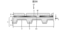
- FIG. 26 is a cross-sectional view showing the configuration of the sixth embodiment.
- a sapphire substrate having an uneven surface is used as the main substrate 1 .
- Underlayer 4 has buffer layer 2 and seed layer 3 .
- a GaN layer having a (20-21) plane is formed as the underlying layer 4 on the main substrate 1 .
- the ELO semiconductor layer 8 has the (20-21) plane, which is the main crystal plane, in the underlying layer 4, and the ELO semiconductor layer 8 having a semipolar plane can be obtained.
- a GaN layer having a (11-22) plane can also be formed as the base layer 4 on the main substrate 1 by using a sapphire substrate having an uneven surface.
- the underlying layer 4 may not be formed over the entire substrate. If the underlying layer 4 contains a material different from that of the main substrate 1, stress may be generated in the semiconductor substrate (ELO semiconductor layer, functional layer) due to differences in thermal expansion coefficient, lattice constant, and the like. Therefore, the underlying layer 4 (at least one of the buffer layer and the seed layer) may be locally provided so as to overlap each opening of the mask pattern 6 . A configuration in which the underlying layer 4 is not provided is also possible.
- FIG. 27 is a cross-sectional view showing the configuration of Embodiment 7.
- the template substrate (ELO growth substrate) 7 may be configured as shown in FIG. 27, for example.
- the template substrate 7 may be composed of the main substrate 1 and the mask pattern 6 (no underlying layer is provided), and the portion of the surface layer of the main substrate 1 overlapping the first opening K1 may function as a seed portion.
- the main substrate 1 a GaN bulk substrate, a 6H--SiC bulk substrate, or a 4H--SiC bulk substrate can be used as the main substrate 1.
- a bulk substrate is a wafer (free-standing substrate) cut from a bulk crystal.
- the template substrate 7 can be composed of the main substrate 1, the seed layer 3 (seed portion) locally arranged so as to overlap the first opening K1 in plan view, and the mask pattern 6.
- the main substrate 1 may be a silicon substrate and the seed layer 3 may contain AlN, or the main substrate 1 may be a silicon carbide substrate and the seed layer 3 may contain a GaN-based semiconductor.
- the template substrate 7 includes the main substrate 1, the buffer layer 2 covering the main substrate 1, the seed layer 3 (seed portion) locally arranged so as to overlap the first opening K1 in plan view, and the mask.
- Pattern 6 can be used.
- the main substrate 1 may be a silicon substrate
- the buffer layer 2 may contain at least one of AlN and SiC
- the seed layer 3 may contain a GaN-based semiconductor.
- the template substrate 7 is composed of the main substrate 1, the buffer layer 2 (buffer portion) locally arranged so as to overlap the first opening K1 in plan view, and the template substrate 7 so as to overlap the first opening K1 in plan view. It can be composed of a seed layer 3 (seed portion) and a mask pattern 6 which are locally arranged in the region.
- the main substrate 1 may be a silicon substrate
- the buffer layer 2 may contain at least one of AlN and silicon carbide
- the seed layer 3 may contain a GaN-based semiconductor.
Landscapes
- Chemical & Material Sciences (AREA)
- Engineering & Computer Science (AREA)
- Materials Engineering (AREA)
- Metallurgy (AREA)
- Organic Chemistry (AREA)
- Crystallography & Structural Chemistry (AREA)
- Inorganic Chemistry (AREA)
- Chemical Kinetics & Catalysis (AREA)
- General Chemical & Material Sciences (AREA)
- Mechanical Engineering (AREA)
- Recrystallisation Techniques (AREA)
Priority Applications (3)
| Application Number | Priority Date | Filing Date | Title |
|---|---|---|---|
| JP2023514588A JP7779906B2 (ja) | 2021-04-16 | 2022-03-30 | 半導体基板並びにその製造方法および製造装置、GaN系結晶体、半導体デバイス、電子機器 |
| US18/555,197 US20240191391A1 (en) | 2021-04-16 | 2022-03-30 | SEMICONDUCTOR SUBSTRATE, MANUFACTURING METHOD AND MANUFACTURING APPARATUS THEREFOR, GaN-BASED CRYSTAL BODY, SEMICONDUCTOR DEVICE, AND ELECTRONIC DEVICE |
| CN202280026769.3A CN117321257A (zh) | 2021-04-16 | 2022-03-30 | 半导体基板和其制造方法以及制造装置、GaN系晶体、半导体器件、电子设备 |
Applications Claiming Priority (2)
| Application Number | Priority Date | Filing Date | Title |
|---|---|---|---|
| JP2021069969 | 2021-04-16 | ||
| JP2021-069969 | 2021-04-16 |
Publications (1)
| Publication Number | Publication Date |
|---|---|
| WO2022220124A1 true WO2022220124A1 (ja) | 2022-10-20 |
Family
ID=83639631
Family Applications (1)
| Application Number | Title | Priority Date | Filing Date |
|---|---|---|---|
| PCT/JP2022/016009 Ceased WO2022220124A1 (ja) | 2021-04-16 | 2022-03-30 | 半導体基板並びにその製造方法および製造装置、GaN系結晶体、半導体デバイス、電子機器 |
Country Status (5)
| Country | Link |
|---|---|
| US (1) | US20240191391A1 (https=) |
| JP (1) | JP7779906B2 (https=) |
| CN (1) | CN117321257A (https=) |
| TW (1) | TWI841952B (https=) |
| WO (1) | WO2022220124A1 (https=) |
Cited By (2)
| Publication number | Priority date | Publication date | Assignee | Title |
|---|---|---|---|---|
| WO2024201629A1 (ja) * | 2023-03-27 | 2024-10-03 | 京セラ株式会社 | 半導体成長用テンプレート基板、半導体基板、半導体成長用テンプレート基板の製造方法および製造装置、並びに半導体基板の製造方法および製造装置 |
| WO2025115999A1 (ja) * | 2023-12-01 | 2025-06-05 | 京セラ株式会社 | 半導体基板およびその製造方法、半導体基板の製造装置、並びに半導体デバイス |
Citations (2)
| Publication number | Priority date | Publication date | Assignee | Title |
|---|---|---|---|---|
| JP2013532621A (ja) * | 2010-06-24 | 2013-08-19 | グロ アーベー | 配向されたナノワイヤー成長用のバッファ層を有する基板 |
| WO2019191760A1 (en) * | 2018-03-30 | 2019-10-03 | The Regents Of The University Of California | Method of fabricating non-polar and semi-polar devices using epitaxial lateral overgrowth |
Family Cites Families (5)
| Publication number | Priority date | Publication date | Assignee | Title |
|---|---|---|---|---|
| TWI638071B (zh) * | 2013-08-08 | 2018-10-11 | 三菱化學股份有限公司 | 自立GaN基板、GaN結晶、GaN單結晶之製造方法及半導體裝置之製造方法 |
| US10438792B2 (en) * | 2016-10-20 | 2019-10-08 | QROMIS, Inc. | Methods for integration of elemental and compound semiconductors on a ceramic substrate |
| CN112204754B (zh) | 2018-05-30 | 2024-08-13 | 加利福尼亚大学董事会 | 从半导体衬底移除半导体层的方法 |
| JP6626929B1 (ja) * | 2018-06-29 | 2019-12-25 | 京セラ株式会社 | 半導体デバイス及び電気装置 |
| CN114207847B (zh) * | 2019-08-13 | 2022-09-02 | 苏州晶湛半导体有限公司 | 氮化物半导体衬底的制作方法 |
-
2022
- 2022-03-30 US US18/555,197 patent/US20240191391A1/en active Pending
- 2022-03-30 WO PCT/JP2022/016009 patent/WO2022220124A1/ja not_active Ceased
- 2022-03-30 JP JP2023514588A patent/JP7779906B2/ja active Active
- 2022-03-30 CN CN202280026769.3A patent/CN117321257A/zh active Pending
- 2022-04-15 TW TW111114376A patent/TWI841952B/zh active
Patent Citations (2)
| Publication number | Priority date | Publication date | Assignee | Title |
|---|---|---|---|---|
| JP2013532621A (ja) * | 2010-06-24 | 2013-08-19 | グロ アーベー | 配向されたナノワイヤー成長用のバッファ層を有する基板 |
| WO2019191760A1 (en) * | 2018-03-30 | 2019-10-03 | The Regents Of The University Of California | Method of fabricating non-polar and semi-polar devices using epitaxial lateral overgrowth |
Cited By (2)
| Publication number | Priority date | Publication date | Assignee | Title |
|---|---|---|---|---|
| WO2024201629A1 (ja) * | 2023-03-27 | 2024-10-03 | 京セラ株式会社 | 半導体成長用テンプレート基板、半導体基板、半導体成長用テンプレート基板の製造方法および製造装置、並びに半導体基板の製造方法および製造装置 |
| WO2025115999A1 (ja) * | 2023-12-01 | 2025-06-05 | 京セラ株式会社 | 半導体基板およびその製造方法、半導体基板の製造装置、並びに半導体デバイス |
Also Published As
| Publication number | Publication date |
|---|---|
| TW202309358A (zh) | 2023-03-01 |
| JPWO2022220124A1 (https=) | 2022-10-20 |
| JP7779906B2 (ja) | 2025-12-03 |
| CN117321257A (zh) | 2023-12-29 |
| US20240191391A1 (en) | 2024-06-13 |
| TWI841952B (zh) | 2024-05-11 |
Similar Documents
| Publication | Publication Date | Title |
|---|---|---|
| TWI838676B (zh) | 半導體基板、半導體裝置、電子機器 | |
| US20240136181A1 (en) | Semiconductor substrate, method for manufacturing the same, apparatus for manufacturing the same, and template substrate | |
| JP7779906B2 (ja) | 半導体基板並びにその製造方法および製造装置、GaN系結晶体、半導体デバイス、電子機器 | |
| JP7842287B2 (ja) | 半導体基板、半導体デバイスの製造方法 | |
| TWI907965B (zh) | 半導體裝置之製造方法及製造裝置 | |
| JP7634076B2 (ja) | テンプレート基板並びにその製造方法および製造装置、半導体基板並びにその製造方法および製造装置 | |
| US20240313151A1 (en) | Semiconductor device manufacturing method and manufacturing apparatus, semiconductor device and electronic device |
Legal Events
| Date | Code | Title | Description |
|---|---|---|---|
| 121 | Ep: the epo has been informed by wipo that ep was designated in this application |
Ref document number: 22788049 Country of ref document: EP Kind code of ref document: A1 |
|
| WWE | Wipo information: entry into national phase |
Ref document number: 202280026769.3 Country of ref document: CN |
|
| WWE | Wipo information: entry into national phase |
Ref document number: 18555197 Country of ref document: US |
|
| WWE | Wipo information: entry into national phase |
Ref document number: 2023514588 Country of ref document: JP |
|
| NENP | Non-entry into the national phase |
Ref country code: DE |
|
| 122 | Ep: pct application non-entry in european phase |
Ref document number: 22788049 Country of ref document: EP Kind code of ref document: A1 |