WO2022220124A1 - Semiconductor substrate, manufacturing method and manufacturing apparatus therefor, gan crystal, semiconductor device, and electronic machine - Google Patents
Semiconductor substrate, manufacturing method and manufacturing apparatus therefor, gan crystal, semiconductor device, and electronic machine Download PDFInfo
- Publication number
- WO2022220124A1 WO2022220124A1 PCT/JP2022/016009 JP2022016009W WO2022220124A1 WO 2022220124 A1 WO2022220124 A1 WO 2022220124A1 JP 2022016009 W JP2022016009 W JP 2022016009W WO 2022220124 A1 WO2022220124 A1 WO 2022220124A1
- Authority
- WO
- WIPO (PCT)
- Prior art keywords
- semiconductor
- semiconductor substrate
- layer
- substrate according
- opening
- Prior art date
Links
- 239000004065 semiconductor Substances 0.000 title claims abstract description 363
- 239000000758 substrate Substances 0.000 title claims abstract description 200
- 239000013078 crystal Substances 0.000 title claims description 39
- 238000004519 manufacturing process Methods 0.000 title claims description 20
- 239000010410 layer Substances 0.000 claims description 249
- 239000002346 layers by function Substances 0.000 claims description 60
- 238000000034 method Methods 0.000 claims description 26
- XUIMIQQOPSSXEZ-UHFFFAOYSA-N Silicon Chemical compound [Si] XUIMIQQOPSSXEZ-UHFFFAOYSA-N 0.000 claims description 18
- 229910052710 silicon Inorganic materials 0.000 claims description 18
- 239000010703 silicon Substances 0.000 claims description 18
- VYPSYNLAJGMNEJ-UHFFFAOYSA-N Silicium dioxide Chemical compound O=[Si]=O VYPSYNLAJGMNEJ-UHFFFAOYSA-N 0.000 claims description 15
- 229910052814 silicon oxide Inorganic materials 0.000 claims description 15
- 229910052581 Si3N4 Inorganic materials 0.000 claims description 11
- HQVNEWCFYHHQES-UHFFFAOYSA-N silicon nitride Chemical compound N12[Si]34N5[Si]62N3[Si]51N64 HQVNEWCFYHHQES-UHFFFAOYSA-N 0.000 claims description 11
- 230000001154 acute effect Effects 0.000 claims description 8
- 150000004767 nitrides Chemical class 0.000 claims description 7
- JMASRVWKEDWRBT-UHFFFAOYSA-N Gallium nitride Chemical compound [Ga]#N JMASRVWKEDWRBT-UHFFFAOYSA-N 0.000 description 69
- 229910002601 GaN Inorganic materials 0.000 description 68
- 230000015572 biosynthetic process Effects 0.000 description 29
- 239000008186 active pharmaceutical agent Substances 0.000 description 13
- 230000007547 defect Effects 0.000 description 12
- 230000006870 function Effects 0.000 description 10
- 238000000926 separation method Methods 0.000 description 10
- 239000002994 raw material Substances 0.000 description 8
- 230000000694 effects Effects 0.000 description 7
- 229910010271 silicon carbide Inorganic materials 0.000 description 7
- QGZKDVFQNNGYKY-UHFFFAOYSA-N Ammonia Chemical compound N QGZKDVFQNNGYKY-UHFFFAOYSA-N 0.000 description 6
- 238000010586 diagram Methods 0.000 description 6
- 229910002704 AlGaN Inorganic materials 0.000 description 5
- KRHYYFGTRYWZRS-UHFFFAOYSA-N Fluorane Chemical compound F KRHYYFGTRYWZRS-UHFFFAOYSA-N 0.000 description 5
- GYHNNYVSQQEPJS-UHFFFAOYSA-N Gallium Chemical group [Ga] GYHNNYVSQQEPJS-UHFFFAOYSA-N 0.000 description 5
- HBMJWWWQQXIZIP-UHFFFAOYSA-N silicon carbide Chemical compound [Si+]#[C-] HBMJWWWQQXIZIP-UHFFFAOYSA-N 0.000 description 5
- 239000002356 single layer Substances 0.000 description 5
- RGGPNXQUMRMPRA-UHFFFAOYSA-N triethylgallium Chemical compound CC[Ga](CC)CC RGGPNXQUMRMPRA-UHFFFAOYSA-N 0.000 description 5
- XCZXGTMEAKBVPV-UHFFFAOYSA-N trimethylgallium Chemical compound C[Ga](C)C XCZXGTMEAKBVPV-UHFFFAOYSA-N 0.000 description 5
- 239000000853 adhesive Substances 0.000 description 4
- 230000001070 adhesive effect Effects 0.000 description 4
- 239000002390 adhesive tape Substances 0.000 description 4
- 239000002019 doping agent Substances 0.000 description 4
- 229910052738 indium Inorganic materials 0.000 description 4
- APFVFJFRJDLVQX-UHFFFAOYSA-N indium atom Chemical compound [In] APFVFJFRJDLVQX-UHFFFAOYSA-N 0.000 description 4
- 239000000463 material Substances 0.000 description 4
- 238000002488 metal-organic chemical vapour deposition Methods 0.000 description 4
- OKTJSMMVPCPJKN-UHFFFAOYSA-N Carbon Chemical compound [C] OKTJSMMVPCPJKN-UHFFFAOYSA-N 0.000 description 3
- 229910021529 ammonia Inorganic materials 0.000 description 3
- 125000004429 atom Chemical group 0.000 description 3
- QVGXLLKOCUKJST-UHFFFAOYSA-N atomic oxygen Chemical compound [O] QVGXLLKOCUKJST-UHFFFAOYSA-N 0.000 description 3
- 230000000903 blocking effect Effects 0.000 description 3
- 229910052799 carbon Inorganic materials 0.000 description 3
- 238000004140 cleaning Methods 0.000 description 3
- 238000000151 deposition Methods 0.000 description 3
- 230000008021 deposition Effects 0.000 description 3
- 238000005530 etching Methods 0.000 description 3
- 229910052733 gallium Inorganic materials 0.000 description 3
- 230000008018 melting Effects 0.000 description 3
- 238000002844 melting Methods 0.000 description 3
- 239000001301 oxygen Substances 0.000 description 3
- 229910052760 oxygen Inorganic materials 0.000 description 3
- 229910052594 sapphire Inorganic materials 0.000 description 3
- 239000010980 sapphire Substances 0.000 description 3
- 238000004544 sputter deposition Methods 0.000 description 3
- 208000012868 Overgrowth Diseases 0.000 description 2
- 238000005411 Van der Waals force Methods 0.000 description 2
- 229910052782 aluminium Inorganic materials 0.000 description 2
- XAGFODPZIPBFFR-UHFFFAOYSA-N aluminium Chemical compound [Al] XAGFODPZIPBFFR-UHFFFAOYSA-N 0.000 description 2
- NWAIGJYBQQYSPW-UHFFFAOYSA-N azanylidyneindigane Chemical compound [In]#N NWAIGJYBQQYSPW-UHFFFAOYSA-N 0.000 description 2
- 238000004891 communication Methods 0.000 description 2
- 239000004205 dimethyl polysiloxane Substances 0.000 description 2
- 238000001312 dry etching Methods 0.000 description 2
- 229920001971 elastomer Polymers 0.000 description 2
- 239000000806 elastomer Substances 0.000 description 2
- 239000007789 gas Substances 0.000 description 2
- 239000012535 impurity Substances 0.000 description 2
- 238000002955 isolation Methods 0.000 description 2
- 238000000206 photolithography Methods 0.000 description 2
- 229920000435 poly(dimethylsiloxane) Polymers 0.000 description 2
- 239000011347 resin Substances 0.000 description 2
- 229920005989 resin Polymers 0.000 description 2
- 239000002344 surface layer Substances 0.000 description 2
- 240000007594 Oryza sativa Species 0.000 description 1
- 235000007164 Oryza sativa Nutrition 0.000 description 1
- 229910004205 SiNX Inorganic materials 0.000 description 1
- 229910004298 SiO 2 Inorganic materials 0.000 description 1
- ATJFFYVFTNAWJD-UHFFFAOYSA-N Tin Chemical compound [Sn] ATJFFYVFTNAWJD-UHFFFAOYSA-N 0.000 description 1
- NRTOMJZYCJJWKI-UHFFFAOYSA-N Titanium nitride Chemical compound [Ti]#N NRTOMJZYCJJWKI-UHFFFAOYSA-N 0.000 description 1
- 230000002159 abnormal effect Effects 0.000 description 1
- AUCDRFABNLOFRE-UHFFFAOYSA-N alumane;indium Chemical compound [AlH3].[In] AUCDRFABNLOFRE-UHFFFAOYSA-N 0.000 description 1
- 238000013459 approach Methods 0.000 description 1
- 125000004432 carbon atom Chemical group C* 0.000 description 1
- 238000005229 chemical vapour deposition Methods 0.000 description 1
- PMHQVHHXPFUNSP-UHFFFAOYSA-M copper(1+);methylsulfanylmethane;bromide Chemical compound Br[Cu].CSC PMHQVHHXPFUNSP-UHFFFAOYSA-M 0.000 description 1
- 230000007423 decrease Effects 0.000 description 1
- 238000009826 distribution Methods 0.000 description 1
- 230000010365 information processing Effects 0.000 description 1
- 150000002484 inorganic compounds Chemical class 0.000 description 1
- 229910010272 inorganic material Inorganic materials 0.000 description 1
- 238000003475 lamination Methods 0.000 description 1
- 238000004020 luminiscence type Methods 0.000 description 1
- 238000005259 measurement Methods 0.000 description 1
- 239000000155 melt Substances 0.000 description 1
- 229910052751 metal Inorganic materials 0.000 description 1
- 239000002184 metal Substances 0.000 description 1
- 229910021421 monocrystalline silicon Inorganic materials 0.000 description 1
- QPJSUIGXIBEQAC-UHFFFAOYSA-N n-(2,4-dichloro-5-propan-2-yloxyphenyl)acetamide Chemical compound CC(C)OC1=CC(NC(C)=O)=C(Cl)C=C1Cl QPJSUIGXIBEQAC-UHFFFAOYSA-N 0.000 description 1
- 125000004433 nitrogen atom Chemical group N* 0.000 description 1
- 230000003287 optical effect Effects 0.000 description 1
- TWNQGVIAIRXVLR-UHFFFAOYSA-N oxo(oxoalumanyloxy)alumane Chemical compound O=[Al]O[Al]=O TWNQGVIAIRXVLR-UHFFFAOYSA-N 0.000 description 1
- 230000000149 penetrating effect Effects 0.000 description 1
- 229920002120 photoresistant polymer Polymers 0.000 description 1
- 238000000623 plasma-assisted chemical vapour deposition Methods 0.000 description 1
- -1 polydimethylsiloxane Polymers 0.000 description 1
- 230000001902 propagating effect Effects 0.000 description 1
- 230000009257 reactivity Effects 0.000 description 1
- 230000006798 recombination Effects 0.000 description 1
- 238000005215 recombination Methods 0.000 description 1
- 235000009566 rice Nutrition 0.000 description 1
- 229920002379 silicone rubber Polymers 0.000 description 1
- 229910000679 solder Inorganic materials 0.000 description 1
- 230000017105 transposition Effects 0.000 description 1
Images


Classifications
-
- C—CHEMISTRY; METALLURGY
- C23—COATING METALLIC MATERIAL; COATING MATERIAL WITH METALLIC MATERIAL; CHEMICAL SURFACE TREATMENT; DIFFUSION TREATMENT OF METALLIC MATERIAL; COATING BY VACUUM EVAPORATION, BY SPUTTERING, BY ION IMPLANTATION OR BY CHEMICAL VAPOUR DEPOSITION, IN GENERAL; INHIBITING CORROSION OF METALLIC MATERIAL OR INCRUSTATION IN GENERAL
- C23C—COATING METALLIC MATERIAL; COATING MATERIAL WITH METALLIC MATERIAL; SURFACE TREATMENT OF METALLIC MATERIAL BY DIFFUSION INTO THE SURFACE, BY CHEMICAL CONVERSION OR SUBSTITUTION; COATING BY VACUUM EVAPORATION, BY SPUTTERING, BY ION IMPLANTATION OR BY CHEMICAL VAPOUR DEPOSITION, IN GENERAL
- C23C16/00—Chemical coating by decomposition of gaseous compounds, without leaving reaction products of surface material in the coating, i.e. chemical vapour deposition [CVD] processes
- C23C16/04—Coating on selected surface areas, e.g. using masks
-
- C—CHEMISTRY; METALLURGY
- C23—COATING METALLIC MATERIAL; COATING MATERIAL WITH METALLIC MATERIAL; CHEMICAL SURFACE TREATMENT; DIFFUSION TREATMENT OF METALLIC MATERIAL; COATING BY VACUUM EVAPORATION, BY SPUTTERING, BY ION IMPLANTATION OR BY CHEMICAL VAPOUR DEPOSITION, IN GENERAL; INHIBITING CORROSION OF METALLIC MATERIAL OR INCRUSTATION IN GENERAL
- C23C—COATING METALLIC MATERIAL; COATING MATERIAL WITH METALLIC MATERIAL; SURFACE TREATMENT OF METALLIC MATERIAL BY DIFFUSION INTO THE SURFACE, BY CHEMICAL CONVERSION OR SUBSTITUTION; COATING BY VACUUM EVAPORATION, BY SPUTTERING, BY ION IMPLANTATION OR BY CHEMICAL VAPOUR DEPOSITION, IN GENERAL
- C23C16/00—Chemical coating by decomposition of gaseous compounds, without leaving reaction products of surface material in the coating, i.e. chemical vapour deposition [CVD] processes
- C23C16/22—Chemical coating by decomposition of gaseous compounds, without leaving reaction products of surface material in the coating, i.e. chemical vapour deposition [CVD] processes characterised by the deposition of inorganic material, other than metallic material
- C23C16/30—Deposition of compounds, mixtures or solid solutions, e.g. borides, carbides, nitrides
- C23C16/34—Nitrides
-
- C—CHEMISTRY; METALLURGY
- C30—CRYSTAL GROWTH
- C30B—SINGLE-CRYSTAL GROWTH; UNIDIRECTIONAL SOLIDIFICATION OF EUTECTIC MATERIAL OR UNIDIRECTIONAL DEMIXING OF EUTECTOID MATERIAL; REFINING BY ZONE-MELTING OF MATERIAL; PRODUCTION OF A HOMOGENEOUS POLYCRYSTALLINE MATERIAL WITH DEFINED STRUCTURE; SINGLE CRYSTALS OR HOMOGENEOUS POLYCRYSTALLINE MATERIAL WITH DEFINED STRUCTURE; AFTER-TREATMENT OF SINGLE CRYSTALS OR A HOMOGENEOUS POLYCRYSTALLINE MATERIAL WITH DEFINED STRUCTURE; APPARATUS THEREFOR
- C30B25/00—Single-crystal growth by chemical reaction of reactive gases, e.g. chemical vapour-deposition growth
- C30B25/02—Epitaxial-layer growth
- C30B25/04—Pattern deposit, e.g. by using masks
-
- C—CHEMISTRY; METALLURGY
- C30—CRYSTAL GROWTH
- C30B—SINGLE-CRYSTAL GROWTH; UNIDIRECTIONAL SOLIDIFICATION OF EUTECTIC MATERIAL OR UNIDIRECTIONAL DEMIXING OF EUTECTOID MATERIAL; REFINING BY ZONE-MELTING OF MATERIAL; PRODUCTION OF A HOMOGENEOUS POLYCRYSTALLINE MATERIAL WITH DEFINED STRUCTURE; SINGLE CRYSTALS OR HOMOGENEOUS POLYCRYSTALLINE MATERIAL WITH DEFINED STRUCTURE; AFTER-TREATMENT OF SINGLE CRYSTALS OR A HOMOGENEOUS POLYCRYSTALLINE MATERIAL WITH DEFINED STRUCTURE; APPARATUS THEREFOR
- C30B29/00—Single crystals or homogeneous polycrystalline material with defined structure characterised by the material or by their shape
- C30B29/10—Inorganic compounds or compositions
- C30B29/38—Nitrides
-
- C—CHEMISTRY; METALLURGY
- C30—CRYSTAL GROWTH
- C30B—SINGLE-CRYSTAL GROWTH; UNIDIRECTIONAL SOLIDIFICATION OF EUTECTIC MATERIAL OR UNIDIRECTIONAL DEMIXING OF EUTECTOID MATERIAL; REFINING BY ZONE-MELTING OF MATERIAL; PRODUCTION OF A HOMOGENEOUS POLYCRYSTALLINE MATERIAL WITH DEFINED STRUCTURE; SINGLE CRYSTALS OR HOMOGENEOUS POLYCRYSTALLINE MATERIAL WITH DEFINED STRUCTURE; AFTER-TREATMENT OF SINGLE CRYSTALS OR A HOMOGENEOUS POLYCRYSTALLINE MATERIAL WITH DEFINED STRUCTURE; APPARATUS THEREFOR
- C30B33/00—After-treatment of single crystals or homogeneous polycrystalline material with defined structure
- C30B33/08—Etching
-
- H—ELECTRICITY
- H01—ELECTRIC ELEMENTS
- H01L—SEMICONDUCTOR DEVICES NOT COVERED BY CLASS H10
- H01L21/00—Processes or apparatus adapted for the manufacture or treatment of semiconductor or solid state devices or of parts thereof
- H01L21/02—Manufacture or treatment of semiconductor devices or of parts thereof
- H01L21/04—Manufacture or treatment of semiconductor devices or of parts thereof the devices having at least one potential-jump barrier or surface barrier, e.g. PN junction, depletion layer or carrier concentration layer
- H01L21/18—Manufacture or treatment of semiconductor devices or of parts thereof the devices having at least one potential-jump barrier or surface barrier, e.g. PN junction, depletion layer or carrier concentration layer the devices having semiconductor bodies comprising elements of Group IV of the Periodic System or AIIIBV compounds with or without impurities, e.g. doping materials
- H01L21/20—Deposition of semiconductor materials on a substrate, e.g. epitaxial growth solid phase epitaxy
- H01L21/2003—Deposition of semiconductor materials on a substrate, e.g. epitaxial growth solid phase epitaxy characterised by the substrate
- H01L21/2015—Deposition of semiconductor materials on a substrate, e.g. epitaxial growth solid phase epitaxy characterised by the substrate the substrate being of crystalline semiconductor material, e.g. lattice adaptation, heteroepitaxy
-
- H—ELECTRICITY
- H01—ELECTRIC ELEMENTS
- H01L—SEMICONDUCTOR DEVICES NOT COVERED BY CLASS H10
- H01L33/00—Semiconductor devices with at least one potential-jump barrier or surface barrier specially adapted for light emission; Processes or apparatus specially adapted for the manufacture or treatment thereof or of parts thereof; Details thereof
- H01L33/02—Semiconductor devices with at least one potential-jump barrier or surface barrier specially adapted for light emission; Processes or apparatus specially adapted for the manufacture or treatment thereof or of parts thereof; Details thereof characterised by the semiconductor bodies
- H01L33/20—Semiconductor devices with at least one potential-jump barrier or surface barrier specially adapted for light emission; Processes or apparatus specially adapted for the manufacture or treatment thereof or of parts thereof; Details thereof characterised by the semiconductor bodies with a particular shape, e.g. curved or truncated substrate
Definitions
- the present invention relates to semiconductor substrates and the like.
- Patent Document 1 discloses a method of forming a plurality of semiconductor layers corresponding to openings of a plurality of masks using an ELO (Epitaxial Lateral Overgrowth) method.
- ELO Epiaxial Lateral Overgrowth
- a semiconductor substrate includes a main substrate, a mask pattern located above the main substrate and including a mask portion, and first semiconductor portions located above (upper layer) the mask pattern and adjacent to each other. and a second semiconductor portion, wherein the first semiconductor portion includes a first lower edge located on the mask portion and a first protruding portion protruding toward the second semiconductor portion from the first lower edge.
- FIG. 1A and 1B are a plan view and a cross-sectional view showing the configuration of a semiconductor substrate according to the present embodiment
- FIG. FIG. 4 is a cross-sectional view showing another configuration of the semiconductor substrate according to the embodiment
- It is a flow chart which shows an example of a manufacturing method of a semiconductor substrate concerning this embodiment.
- 1 is a block diagram showing an example of a semiconductor substrate manufacturing apparatus according to an embodiment
- FIG. It is a flow chart which shows an example of a manufacturing method of a semiconductor device concerning this embodiment.
- FIG. 4 is a cross-sectional view showing an example of separation and spacing of element units; It is a schematic diagram which shows the structure of the electronic device which concerns on this embodiment.
- FIG. 1A and 1B are a plan view and a cross-sectional view showing the configuration of a semiconductor substrate according to Example 1;
- FIG. 4 is a cross-sectional view showing an example of lateral growth of an ELO semiconductor layer;
- 4 is a cross-sectional view showing another configuration of the semiconductor substrate according to Example 1;
- FIG. FIG. 4 is a cross-sectional view showing another configuration of the semiconductor substrate according to the embodiment;
- FIG. 4 is a plan view showing a step of separating an element portion in Example 1;
- FIG. 10 is a cross-sectional view showing a step of isolating element portions in Example 1;
- 4 is a cross-sectional view showing another configuration of the semiconductor substrate of Example 1.
- FIG. 1A and 1B are a plan view and a cross-sectional view showing the configuration of a semiconductor substrate according to Example 1;
- FIG. 4 is a cross-sectional view showing an example of lateral growth of an ELO semiconductor layer;
- 4 is a cross-section
- FIG. 4 is a cross-sectional view showing another configuration of the semiconductor substrate 10 of Example 1.
- FIG. FIG. 10 is a cross-sectional view showing another example of the separation of the element units;
- FIG. 10 is a cross-sectional view showing the configuration of a semiconductor substrate of Example 2;
- FIG. 11 is a cross-sectional view showing another configuration of the semiconductor substrate according to Example 2;
- FIG. 10 is a cross-sectional view showing another configuration of the semiconductor substrate of Example 2;
- FIG. 10 is a cross-sectional view showing another configuration of the semiconductor substrate of Example 2;
- FIG. 11 is a schematic cross-sectional view showing the configuration of Example 4;
- FIG. 12 is a cross-sectional view showing an example of application of the fourth embodiment to an electronic device;
- FIG. 11 is a schematic cross-sectional view showing the configuration of Example 5;
- FIG. 12 is a cross-sectional view showing the configuration of Example 6;
- FIG. 12 is a cross-sectional view showing the configuration of Example 7
- [Semiconductor substrate] 1A and 1B are a plan view and a cross-sectional view showing the configuration of a semiconductor substrate according to this embodiment.
- a semiconductor substrate 10 semiconductor wafer according to the present embodiment includes, as shown in FIG. , and a first semiconductor portion 8F and a second semiconductor portion 8S located above the mask pattern 6 and adjacent to each other, the first semiconductor portion 8F being located on the mask portion 5 and having a first lower edge 8c. , and a first protruding portion H1 that protrudes toward the second semiconductor portion 8S from the first lower edge 8c in plan view.
- the mask pattern 6 includes a first opening K1 and a second opening K2 adjacent to each other in a first direction (hereinafter referred to as the X direction), and a mask portion 5 located between the first opening K1 and the second opening K2.
- a first direction hereinafter referred to as the X direction
- a mask portion 5 located between the first opening K1 and the second opening K2.
- the first projecting portion H1 may have a structure that overhangs the first lower edge 8c in the X direction.
- the end surface of the first projecting portion H1 in FIG. 1 includes two surfaces, it is not limited to this, and may include only one surface, or may include three or more surfaces.
- the surface included in the end surface of the first projecting portion H1 may be planar or curved.
- the first protrusion H1 may have a plane EC that includes the first lower edge 8c and is non-perpendicular to the X direction.
- the semiconductor substrate 10 may have a base layer 4 including the seed portion 3S above the main substrate 1, and the first semiconductor portion 8F may be in contact with the seed portion 3S at the first opening K1.
- the first and second openings K1 and K2 may have a tapered shape (a shape in which the width narrows toward the base layer 4 side).
- the underlying layer 4 may be formed so as to overlap at least the first and second openings K1 and K2.
- a semiconductor substrate means a substrate including a semiconductor portion, and the main substrate 1 may be a semiconductor or may be a non-semiconductor.
- the main substrate 1 and the underlying layer 4 are collectively referred to as the underlying substrate UK, and the main substrate 1, the underlying layer 4 and the mask pattern 6 are sometimes referred to as the template substrate (ELO substrate) 7 .
- the first semiconductor portion 8F contains, for example, a nitride semiconductor.
- a GaN-based semiconductor is a semiconductor containing gallium atoms (Ga) and nitrogen atoms (N), and typical examples include GaN, AlGaN, AlGaInN, and InGaN.
- the first semiconductor portion 8F may be of a doped type (for example, an n-type containing donors) or a non-doped type.
- the first semiconductor portion 8F containing a GaN-based semiconductor can be formed by an ELO (Epitaxial Lateral Overgrowth) method, but another method may be used as long as it can realize low defects.
- ELO Epi Lateral Overgrowth
- a heterogeneous substrate having a lattice constant different from that of a GaN-based semiconductor is used as the main substrate 1
- a GaN-based semiconductor is used as the seed portion 3S
- an inorganic compound film is used as the mask pattern 6
- a GaN-based semiconductor is used as the mask portion 5.
- the thickness direction (Z direction) of the first semiconductor portion 8F is the ⁇ 0001> direction (c-axis direction) of the GaN-based crystal
- the width direction (first direction, X direction) is the ⁇ 11-20> direction (a-axis direction) of the GaN-based crystal
- the longitudinal direction (Y-direction) of the first and second openings K1 and K2 is the ⁇ 1-100> direction of the GaN-based crystal.
- m-axis direction A layer formed by the ELO method may be referred to as an ELO semiconductor layer (including the first semiconductor portion 8F).
- the first semiconductor portion 8F formed by the ELO method includes a dislocation inheriting portion NS that overlaps the first opening K1 in a plan view and a mask portion 5 in a plan view. part EK (transposition non-inherited part).
- an active layer for example, a layer in which electrons and holes combine
- the active layer can be provided so as to overlap the low defect portion EK in plan view.
- a portion of the first semiconductor portion 8F that overlaps the mask portion 5 in plan view is a GaN-based crystal that includes a GaN-based semiconductor and has an upper surface 8J and a lower surface 8U parallel to the (0001) plane (c-plane). Can also be configured.
- the density of non-threading dislocations in the cross section parallel to the ⁇ 0001> direction is the same as or higher than the density of threading dislocations in the top surface 8J, and the lower edge 8c parallel to the ⁇ 1-100> direction.
- a cross section parallel to the ⁇ 0001> direction is, for example, the (1-100) plane (m-plane) or the (11-20) plane (a-plane).
- Threading dislocations are dislocations (defects) extending from the lower surface or inside of the first semiconductor portion 8F to the surface or surface layer along the thickness direction (Z direction) of the first semiconductor portion 8F. Threading dislocations can be observed by performing CL (Cathode Luminescence) measurement on the surface (parallel to the c-plane) of the first semiconductor portion 8F.
- Non-threading dislocations are dislocations that are CL-measured in a cross section along a plane parallel to the thickness direction, and are mainly basal plane (c-plane) dislocations.
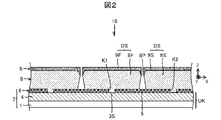
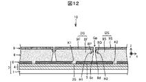
- FIG. 2 is a cross-sectional view showing another configuration of the semiconductor substrate according to this embodiment.
- the semiconductor substrate 10 includes a main substrate 1, an underlying layer 4, a mask pattern 6, first and second semiconductor portions 8F and 8S, and a first functional layer 9F above the first semiconductor portion 8F. and a second functional layer 9S above the second semiconductor portion 8S. overlaps.
- Each of the first and second functional layers 9F and 9S may be a single layer body or a laminate body.
- the first functional layer 9F may have at least one of a function as a component of a semiconductor device, an optical function, and a sensing function.
- the first semiconductor portion 8F has the first projecting portion H1. It becomes difficult for the raw material to reach the mask portion 5 located therebetween, and the formation of deposits is reduced. Further, since the first functional layer 9F formed above the first semiconductor portion 8F is difficult to be formed below the top portion 8P of the first protruding portion H1, the first functional layer 9F and the second functional layer 9S is less likely to be connected.
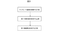
- FIG. 3 is a flow chart showing an example of a method for manufacturing a semiconductor substrate according to this embodiment.
- the step of preparing the template substrate (ELO growth substrate) 7 the step of forming the first semiconductor portion 8F using the ELO method is performed.
- the step of forming the first functional layer 9F can be performed as necessary.
- a mask pattern 6 may be formed on the underlying substrate UK.
- FIG. 4 is a block diagram showing an example of a semiconductor substrate manufacturing apparatus according to this embodiment.
- the semiconductor formation portion 72 has a first lower edge 8c positioned above the mask portion 5 and a first projecting portion H1 projecting in the X direction (a-axis direction) from the first lower edge 8c in plan view.
- 1 Semiconductor portion 8F (see FIG. 1) is formed by the ELO method.
- the semiconductor substrate manufacturing apparatus 70 may be configured to form the first functional layer 9F.
- the semiconductor formation section 72 may include an MOCVD apparatus, and the control section 74 may include a processor and memory.
- the control unit 74 may be configured to control the semiconductor forming unit 72 by executing a program stored in an internal memory, a communicable communication device, or an accessible network.
- This embodiment also includes a recording medium and the like.
- FIG. 5 is a flow chart showing an example of a method for manufacturing a semiconductor device according to this embodiment.
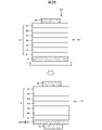
- FIG. 6 is a plan view showing an example of separation of the element portion.
- FIG. 7 is a cross-sectional view showing an example of separation and separation of element portions.
- the step of preparing the semiconductor substrate 10 after the step of preparing the semiconductor substrate 10, the step of forming the first functional layer 9F on the first semiconductor portion 8F is performed as necessary. Thereafter, as shown in FIGS. 6 and 7, a plurality of trenches TR (separation trenches) are formed in the semiconductor substrate 10 to cover the element portion DS (including the low defect portion EK of the first semiconductor portion 8F and the first functional layer 9F). ) is separated.
- trenches TR separation trenches
- Trench TR penetrates through first functional layer 9F and first semiconductor portion 8F.
- Base layer 4 and mask portion 5 may be exposed in trench TR.
- the opening width of trench TR can be equal to or greater than the width of first opening K1.
- the element portion DS is van der Waals coupled with the mask portion 5 and is a part of the semiconductor substrate 10 .
- the element portion DS is separated from the template substrate 7 to form a semiconductor device 20.
- the first functional layer 9F of the isolated element portion DS includes an end face 9x perpendicular to the X direction, but the end face 9x is not eroded by etching, so the first functional layer 9F (especially the active layer) is of good quality. is realized.
- the step of preparing the semiconductor substrate 10 shown in FIG. 5 may include each step of the semiconductor substrate manufacturing method shown in FIG.
- a semiconductor device 20 As shown in FIG. 7, by separating the element portion DS from the template substrate 7, a semiconductor device 20 (including, for example, a GaN-based crystal) can be formed. As a separation method, the semiconductor device 20 may be bonded to another carrier substrate using solder, or may be made using a flexible material such as an adhesive material or silicone elastomer polydimethylsiloxane (PDMS). It may be peeled off using an adhesive stamp.
- PDMS silicone elastomer polydimethylsiloxane
- semiconductor device 20 include light emitting diodes (LEDs), semiconductor lasers, Schottky diodes, photodiodes, transistors (including power transistors and high electron mobility transistors), and the like.
- LEDs light emitting diodes
- semiconductor lasers semiconductor lasers
- Schottky diodes Schottky diodes
- photodiodes transistors (including power transistors and high electron mobility transistors), and the like.
- FIG. 8 is a schematic diagram showing the configuration of the electronic device according to this embodiment.
- the electronic device 30 of FIG. 8 includes a semiconductor substrate 10 (a configuration that functions as a semiconductor device while including the template substrate 7, for example, when the template substrate 7 is translucent) and a driving substrate on which the semiconductor substrate 10 is mounted. 23 and a control circuit 25 that controls the drive board 23 .
- FIG. 9 is a schematic diagram showing another configuration of the electronic device according to this embodiment.
- An electronic device 30 of FIG. 9 includes a semiconductor device 20 including at least a low-defect portion EK, a drive board 23 on which the semiconductor device 20 is mounted, and a control circuit 25 that controls the drive board 23 .
- Examples of the electronic device 30 include a display device, a laser emitting device (including a Fabry-Perot type and a surface emitting type), a lighting device, a communication device, an information processing device, a sensing device, a power control device, and the like.
- Example 1 (overall structure) 10A and 10B are a plan view and a cross-sectional view showing the configuration of the semiconductor substrate according to the first embodiment.
- a semiconductor substrate 10 according to Example 1 includes a main substrate 1, a base layer 4 positioned above the main substrate 1, and first and second openings K1 and K2 adjacent in the X direction. , and a mask pattern 6 including a mask portion 5 located between the first and second openings K1 and K2, and first and second semiconductor portions 8F and 8S located above the mask pattern 6.
- the first and second semiconductor portions 8F and 8S are formed by the ELO method, are separated from each other, and are adjacent to each other. Note that the first and second semiconductor portions 8F and 8S may be referred to as ELO semiconductor layers 8 in some cases.
- the first and second semiconductor portions 8F and 8S can also be called first and second semiconductor layers.
- the first semiconductor part 8F has a first protruding part H1 that overlaps the first opening K1 in plan view and protrudes in the X direction (toward the second semiconductor part 8S) from the first lower edge 8c.
- the second semiconductor portion 8S overlaps the second opening portion K2 in a plan view, and a second overhang portion H2 overhangs in the opposite direction in the X direction (toward the first semiconductor portion 8F) from the second lower edge 8d.
- the lower edge means for example, the edge of the lower surface of the semiconductor layer portion
- the upper edge means, for example, the edge of the upper surface of the semiconductor layer portion.
- a heterosubstrate having a lattice constant different from that of the GaN-based semiconductor can be used for the main substrate 1 .
- hetero-substrates include single-crystal silicon (Si) substrates, sapphire (Al 2 O 3 ) substrates, silicon carbide (SiC) substrates, and the like.
- the plane orientation of the main substrate 1 is, for example, the (111) plane of a silicon substrate, the (0001) plane of a sapphire substrate, and the 6H—SiC (0001) plane of a SiC substrate. These are just examples, and any main substrate and plane orientation may be used as long as the ELO semiconductor layer 8 can be grown by the ELO method.
- a buffer layer 2 eg, AlN layer
- a seed layer 3 eg, nitride semiconductor
- the buffer layer 2 has a function of reducing, for example, the direct contact between the main substrate 1 and the seed layer 3 and the mutual melting.
- a silicon substrate or the like is used for the main substrate 1, it melts with the GaN-based semiconductor that is the seed layer 3. Therefore, by providing the buffer layer 2 such as an AlN layer, the melting is reduced.
- the main substrate 1 that does not melt together with the seed layer 3, which is a GaN-based semiconductor is used, a configuration without the buffer layer 2 is possible.
- An AlN layer which is an example of the buffer layer 2 can be formed to a thickness of about 10 nm to about 5 ⁇ m using, for example, an MOCVD apparatus.
- the buffer layer 2 may have at least one of the effect of increasing the crystallinity of the seed layer 3 and the effect of relieving the internal stress of the ELO semiconductor layer 8 .
- a GaN-based semiconductor containing Al for example, can be used for the seed layer 3 .
- the seed layer 3 includes a seed portion 3S (growing starting point of the ELO semiconductor layer) overlapping the first opening K1 of the mask pattern 6.
- a graded layer in which the Al composition approaches graded GaN may be used.
- the graded layer is, for example, a laminate in which an Al 0.7 Ga 0.3 N layer as a first layer and an Al 0.3 Ga 0.7 N layer as a second layer are provided in order from the buffer layer side is.
- the graded layer can be easily formed by MOCVD, and may be composed of three or more layers. By using a graded layer for the seed layer 3, the stress from the main substrate 1, which is a different substrate, can be relieved.
- the seed layer 3 can be configured to include a GaN layer. In this case, the seed layer 3 may be a single layer of GaN, or the uppermost layer of the graded layer that is the seed layer 3 may be a GaN layer.
- At least one of the buffer layer 2 (eg, aluminum nitride) and seed layer 3 (eg, GaN-based semiconductor) can also be deposited using a sputtering device (PSD: pulse sputter deposition, PLD: pulse laser deposition, etc.).
- PLD pulse sputter deposition
- PLD pulse laser deposition
- Mask pattern 6 (mask layer) includes mask portion 5 and first and second openings K1 and K2.
- the first and second openings K1 and K2 expose the seed portion 3S and have the function of growth start holes for starting the growth of the ELO semiconductor layer 8.
- the mask portion 5 allows the ELO semiconductor layer 8 to extend laterally. It may have a function of a selective growth mask for growing.
- the first and second openings K ⁇ b>1 and K ⁇ b>2 are portions (non-formation portions) of the mask pattern 6 where the mask portion 5 does not exist, and may not be surrounded by the mask portion 5 .
- SiOx silicon oxide film
- TiN titanium nitride film
- SiNx silicon nitride film
- SiON silicon oxynitride film
- a metal film having a high melting point for example, 1000° C. or higher.
- a single layer film containing any one of or a laminated film containing at least two of these can be used.
- a silicon oxide film having a thickness of about 100 nm to 4 ⁇ m (preferably about 150 nm to 2 ⁇ m) is formed on the underlying layer 4 by sputtering, and a resist is applied to the entire surface of the silicon oxide film.
- the resist is patterned by photolithography to form a resist having a plurality of striped openings.
- a portion of the silicon oxide film is removed by a wet etchant such as hydrofluoric acid (HF) or buffered hydrofluoric acid (BHF) to form a plurality of openings (including K1 and K2), and the resist is removed by organic cleaning.
- a mask pattern 6 is formed.
- the first and second openings K1 and K2 have a longitudinal shape (slit shape) and are periodically arranged in the a-axis direction (X direction) of the ELO semiconductor layer 8 .
- the widths of the first and second openings K1 and K2 are about 0.1 ⁇ m to 20 ⁇ m. As the width of each opening becomes smaller, the number of threading dislocations propagating from each opening into the ELO semiconductor layer 8 decreases. In addition, it becomes easy to separate (separate) the ELO semiconductor layer 8 from the template substrate 7 in a post-process. Furthermore, the area of the low-defect portion EK (for example, GaN-based crystal) with few surface defects can be increased.
- the silicon oxide film decomposes and evaporates in small amounts during the formation of the ELO semiconductor layer 8 and may be taken into the ELO semiconductor layer 8.
- the silicon nitride film and the silicon oxynitride film decompose and evaporate at high temperatures. It has the advantage of being difficult.
- the mask pattern 6 may be a single layer film of a silicon nitride film or a silicon oxynitride film, or may be a laminated film in which a silicon oxide film and a silicon nitride film are formed in this order on the base layer 4.
- 4 may be a laminated film in which a silicon nitride film and a silicon oxide film are formed in this order, or a laminated film in which a silicon nitride film, a silicon oxide film and a silicon nitride film are formed in this order on an underlying layer.
- a good mask pattern 6 can also be formed by using a general silicon oxide film (single layer) and using such a film formation method.
- a laminate was used in which a silicon oxide film (SiO 2 ) and a silicon nitride film (SiN) were formed in this order.
- the thickness of the silicon oxide film is, for example, 0.3 ⁇ m, and the thickness of the silicon nitride film is, for example, 70 nm.
- a plasma-enhanced chemical vapor deposition (CVD) method was used to form each of the silicon oxide film and the silicon nitride film.
- Example 1 (Formation of ELO semiconductor layer)
- the ELO semiconductor layer 8 was a GaN layer, and an ELO film of gallium nitride (GaN) was formed on the template substrate 7 by the MOCVD apparatus included in the semiconductor forming section 72 of FIG.
- substrate temperature 1120° C.
- growth pressure 50 kPa
- TMG trimethylgallium
- NH 3 15 slm
- V/III 6000 supply ratio
- the first and second semiconductor portions 8F and 8S are selectively grown on the seed portion 3S (the GaN layer which is the uppermost layer of the seed layer 3) exposed in the first and second openings K1 and K2. It grows laterally on the mask portion 5 . Then, the lateral growth of the first and second semiconductor portions 8F and 8S laterally grown from both sides on the mask portion 5 is stopped before they meet. Before the growth of the first and second semiconductor parts 8F and 8S is stopped, the lower inclined surface EC expands its area in an overhanging state without substantially changing the lower space Pc in FIG. A period may be included.
- the width Wm of the mask portion 5 is 50 ⁇ m
- the width of the first and second openings K1 and K2 is 5 ⁇ m
- the lateral width of the ELO semiconductor layer 8 is 53 ⁇ m
- the width (size in the X direction) of the low defect portion EK is 24 ⁇ m
- the ELO semiconductor The layer thickness of layer 8 was 5 ⁇ m.
- the ELO semiconductor layer 8 it is preferable to reduce mutual reaction between the ELO semiconductor layer 8 and the mask portion 5 so that the ELO semiconductor layer 8 and the mask portion 5 are brought into contact with each other by Van der Waals force.
- the lateral film formation rate is increased.
- a technique for increasing the lateral film formation rate is as follows. First, a vertical growth layer growing in the Z direction (c-axis direction) is formed on the seed portion 3S exposed from the first and second openings K1 and K2, and then grown in the X direction (a-axis direction). Form a lateral growth layer. At this time, by setting the thickness of the vertical growth layer to 10 ⁇ m or less, 5 ⁇ m or less, 3 ⁇ m or less, or 1 ⁇ m or less, the thickness of the horizontal growth layer can be kept low and the horizontal film formation rate can be increased.
- FIG. 11 is a cross-sectional view showing an example of lateral growth of an ELO semiconductor layer.
- an initial growth layer (part of the dislocation inheriting portion NS) SL is formed on the seed portion 3S, and then the first and second semiconductor portions 8F and 8S are grown laterally from the initial growth layer SL. It is desirable to grow The initial growth layer SL serves as a starting point for lateral growth of the first and second semiconductor portions 8F and 8S.
- the ELO film formation conditions it is possible to control the growth of the first and second semiconductor portions 8F and 8S in the Z direction (c-axis direction) or in the X direction (a-axis direction). be.
- the shape of the first and second overhangs H1 and H2 in FIG. 10 can also be controlled by the ELO film formation conditions (X-direction growth conditions).
- the edge of the initial growth layer SL is immediately before it rises on the upper surface of the mask portion 5 (at the stage when it is in contact with the upper end of the side surface of the mask portion 5), or 5 (that is, at this timing, the ELO film formation conditions are switched from the c-axis direction film formation conditions to the a-axis direction film formation conditions).
- the film formation in the lateral direction proceeds from the state where the initial growth layer SL slightly protrudes from the mask portion 5, so the material consumed for the growth in the thickness direction is reduced, and the first and second semiconductor portions 8F are formed.
- - 8S can be grown laterally at high speed.
- the initial growth layer SL can be formed with a thickness of 50 nm to 5.0 ⁇ m (eg, 80 nm to 2 ⁇ m).
- the thickness of the mask portion 5 and the thickness of the initial growth layer SL may be 500 nm or less.
- the initial growth layer SL is formed and then laterally grown to increase non-threading dislocations inside the low-defect portion EK (low-defect It is possible to reduce the threading dislocation density on the part EK surface. In addition, it is possible to control the distribution of impurity concentration (for example, silicon, oxygen) inside the low-defect portion EK.
- impurity concentration for example, silicon, oxygen
- the ratio of the width (WL) of the first semiconductor portion 8F to the width of the first opening K1 is 3.5 or more, 5.0 or more, 6.0 or more, 8.0. 10 or more, 15 or more, 20 or more, 30 or more, or 50 or more, and the ratio of low defect portions EK increases.
- the first and second semiconductor portions 8F and 8S shown in FIG. 11 can be nitride semiconductor crystals (for example, GaN crystals, AlGaN crystals, InGaN crystals, or InAlGaN crystals).
- the thickness of the vertical growth layer (initial growth layer) is set to 2 ⁇ m or more and the film formation is completed before the films growing laterally on the mask portion 5 meet each other, the thickness of the vertical growth layer It becomes difficult to supply the Ga raw material and the ammonia raw material to the gap portion, and the growth of the ELO semiconductor layer 8 under the end surface can be suppressed.
- the film is formed at a high temperature (for example, a film forming temperature of 1050° C. or higher) and a high V/III (>5000), a reverse tapered crystal face can be easily obtained.
- a temperature of 1150°C or less is preferable to a temperature exceeding 1200°C. It is possible to form the ELO semiconductor layer 8 even at a low temperature of less than 1000° C., which is preferable from the viewpoint of reducing mutual reaction.
- TMG trimethylgallium
- the raw material is not sufficiently decomposed, and gallium atoms and carbon atoms are simultaneously incorporated into the ELO semiconductor layer 8 in a larger amount than usual. rice field.
- film formation in the a-axis direction is fast and film formation in the c-axis direction is slow.
- the carbon incorporated into the ELO semiconductor layer 8 reduces the reaction with the mask portion 5 and reduces adhesion between the mask portion 5 and the ELO semiconductor layer 8. Therefore, when the ELO semiconductor layer 8 is deposited at a low temperature, the amount of ammonia supplied is reduced and the film is deposited at a low V/III ( ⁇ 1000), so that the carbon element in the raw material or the chamber atmosphere is taken into the ELO semiconductor layer 8. , the reaction with the mask portion 5 can be reduced.
- the ELO semiconductor layers (first and second semiconductor portions 8F and 8S) contain carbon.
- the first semiconductor portion 8F includes a first upper edge 8a located between the mask portion center 5c and the first opening K1 in plan view, and a mask portion center 5c in plan view.
- the second semiconductor portion 8S includes a second upper edge 8b positioned between the mask portion center 5c and the second opening K2 in plan view, and a portion between the mask portion center 5c and the second opening K2 in plan view.
- the second lower edge 8d located (located on the mask portion 5) and the second protruding portion H2 protruding in the X direction (first semiconductor portion 8F side) from the second lower edge 8d in plan view. have.
- the portion overlapping the mask portion 5 in plan view contains a GaN-based semiconductor and has an upper surface 8J and a lower surface 8U parallel to the (0001) plane (c-plane).
- GaN-based crystal GK has a non-threading dislocation density in a cross section parallel to the ⁇ 0001> direction higher than a threading dislocation density in the top surface 8J, and has a lower edge 8c parallel to the ⁇ 1-100> direction and a lower edge ⁇ 1-100> than the lower edge. 11-20> direction and an overhang portion (overhang portion) H1.
- the non-threading dislocation density of the GaN-based crystal GK can be 10 times or more, for example, 20 times or more the threading dislocation density.
- the threading dislocation density can be, for example, 5 ⁇ 10 6 [dislocations/cm 2 ] or less.
- the width (size in the X direction) of the GaN-based crystal body GK can be set to, for example, 10 ⁇ m or more. In the GaN-based crystal GK, while suppressing threading dislocations that affect the characteristics of semiconductor devices, non-threading dislocations, which have almost no effect, are present, which has the effect of relieving film stress.
- the non-penetrating dislocation density in the cross section parallel to the (11-20) plane (a-plane) was It may be larger than the dislocation density. Since the GaN-based crystal body GK is formed by growing in the lateral direction (X direction), impurities ( The concentration of atoms contained in the mask pattern 6, such as silicon and oxygen, can be low.
- Example 1 the maximum distance L1 between the first opening K1 and the first projecting portion H1 in the X direction is greater than the distance La between the first opening K1 and the first upper edge 8a. , the maximum distance L2 between the second opening K2 and the second protrusion H2 is greater than the distance Lb between the second opening K2 and the second upper edge 8b.
- the side surface ES of the first semiconductor part includes a lower inclined surface EC including the first lower edge 8c and an upper inclined surface EA including the first upper edge 8a, and is perpendicular to the lower inclined surface EC and the X direction.
- a first acute angle ⁇ 1 formed with the surface VF is smaller than a second acute angle ⁇ 2 formed between the upper inclined surface EA and the surface VF perpendicular to the X direction.
- the first acute angle ⁇ 1 may be 30° or less, 20° or less, or 15° or less.
- a distance Hp between the mask portion 5 and the top portion 8P of the first projecting portion is larger than half the thickness d1 of the first semiconductor portion 8F.
- the second acute angle ⁇ 2 may be 75° or more, 80° or more, or 85° or more.
- the minimum distance Px between the first semiconductor part 8F and the second semiconductor part 8S is the lower distance Pc indicating the distance between the first lower edge 8c and the second lower edge 8d, and the first upper edge 8a and the second upper edge 8b, which is smaller than the upper spacing Pa, and the upper spacing Pa is greater than the lower spacing Pc.
- the minimum spacing Px is, for example, 5 ⁇ m or less
- the lower spacing Pc is, for example, 7 ⁇ m or less
- the upper spacing Pa is, for example, 8 ⁇ m or less.
- the lower space Pc may be smaller than the opening widths of the first and second openings K1 and K2.
- the minimum spacing Px may be smaller than the opening widths of the first and second openings K1 and K2.
- the internal stress of the ELO semiconductor layer 8 is reduced, and cracks and defects occurring in the ELO semiconductor layer 8 are reduced. can be reduced. This effect is particularly great when the main substrate 1 is a different substrate.
- FIG. 12 is a cross-sectional view showing another configuration of the semiconductor substrate according to Example 1.
- the first functional layer 9F is arranged on the first semiconductor section 8F
- the second functional layer 9S is arranged on the second semiconductor section 8S.
- the functional layers 9 are, for example, n-type semiconductor layers (eg, GaN-based), non-doped semiconductor layers (eg, GaN-based), p-type semiconductor layers (eg, GaN-based). system), a conductive layer, and an insulating layer.
- a non-doped semiconductor layer can also be used as an active layer (a layer in which electrons and holes combine).
- the functional layer 9 may be formed by any method.
- first projecting portion H1 is formed in the first semiconductor portion 8F and the second projecting portion H2 is formed in the second semiconductor portion 8S, when forming the first and second functional layers 9F and 9S, It becomes difficult for the raw materials (aluminum source, indium source) and the like to reach the mask portion 5 located between the first and second semiconductor portions 8F and 8S, and the formation of deposits is reduced. It is also possible to prevent the functional layers 9F and 9S from connecting to each other.
- the first functional layer 9F formed above the first semiconductor portion 8F is less likely to be formed below the top portion 8P of the first protruding portion H1, and is located above the second semiconductor portion 8S. Since the second functional layer 9S, which is formed on the upper layer, is less likely to be formed below the top portion 8Q of the second projecting portion H2, the first and second functional layers 9F and 9S are naturally separated during formation ( self-isolation). This improves the yield of the step of isolating the element portion DS.
- the active layer included in the first functional layer 9F has a shape that does not reach the first lower edge 8c
- the active layer included in the second functional layer 9S has a shape that does not reach the second lower edge 8d.
- a GaN-based p-type semiconductor layer for example, is formed in the functional layer 9, silicon and oxygen separated from the silicon-based mask pattern 6 (eg, silicon oxide film) are taken in to form a p-type dopant (eg, Mg). You may be compensated. If the ELO semiconductor layer 8 is a GaN-based n-type semiconductor, silicon or the like may separate from the ELO semiconductor layer 8 as well. In Example 1, the rise of the n-type dopant such as silicon is inhibited by the first and second protrusions H1 and H2. function can be enhanced.
- the first functional layer 9F includes a layer containing indium as a composition (for example, an In x Ga (1-x) N layer, where x is a positive number equal to or less than 1)
- In atoms are larger than Ga atoms.
- crystal defects and in-film stress may occur. , the stress in the film can be relaxed.
- the first functional layer 9F includes a layer containing aluminum as a composition (for example, an Al x Ga (1-x) N layer, where x is a positive number equal to or less than 1)
- a layer containing aluminum as a composition for example, an Al x Ga (1-x) N layer, where x is a positive number equal to or less than 1
- the Al composition increases, the ELO Due to lattice mismatch with the semiconductor layer 8, difference in thermal expansion coefficient, etc., crystal defects such as cracks, crystal slips on crystal planes (for example, m-plane slips in GnN-based semiconductor layers), and intra-film stress
- the first functional layer 9F by separating the first functional layer 9F from the other functional layers, propagation of crystal defects can be suppressed and intra-film stress can be alleviated.
- FIG. 13 is a cross-sectional view showing another configuration of the semiconductor substrate according to this embodiment.
- an edge growth 9G (corner) may occur as shown in FIG.
- the functional layer 9 includes an AlGaN layer.
- Edge growth can have a width of 10 ⁇ m or more and a size of about 200 to 300 nm in height, which hinders post-processes. 9G can be significantly reduced (for example, the height is 100 nm or less).
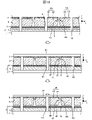
- FIG. 14A and 14B are plan views showing the process of separating the element portion in the first embodiment.
- 15A and 15B are cross-sectional views showing a step of isolating the element portions in the first embodiment.
- dry etching is used to form a plurality of trenches TR extending in the X direction to separate the element portions DS.
- the element portion DS is surrounded by two trenches TR and two gaps Gp extending in the Y direction, and the element portion DS larger than that in FIG. 6 can be separated. Dry etching is realized by a general photolithography method.
- the semiconductor substrate 10 is immersed in an etchant ET to dissolve the mask pattern 6, and then the surface of the ELO semiconductor layer 8 is covered with an adhesive tape (for example, a semiconductor wafer is diced).
- a Peltier element (not shown) may be used to lower the temperature of the semiconductor substrate 10 with the adhesive tape attached thereto.
- the adhesive tape which generally has a larger coefficient of thermal expansion than the semiconductor, shrinks greatly, and stress is applied to the ELO semiconductor layer 8 . Since the ELO semiconductor layer 8 is bonded only to the underlying layer 4 (seed portion) of the template substrate 7 and the mask portion 5 is removed, the stress from the adhesive tape is applied to the underlying layer (of the template substrate 7). 4 and can mechanically cleave or break the bond. That is, it is not necessary to etch away the joint.
- FIG. 16 is a cross-sectional view showing another configuration of the semiconductor substrate of Example 1.
- the semiconductor substrate 10 of FIG. 10 has dislocation inheriting portions NS (portions overlapping the first and second openings K1 and K2 in plan view) of the first and second semiconductor portions 8F and 8S. can also be removed. Further, it is also possible to remove portions of the base layer 4 that overlap the first and second openings K1 and K2 in plan view.
- FIG. 17 is a cross-sectional view showing another configuration of the semiconductor substrate 10 of Example 1.
- first and second functional layers 9F and 9S can also be provided on the first and second semiconductor portions 8F and 8S in FIG.
- FIG. 18 is a cross-sectional view showing another step of separating the element portions in Example 1.
- FIG. Since the ELO semiconductor layer 8 and the mask portion 5 in FIG. 17 are coupled by van der Waals force (weak force), as shown in FIG. etc.), the element portion DS can be easily peeled off from the template substrate, and the semiconductor device 20 can be obtained. Being able to peel off directly from the mask portion 5 using a viscoelastic elastomer stamp, an electrostatic adhesive stamp, or the like is a great advantage in terms of cost, throughput, and the like. After contacting the ELO semiconductor layer 8 with a viscoelastic elastomer stamp, an electrostatic adhesive stamp, or the like, for example, ultrasonic vibrations or the like may be applied. By this vibration or the like, the ELO semiconductor layer 8 can be peeled off from the mask portion 5 more easily.
- FIG. 19 is a cross-sectional view showing the configuration of the semiconductor substrate of Example 2.
- the first semiconductor portion 8F includes a first upper edge 8a positioned between the mask portion center 5c and the first opening K1 in plan view, and a first upper edge 8a positioned between the mask portion center 5c and the first opening K1 in plan view.
- a first lower edge 8c located on the mask portion 5) located between the first opening K1 and projecting in the X direction (toward the second semiconductor portion 8S) from the first lower edge 8c in plan view. and a first projecting portion H1.
- the second semiconductor portion 8S includes a second upper edge 8b positioned between the mask portion center 5c and the second opening K2 in plan view, and a portion between the mask portion center 5c and the second opening K2 in plan view.
- the second lower edge 8d located (located on the mask portion 5) and the second protruding portion H2 protruding in the X direction (first semiconductor portion 8F side) from the second lower edge 8d in plan view. have.
- the portion overlapping the mask portion 5 in plan view contains a GaN-based semiconductor and has an upper surface 8J and a lower surface 8U parallel to the (0001) plane (c-plane).
- GaN-based crystal GK has a non-threading dislocation density in a cross section parallel to the ⁇ 0001> direction higher than a threading dislocation density in the top surface 8J, and has a lower edge 8c parallel to the ⁇ 1-100> direction and a lower edge ⁇ 1-100> than the lower edge. 11-20> direction and an overhang portion (overhang portion) H1.
- the first upper edge 8a is the top of the first projecting portion H1
- the second upper edge 8b is the top of the second projecting portion H2.
- the distance La between the first opening K1 and the first upper edge 8a is greater than the distance Lc between the first opening K1 and the first lower edge 8c
- the second opening K2 and the second upper edge 8a are separated from each other.
- a distance Lb to the edge 8b is greater than a distance Ld between the second opening K2 and the second lower edge 8d.
- a gap Gp sandwiched between the first semiconductor portion 8F and the second semiconductor portion 8S has an inverse tapered shape that is wider on the mask portion 5 side.
- the upper spacing Pa indicating the spacing between the first upper edge 8a and the second upper edge 8b is smaller than 5 ⁇ m.
- the ratio of the upper spacing Pa to the width Wm of the mask portion is less than 0.5
- the ratio of the lower spacing Pc indicating the spacing between the first lower edge 8c and the second lower edge 8d to the width Wm of the mask portion is 0. less than .7.
- An acute angle ⁇ formed between a plane EF including the first upper edge 8a and the first lower edge 8c and a plane VF perpendicular to the X direction is 15° or less.
- FIG. 20 is a cross-sectional view showing another configuration of the semiconductor substrate according to the second embodiment.
- the first functional layer 9F is arranged on the first semiconductor section 8F
- the second functional layer 9S is arranged on the second semiconductor section 8S.
- the first functional layer 9F formed above the first semiconductor portion 8F is less likely to be formed below the top portion 8P of the first protruding portion H1 and is formed above the second semiconductor portion 8S. Since it is difficult to form the second functional layer 9S below the top portion 8Q of the second projecting portion H2, the first and second functional layers 9F and 9S are separated from each other. This improves the yield of the step of isolating the element portion DS.
- the rise of an n-type dopant such as silicon is greatly reduced by the first and second protrusions H1 and H2. It becomes difficult for the n-type dopant to be incorporated into the p-type semiconductor layer, and the function of the p-type semiconductor layer can be enhanced.
- FIG. 21 is a cross-sectional view showing another configuration of the semiconductor substrate of Example 2.
- the first semiconductor portion 8F includes a first upper edge 8a positioned between the mask portion center 5c and the first opening K1 in plan view, and a first upper edge 8a positioned between the mask portion center 5c and the first opening K1 in plan view, and a mask portion center 5c and the first opening K1 in plan view.
- a first lower edge 8c located on the mask portion 5) located between the first opening K1 and projecting in the X direction (toward the second semiconductor portion 8S) from the first lower edge 8c in plan view. and a first projecting portion H1.
- the second semiconductor portion 8S includes a second upper edge 8b positioned between the mask portion center 5c and the second opening K2 in plan view, and a portion between the mask portion center 5c and the second opening K2 in plan view.
- the second lower edge 8d located (located on the mask portion 5) and the second protruding portion H2 protruding in the X direction (first semiconductor portion 8F side) from the second lower edge 8d in plan view. have.
- the portion overlapping the mask portion 5 in plan view contains a GaN-based semiconductor and has an upper surface 8J and a lower surface 8U parallel to the (0001) plane (c-plane).
- GaN-based crystal GK has a non-threading dislocation density in a cross section parallel to the ⁇ 0001> direction higher than a threading dislocation density in the top surface 8J, and has a lower edge 8c parallel to the ⁇ 1-100> direction and a lower edge ⁇ 1-100> than the lower edge. 11-20> direction and an overhang portion (overhang portion) H1.
- the side surface ES (end surface) of the first semiconductor portion includes an upper inclined surface EA including the first upper edge 8a, a vertical surface EJ perpendicular to the X direction, and a first lower edge 8c. and a lower inclined plane EC.
- FIG. 22 is a cross-sectional view showing another configuration of the semiconductor substrate of Example 2.
- first and second functional layers 9F and 9S can also be provided on the first and second semiconductor portions 8F and 8S in FIG.
- the ELO semiconductor layer 8 is a GaN layer, but it is not limited to this.
- an InGaN layer which is a GaN-based semiconductor layer, can be formed. Lateral deposition of the InGaN layer is performed at low temperatures, eg, below 1000.degree. This is because, at high temperatures, the vapor pressure of indium increases and it is not effectively incorporated into the film. Lowering the film formation temperature has the effect of reducing the mutual reaction between the mask portion 5 and the InGaN layer. In addition, the InGaN layer has the effect of being less reactive with the mask portion 5 than the GaN layer.
- TAG triethylgallium
- FIG. 23 is a schematic cross-sectional view showing the configuration of Example 4.
- a functional layer 9 forming an LED is formed on the ELO semiconductor layer 8 .
- the ELO semiconductor layer 8 is of n-type doped with silicon or the like, for example.
- the functional layer 9 includes an active layer 34, an electron blocking layer 35, and a GaN-based p-type semiconductor layer 36 in order from the lower layer side.
- the active layer 34 is an MQW (Multi-Quantum Well) and includes an InGaN layer and a GaN layer.
- the electron blocking layer 35 is, for example, an AlGaN layer.
- the GaN-based p-type semiconductor layer 36 is, for example, a GaN layer.
- the anode 38 is arranged in contact with the GaN-based p-type semiconductor layer 36 and the cathode 39 is arranged in contact with the semiconductor layer 8 .
- a semiconductor device 20 including a GaN-based crystal
- films up to the ELO semiconductor layer 8 remove the semiconductor substrate 10 from the film forming apparatus, and then form the functional layer 9 using another apparatus.
- an n-type GaN layer may be inserted between the ELO semiconductor layer 8 and the functional layer 9 as an intermediate layer that serves as a buffer during regrowth.
- the thickness of the intermediate layer can be about 0.1 ⁇ m to about 3 ⁇ m.
- FIG. 24 is a cross-sectional view showing an example of application of the fourth embodiment to electronic equipment.
- a red micro-LED 20R, a green micro-LED 20G, and a blue micro-LED 20B can be obtained, and by mounting these on a drive substrate (TFT substrate) 23, a micro LED display 30D (electronic device) can be configured. can be done.
- a red micro-LED 20R, a green micro-LED 20G, and a blue micro-LED 20B are mounted on a plurality of pixel circuits 27 of the driving substrate 23 via a conductive resin 24 (for example, an anisotropic conductive resin) or the like, and then mounted on the driving substrate 23.
- a control circuit 25, a driver circuit 29, and the like are mounted.
- a portion of the driver circuit 29 may be included in the drive substrate 23 .
- Example 5 is a schematic cross-sectional view showing the configuration of Example 5.
- a functional layer 9 forming a semiconductor laser is formed on the ELO semiconductor layer 8 .
- the functional layer 9 includes, from the lower layer side, an n-type clad layer 41, an n-type guide layer 42, an active layer 43, an electron blocking layer 44, a p-type guide layer 45, a p-type clad layer 46, and a GaN-based p-type semiconductor layer. 47 included.
- An InGaN layer can be used for each of the guide layers 42 and 45 .
- a GaN layer or an AlGaN layer can be used for each of the clad layers 41 and 46 .
- the anode 48 is placed in contact with the GaN-based p-type semiconductor layer 47 and the cathode 49 is placed in contact with the ELO semiconductor layer 8 .
- a semiconductor device 20 including a GaN-based crystal
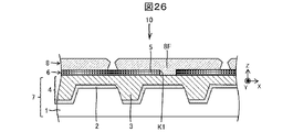
- FIG. 26 is a cross-sectional view showing the configuration of the sixth embodiment.
- a sapphire substrate having an uneven surface is used as the main substrate 1 .
- Underlayer 4 has buffer layer 2 and seed layer 3 .
- a GaN layer having a (20-21) plane is formed as the underlying layer 4 on the main substrate 1 .
- the ELO semiconductor layer 8 has the (20-21) plane, which is the main crystal plane, in the underlying layer 4, and the ELO semiconductor layer 8 having a semipolar plane can be obtained.
- a GaN layer having a (11-22) plane can also be formed as the base layer 4 on the main substrate 1 by using a sapphire substrate having an uneven surface.
- the underlying layer 4 may not be formed over the entire substrate. If the underlying layer 4 contains a material different from that of the main substrate 1, stress may be generated in the semiconductor substrate (ELO semiconductor layer, functional layer) due to differences in thermal expansion coefficient, lattice constant, and the like. Therefore, the underlying layer 4 (at least one of the buffer layer and the seed layer) may be locally provided so as to overlap each opening of the mask pattern 6 . A configuration in which the underlying layer 4 is not provided is also possible.
- FIG. 27 is a cross-sectional view showing the configuration of Embodiment 7.
- the template substrate (ELO growth substrate) 7 may be configured as shown in FIG. 27, for example.
- the template substrate 7 may be composed of the main substrate 1 and the mask pattern 6 (no underlying layer is provided), and the portion of the surface layer of the main substrate 1 overlapping the first opening K1 may function as a seed portion.
- the main substrate 1 a GaN bulk substrate, a 6H--SiC bulk substrate, or a 4H--SiC bulk substrate can be used as the main substrate 1.
- a bulk substrate is a wafer (free-standing substrate) cut from a bulk crystal.
- the template substrate 7 can be composed of the main substrate 1, the seed layer 3 (seed portion) locally arranged so as to overlap the first opening K1 in plan view, and the mask pattern 6.
- the main substrate 1 may be a silicon substrate and the seed layer 3 may contain AlN, or the main substrate 1 may be a silicon carbide substrate and the seed layer 3 may contain a GaN-based semiconductor.
- the template substrate 7 includes the main substrate 1, the buffer layer 2 covering the main substrate 1, the seed layer 3 (seed portion) locally arranged so as to overlap the first opening K1 in plan view, and the mask.
- Pattern 6 can be used.
- the main substrate 1 may be a silicon substrate
- the buffer layer 2 may contain at least one of AlN and SiC
- the seed layer 3 may contain a GaN-based semiconductor.
- the template substrate 7 is composed of the main substrate 1, the buffer layer 2 (buffer portion) locally arranged so as to overlap the first opening K1 in plan view, and the template substrate 7 so as to overlap the first opening K1 in plan view. It can be composed of a seed layer 3 (seed portion) and a mask pattern 6 which are locally arranged in the region.
- the main substrate 1 may be a silicon substrate
- the buffer layer 2 may contain at least one of AlN and silicon carbide
- the seed layer 3 may contain a GaN-based semiconductor.
Abstract
Description
図1は、本実施形態に係る半導体基板の構成を示す平面図および断面図である。本実施形態に係る半導体基板10(半導体ウエハー)は、図1に示すように、主基板1(上面近傍のみ図示)と、主基板1よりも上方に位置し、マスク部5を含むマスクパターン6と、マスクパターン6よりも上層に位置し、隣り合った第1半導体部8Fおよび第2半導体部8Sとを備え、第1半導体部8Fは、マスク部5上に位置する第1下方エッジ8cと、平面視において第1下方エッジ8cよりも第2半導体部8S側に張り出した第1張出部H1とを有している。マスクパターン6は、第1方向(以下、X方向)に隣り合う第1開口部K1および第2開口部K2と、第1開口部K1および第2開口部K2の間に位置するマスク部5とを含む構成とすることができる。 [Semiconductor substrate]
1A and 1B are a plan view and a cross-sectional view showing the configuration of a semiconductor substrate according to this embodiment. A semiconductor substrate 10 (semiconductor wafer) according to the present embodiment includes, as shown in FIG. , and a
図3は、本実施形態にかかる半導体基板の製造方法の一例を示すフローチャートである。図3の半導体基板の製造方法では、テンプレート基板(ELO成長用基板)7を準備する工程の後に、ELO法を用いて第1半導体部8Fを形成する工程を行う。第1半導体部8Fを形成する工程の後に、必要に応じて、第1機能層9Fを形成する工程を行うことができる。テンプレート基板7を準備する工程では、下地基板UK上にマスクパターン6を形成してもよい。 [Manufacture of semiconductor substrates]
FIG. 3 is a flow chart showing an example of a method for manufacturing a semiconductor substrate according to this embodiment. In the method of manufacturing the semiconductor substrate of FIG. 3, after the step of preparing the template substrate (ELO growth substrate) 7, the step of forming the
図5は、本実施形態にかかる半導体デバイスの製造方法の一例を示すフローチャートである。図6は、素子部の分離の一例を示す平面図である。図7は、素子部の分離および離隔の一例を示す断面図である。図5の半導体デバイスの製造方法では、半導体基板10を準備する工程の後に、必要に応じて、第1半導体部8F上に第1機能層9Fを形成する工程を行う。その後、図6および図7に示すように、半導体基板10に複数のトレンチTR(分離溝)を形成して素子部DS(第1半導体部8Fの低欠陥部EKおよび第1機能層9Fを含む)を分離する工程を行う。トレンチTRは、第1機能層9Fおよび第1半導体部8Fを貫通する。トレンチTR内に下地層4およびマスク部5が露出してもよい。トレンチTRの開口幅は、第1開口部K1の幅以上とすることができる。この段階では、素子部DSはマスク部5とファンデルワールス結合しており、半導体基板10の一部である。 [Manufacture of semiconductor devices]
FIG. 5 is a flow chart showing an example of a method for manufacturing a semiconductor device according to this embodiment. FIG. 6 is a plan view showing an example of separation of the element portion. FIG. 7 is a cross-sectional view showing an example of separation and separation of element portions. In the manufacturing method of the semiconductor device of FIG. 5, after the step of preparing the
図7に示すように、素子部DSをテンプレート基板7から離隔することで、半導体デバイス20(例えば、GaN系結晶体を含む)を形成することができる。離隔する方法としては、半田を用いて、別のキャリア基板に半導体デバイス20をボンディングしてもよいし、粘着材あるいはシリコーンエラストマーであるポリジメチルシロキサン(PDMS)等の柔軟材を用いて作製された粘着性スタンプを用いて剥離してもよい。 [Semiconductor device]
As shown in FIG. 7, by separating the element portion DS from the
図8は、本実施形態に係る電子機器の構成を示す模式図である。図8の電子機器30は、半導体基板10(テンプレート基板7を含んだ状態で半導体デバイスとして機能する構成、例えばテンプレート基板7が透光性である場合)と、半導体基板10が実装される駆動基板23と、駆動基板23を制御する制御回路25とを含む。 〔Electronics〕
FIG. 8 is a schematic diagram showing the configuration of the electronic device according to this embodiment. The
(全体構成)
図10は、実施例1に係る半導体基板の構成を示す平面図および断面図である。図10に示すように、実施例1に係る半導体基板10は、主基板1と、主基板1の上方に位置する下地層4と、X方向に隣り合う第1および第2開口部K1・K2、並びに第1および第2開口部K1・K2の間に位置するマスク部5を含むマスクパターン6と、マスクパターン6よりも上層に位置する第1および第2半導体部8F・8Sとを備える。第1および第2半導体部8F・8Sは、ELO法で形成され、互いに分離され、かつ隣り合う。なお、第1および第2半導体部8F・8SをELO半導体層8と称することがある。第1および第2半導体部8F・8Sを、第1および第2半導体層と称することもできる。 [Example 1]
(overall structure)
10A and 10B are a plan view and a cross-sectional view showing the configuration of the semiconductor substrate according to the first embodiment. As shown in FIG. 10, a
主基板1には、GaN系半導体と異なる格子定数を有する異種基板を用いることができる。異種基板としては、単結晶のシリコン(Si)基板、サファイア(Al2O3)基板、シリコンカーバイド(SiC)基板等を挙げることができる。主基板1の面方位は、例えば、シリコン基板の(111)面、サファイア基板の(0001)面、SiC基板の6H-SiC(0001)面である。これらは例示であって、ELO半導体層8をELO法で成長させることができる主基板および面方位であれば何でもよい。 (main board)
A heterosubstrate having a lattice constant different from that of the GaN-based semiconductor can be used for the
下地層4として、主基板側から順に、バッファ層2(例えば、AlN層)およびシード層3(例えば、窒化物半導体)を設けることができる。バッファ層2は、例えば、主基板1とシード層3とがダイレクトに接触して互いに溶融することを低減する機能を有する。主基板1にシリコン基板等を用いた場合、シード層3であるGaN系半導体と溶融し合うため、例えば、AlN層等のバッファ層2を設けることで、溶融が低減される。例えば、GaN系半導体であるシード層3と溶融し合わない主基板1を用いた場合には、バッファ層2を設けない構成も可能である。バッファ層2の一例であるAlN層は、例えばMOCVD装置を用いて、厚さ10nm程度~5μm程度に形成することができる。バッファ層2が、シード層3の結晶性を高める効果、およびELO半導体層8の内部応力を緩和する効果の少なくとも一方を有していてもよい。 (Underlayer)
As the
マスクパターン6(マスク層)は、マスク部5および第1および第2開口部K1・K2を含む。第1および第2開口部K1・K2は、シード部3Sを露出させ、ELO半導体層8の成長を開始させる成長開始用ホールの機能を有し、マスク部5は、ELO半導体層8を横方向成長させる選択成長用マスクの機能を有していてもよい。第1および第2開口部K1・K2は、マスクパターン6におけるマスク部5がない部分(非形成部)であり、マスク部5に囲まれていなくてもよい。 (mask pattern)
Mask pattern 6 (mask layer) includes
主基板1には、(111)面を有するシリコン基板を用い、下地層4のバッファ層2は、AlN層(例えば、30nm)とした。下地層4のシード層3は、第1層であるAl0.6Ga0.4N層(例えば、300nm)と、第2層であるGaN層(例えば、1~2μm)とがこの順に形成されたグレーデット層とする。すなわち、第2層(Ga:N=1:1)におけるGaの組成比(1/2=0.5)は、第1層(Al:Ga:N=0.6:0.4:1)におけるGaの組成比(0.6/2=0.3)よりも大きい。 (Specific example of template substrate)
A silicon substrate having a (111) plane was used as the
実施例1では、ELO半導体層8をGaN層とし、図4の半導体形成部72に含まれるMOCVD装置によってテンプレート基板7上に窒化ガリウム(GaN)のELO成膜を行った。ELO成膜条件の一例として、基板温度:1120℃、成長圧力:50kPa、TMG(トリメチルガリウム):22sccm、NH3:15slm、V/III=6000(III族原料の供給量に対する、V族原料の供給量の比)を採用することができる。 (Formation of ELO semiconductor layer)
In Example 1, the
図10の半導体基板10においては、第1半導体部8Fは、平面視においてマスク部中央5cと第1開口部K1との間に位置する第1上方エッジ8aと、平面視においてマスク部中央5cと第1開口部K1との間に位置する(マスク部5上に位置する)第1下方エッジ8cと、平面視において、第1下方エッジ8cよりもX方向(第2半導体部8S側)に張り出した第1張出部H1とを有する。 (Example of shape of ELO semiconductor layer)
In the
図12は、実施例1に係る半導体基板の別構成を示す断面図である。図12では、第1半導体部8F上に第1機能層9Fが配され、第2半導体部8S上に第2機能層9Sが配される。機能層9(第1および第2機能層9F・9Sを含む)は、例えば、n型半導体層(例えば、GaN系)、ノンドープ半導体層(例えば、GaN系)、p型半導体層(例えば、GaN系)、導電層、および絶縁層の少なくとも1つを含む構成とすることができる。ノンドープ半導体層を活性層(電子と正孔が結合する層)とすることもできる。機能層9は任意の方法で形成すればよい。 (functional layer)
FIG. 12 is a cross-sectional view showing another configuration of the semiconductor substrate according to Example 1. FIG. In FIG. 12, the first
図14は、実施例1における素子部の分離の工程を示す平面図である。図15は、実施例1における素子部の離隔の工程を示す断面図である。実施例1では、図14のように、ドライエッチングを用いてX方向に伸びる複数のトレンチTRを形成し、素子部DSを分離する。平面視では、素子部DSが2つのトレンチTRと、Y方向に伸びる2つのギャップGpとで囲まれており、図6よりも大型の素子部DSを分離することができる。ドライエッチングは、一般的なフォトリソグラフィ法で実現される。エッチング終了後に、エッチング時のマスクであるフォトレジストを除去する必要があるが、例えば弱超音波を用いた有機洗浄を行えば、素子部DSがマスク部5から剥がれ落ちるおそれは少ない。 (Separation and separation of element parts)
14A and 14B are plan views showing the process of separating the element portion in the first embodiment. 15A and 15B are cross-sectional views showing a step of isolating the element portions in the first embodiment. In Example 1, as shown in FIG. 14, dry etching is used to form a plurality of trenches TR extending in the X direction to separate the element portions DS. In plan view, the element portion DS is surrounded by two trenches TR and two gaps Gp extending in the Y direction, and the element portion DS larger than that in FIG. 6 can be separated. Dry etching is realized by a general photolithography method. After the etching is finished, it is necessary to remove the photoresist that is used as a mask during etching. However, organic cleaning using weak ultrasonic waves, for example, reduces the possibility that the element portion DS will come off from the
図16は、実施例1の半導体基板の別構成を示す断面図である。図16に示すように、図10の半導体基板10に対して、第1および第2半導体部8F・8Sの転位継承部NS(平面視で第1および第2開口部K1・K2と重なる部分)を除去することもできる。また、下地層4のうち平面視で第1および第2開口部K1・K2と重なる部分を除去することもできる。図17は、実施例1の半導体基板10の別構成を示す断面図である。図17に示すように、図16の第1および第2半導体部8F・8S上に、第1および第2機能層9F・9Sを設けることもできる。 (Structure from which the dislocation-inheriting part is removed)
16 is a cross-sectional view showing another configuration of the semiconductor substrate of Example 1. FIG. As shown in FIG. 16, the
図19は、実施例2の半導体基板の構成を示す断面図である。図19の半導体基板10では、第1半導体部8Fは、平面視においてマスク部中央5cと第1開口部K1との間に位置する第1上方エッジ8aと、平面視においてマスク部中央5cと第1開口部K1との間に位置する(マスク部5上に位置する)第1下方エッジ8cと、平面視において、第1下方エッジ8cよりもX方向(第2半導体部8S側)に張り出した第1張出部H1とを有する。 [Example 2]
FIG. 19 is a cross-sectional view showing the configuration of the semiconductor substrate of Example 2. FIG. In the
実施例1・2では、ELO半導体層8をGaN層としているがこれに限定されない。実施例1・2のELO半導体層8として、GaN系半導体層であるInGaN層を形成することもできる。InGaN層の横方向成膜は、例えば1000℃を下回るような低温で行う。高温ではインジウムの蒸気圧が高くなり、膜中に有効に取り込まれないためである。成膜温度が低温になることで、マスク部5とInGaN層の相互反応が低減される効果がある。また、InGaN層は、GaN層よりもマスク部5との反応性が低いという効果もある。InGaN層にインジウムがIn組成レベル1%以上で取り込まれるようになると、マスク部5との反応性がさらに低下するため、望ましい。ガリウム原料ガスとしては、トリエチルガリウム(TEG)を用いることが好ましい。 [Example 3]
In Examples 1 and 2, the
図23は、実施例4の構成を示す模式的断面図である。実施例4では、ELO半導体層8上に、LEDを構成する機能層9を成膜する。ELO半導体層8は、例えばシリコン等がドープされたn型である。機能層9は、下層側から順に、活性層34、電子ブロッキング層35、およびGaN系p型半導体層36を含む。活性層34は、MQW(Multi-Quantum Well)であり、InGaN層およびGaN層を含む。電子ブロッキング層35は、例えばAlGaN層である。GaN系p型半導体層36は、例えばGaN層である。アノード38は、GaN系p型半導体層36と接触するように配され、カソード39は、半導体層8と接触するように配される。ELO半導体層8および機能層9をテンプレート基板7から離隔することで半導体デバイス20(GaN系結晶体を含む)を得ることができる。ELO半導体層8まで成膜し、半導体基板10を一旦成膜装置から取り出し、別の装置で機能層9を成膜することもできる。この場合、ELO半導体層8と機能層9との間に、n型のGaN層を再成長の際のバッファとなる中間層として挿入してもよい。中間層の厚さは、0.1μm程度~3μm程度とすることができる。 [Example 4]
FIG. 23 is a schematic cross-sectional view showing the configuration of Example 4. FIG. In Example 4, a
図25は、実施例5の構成を示す模式的断面図である。実施例5では、ELO半導体層8上に、半導体レーザを構成する機能層9を成膜する。機能層9は、下層側から順に、n型クラッド層41、n型ガイド層42、活性層43、電子ブロッキング層44、p型ガイド層45、p型クラッド層46、およびGaN系p型半導体層47を含む。各ガイド層42・45には、InGaN層を用いることができる。各クラッド層41・46には、GaN層もしくはAlGaN層を用いることができる。アノード48はGaN系p型半導体層47と接触するように配され、カソード49はELO半導体層8と接触するように配される。ELO半導体層8および機能層9をテンプレート基板7から離隔することで半導体デバイス20(GaN系結晶体を含む)を得ることができる。 [Example 5]
25 is a schematic cross-sectional view showing the configuration of Example 5. FIG. In Example 5, a
図26は実施例6の構成を示す断面図である。実施例6では、主基板1に、表面凹凸加工されたサファイア基板を用いる。下地層4は、バッファ層2およびシード層3を有する。実施例6では、主基板1上に(20-21)面を持つGaN層を下地層4として成膜する。この場合、ELO半導体層8は下地層4において結晶主面である(20-21)面となり、半極性面のELO半導体層8を得ることができる。半極性面上に、レーザ、LED用の機能層を設けることで、活性層において、電子とホールの再結合確率が高まるといったメリットがある。なお、表面凹凸加工されたサファイア基板を用いることで、主基板1上に(11-22)面をもつGaN層を下地層4として成膜することもできる。 [Example 6]
FIG. 26 is a cross-sectional view showing the configuration of the sixth embodiment. In Example 6, a sapphire substrate having an uneven surface is used as the
下地層4は、基板全体に形成されていなくてもよい。下地層4に主基板1と異なる材料が含まれる場合、熱膨張係数、格子定数等の相異に起因して半導体基板内(ELO半導体層、機能層)に応力を発生させうる。このため、下地層4(バッファ層およびシード層の少なくとも一方)を、マスクパターン6の各開口部と重なるように局所的に設けてもよい。また、下地層4を設けない構成も可能である。 [Example 7]
The
2 バッファ層
3 シード層
3S シード部
4 下地層
5 マスク部
6 マスクパターン
8F 第1半導体部
8S 第2半導体部
9F 第1機能層
9S 第2機能層
10 半導体基板
20 半導体デバイス
30 電子機器
70 半導体基板の製造装置
K1 第1開口部
K2 第2開口部
EK 低欠陥部
GK GaN系結晶体
REFERENCE SIGNS
Claims (37)
- 主基板と、
前記主基板よりも上方に位置し、マスク部を含むマスクパターンと、
前記マスクパターンよりも上方に位置し、隣り合った第1半導体部および第2半導体部とを備え、
前記第1半導体部は、前記マスク部上に位置する第1下方エッジと、前記第1下方エッジよりも前記第2半導体部側へ張り出した第1張出部とを有している、半導体基板。 a main board;
a mask pattern located above the main substrate and including a mask portion;
a first semiconductor portion and a second semiconductor portion located above the mask pattern and adjacent to each other;
The first semiconductor portion has a first lower edge located on the mask portion, and a first protruding portion protruding toward the second semiconductor portion from the first lower edge. . - 前記マスクパターンは、第1方向に隣り合う第1開口部および第2開口部と、前記第1および第2開口部の間に位置する前記マスク部とを含み、
前記第1下方エッジが、平面視において前記マスク部中央と前記第1開口部との間に位置し、
前記第2半導体部が、平面視において前記マスク部中央と前記第2開口部との間に位置する第2下方エッジと、平面視において、前記第2下方エッジよりも前記第1半導体部の側に張り出した第2張出部とを有している、請求項1に記載の半導体基板。 the mask pattern includes a first opening and a second opening adjacent to each other in a first direction, and the mask portion positioned between the first and second openings;
the first lower edge is positioned between the center of the mask portion and the first opening in plan view;
The second semiconductor section has a second lower edge located between the center of the mask section and the second opening in plan view, and a side of the first semiconductor section from the second lower edge in plan view. 2. The semiconductor substrate according to claim 1, further comprising a second overhanging portion that overhangs. - 前記第1半導体部は、平面視において前記マスク部中央と前記第1開口部との間に位置する第1上方エッジを有し、
前記第1方向について、前記第1開口部と前記第1張出部との最大距離が、前記第1開口部と前記第1上方エッジとの距離よりも大きい、請求項2に記載の半導体基板。 The first semiconductor section has a first upper edge located between the center of the mask section and the first opening in plan view,
3. The semiconductor substrate according to claim 2, wherein a maximum distance between said first opening and said first overhang is greater than a distance between said first opening and said first upper edge in said first direction. . - 前記第2半導体部は、平面視において前記マスク部中央と前記第2開口部との間に位置する第2上方エッジを有し、
前記第1方向について、前記第2開口部と前記第2張出部との最大距離が、前記第2開口部と前記第2上方エッジとの距離よりも大きい、請求項3に記載の半導体基板。 The second semiconductor section has a second upper edge located between the center of the mask section and the second opening in plan view,
4. The semiconductor substrate according to claim 3, wherein a maximum distance between said second opening and said second overhang is greater than a distance between said second opening and said second upper edge in said first direction. . - 前記第1半導体部の側面は、前記第1下方エッジを含む下側傾斜面と、前記第1上方エッジを含む上側傾斜面とを含む、請求項3に記載の半導体基板。 4. The semiconductor substrate according to claim 3, wherein the side surface of said first semiconductor portion includes a lower inclined surface including said first lower edge and an upper inclined surface including said first upper edge.
- 前記下側傾斜面と、前記第1方向に垂直な面とがなす第1鋭角は、前記上側傾斜面と前記第1方向に垂直な面とがなす第2鋭角よりも小さい、請求項5に記載の半導体基板。 6. The apparatus according to claim 5, wherein a first acute angle between said lower inclined surface and a surface perpendicular to said first direction is smaller than a second acute angle between said upper inclined surface and a surface perpendicular to said first direction. A semiconductor substrate as described.
- 前記第1鋭角が12°以下である、請求項6に記載の半導体基板。 The semiconductor substrate according to claim 6, wherein said first acute angle is 12° or less.
- 前記マスク部と前記第1張出部の頂部との距離が、前記第1半導体部の厚みの半分よりも大きい、請求項3~7のいずれか1項に記載の半導体基板。 The semiconductor substrate according to any one of claims 3 to 7, wherein the distance between the mask portion and the top portion of the first projecting portion is larger than half the thickness of the first semiconductor portion.
- 前記第1半導体部と前記第2半導体部との最小間隔が、前記第1下方エッジおよび前記第2下方エッジの間隔を示す下側間隔よりも小さい、請求項4に記載の半導体基板。 5. The semiconductor substrate according to claim 4, wherein a minimum distance between said first semiconductor portion and said second semiconductor portion is smaller than a lower distance indicating a distance between said first lower edge and said second lower edge.
- 前記第1半導体部と前記第2半導体部との最小間隔が、前記第1上方エッジおよび前記第2上方エッジの間隔を示す上側間隔よりも小さい、請求項9に記載の半導体基板。 10. The semiconductor substrate according to claim 9, wherein a minimum distance between said first semiconductor portion and said second semiconductor portion is smaller than an upper distance indicating a distance between said first upper edge and said second upper edge.
- 前記上側間隔が前記下側間隔よりも大きい、請求項10に記載の半導体基板。 11. The semiconductor substrate according to claim 10, wherein said upper spacing is greater than said lower spacing.
- 前記第1半導体部は、平面視において前記マスク部中央と前記第1開口部との間に位置する第1上方エッジを有し、
前記第1上方エッジが前記第1張出部の頂部である、請求項2に記載の半導体基板。 The first semiconductor section has a first upper edge located between the center of the mask section and the first opening in plan view,
3. The semiconductor substrate of claim 2, wherein said first upper edge is the top of said first overhang. - 前記第2半導体部は、平面視において前記マスク部中央と前記第2開口部との間に位置する第2上方エッジを有し、
前記第2上方エッジが前記第2張出部の頂部である、請求項12に記載の半導体基板。 The second semiconductor section has a second upper edge located between the center of the mask section and the second opening in plan view,
13. The semiconductor substrate of claim 12, wherein said second upper edge is the top of said second overhang. - 前記第1方向について、前記第1開口部と前記第1上方エッジとの距離が、前記第1開口部と前記第1下方エッジとの距離よりも大きい、請求項13に記載の半導体基板。 14. The semiconductor substrate according to claim 13, wherein a distance between said first opening and said first upper edge is greater than a distance between said first opening and said first lower edge in said first direction.
- 前記第1方向について、前記第2開口部と前記第2上方エッジとの距離が、前記第2開口部と前記第2下方エッジとの距離よりも大きい、請求項14に記載の半導体基板。 15. The semiconductor substrate according to claim 14, wherein a distance between said second opening and said second upper edge is greater than a distance between said second opening and said second lower edge in said first direction.
- 前記第1半導体部と前記第2半導体部とで挟まれた間隙空間は、前記マスク部側が幅広となる逆テーパ形状を有する、請求項15に記載の半導体基板。 16. The semiconductor substrate according to claim 15, wherein a gap space sandwiched between said first semiconductor portion and said second semiconductor portion has an inverse tapered shape with a wider width on the mask portion side.
- 前記第1上方エッジおよび前記第2上方エッジの間隔を示す上側間隔が5μmよりも小さい、請求項13~16のいずれか1項に記載の半導体基板。 The semiconductor substrate according to any one of claims 13 to 16, wherein an upper spacing indicating the spacing between said first upper edge and said second upper edge is smaller than 5 µm.
- 前記第1上方エッジおよび前記第2上方エッジの間隔を示す上側間隔の、前記マスク部の幅に対する比が0.5未満である、請求項13~17のいずれか1項に記載の半導体基板。 18. The semiconductor substrate according to any one of claims 13 to 17, wherein the ratio of the upper spacing indicating the spacing between said first upper edge and said second upper edge to the width of said mask portion is less than 0.5.
- 前記第1下方エッジおよび前記第2下方エッジの間隔を示す下側間隔の、前記マスク部の幅に対する比が0.7未満である、請求項13~18のいずれか1項に記載の半導体基板。 19. The semiconductor substrate according to any one of claims 13 to 18, wherein a ratio of a lower spacing indicating the spacing between said first lower edge and said second lower edge to a width of said mask portion is less than 0.7. .
- 前記第1上方エッジおよび前記第1下方エッジを含む面が、前記第1方向に垂直な面に対して12°以下をなす、請求項13~19のいずれか1項に記載の半導体基板。 The semiconductor substrate according to any one of claims 13 to 19, wherein a plane including said first upper edge and said first lower edge forms an angle of 12° or less with respect to a plane perpendicular to said first direction.
- 前記第1半導体部は、平面視において前記マスク部中央と前記第1開口部との間に位置する第1上方エッジを有し、
前記第1半導体部の側面は、前記第1上方エッジを含む上側傾斜面と、前記第1方向に垂直な垂直面と、前記第1下方エッジを含む下側傾斜面とを含む、請求項2に記載の半導体基板。 The first semiconductor section has a first upper edge located between the center of the mask section and the first opening in plan view,
3. The side surface of the first semiconductor part includes an upper inclined surface including the first upper edge, a vertical surface perpendicular to the first direction, and a lower inclined surface including the first lower edge. The semiconductor substrate according to . - 前記第1半導体部よりも上層に第1機能層が配されている、請求項2~21のいずれか1項に記載の半導体基板。 The semiconductor substrate according to any one of claims 2 to 21, wherein a first functional layer is arranged above the first semiconductor section.
- 前記第1機能層は活性層を含み、
前記活性層が、前記第1下方エッジには至らない、請求項22に記載の半導体基板。 the first functional layer includes an active layer;
23. The semiconductor substrate of claim 22, wherein said active layer does not extend to said first lower edge. - 前記第2半導体部よりも上層に第2機能層が配され、
前記第1機能層と、前記第2機能層とが分離されている請求項22または23に記載の半導体基板。 A second functional layer is arranged above the second semiconductor section,
24. The semiconductor substrate according to claim 22, wherein said first functional layer and said second functional layer are separated. - 前記第1機能層にGaN系のp型半導体層が含まれ、
前記マスクパターンに、シリコン酸化膜およびシリコン窒化膜の少なくとも一方が含まれる、請求項22~24のいずれか1項に記載の半導体基板。 The first functional layer includes a GaN-based p-type semiconductor layer,
25. The semiconductor substrate according to claim 22, wherein said mask pattern includes at least one of a silicon oxide film and a silicon nitride film. - 前記第1および第2開口部は、前記第1方向と直交する第2方向を長手方向とし、
平面視において、前記第1半導体部が前記第1開口部と重なるとともに、前記第2半導体部が前記第2開口部と重なる、請求項2~25のいずれか1項に記載の半導体基板。 The first and second openings have a longitudinal direction in a second direction orthogonal to the first direction,
26. The semiconductor substrate according to claim 2, wherein said first semiconductor portion overlaps said first opening portion and said second semiconductor portion overlaps said second opening portion in plan view. - 前記主基板の上方にシード層が配され、
前記第1半導体部は、前記第1開口部において前記シード層と接する、請求項2~26のいずれか1項に記載の半導体基板。 a seed layer disposed above the main substrate;
27. The semiconductor substrate according to claim 2, wherein said first semiconductor portion is in contact with said seed layer at said first opening. - 前記第1半導体部は、平面視で前記マスク部と重なる低欠陥部を有し、
前記低欠陥部の貫通転位密度が5×10⁶〔個/cm2〕以下であり、
前記低欠陥部の前記第1方向のサイズが10μm以上である、請求項2~27のいずれか1項に記載の半導体基板。 The first semiconductor portion has a low-defect portion overlapping the mask portion in plan view,
The low-defect portion has a threading dislocation density of 5×10 6 pieces/cm 2 or less,
28. The semiconductor substrate according to claim 2, wherein said low-defect portion has a size of 10 μm or more in said first direction. - 前記第1半導体部は、平面視で前記マスク部と重なる低欠陥部を有し、
前記低欠陥部では、厚み方向に平行な断面における非貫通転位密度が上面における貫通転位密度よりも大きい、請求項2~28のいずれか1項に記載の半導体基板。 The first semiconductor portion has a low-defect portion overlapping the mask portion in plan view,
29. The semiconductor substrate according to claim 2, wherein, in said low-defect portion, non-threading dislocation density in a cross section parallel to the thickness direction is higher than threading dislocation density in an upper surface. - 前記第1半導体部が窒化物半導体を含み、前記主基板が、前記窒化物半導体と格子定数が異なる異種基板である、請求項2~29のいずれか1項に記載の半導体基板。 The semiconductor substrate according to any one of claims 2 to 29, wherein the first semiconductor portion contains a nitride semiconductor, and the main substrate is a heterosubstrate having a lattice constant different from that of the nitride semiconductor.
- 前記窒化物半導体がGaNであり、
前記異種基板がシリコン基板であり、
前記第1方向がGaNにおける<11-20>方向である、請求項30に記載の半導体基板。 The nitride semiconductor is GaN,
the hetero-substrate is a silicon substrate,
31. The semiconductor substrate of claim 30, wherein said first direction is the <11-20> direction in GaN. - GaN系半導体を含み、(0001)面に平行な上面および下面を有する、GaN系結晶体であって、
<0001>方向に平行な断面における非貫通転位密度が前記上面における貫通転位密度よりも大きく、
<1-100>方向に平行な下方エッジと、前記下方エッジよりも<11-20>方向に張り出した張出部とを備える、GaN系結晶体。 A GaN-based crystal containing a GaN-based semiconductor and having upper and lower surfaces parallel to the (0001) plane,
The non-threading dislocation density in a cross section parallel to the <0001> direction is higher than the threading dislocation density in the upper surface,
A GaN-based crystal body comprising a lower edge parallel to the <1-100> direction and an overhanging portion extending from the lower edge in the <11-20> direction. - 請求項32に記載のGaN系結晶体を含む、半導体デバイス。 A semiconductor device comprising the GaN-based crystal according to claim 32.
- 請求項1~31のいずれか1項に記載の半導体基板を含む、電子機器。 An electronic device comprising the semiconductor substrate according to any one of claims 1 to 31.
- 請求項33に記載の半導体デバイスを含む、電子機器。 An electronic device comprising the semiconductor device according to claim 33.
- 請求項1~31のいずれか1項に記載の半導体基板の製造方法であって、
前記第1および第2半導体部をELO法によって形成する、半導体基板の製造方法。 A method for manufacturing a semiconductor substrate according to any one of claims 1 to 31,
A method of manufacturing a semiconductor substrate, wherein the first and second semiconductor portions are formed by an ELO method. - 請求項1~31のいずれか1項に記載の半導体基板の製造装置であって、
前記第1および第2半導体部を、ELO法によって形成する半導体形成部と、前記半導体形成部を制御する制御部とを備える半導体基板の製造装置。
The semiconductor substrate manufacturing apparatus according to any one of claims 1 to 31,
An apparatus for manufacturing a semiconductor substrate, comprising: a semiconductor forming section for forming the first and second semiconductor sections by an ELO method; and a control section for controlling the semiconductor forming section.
Priority Applications (2)
| Application Number | Priority Date | Filing Date | Title |
|---|---|---|---|
| JP2023514588A JPWO2022220124A1 (en) | 2021-04-16 | 2022-03-30 | |
| CN202280026769.3A CN117321257A (en) | 2021-04-16 | 2022-03-30 | Semiconductor substrate, method and apparatus for manufacturing the same, gaN-based crystal, semiconductor device, and electronic device |
Applications Claiming Priority (2)
| Application Number | Priority Date | Filing Date | Title |
|---|---|---|---|
| JP2021-069969 | 2021-04-16 | ||
| JP2021069969 | 2021-04-16 |
Publications (1)
| Publication Number | Publication Date |
|---|---|
| WO2022220124A1 true WO2022220124A1 (en) | 2022-10-20 |
Family
ID=83639631
Family Applications (1)
| Application Number | Title | Priority Date | Filing Date |
|---|---|---|---|
| PCT/JP2022/016009 WO2022220124A1 (en) | 2021-04-16 | 2022-03-30 | Semiconductor substrate, manufacturing method and manufacturing apparatus therefor, gan crystal, semiconductor device, and electronic machine |
Country Status (4)
| Country | Link |
|---|---|
| JP (1) | JPWO2022220124A1 (en) |
| CN (1) | CN117321257A (en) |
| TW (1) | TW202309358A (en) |
| WO (1) | WO2022220124A1 (en) |
Citations (2)
| Publication number | Priority date | Publication date | Assignee | Title |
|---|---|---|---|---|
| JP2013532621A (en) * | 2010-06-24 | 2013-08-19 | グロ アーベー | Substrate having a buffer layer for oriented nanowire growth |
| WO2019191760A1 (en) * | 2018-03-30 | 2019-10-03 | The Regents Of The University Of California | Method of fabricating non-polar and semi-polar devices using epitaxial lateral overgrowth |
-
2022
- 2022-03-30 JP JP2023514588A patent/JPWO2022220124A1/ja active Pending
- 2022-03-30 WO PCT/JP2022/016009 patent/WO2022220124A1/en active Application Filing
- 2022-03-30 CN CN202280026769.3A patent/CN117321257A/en active Pending
- 2022-04-15 TW TW111114376A patent/TW202309358A/en unknown
Patent Citations (2)
| Publication number | Priority date | Publication date | Assignee | Title |
|---|---|---|---|---|
| JP2013532621A (en) * | 2010-06-24 | 2013-08-19 | グロ アーベー | Substrate having a buffer layer for oriented nanowire growth |
| WO2019191760A1 (en) * | 2018-03-30 | 2019-10-03 | The Regents Of The University Of California | Method of fabricating non-polar and semi-polar devices using epitaxial lateral overgrowth |
Also Published As
| Publication number | Publication date |
|---|---|
| CN117321257A (en) | 2023-12-29 |
| TW202309358A (en) | 2023-03-01 |
| JPWO2022220124A1 (en) | 2022-10-20 |
Similar Documents
| Publication | Publication Date | Title |
|---|---|---|
| US9171717B2 (en) | Method for manufacturing a group III nitride substrate using a chemical lift-off process | |
| JPH11145516A (en) | Manufacture of gallium nitride compound semiconductor | |
| JP2000323417A (en) | Manufacture for iii group nitride semiconductor and light emitting element thereof | |
| JP2000091253A (en) | Method of producing gallium nitride based compound semiconductor | |
| WO2022181686A1 (en) | Semiconductor substrate, method for producing same, apparatus for producing same, and template substrate | |
| WO2022145454A1 (en) | Semiconductor substrate, semiconductor device and electronic device | |
| WO2022220124A1 (en) | Semiconductor substrate, manufacturing method and manufacturing apparatus therefor, gan crystal, semiconductor device, and electronic machine | |
| JP2000091252A (en) | Gallium nitride based compound semiconductor and semiconductor device | |
| US20240136181A1 (en) | Semiconductor substrate, method for manufacturing the same, apparatus for manufacturing the same, and template substrate | |
| WO2022181584A1 (en) | Template substrate, method and equipment for manufacturing same, semiconductor substrate, and method and equipment for manufacturing same | |
| EP4328956A1 (en) | Semiconductor substrate and production method and production device for same, semiconductor device and production method and production device for same, electronic apparatus | |
| WO2022270309A1 (en) | Semiconductor device manufacturing method and manufacturing device, semiconductor device and electronic device | |
| WO2023027086A1 (en) | Method and device for producing semiconductor device | |
| TWI837788B (en) | Semiconductor device manufacturing method and manufacturing device | |
| WO2023002865A1 (en) | Template substrate and manufacturing method and manufacturing apparatus thereof, semiconductor substrate and manufacturing method and manufacturing apparatus thereof, semiconductor device, and electronic device | |
| WO2024085243A1 (en) | Semiconductor substrate, template substrate, and method and device for producing template substrate | |
| TWI819447B (en) | Semiconductor substrates, semiconductor substrate manufacturing methods, semiconductor substrate manufacturing equipment, electronic components and electronic equipment | |
| WO2023189872A1 (en) | Semiconductor substrate, template substrate, and method and device for producing semiconductor substrate | |
| WO2024084664A1 (en) | Semiconductor substrate, template substrate, and method and device for producing template substrate | |
| TW202205381A (en) | Method for producing semiconductor device, semiconductor device, electronic device, method for producing semiconductor epitaxial substrate, and semiconductor epitaxial substrate |
Legal Events
| Date | Code | Title | Description |
|---|---|---|---|
| 121 | Ep: the epo has been informed by wipo that ep was designated in this application |
Ref document number: 22788049 Country of ref document: EP Kind code of ref document: A1 |
|
| WWE | Wipo information: entry into national phase |
Ref document number: 18555197 Country of ref document: US |
|
| WWE | Wipo information: entry into national phase |
Ref document number: 2023514588 Country of ref document: JP |
|
| NENP | Non-entry into the national phase |
Ref country code: DE |
|
| 122 | Ep: pct application non-entry in european phase |
Ref document number: 22788049 Country of ref document: EP Kind code of ref document: A1 |