WO2022215577A1 - サイドフィル用樹脂組成物、半導体装置、サイドフィル材の除去方法、及び半導体装置の製造方法 - Google Patents
サイドフィル用樹脂組成物、半導体装置、サイドフィル材の除去方法、及び半導体装置の製造方法 Download PDFInfo
- Publication number
- WO2022215577A1 WO2022215577A1 PCT/JP2022/014998 JP2022014998W WO2022215577A1 WO 2022215577 A1 WO2022215577 A1 WO 2022215577A1 JP 2022014998 W JP2022014998 W JP 2022014998W WO 2022215577 A1 WO2022215577 A1 WO 2022215577A1
- Authority
- WO
- WIPO (PCT)
- Prior art keywords
- resin composition
- fill
- base material
- semiconductor device
- component
- Prior art date
- Legal status (The legal status is an assumption and is not a legal conclusion. Google has not performed a legal analysis and makes no representation as to the accuracy of the status listed.)
- Ceased
Links
Images

Classifications
-
- H—ELECTRICITY
- H10—SEMICONDUCTOR DEVICES; ELECTRIC SOLID-STATE DEVICES NOT OTHERWISE PROVIDED FOR
- H10W—GENERIC PACKAGES, INTERCONNECTIONS, CONNECTORS OR OTHER CONSTRUCTIONAL DETAILS OF DEVICES COVERED BY CLASS H10
- H10W74/00—Encapsulations, e.g. protective coatings
- H10W74/10—Encapsulations, e.g. protective coatings characterised by their shape or disposition
- H10W74/131—Encapsulations, e.g. protective coatings characterised by their shape or disposition the semiconductor body being only partially enclosed
- H10W74/141—Encapsulations, e.g. protective coatings characterised by their shape or disposition the semiconductor body being only partially enclosed the encapsulations being on at least the sidewalls of the semiconductor body
-
- C—CHEMISTRY; METALLURGY
- C08—ORGANIC MACROMOLECULAR COMPOUNDS; THEIR PREPARATION OR CHEMICAL WORKING-UP; COMPOSITIONS BASED THEREON
- C08G—MACROMOLECULAR COMPOUNDS OBTAINED OTHERWISE THAN BY REACTIONS ONLY INVOLVING UNSATURATED CARBON-TO-CARBON BONDS
- C08G59/00—Polycondensates containing more than one epoxy group per molecule; Macromolecules obtained by polymerising compounds containing more than one epoxy group per molecule using curing agents or catalysts which react with the epoxy groups
- C08G59/18—Macromolecules obtained by polymerising compounds containing more than one epoxy group per molecule using curing agents or catalysts which react with the epoxy groups ; e.g. general methods of curing
- C08G59/20—Macromolecules obtained by polymerising compounds containing more than one epoxy group per molecule using curing agents or catalysts which react with the epoxy groups ; e.g. general methods of curing characterised by the epoxy compounds used
- C08G59/22—Di-epoxy compounds
- C08G59/226—Mixtures of di-epoxy compounds
-
- C—CHEMISTRY; METALLURGY
- C08—ORGANIC MACROMOLECULAR COMPOUNDS; THEIR PREPARATION OR CHEMICAL WORKING-UP; COMPOSITIONS BASED THEREON
- C08G—MACROMOLECULAR COMPOUNDS OBTAINED OTHERWISE THAN BY REACTIONS ONLY INVOLVING UNSATURATED CARBON-TO-CARBON BONDS
- C08G59/00—Polycondensates containing more than one epoxy group per molecule; Macromolecules obtained by polymerising compounds containing more than one epoxy group per molecule using curing agents or catalysts which react with the epoxy groups
- C08G59/18—Macromolecules obtained by polymerising compounds containing more than one epoxy group per molecule using curing agents or catalysts which react with the epoxy groups ; e.g. general methods of curing
- C08G59/20—Macromolecules obtained by polymerising compounds containing more than one epoxy group per molecule using curing agents or catalysts which react with the epoxy groups ; e.g. general methods of curing characterised by the epoxy compounds used
- C08G59/22—Di-epoxy compounds
- C08G59/24—Di-epoxy compounds carbocyclic
-
- C—CHEMISTRY; METALLURGY
- C08—ORGANIC MACROMOLECULAR COMPOUNDS; THEIR PREPARATION OR CHEMICAL WORKING-UP; COMPOSITIONS BASED THEREON
- C08G—MACROMOLECULAR COMPOUNDS OBTAINED OTHERWISE THAN BY REACTIONS ONLY INVOLVING UNSATURATED CARBON-TO-CARBON BONDS
- C08G59/00—Polycondensates containing more than one epoxy group per molecule; Macromolecules obtained by polymerising compounds containing more than one epoxy group per molecule using curing agents or catalysts which react with the epoxy groups
- C08G59/18—Macromolecules obtained by polymerising compounds containing more than one epoxy group per molecule using curing agents or catalysts which react with the epoxy groups ; e.g. general methods of curing
- C08G59/40—Macromolecules obtained by polymerising compounds containing more than one epoxy group per molecule using curing agents or catalysts which react with the epoxy groups ; e.g. general methods of curing characterised by the curing agents used
- C08G59/42—Polycarboxylic acids; Anhydrides, halides or low molecular weight esters thereof
-
- C—CHEMISTRY; METALLURGY
- C08—ORGANIC MACROMOLECULAR COMPOUNDS; THEIR PREPARATION OR CHEMICAL WORKING-UP; COMPOSITIONS BASED THEREON
- C08G—MACROMOLECULAR COMPOUNDS OBTAINED OTHERWISE THAN BY REACTIONS ONLY INVOLVING UNSATURATED CARBON-TO-CARBON BONDS
- C08G59/00—Polycondensates containing more than one epoxy group per molecule; Macromolecules obtained by polymerising compounds containing more than one epoxy group per molecule using curing agents or catalysts which react with the epoxy groups
- C08G59/18—Macromolecules obtained by polymerising compounds containing more than one epoxy group per molecule using curing agents or catalysts which react with the epoxy groups ; e.g. general methods of curing
- C08G59/40—Macromolecules obtained by polymerising compounds containing more than one epoxy group per molecule using curing agents or catalysts which react with the epoxy groups ; e.g. general methods of curing characterised by the curing agents used
- C08G59/50—Amines
- C08G59/5046—Amines heterocyclic
- C08G59/5053—Amines heterocyclic containing only nitrogen as a heteroatom
- C08G59/5073—Amines heterocyclic containing only nitrogen as a heteroatom having two nitrogen atoms in the ring
-
- C—CHEMISTRY; METALLURGY
- C08—ORGANIC MACROMOLECULAR COMPOUNDS; THEIR PREPARATION OR CHEMICAL WORKING-UP; COMPOSITIONS BASED THEREON
- C08G—MACROMOLECULAR COMPOUNDS OBTAINED OTHERWISE THAN BY REACTIONS ONLY INVOLVING UNSATURATED CARBON-TO-CARBON BONDS
- C08G65/00—Macromolecular compounds obtained by reactions forming an ether link in the main chain of the macromolecule
- C08G65/02—Macromolecular compounds obtained by reactions forming an ether link in the main chain of the macromolecule from cyclic ethers by opening of the heterocyclic ring
- C08G65/04—Macromolecular compounds obtained by reactions forming an ether link in the main chain of the macromolecule from cyclic ethers by opening of the heterocyclic ring from cyclic ethers only
- C08G65/06—Cyclic ethers having no atoms other than carbon and hydrogen outside the ring
- C08G65/16—Cyclic ethers having four or more ring atoms
- C08G65/18—Oxetanes
-
- C—CHEMISTRY; METALLURGY
- C08—ORGANIC MACROMOLECULAR COMPOUNDS; THEIR PREPARATION OR CHEMICAL WORKING-UP; COMPOSITIONS BASED THEREON
- C08K—Use of inorganic or non-macromolecular organic substances as compounding ingredients
- C08K3/00—Use of inorganic substances as compounding ingredients
- C08K3/01—Use of inorganic substances as compounding ingredients characterized by their specific function
- C08K3/013—Fillers, pigments or reinforcing additives
-
- C—CHEMISTRY; METALLURGY
- C08—ORGANIC MACROMOLECULAR COMPOUNDS; THEIR PREPARATION OR CHEMICAL WORKING-UP; COMPOSITIONS BASED THEREON
- C08K—Use of inorganic or non-macromolecular organic substances as compounding ingredients
- C08K3/00—Use of inorganic substances as compounding ingredients
- C08K3/34—Silicon-containing compounds
- C08K3/36—Silica
-
- C—CHEMISTRY; METALLURGY
- C08—ORGANIC MACROMOLECULAR COMPOUNDS; THEIR PREPARATION OR CHEMICAL WORKING-UP; COMPOSITIONS BASED THEREON
- C08K—Use of inorganic or non-macromolecular organic substances as compounding ingredients
- C08K5/00—Use of organic ingredients
- C08K5/36—Sulfur-, selenium-, or tellurium-containing compounds
- C08K5/41—Compounds containing sulfur bound to oxygen
- C08K5/42—Sulfonic acids; Derivatives thereof
-
- C—CHEMISTRY; METALLURGY
- C08—ORGANIC MACROMOLECULAR COMPOUNDS; THEIR PREPARATION OR CHEMICAL WORKING-UP; COMPOSITIONS BASED THEREON
- C08L—COMPOSITIONS OF MACROMOLECULAR COMPOUNDS
- C08L63/00—Compositions of epoxy resins; Compositions of derivatives of epoxy resins
-
- C—CHEMISTRY; METALLURGY
- C08—ORGANIC MACROMOLECULAR COMPOUNDS; THEIR PREPARATION OR CHEMICAL WORKING-UP; COMPOSITIONS BASED THEREON
- C08L—COMPOSITIONS OF MACROMOLECULAR COMPOUNDS
- C08L71/00—Compositions of polyethers obtained by reactions forming an ether link in the main chain; Compositions of derivatives of such polymers
-
- H—ELECTRICITY
- H10—SEMICONDUCTOR DEVICES; ELECTRIC SOLID-STATE DEVICES NOT OTHERWISE PROVIDED FOR
- H10W—GENERIC PACKAGES, INTERCONNECTIONS, CONNECTORS OR OTHER CONSTRUCTIONAL DETAILS OF DEVICES COVERED BY CLASS H10
- H10W74/00—Encapsulations, e.g. protective coatings
- H10W74/01—Manufacture or treatment
- H10W74/012—Manufacture or treatment of encapsulations on active surfaces of flip-chip devices, e.g. forming underfills
-
- H—ELECTRICITY
- H10—SEMICONDUCTOR DEVICES; ELECTRIC SOLID-STATE DEVICES NOT OTHERWISE PROVIDED FOR
- H10W—GENERIC PACKAGES, INTERCONNECTIONS, CONNECTORS OR OTHER CONSTRUCTIONAL DETAILS OF DEVICES COVERED BY CLASS H10
- H10W74/00—Encapsulations, e.g. protective coatings
- H10W74/10—Encapsulations, e.g. protective coatings characterised by their shape or disposition
-
- H—ELECTRICITY
- H10—SEMICONDUCTOR DEVICES; ELECTRIC SOLID-STATE DEVICES NOT OTHERWISE PROVIDED FOR
- H10W—GENERIC PACKAGES, INTERCONNECTIONS, CONNECTORS OR OTHER CONSTRUCTIONAL DETAILS OF DEVICES COVERED BY CLASS H10
- H10W74/00—Encapsulations, e.g. protective coatings
- H10W74/10—Encapsulations, e.g. protective coatings characterised by their shape or disposition
- H10W74/15—Encapsulations, e.g. protective coatings characterised by their shape or disposition on active surfaces of flip-chip devices, e.g. underfills
-
- H—ELECTRICITY
- H10—SEMICONDUCTOR DEVICES; ELECTRIC SOLID-STATE DEVICES NOT OTHERWISE PROVIDED FOR
- H10W—GENERIC PACKAGES, INTERCONNECTIONS, CONNECTORS OR OTHER CONSTRUCTIONAL DETAILS OF DEVICES COVERED BY CLASS H10
- H10W74/00—Encapsulations, e.g. protective coatings
- H10W74/40—Encapsulations, e.g. protective coatings characterised by their materials
-
- H—ELECTRICITY
- H10—SEMICONDUCTOR DEVICES; ELECTRIC SOLID-STATE DEVICES NOT OTHERWISE PROVIDED FOR
- H10W—GENERIC PACKAGES, INTERCONNECTIONS, CONNECTORS OR OTHER CONSTRUCTIONAL DETAILS OF DEVICES COVERED BY CLASS H10
- H10W74/00—Encapsulations, e.g. protective coatings
- H10W74/40—Encapsulations, e.g. protective coatings characterised by their materials
- H10W74/47—Encapsulations, e.g. protective coatings characterised by their materials comprising organic materials, e.g. plastics or resins
-
- H—ELECTRICITY
- H10—SEMICONDUCTOR DEVICES; ELECTRIC SOLID-STATE DEVICES NOT OTHERWISE PROVIDED FOR
- H10W—GENERIC PACKAGES, INTERCONNECTIONS, CONNECTORS OR OTHER CONSTRUCTIONAL DETAILS OF DEVICES COVERED BY CLASS H10
- H10W74/00—Encapsulations, e.g. protective coatings
- H10W74/40—Encapsulations, e.g. protective coatings characterised by their materials
- H10W74/47—Encapsulations, e.g. protective coatings characterised by their materials comprising organic materials, e.g. plastics or resins
- H10W74/473—Encapsulations, e.g. protective coatings characterised by their materials comprising organic materials, e.g. plastics or resins containing a filler
-
- C—CHEMISTRY; METALLURGY
- C08—ORGANIC MACROMOLECULAR COMPOUNDS; THEIR PREPARATION OR CHEMICAL WORKING-UP; COMPOSITIONS BASED THEREON
- C08L—COMPOSITIONS OF MACROMOLECULAR COMPOUNDS
- C08L2203/00—Applications
- C08L2203/20—Applications use in electrical or conductive gadgets
- C08L2203/206—Applications use in electrical or conductive gadgets use in coating or encapsulating of electronic parts
-
- H—ELECTRICITY
- H10—SEMICONDUCTOR DEVICES; ELECTRIC SOLID-STATE DEVICES NOT OTHERWISE PROVIDED FOR
- H10W—GENERIC PACKAGES, INTERCONNECTIONS, CONNECTORS OR OTHER CONSTRUCTIONAL DETAILS OF DEVICES COVERED BY CLASS H10
- H10W90/00—Package configurations
- H10W90/701—Package configurations characterised by the relative positions of pads or connectors relative to package parts
- H10W90/721—Package configurations characterised by the relative positions of pads or connectors relative to package parts of bump connectors
- H10W90/724—Package configurations characterised by the relative positions of pads or connectors relative to package parts of bump connectors between a chip and a stacked insulating package substrate, interposer or RDL
Definitions
- the present disclosure relates to a side-fill resin composition, a semiconductor device, a method for removing a side-fill material, and a method for manufacturing a semiconductor device. More specifically, a side-fill resin composition used to reinforce mounted parts such as semiconductor elements, a semiconductor device provided with a side-fill material made from the side-fill resin composition, a side from a base material in a semiconductor device.
- the present invention relates to a method of removing a fill material and a method of manufacturing a semiconductor device.
- a gap between the base material and the mounting parts is filled with a resin composition in order to reinforce the connection between the base material and the mounting parts.
- a resin composition in order to reinforce the connection between the base material and the mounting parts.
- it is supplied by coating.
- the entire gap between the base material and the mounting component is filled with a resin composition, and the resin composition is cured to seal the gap between the base material and the mounting component, thereby sealing the base material. and the connection with the mounted parts is reinforced.
- the side-fill method a resin composition is applied only to a part between the base material and the mounted component, for example, only the peripheral end surface of the mounted component in plan view, and the resin composition is cured to remove the base material and the mounted component.
- the periphery of the mounting component, particularly the surface of the mounting component facing the substrate, is reinforced.
- the side-fill material has a smaller adhesive area between the base material and the mounted parts, so if a defective product is found during inspection or use of the mounted parts, the mounted parts can be easily removed from the board. It is excellent in so-called repairability, which means that it can be replaced with a non-defective product.
- the side-fill method tends to lower the reliability of the semiconductor device (particularly, heat resistance reliability).
- Patent Document 1 discloses an epoxy resin composition containing an epoxy resin, a curing agent, and an inorganic filler, and using a thermosetting curing agent as the epoxy resin curing agent. It discloses that the epoxy resin composition is interposed between a semiconductor element and a substrate and thermally cured to produce a side-fill material.
- the object of the present disclosure is to easily impart high UV curability even when a side-fill is interposed in part of the gap between the base material and the mounted component, and to provide excellent repairability even when the side-fill material is produced.
- An object of the present invention is to provide a side-fill resin composition that is easy to apply, a semiconductor device, a method for removing a side-fill material, and a method for manufacturing a semiconductor device.
- the side-fill resin composition is a side fill resin composition interposed between a substrate and a peripheral portion of a surface facing the substrate of a mounted component surface-mounted on the substrate. Used to make fill material.
- the side-fill resin composition contains a cationic polymerizable component (A) and a photocationic polymerization initiator (B).
- the cationically polymerizable component (A) contains at least one of an oxetane compound (A1) and an alicyclic epoxy compound (A2).
- the ratio of the total amount of the oxetane compound (A1) and the alicyclic epoxy compound (A2) to the total amount of the cationic polymerizable component (A) in the side-fill resin composition is 70% by mass or more.
- a semiconductor device includes a base material, a mounting component, and a side-fill material.
- the mounting component is surface-mounted on the base material.
- the side-fill material is interposed between the base material and a peripheral portion of a surface of the mounting component facing the base material.
- the side-fill material is made of a cured product of the side-fill resin composition.
- a method for removing a side-fill material according to an aspect of the present disclosure is a method in which the side-fill material in the semiconductor device is heated to 200° C. or higher, and the side-fill material is removed between the peripheral portion of the mounting component and the base material. Including removing from between.
- a method for manufacturing a semiconductor device includes a substrate, a mounted component surface-mounted on the substrate, and a peripheral portion of a surface of the substrate and the mounted component facing the substrate. and a side-fill material interposed therebetween.
- the side-fill material is made of a cured product of the side-fill resin composition.
- the manufacturing method of the semiconductor device includes a coating process and a curing process.
- the applying step is a step of applying the side-filling resin composition to peripheral edge portions of surfaces of the base material and the mounting component facing the base material.
- the curing step is a step of curing the applied side-fill resin composition.
- the curing step includes irradiating the side-fill resin composition with light.
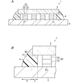
- FIG. 1A is a schematic cross-sectional view showing a semiconductor device according to one embodiment of the present disclosure.
- FIG. 1B is a schematic enlarged view showing an enlarged view of the dashed-dotted line portion of the semiconductor device shown in FIG. 1A.
- FIG. 2A is a plan view showing a first example of a semiconductor device according to an embodiment of the present disclosure, in which a side-fill material intervenes in the periphery of a mounted component.
- FIG. 2B is a plan view showing a second example in which a side-fill material is interposed in the peripheral portion of the mounted component in the semiconductor device according to the embodiment of the present disclosure;
- FIG. 2C is a plan view showing a third example in which the side-fill material is interposed in the peripheral portion of the mounted component in the semiconductor device according to the embodiment of the present disclosure;
- a side fill method As a side fill method.
- an epoxy resin composition such as that disclosed in Patent Document 1 (Japanese Unexamined Patent Publication No. 2013-102167) has been proposed.
- the inventors proceeded with research and development of a resin composition for encapsulation in order to solve the above-mentioned problems, and as a result of diligent studies, developed the side-fill resin composition of the present disclosure.
- the side-fill resin composition according to the present embodiment is a side filler interposed between the substrate 2 and the peripheral portion of the surface of the mounting component 3 surface-mounted on the substrate 2 facing the substrate 2. It is used to make the fill material 4 .
- the side-fill resin composition according to the present embodiment contains a cationic polymerizable component (A) and a photocationic polymerization initiator (B).
- the cationic polymerizable component (A) contains at least one resin selected from the oxetane compound (A1) and the alicyclic epoxy compound (A2).
- the ratio of the total amount of the oxetane compound (A1) and the alicyclic epoxy compound (A2) to the total amount of the cationic polymerizable component (A) in the side-fill resin composition is 70% by mass or more. Therefore, even if the side-filling resin composition of the present embodiment is interposed in a part of the gap between the substrate 2 and the mounting component 3 by the side-filling method to prepare the side-filling material 4, the side-filling resin composition High UV curability can be imparted to the resin composition, and excellent repairability can be imparted to the side-fill material 4 .
- the “side-fill material” is a material for reinforcing mounted parts such as semiconductor elements surface-mounted on a substrate.
- the side-fill material 4 is made of a cured side-fill resin composition. Further, the side-fill material 4 can also be said to be a reinforcing material interposed between the base material 2 and the periphery of the surface of the mounting component 3 facing the base material 2 .
- the peripheral portion of the surface of the mounted component 3 facing the substrate 2 may be the entire peripheral edge of the mounted component 3 in plan view, or may be at least a part of the entire peripheral edge.
- the side-fill resin composition of the present embodiment exhibits the above effects has not been clarified exactly, it is believed to be due to the following reasons. That is, by including the cationic polymerizable component (A) and the photocationic polymerization initiator (B) in the side-fill resin composition, UV curability can be imparted to the side-fill resin composition. Curing of both the compound (A1) and the alicyclic epoxy compound (A2) is likely to be accelerated by the acid generated from the photocationic polymerization initiator (B) upon UV irradiation.
- the ratio of the total amount of the oxetane resin (A1) and the alicyclic epoxy resin (A2) is 70% by mass or more with respect to the total amount of the cationic polymerizable component (A)
- high UV curability can be obtained. It is considered to be possible.
- the "UV curability" in the present disclosure can be measured by the same method as the evaluation shown in "2.3. UV curability" in the examples below, and can be confirmed based on the results obtained by the measurement.
- the side-fill resin composition of the present embodiment is interposed between the base material 2 and the mounting component 3 without being heated. It is possible to cure only by irradiating . Therefore, when the side-fill material 4 is produced from the side-fill resin composition, the adhesion strength between the base material 2 and the side-fill material 4 can be prevented from being excessively increased. Therefore, even when removing the side-fill material 4 formed on the base material 2 when a defect occurs in the semiconductor device 1 , it is easy to remove the residue of the side-fill material 4 from the base material 2 and the mounting components 3 .
- the side-filling material 4 on the base material 2 can be removed, for example, by heating to about the solder melting temperature (approximately 200° C.).
- solder melting temperature approximately 200° C.
- One of the reasons why the side-fill material 4 can be easily removed is considered to be due to the following action.
- an acid component by-produced from the cationic photopolymerization initiator (B) is incorporated into the cured product. can survive.
- the cured product is heated to a higher temperature, the acid component reacts with the cured product, and the cured product is thermally decomposed.
- the side-fill resin composition of the present embodiment can impart excellent repairability to the side-fill material.
- the term “repairability” as used in the present disclosure refers to the ease with which a cured product (including an underfill material and a sidefill material) produced from the resin composition in the semiconductor device 1 can be removed from the substrate 2. .
- the repairability of the cured product in the semiconductor device 1 can be confirmed by the method described in "2.4. Repairability" in the examples below.
- the side-fill resin composition of the present embodiment can be easily removed by heating the cured product produced from the side-fill resin composition. Even if a defect occurs in the semiconductor device 1, it can be easily repaired.
- the side-fill resin composition according to the present embodiment is provided between the substrate 2 of the semiconductor device 1 and the peripheral portion of the surface of the mounting component 3 mounted on the substrate 2 facing the substrate 2. , the connection between the base material 2 and the mounting component 3 can be reinforced.
- the preferable characteristics of the side-fill resin composition can be realized by appropriately adjusting the components of the composition described below.
- the side-fill resin composition of the present embodiment contains a cationic polymerizable component (A) and a photocationic polymerization initiator (B).
- the cationic polymerizable component (A) contains at least one of the oxetane compound (A1) and the alicyclic epoxy compound (A2).
- the ratio of the total amount of the oxetane compound (A1) and the alicyclic epoxy compound (A2) to the total amount of the cationically polymerizable component (A) is 70% by mass or more.
- the side-fill resin composition of the present embodiment has high UV curability.
- the side-fill material 4 interposed between the base material 2 and the periphery of the surface of the mounting component 3 facing the base material 2 is produced by irradiating light, the side-fill material 4 is The filling material 4 is less likely to have an uncured portion.
- the side-filling material 4 can have excellent heat resistance and repairability.
- a reinforcing material is produced from a thermosetting resin component in the presence of a curing agent by the side-fill method, it is possible to improve the repairability by adding an additive such as a softening agent. has been done. In this case, there is a problem that thermal properties such as heat resistance and thermal shock resistance of the semiconductor device 1 may deteriorate due to the influence of the softening agent.
- the semiconductor device 1 provided with the cured product of the side-fill resin composition can have excellent thermal shock resistance, and the flexibility-imparting agent
- the side-fill material 4 can have excellent repairability without adding additives such as For this reason, in the present embodiment, even if a defect occurs in the semiconductor device 1, the cured product can be easily removed by heating. It is easy to replace only the generated part.
- the side-fill resin composition of the present embodiment has UV curability as described above. For this reason, between the substrate 2 of the semiconductor device 1 and the mounting component 3 surface-mounted on the substrate 2, the peripheral portion of the surface of the mounting component 3 facing the substrate 2 is filled with the side-fill resin composition.
- the tact time for example, time for forming a cured product
- the side-fill material 4 is less likely to be affected by heat history due to heating. Therefore, the side-filling resin composition can reinforce the base material 2 and the peripheral edge portion of the mounted component 3 facing the base material 2 by making it difficult to detach the mounted component 3 in the semiconductor device 1, and the semiconductor device 1 can be made difficult to cause poor conduction.
- the side-fill resin composition of the present embodiment is more likely to suppress inclusion of air bubbles before and after curing when producing the side-fill material 4, compared to a composition containing a large amount of thermosetting resin components. For this reason, it is possible to prevent voids from forming in the cured product. As a result, even if the side-fill resin composition reinforces the peripheral portion of the surface of the mounting component 3 facing the base material 2, the semiconductor device 1 is defective. It is possible to make it less likely to occur.
- the side-fill resin composition is interposed between the substrate 2 in the semiconductor device 1 and the peripheral portion of the surface of the mounting component 3 surface-mounted on the substrate 2 facing the substrate 2, thereby By reinforcing the material 2 and the mounting component 3, the side-fill material 4 can be produced in a short time, and the side-fill material 4 is less likely to have a heat history. Therefore, the side-fill material 4 (reinforcing material) made from the side-fill resin composition is less likely to warp and void.
- the cationic polymerizable component (A) contains, for example, a photocationically polymerizable compound.
- the cationic polymerizable component (A) has a property of being cured by a polymerization reaction with an acid generated from the photocationic polymerization initiator (B).
- the cationic polymerizable component (A) preferably has the property of causing a ring-opening polymerization reaction with the photocationic polymerization initiator (B).
- the cationic polymerizable component (A) contains at least one of the oxetane compound (A1) and the alicyclic epoxy compound (A2) contained in the photocationically polymerizable compound.
- the total amount of the oxetane compound (A1) and the alicyclic epoxy compound (A2) is 70% by mass or more with respect to the total amount of the cationic polymerizable component (A).
- Heat cycle in the present disclosure refers to a temperature cycle in which heating and cooling are repeated between a low temperature range (eg ⁇ 40° C.) and a high temperature range (eg 125° C.).
- the cationically polymerizable component (A) in the present embodiment contains at least one of the oxetane compound (A1) and the alicyclic epoxy compound (A2), and the oxetane compound (A1) and the alicyclic Since the total amount with the formula epoxy compound (A2) is 70% by mass or more with respect to the total amount of the cationically polymerizable component (A), the side-fill resin composition is compared to the case where only the thermally polymerizable component is contained. can be easily made to have low viscosity. Therefore, in the side-fill resin composition, the viscosity of the side-fill resin composition is unlikely to increase even if the ratio of components such as the inorganic filler described later is increased. This makes it easy to adjust the coefficient of linear expansion of the cured product to be low, so that the thermal shock resistance of the semiconductor device 1 provided with the cured product produced from the side-fill resin composition can be improved. Therefore, the semiconductor device 1 can have high heat resistance reliability.
- the cationically polymerizable component (A) contains at least one of the oxetane compound (A1) and the alicyclic epoxy compound (A2), and the oxetane compound (A1 ) and the alicyclic epoxy compound (A2) is 70% by mass or more.
- the ratio of the total amount of the oxetane compound (A1) and the alicyclic epoxy compound (A2) to the total amount of the cationically polymerizable component (A) is more preferably 75% by mass or more, and even more preferably 80% by mass or more. , 85 mass % or more is particularly preferred.
- the upper limit of the ratio of the total amount of the oxetane compound (A1) and the alicyclic epoxy compound (A2) to the total amount of the cationically polymerizable component (A) is not particularly limited, it may be, for example, 100% by mass.
- the cationically polymerizable component (A) may contain only one of the oxetane compound (A1) and the alicyclic epoxy compound (A2), but the cationically polymerizable component (A) contains the oxetane compound ( It is more preferred to contain both A1) and the alicyclic epoxy compound (A2).
- the alicyclic epoxy compound (A2) is more susceptible to photoreaction at the initial stage of the reaction. It is highly resistant and facilitates the smooth progress of the reaction in the early stages of the curing reaction.
- the oxetane compound (A1) has a slower initial reaction rate than the alicyclic epoxy compound (A2), but the concentration of the cured product increases as the curing reaction of the alicyclic epoxy compound (A2) progresses. can gradually increase the reactivity of the oxetane compound (A1). Therefore, when the cationic polymerizable component (A) contains both the oxetane compound (A1) and the alicyclic epoxy compound (A2), the UV curability of the side-fill resin composition is likely to be further enhanced.
- the ratio of the oxetane compound (A1) and the alicyclic epoxy compound (A2) in the cationic polymerizable component (A) is within the range of 1:0 to 0:1. More preferably, the ratio of the oxetane compound (A1) to the alicyclic epoxy compound (A2) is within the range of 9:1 to 2:8, more preferably within the range of 9:1 to 3:7. is.
- the oxetane compound (A1) is, for example, a compound having at least one oxetane skeleton in one molecule.
- the oxetane compound (A1) includes, for example, 3-ethyl-3-hydroxymethyloxetane, 2-ethylhexyloxetane, 3-ethyl-3-(2-ethylhexyloxymethyl)oxetane, 3-ethyl-3
- At least one compound selected from the group consisting of -(cyclohexyloxy)methyloxetane and 3-ethyl-3-(phenoxymethyl)oxetane can be mentioned.
- the alicyclic epoxy compound (A2) has at least one epoxy group in one molecule, and two carbon atoms in the cyclic ether constituting the epoxy group are saturated or unsaturated without aromaticity. is a compound present on the carbocyclic ring of Specifically, the alicyclic epoxy compound (A2) includes, for example, 3′,4′-epoxycyclohexylmethyl 3,4-epoxycyclohexane carboxylate, 3,4-epoxycyclohexylmethyl (3′,4′-epoxy ) cyclohexane carboxylate, ⁇ -caprolactone-modified 3′,4′-epoxycyclohexylmethyl 3,4-epoxycyclohexane carboxylate, bis(3,4-epoxycyclohexyl) adipate, 1,2-epoxy-4-vinylcyclohexane, 1 ,4-cyclohexanedimethanol diglycidyl ether, epoxyethyl
- the cationically polymerizable component (A) is an oxetane compound ( A1) and a cationically polymerizable compound other than the alicyclic epoxy compound (A2) may be contained.
- the cationically polymerizable compound other than the oxetane compound (A1) and the alicyclic epoxy compound (A2) is, for example, selected from the group consisting of epoxy compounds (A3) other than the alicyclic epoxy compound (A2), and vinyl ether compounds. At least one may be included.
- the epoxy compound (A3) preferably has photocationic polymerizability. However, not limited to this, the epoxy compound (A3) may have thermosetting properties.
- the epoxy compound (A3) includes, for example, biphenyl-type epoxy resin, bisphenol A-type epoxy resin, bisphenol F-type epoxy resin, bisphenol S-type epoxy resin, naphthalene ring-containing epoxy resin, anthracene ring-containing epoxy resin, phenol At least one compound selected from the group consisting of novolak-type epoxy resins, cresol novolac-type epoxy resins, triphenylmethane-type epoxy resins, bromine-containing epoxy resins, and triglycidyl isocyanurate can be used.
- the epoxy resin may have a glycidyl group.
- the cationic polymerizable component (A) contains the epoxy compound (A3)
- the mass ratio of the epoxy compound (A3) to the total amount of the cationically polymerizable component (A) is more than 0% by mass and less than 30% by mass.
- a vinyl ether compound is, for example, a compound having at least one vinyl ether skeleton in one molecule.
- vinyl ether resins include ethylene glycol divinyl ether, diethylene glycol divinyl ether, triethylene glycol divinyl ether, polyethylene glycol divinyl ether, propylene glycol divinyl ether, butylene glycol divinyl ether, hexanediol divinyl ether, and bisphenol A alkylene oxide.
- At least one compound selected from the group consisting of divinyl ethers and bisphenol F alkylene oxide divinyl ethers can be mentioned.
- the mass ratio of the vinyl ether compound to the total amount of the cationically polymerizable component (A) is, for example, more than 0% by mass and less than 30% by mass.
- the cationically polymerizable component (A) is not limited to the above, and may be an appropriate monomer or oligomer having cationic polymerizability, or may contain a resin other than the above.
- the mass ratio of the cationic polymerizable component (A) to the total solid content of the side-fill resin composition is preferably 10% by mass or more and 60% by mass or less. In this case, higher UV curability can be imparted to the side-fill resin composition. Further, when the mass ratio of the cationic polymerizable component (A) to the total solid content of the side-fill resin composition is 10% by mass or more, the viscosity of the side-fill resin composition during molding can be better maintained. Cheap. Further, when the mass ratio is 60% by mass or less, the linear expansion coefficient of the cured product of the side-fill resin composition can be easily maintained low, and the thermal shock resistance of the semiconductor device 1 provided with this cured product can be easily improved.
- total solid content refers to the total amount of components other than volatilizable components such as solvents.
- the mass ratio of the cationically polymerizable component (A) to the total solid content of the side-fill resin composition is more preferably 10% by mass or more and 50% by mass or less, and even more preferably 10% by mass or more and 40% by mass or less. .
- the side-fill resin composition of the present embodiment contains a cationic photopolymerization initiator (B) contained in the cationic polymerization initiator.
- the photocationic polymerization initiator (B) can accelerate the curing reaction of the cationically polymerizable component (A) in the side-fill resin composition.
- the photocationic polymerization initiator (B) preferably has the function of, for example, a photoacid generator.
- a photoacid generator is a compound that has the function of polymerizing a polymerizable component by decomposing upon absorption of irradiated light and generating an acid.
- the photocationic polymerization initiator (B) contributes, for example, to curing the side-fill resin composition by irradiating it with light.
- the side-fill resin composition has photocurability, in the semiconductor device 1, the side-fill material 4 made of a cured product made from the side-fill resin composition can be removed more easily.
- the photocationic polymerization initiator (B) includes a polymerization initiator containing an appropriate onium cation as a cationic species and an appropriate anionic species.
- Onium cations include, for example, sulfonium cations and iodonium cations.
- anionic species include PF 6 - , B(C 6 F 5 ) 4 - , SbF 6 - , CF 3 SO 3 - , CF 3 (CF 2 ) 3 SO 3 - , p-CH 3 (CH 2 ) 10
- anion selected from the group consisting of C 6 H 4 SO 3 ⁇ , dinonylnaphthalenesulfonate anions, and p-toluenesulfonate anions can be used.
- the photocationic polymerization initiator (B) is, for example, triarylsulfonium.(Rf) n PF 6-n salt, triarylsulfonium.PF 6 salt, triarylsulfonium.SbF 6 salt, triarylsulfonium.B(C 6 F 5 ) tetrasalt, bis[ 4 -n-alkyl(C10-C13)phenyl]iodonium hexafluorophosphate, bis[4-n-alkyl(C10-C13)phenyl]iodonium hexafluoroantimonate, bis[4-n -Alkyl(C10-C13)phenyl]iodonium tetrakis(pentafluorophenyl)borate and bis(4-tert-butylphenyl)iodonium hexafluorophosphate.
- the photocationic polymerization initiator (B) preferably generates an acid by irradiation with light having a wavelength of, for example, 200 nm or more and 400 nm or less.
- Examples of specific commercial products of the photocationic polymerization initiator (B) include sulfonium salts (triarylsulfonium salt types CPI-100P, CPI-101A, CPI-200K, CPI-210S, CPI -310B, CPI-410S), iodonium salts (IK-1, etc.), and WPI series of iodonium salts manufactured by Fujifilm Wako Pure Chemical Industries, Ltd. (WPI-113, WPI-116, WPI-124, WPI-170, etc.) etc. can be mentioned.
- the ratio of the photocationic polymerization initiator (B) to 100 parts by mass of the cationic polymerizable component (A) is preferably 0.1 parts by mass or more and 10 parts by mass or less. In this case, it is easy to further improve the repairability of the cured product produced from the side-fill resin composition.
- the ratio of the photocationic polymerization initiator (B) to 100 parts by mass of the cationic polymerizable component (A) is more preferably 0.3 parts by mass or more and 8 parts by mass or less, and more preferably 0.5 parts by mass or more and 5 parts by mass or less. is even more preferable.
- the resin composition for side-fill material preferably further contains an inorganic filler (C).
- C the coefficient of thermal expansion of a cured product produced from the side-fill resin composition
- the side-fill material 4 is less likely to warp, thereby making it more difficult for the semiconductor device 1 to be defective due to heat generation or the like.
- the mass ratio of the inorganic filler (C) to the total solid content of the side-fill resin composition is preferably 10% by mass or more and 90% by mass or less. In this case, it is easier to lower the CTE of the cured product produced from the side-fill resin composition. More preferably, the mass ratio of the inorganic filler (C) to the total solid content of the side-fill resin composition is 30% by mass or more and 90% by mass or less. When the mass ratio of the inorganic filler (C) to the total solid content of the side-fill resin composition is 30% by mass or more, the CTE of the cured product of the side-fill resin composition can be further lowered, and the semiconductor device 1 The heat resistance reliability of can be easily improved.
- the side-fill resin composition can be adjusted to be excellently liquid. More preferably, the mass ratio of the inorganic filler (C) to the total solid content of the side-fill resin composition is 50% by mass or more and 90% by mass or less.
- the inorganic filler (C) includes, for example, at least one material selected from the group consisting of silica, alumina, clay, mica, talc, aluminum hydroxide, magnesium hydroxide, calcium carbonate, and glass.
- Silica can be, for example, fused silica, crystalline silica, fumed silica, and the like.
- the silica may be surface-treated.
- the silica is surface-treated, the cationically polymerizable component (A) and silica in the side-fill resin composition can be made more compatible, and the dispersibility of the side-fill resin composition can be improved.
- the surface treatment of silica can be realized, for example, by treating silica with a silane coupling agent.
- silane coupling agents include compounds having at least one functional group selected from the group consisting of epoxy groups, amino groups, (meth)acryloyl groups, and phenyl groups.
- the average particle size of the inorganic filler (C) is preferably, for example, 2.5 ⁇ m or more and 200 ⁇ m or less.
- the side-fill resin composition is interposed between the base material 2 and the periphery of the surface of the mounting component 3 facing the base material 2. In this case, better fluidity of the side-fill resin composition can be maintained.
- the “average particle diameter” in the present disclosure is the volume-based median diameter D50.
- the median diameter D50 is calculated from the particle size distribution measured by a laser diffraction/scattering method. The particle size distribution can be measured, for example, with a laser diffraction particle size distribution analyzer.
- the side-fill resin composition can contain components other than the components described above as long as the effects of the present disclosure are not impaired.
- the side-fill resin composition may contain resin components other than the resins described above.
- the side-fill resin composition may contain, for example, a radically polymerizable compound.
- the encapsulating resin composition can contain appropriate additives.
- additives include curing agents, stabilizers, photosensitizers, fluxes, viscosity modifiers, thixotropic agents, surface modifiers, silane coupling agents, antifoaming agents, leveling agents, and low stress agents. , and pigments.
- the side-fill resin composition may contain a thixotropic agent. In this case, in supplying the side-fill resin composition to the peripheral portion of the surface of the mounting component 3 facing the substrate 2 between the substrate 2 and the mounting component 3 of the semiconductor device 1, the side-filling resin It is easy to ensure better fluidity and thixotropy of the composition. As a result, the side-fill resin composition can have higher moldability. 4 can be given excellent strength.
- the side-fill resin composition may contain a stabilizer.
- a stabilizer such as an appropriate antioxidant can be employed.
- the side-fill resin composition may contain a softening agent.
- a softening agent when a defect occurs in the semiconductor device 1 and repair is performed, the repairability can be further improved.
- the side-fill resin composition of the present embodiment can achieve high repairability even if it does not contain a softening agent.
- the side-fill resin composition may contain a photosensitizer. In this case, the curing reaction of the side-fill resin composition can be accelerated. Therefore, the tact time can be shortened in producing a cured product from the side-fill resin composition.
- the side-fill resin composition preferably does not contain an organic solvent or has an organic solvent content of 0.5% by mass or less. In this case, the viscosity when molding the side-fill resin composition can be easily maintained.
- the side-fill resin composition can be obtained, for example, by blending the above components, adding appropriate additives as necessary, and mixing. Specifically, the side-fill resin composition can be prepared, for example, by the following method.
- a mixture is obtained by blending the components that can be contained in the side-fill resin composition described above either simultaneously or sequentially. This mixture is stirred and mixed while heat treatment or cooling treatment is performed as necessary.
- additives are added to this mixture, and while performing heat treatment or cooling treatment as necessary, they are stirred again and mixed until they are uniformly dispersed. Thereby, the side-fill resin composition can be obtained.
- a disper for example, a disper, a planetary mixer, a ball mill, a three-roll mill, a bead mill, and the like can be used in combination as necessary.
- the viscosity of the side-fill resin composition at 25°C is preferably 10 Pa ⁇ s or more and 2000 Pa ⁇ s or less. In this case, it is easy to ensure the moldability of the side-fill resin composition. In this case, it is also possible to achieve good filling between the substrate 2 and the periphery of the surface of the mounting component 3 such as a semiconductor chip that faces the substrate 2 .
- the viscosity of the side-fill resin composition at 25° C. can be measured with a Brookfield viscometer under conditions of rotor No. 7, number of rotations of 1 to 50 rpm, and measurement time of 60 to 180 seconds.
- the conditions for measuring the viscosity are appropriately adjusted depending on the composition of the resin composition, etc., but the rotation speed is set to the maximum measurable rotation speed for the resin composition, and the measurement time is It can be measured by setting the time for the rotor to rotate 3 times or more with respect to the composition.
- a specific measuring method will be described in detail in Examples below.
- the viscosity of the side-fill resin composition at 25° C. is more preferably 1000 Pa ⁇ s or less, more preferably 700 Pa ⁇ s or less, and particularly preferably 400 Pa ⁇ s or less.
- the viscosity of the side-fill resin composition at 25° C. is more preferably 50 Pa ⁇ s or more, and even more preferably 100 Pa ⁇ s or more.
- the side-fill resin composition of the present embodiment has photocurability. Therefore, the side-fill resin composition can be cured by irradiating it with light.
- Conditions for irradiating light such as light irradiation wavelength, light irradiation intensity (light amount), light irradiation time, heating temperature, and heating time, are the components that can be contained in the side-fill resin composition, For example, it may be appropriately adjusted according to the type of the cationic polymerizable component (A), the type of the cationic photopolymerization initiator (B), and the like.
- an appropriate light source can be adopted, such as chemical lamps, low-pressure mercury lamps, medium-pressure mercury lamps, high-pressure mercury lamps, ultra-high-pressure mercury lamps, xenon lamps, metal halide lamps, At least one light source selected from the group consisting of LED, YAG, g-line (436 nm), h-line (405 nm), i-line (365 nm), and combinations of two or more of g-line, h-line and i-line can be The light source is not limited to these, and any light source may be used as long as it can irradiate ultraviolet rays capable of curing the side-fill resin composition.
- the side-fill resin composition can be heated by an appropriate heating device.
- the glass transition temperature (Tg) of the cured product of the side-fill resin composition is preferably 130°C or higher. If the glass transition temperature is 130° C. or higher, the cured product of the side-fill resin composition can have heat resistance.
- the glass transition temperature can be measured, for example, by TMA (Thermomechanical Analysis).
- TMA Thermomechanical Analysis
- the cured product of the side-fill resin composition can be made less likely to soften even in a high temperature range (for example, around 125° C.) in a heat cycle test. Therefore, the side-fill resin composition can ensure high heat resistance reliability in the semiconductor device 1 .
- the semiconductor device 1 when the mounted parts on the substrate are reinforced with a side-fill material made of a cured product of a conventional resin composition, the semiconductor device 1 is exposed to a severe thermal environment (for example, ⁇ 40° C. or lower, and 125° C. or higher), poor conduction between the substrate and the mounted components may occur.
- a severe thermal environment for example, ⁇ 40° C. or lower, and 125° C. or higher
- the cured product of the side-filling resin composition is , can impart high thermal shock resistance to the semiconductor device 1 . For this reason, in the present embodiment, it is possible to make the semiconductor device 1 less susceptible to defective conduction.
- the linear expansion coefficient (CTE) of the cured product of the side-fill resin composition below the glass transition temperature Tg is less than 40 ppm/°C.
- the side-filling material 4 made of the cured side-filling resin composition is less likely to warp. It is possible to make it difficult for peeling to occur. Therefore, cracks are less likely to occur in the cured product of the encapsulating resin composition. Therefore, the side-fill material 4 made from the side-fill resin composition can further improve the heat resistance reliability of the semiconductor device 1 .
- the CTE of the cured product of the side-fill resin composition at Tg or lower is more preferably 35 ppm/°C or lower, and even more preferably 30 ppm/°C or lower.
- the CTE of the cured product of the side-fill resin composition below Tg can be obtained by calculating the slope of the tangential line based on the dimensional change between any two temperatures below Tg.
- the side-fill resin composition of the present embodiment can be suitably used as a side-fill material as already described.
- the side-fill resin composition can be particularly suitably used as a post-supply type side-fill material in flip-chip mounting.
- the side-fill resin composition according to the present embodiment can be suitably used for producing the side-fill material 4 that reinforces the base material 2 and the mounting component 3 in the semiconductor device 1 .
- the side-filling resin composition in reinforcing the base material 2 and the mounting component 3, the side-filling resin is Reinforcement can be achieved simply by supplying the composition, and the supply amount of the resin composition can be reduced compared to an underfill material that fills the entire gap between the base material 2 and the mounting component 3 . In this case, it is possible to make it difficult for the reinforced mounting component 3 to detach, and to make it difficult for the semiconductor device 1 to have poor conduction.
- the side-fill material 4 for supporting the base material 2 and the mounted parts 3 is provided. (Specifically, only the side-fill material 4 intervening in the peripheral portion of the mounting component 3) needs to be peeled off, so repair can be performed without discarding normal members. Also, the side-fill material 4 of the present embodiment can be easily removed without being heated to an excessively high temperature. Therefore, in the semiconductor device 1, the side-fill material 4 produced from the side-fill resin composition of the present embodiment is excellent in repairability. Furthermore, in repairing the semiconductor device 1, as described above, it is possible to reduce the disposal of parts other than the defective part, which contributes to cost reduction when a defect occurs, compared to the underfill material.
- the semiconductor device 1 of this embodiment includes a base material 2 , a mounting component 3 and a side-fill material 4 .
- Mounted component 3 is surface-mounted on substrate 2 .
- the side-fill material 4 is interposed between the periphery of the surface of the mounting component 3 facing the base material 2 .
- the side-fill material 4 is made of a cured product of the side-fill resin composition described above.
- FIG. 1A shows an example of the semiconductor device 1 of this embodiment.
- a semiconductor device 1 includes a substrate 2 that supports a mounted component 3 such as a semiconductor chip, a mounted component 3 that is surface-mounted face-down on the substrate 2, and a substrate between the substrate 2 and the mounted component 3.
- a side-fill material 4 interposed between the material 2 and the peripheral edge portion of the surface of the mounting component 3 facing the base material 2 is provided.
- the side-fill material 4 can support the base material 2 and the mounted component 3 between the base material 2 and the periphery of the mounted component 3 . That is, in the semiconductor device 1 shown in FIG. fills only the space between As a result, the side-fill material 4 reinforces the mounting component 3 surface-mounted on the base material 2 at the peripheral end portion of the mounting component 3 .
- the side-filling material 4 is formed between the base material 2 and the mounting component 3 by applying the side-filling resin composition to the base material 2 and part or all of the periphery of the surface of the mounting component 3 facing the base material 2. It is formed by supplying to and photocuring.
- the side-fill resin composition is applied to the inner side of the peripheral portion of the surface of the mounting component 3 facing the substrate 2 in plan view (that is, the gap between the substrate 2 and the mounting component 3 in the peripheral portion of the mounting component 3). However, as shown in FIG.
- the permeation distance b is the side-fill resin composition from the position corresponding to the outer peripheral edge of the mounted component 3 to the mounted component It is preferably equal to or shorter than the distance a to the outer position of the surface where the substrate 3 and the substrate 2 face each other (that is, b ⁇ a).
- the infiltration distance is the distance between the surface of the mounted component 3 facing the substrate 2 and the inner side of the surface where the mounted component 3 and the substrate 2 face each other from a position corresponding to the outer peripheral edge of the mounted component 3 in a plan view. It is the length that the side-fill resin composition has penetrated into the position.
- the semiconductor device 1 and the manufacturing method thereof according to this embodiment will be specifically described.
- a semiconductor device 1 includes a substrate 2 having conductor wiring 21, and a mounting component 3 such as a semiconductor chip, which is provided with bump electrodes 33 and mounted on the substrate 2 by bonding the bump electrodes 33 to the conductor wiring 21. , and a sidefill material 4 (see FIG. 1A).
- the side-fill material 4 is a cured product of the side-fill resin composition described above.
- the base material 2 is, for example, a mother board, a package board or an interposer board.
- the base material 2 includes an insulating substrate made of glass epoxy, polyimide, polyester, ceramic, or the like, and conductor wiring 21 made of a conductor such as copper formed on the surface thereof.
- the conductor wiring 21 includes, for example, electrode pads.
- the side-fill resin composition of the present embodiment can be suitably used for printed wiring boards. Therefore, the substrate 2 may be a substrate of an appropriate printed wiring board, and examples of substrates of the printed wiring board include organic resin substrates such as FR-4, ceramic substrates, metal base substrates, glass substrates, and the like. be done.
- the mounted component 3 is, for example, a semiconductor chip.
- the semiconductor chip is a flip-chip type chip such as BGA (Ball Grid Array), LGA (Land Grid Array) or CSP (Chip Size Package).
- the semiconductor chip may be a PoP (package on package) type chip.
- the mounting component 3 may have a plurality of bump electrodes 33 .
- the bump electrodes 33 are provided with solder.
- the bump electrode 33 includes a pillar 31 and a solder bump 32 provided at the tip of the pillar 31, as shown in FIG.
- the solder bumps 32 are made of solder, so the bump electrodes 33 comprise solder.
- the pillar 31 is made of copper, for example.
- the melting point of the solder provided in the bump electrode 33 is not particularly limited, but can be melted below the mounting temperature (for example, 220 to 260° C.) when mounting the mounted component 3 such as a semiconductor chip. Any temperature is acceptable.
- the composition of the solder is not particularly limited, and may be an appropriate composition. For example, Sn--Ag-based solder and Sn--Ag--Cu-based solder can be used.
- the structure of the bump electrode 33 including solder is not limited to the above.
- the bump electrode 33 may include only spherical solder bumps 32 (solder balls). That is, the bump electrode 33 may not have pillars.
- the method for manufacturing the semiconductor device 1 of this embodiment includes a coating process and a curing process.
- the application step includes applying the side-fill resin composition to the periphery of the surface of the mounting component 3 facing the substrate 2 .
- the curing step includes a step of curing the side-fill resin composition applied in the coating step.
- the volume of the side-fill material 4 interposed between the base material 2 and the mounted component 3 at the peripheral edge portion of the surface of the mounted component 3 facing the base material 2 and the mounted component 3 is above the base material 2. It is preferable to apply so that the volume is smaller than the volume of the side-fill material 4 intervening only.
- the tact time for manufacturing the semiconductor device 1 can be shortened while improving the reinforcing strength of the cured product of the side-fill resin composition between the substrate 2 and the mounting component 3 in the semiconductor device 1 .
- the curing step includes irradiating the side-fill resin composition with light.
- the side-fill resin composition is applied to the periphery of the mounting component 3, and then the side-fill resin composition is irradiated with light to cure the side-fill.
- Curing the resin composition for Irradiation of light in the curing step is not particularly limited, but can be realized by an appropriate light source. That is, the conditions for light irradiation and the light source may be the same as those already described. In the above description, curing is performed by irradiating the side-fill resin composition with light. You may heat as an after-cure.
- the side-fill material 4 fills the gap between the base material 2 and the mounted component 3 , and fills the gap between the base material 2 and the mounted component 3 at the periphery of the surface of the mounted component 3 facing the base material 2 . It fills only the gap between the department. Specifically, the side-fill material 4 fills the outer side of the peripheral edge portion and a part of the inner side of the peripheral edge portion of the surface of the mounting component 3 facing the base material 2 .
- the side-fill material filling the outer side of the peripheral portion is sometimes called the first side-filling material 41
- the side-filling material partially filling the inner side of the peripheral portion is sometimes called the second side-filling material 42 .
- 1B schematically shows the first side-fill material 41 and the second side-fill material 42, and the shapes and exact positions of the first side-fill material 41 and the second side-fill material 42. does not indicate
- the side-filling material 4 intervenes the mounting component 3 surface-mounted on the base material 2 in the peripheral edge portion of the surface of the mounting component 3 facing the base material 2 , so that the base material 2 and the mounting component 3 is reinforced.
- the side-fill material 4 in the semiconductor device 1 is interposed only on the base material 2 at the periphery of the surfaces of the base material 2 and the mounting component 3 facing the base material 2 (that is, the first side-fill material 41 ) is preferably larger than the volume of the side-fill material 4 (that is, the second side-fill material 42 ) interposed in the gap between the base material 2 and the mounted component 3 .
- the side-fill resin composition has excellent UV curability. It can be produced by irradiating light from
- a method for manufacturing the semiconductor device 1 will be described with an example. Note that the method for manufacturing the semiconductor device 1 is not limited to the method described below.
- the side-fill resin composition described above is interposed in part or all of the peripheral portion of the surface facing the substrate 2 of the mounting component 3 surface-mounted on the substrate 2. , the side-fill material 4 is produced, and the semiconductor device 1 can be produced.
- the substrate 2 having the conductor wiring 21 and the mounting component 3 having the bump electrode 33 are prepared.
- the conductor wiring 21 and the bump electrode 33 may be electrically connected by heating, for example.
- the side-fill resin composition is supplied to the peripheral portion of the surface facing the substrate 2 in the mounted component 3 surface-mounted on the substrate 2, and then the supplied side
- the side-fill resin composition is cured by irradiating the fill resin composition with light.
- the side-fill material 4 is produced on the base material 2 and the peripheral portion of the mounting component 3 facing the base material 2 .
- the curing conditions for the side-fill resin composition are as described above.
- the side-fill resin composition can be arranged so as to be interposed between the base material 2 and part or all of the peripheral edge of the surface of the mounting component 3 facing the base material 2. , the side-fill resin composition may be placed at any position on the mounting component 3 and the substrate 2 at any time.
- FIGS. 2A to 2C A specific example of the position of the side-fill material 4 in the semiconductor device 1 will be described with reference to FIGS. 2A to 2C. However, the position of the side-fill material 4 in the semiconductor device 1 is not limited to these.
- FIGS. 2A to 2C show, in the semiconductor device 1, a side fill between the substrate 2 and the peripheral portion of the surface of the mounting component 3 surface-mounted on the substrate 2 facing the substrate 2 in a plan view.
- the side-fill material 4 is produced by supplying and curing the resin composition. That is, FIGS. 2A to 2C show examples (first to third examples) in which the substrate 2 and the periphery of the mounting component 3 are reinforced with the side-fill material 4.
- the side-fill resin composition of the present embodiment can reinforce the base material 2 and the mounting component 3 in the semiconductor device 1 by simply supplying the peripheral portion of the mounting component 3 .
- the side-fill material 4 made from the side-fill resin composition supports the periphery of the mounting component 3 in the semiconductor device 1 . That is, in the present embodiment, the side-fill material 4 does not intervene in the entire gap between the base material 2 and the mounting component 3, and only the peripheral portion is supported by the side-fill material 4. 2 and the mounting component 3 are less likely to warp.
- a side-fill material 4 made of a cured side-fill resin composition is formed on the entire peripheral edge of the surface of the mounting component 3 facing the base material 2 .
- the strength to reinforce the substrate 2 and the mounted component 3 in the semiconductor device 1 can be increased, and the substrate 2 and the mounted component 3 are less likely to warp.
- the substrate 2 and a plurality of corners (more specifically, a substantially rectangular mounted component in a plan view) of the periphery of the surface of the mounted component 3 facing the 3) are formed with a side-fill material 4 made of a cured product of a side-fill resin composition.
- a side-fill material 4 made of a cured product of a side-fill resin composition.
- a side-filling material made of a cured side-filling resin composition is applied to the corners of the peripheral portion of the surface facing the base material 2 of the mounting component 3 and to the two opposing sides. formed.
- the strength that reinforces the base material 2 and the mounting component 3 in the semiconductor device 1 can be maintained, and the base material 2 and the mounting component 3 are less likely to warp.
- the side-fill material produced from the side-fill resin composition of the present embodiment when a defect occurs, it is easy to replace only the portion where the defect occurs.
- the method for removing the side-filling material of the present embodiment removes the side-filling material 4 from between the peripheral portion of the mounting component 3 and the base material 2 while the side-filling material 4 in the semiconductor device 1 is heated to 200° C. or higher. do.
- the side-fill material 4 can be removed by heating to the melting temperature (approximately 200° C.) or higher of the solder material. Therefore, according to the method of removing the side-fill material 4 of this embodiment, the semiconductor device 1 can be easily repaired.
- Oxetane compound 2 Photo-cationically polymerizable compound (product name: ETERNACOLL OXBP, manufactured by Ube Industries, Ltd.).
- - Alicyclic epoxy compound 1 photo cationic polymerizable compound (product name of Daicel Co., Ltd. Celoxide 2021).
- - Alicyclic epoxy compound 2 photo cationic polymerizable compound (product name of Daicel Corporation, Celoxide 8000).
- - Alicyclic epoxy compound 3 photo cationic polymerizable compound (product name of Daicel Co., Ltd. Celoxide 2081).
- Other epoxy compound 1 DIC Corporation product name Epiclon 840A.
- Cationic polymerization initiator 1 San-Apro Co., Ltd.
- Product name CPI-200K Photocationic polymerization initiator.
- Cationic polymerization initiator 2 BASF product name: IRGACURE 290 (Photocationic polymerization initiator, triarylsulfonium tetrakis-(pentafluorophenyl)borate.) Non-antimony photoacid generator.
- Heat curing agent ⁇ Heat curing agent 1: acid anhydride curing agent (DIC Corporation product name B650) • Thermal curing agent 2: imidazole-based curing agent (2MAOK manufactured by Shikoku Kasei Kogyo Co., Ltd.). (Additives, etc.) ⁇ Inorganic filler: MRC Unitech Co., Ltd. product name QS-6 (30 ⁇ m cut). • Thixotropic agent: Nippon Aerosil Co., Ltd. product name RY200. ⁇ Softening agent: Product name LBR-302 manufactured by Kuraray Co., Ltd.
- the side-fill resin composition prepared in is applied to the substrate, and an LED UV irradiator (manufactured by Panasonic Industrial Devices SUNX Co., Ltd., model number Aicure UD40) is used to apply the side-fill resin composition to the upper surface of the substrate (side to which the side-fill resin composition is applied).
- the substrate and the side-fill resin composition after photocuring applied on the substrate were placed in a heating furnace and heated at 100° C. for 30 minutes to cure.
- Comparative Examples 3 to 5 the above 1.
- the side-fill resin composition prepared in 1. is applied to a substrate, and the substrate and the side-fill resin composition coated on the substrate are placed in a heating furnace and heated at a heating temperature of 150 ° C. for a heating time of 30 minutes. By doing so, it was hardened.
- a cured product of the side-fill resin composition of each of the obtained examples and comparative examples (hereinafter sometimes referred to as each example) was cut into a width of 5 mm, a length of 50 mm, and a thickness of 0.2 mm. , to prepare a test piece.
- the test piece was heated by the TMA method using a thermal analysis device (manufactured by Hitachi High-Tech Science Co., Ltd. model number TMA7100) at a temperature increase rate of 5 ° C./min and a measurement temperature of 30 to 260 ° C. , the coefficient of linear expansion ⁇ 1 below Tg in the temperature range of 50° C. to 70° C. was calculated.
- Tables 1 to 3 show the linear expansion coefficient ⁇ 1 (ppm/°C) of the cured product thus obtained.
- Viscosity 1 above The side-fill resin composition prepared in 1. is placed in a cylindrical container, and the rotor No. 7. Viscosity was measured at a measurement temperature of 25°C.
- the rotation speed of the viscometer was set to the highest measurable rotation speed in the range of 1 to 50 rpm, and the measurement time was within the range of 60 seconds to 180 seconds, the time during which the rotor rotated three times or more.
- the rotation speed was 10 rpm and the measurement time was 60 seconds.
- Comparative Example 5 the rotation speed was 5 rpm and the measurement time was 60 seconds.
- Example 14 the rotation speed was 2.5 rpm and the measurement time was 90 seconds.
- Example 17 the rotation speed was 1 rpm and the measurement time was 180 seconds. The results obtained from these are shown in Tables 1-3.
- Curing rate (R [%]) [1-(x2) / ((x1) + (x2))] x 100
- Temperature cycle (TC) resistance Mounting an IC chip for mounting (Waltz WLP TEG ⁇ 0.3 mm pitch BGA>, 6 mm) on an FR-4 circuit board (Waltz WALTS KIT WLP300P) with daisy chain electrodes created TEG (Test Element Group).
- TEG Temperature cycle
- the side-fill resin composition prepared in 1. was applied so as to have a width of 0.8 mm and a height of 0.4 mm so as to have a plan view shape (L-shape at four corners) shown in FIG. 2B.
- the length of the contact portion between the side-fill resin composition and the IC chip was set to 2.5 mm.
- the coated side-fill resin composition was irradiated with light and then heated in a heating furnace to prepare a test piece having a cured product of the side-fill resin composition on the TEG.
- the curing conditions are the same as the light irradiation conditions or heating conditions in 2.1 above.
- a heat cycle test was performed on the prepared test piece using a thermal shock tester (manufactured by Espec Co., Ltd., model number TSE-12-A).
- a thermal shock tester manufactured by Espec Co., Ltd., model number TSE-12-A.
- the operation was confirmed by measuring the resistance value of the test piece every 100 cycles.
- the change in the resistance value of the test piece increased by 5% or more from the start of the test, it was determined to be malfunctioning, and evaluated according to the following criteria. The results are shown in Tables 1-3.
- B Malfunction occurs between 500 cycles and 2000 cycles.
- C Malfunction occurs during less than 500 cycles.
- the resin composition was applied onto the glass plate from a syringe filled with the resin composition by a dispensing robot manufactured by Musashi Engineering Co., Ltd. (model number SHOTMASTER300 ⁇ X).
- the coating conditions were such that the distance between the glass plate and the tip of the needle was 0.5 mm, the moving speed was 3 mm/s, and the coating was applied in a straight line with a length of 10 cm.
- the state of the resin after application was visually observed and evaluated according to the following criteria.
- B Application was possible, but there was a part that was interrupted on the way.
- C It was impossible to eject from the needle.
- the rotation speed was 10 rpm and the measurement time was 60 seconds.
- the rotation speed was 5 rpm and the measurement time was 60 seconds.
- the rotation speed was 2.5 rpm and the measurement time was 90 seconds.
- the rotation speed was 1 rpm and the measurement time was 180 seconds. This was taken as the viscosity immediately after producing the side-fill resin composition.
- the side-fill resin compositions were treated under the same conditions. The viscosity of the resin composition for was measured.
- Pot life was evaluated according to the following criteria based on the obtained viscosity immediately after preparation and viscosity after each time.
Landscapes
- Chemical & Material Sciences (AREA)
- Health & Medical Sciences (AREA)
- Chemical Kinetics & Catalysis (AREA)
- Medicinal Chemistry (AREA)
- Polymers & Plastics (AREA)
- Organic Chemistry (AREA)
- Epoxy Resins (AREA)
Priority Applications (3)
| Application Number | Priority Date | Filing Date | Title |
|---|---|---|---|
| JP2023512952A JPWO2022215577A1 (https=) | 2021-04-05 | 2022-03-28 | |
| CN202280023638.XA CN117099198A (zh) | 2021-04-05 | 2022-03-28 | 侧填充用树脂组合物、半导体装置、侧填充构件的除去方法和半导体装置的制造方法 |
| US18/552,867 US20240186203A1 (en) | 2021-04-05 | 2022-03-28 | Side-filling resin composition, semiconductor device, method for removing side-filling member, and method for fabricating the semiconductor device |
Applications Claiming Priority (2)
| Application Number | Priority Date | Filing Date | Title |
|---|---|---|---|
| JP2021-064319 | 2021-04-05 | ||
| JP2021064319 | 2021-04-05 |
Publications (1)
| Publication Number | Publication Date |
|---|---|
| WO2022215577A1 true WO2022215577A1 (ja) | 2022-10-13 |
Family
ID=83545460
Family Applications (1)
| Application Number | Title | Priority Date | Filing Date |
|---|---|---|---|
| PCT/JP2022/014998 Ceased WO2022215577A1 (ja) | 2021-04-05 | 2022-03-28 | サイドフィル用樹脂組成物、半導体装置、サイドフィル材の除去方法、及び半導体装置の製造方法 |
Country Status (4)
| Country | Link |
|---|---|
| US (1) | US20240186203A1 (https=) |
| JP (1) | JPWO2022215577A1 (https=) |
| CN (1) | CN117099198A (https=) |
| WO (1) | WO2022215577A1 (https=) |
Citations (4)
| Publication number | Priority date | Publication date | Assignee | Title |
|---|---|---|---|---|
| JP2004273554A (ja) * | 2003-03-05 | 2004-09-30 | Mitsubishi Electric Corp | 中空構造を有する半導体装置 |
| JP2015153765A (ja) * | 2014-02-10 | 2015-08-24 | パナソニックIpマネジメント株式会社 | 回路装置の製造方法、半導体部品の実装構造および回路装置 |
| WO2019098053A1 (ja) * | 2017-11-14 | 2019-05-23 | 株式会社弘輝 | 補強用樹脂組成物及び電子部品装置 |
| WO2021157472A1 (ja) * | 2020-02-04 | 2021-08-12 | パナソニックIpマネジメント株式会社 | サイドフィル用樹脂組成物、半導体装置、及びサイドフィル材の除去方法 |
Family Cites Families (4)
| Publication number | Priority date | Publication date | Assignee | Title |
|---|---|---|---|---|
| US6589802B1 (en) * | 1999-12-24 | 2003-07-08 | Hitachi, Ltd. | Packaging structure and method of packaging electronic parts |
| JP2005033053A (ja) * | 2003-07-08 | 2005-02-03 | Lintec Corp | 半導体装置の製造方法及び半導体装置 |
| US20060223978A1 (en) * | 2005-04-04 | 2006-10-05 | Shengqian Kong | Radiation- or thermally-curable oxetane barrier sealants |
| JP5973431B2 (ja) * | 2011-05-31 | 2016-08-23 | デンカ株式会社 | エネルギー線硬化性樹脂組成物 |
-
2022
- 2022-03-28 CN CN202280023638.XA patent/CN117099198A/zh active Pending
- 2022-03-28 WO PCT/JP2022/014998 patent/WO2022215577A1/ja not_active Ceased
- 2022-03-28 US US18/552,867 patent/US20240186203A1/en active Pending
- 2022-03-28 JP JP2023512952A patent/JPWO2022215577A1/ja active Pending
Patent Citations (4)
| Publication number | Priority date | Publication date | Assignee | Title |
|---|---|---|---|---|
| JP2004273554A (ja) * | 2003-03-05 | 2004-09-30 | Mitsubishi Electric Corp | 中空構造を有する半導体装置 |
| JP2015153765A (ja) * | 2014-02-10 | 2015-08-24 | パナソニックIpマネジメント株式会社 | 回路装置の製造方法、半導体部品の実装構造および回路装置 |
| WO2019098053A1 (ja) * | 2017-11-14 | 2019-05-23 | 株式会社弘輝 | 補強用樹脂組成物及び電子部品装置 |
| WO2021157472A1 (ja) * | 2020-02-04 | 2021-08-12 | パナソニックIpマネジメント株式会社 | サイドフィル用樹脂組成物、半導体装置、及びサイドフィル材の除去方法 |
Also Published As
| Publication number | Publication date |
|---|---|
| CN117099198A (zh) | 2023-11-21 |
| US20240186203A1 (en) | 2024-06-06 |
| JPWO2022215577A1 (https=) | 2022-10-13 |
Similar Documents
| Publication | Publication Date | Title |
|---|---|---|
| KR100556981B1 (ko) | 전자부품 | |
| JP6155261B2 (ja) | 半導体パッケージ樹脂組成物及びその使用方法 | |
| JP3971995B2 (ja) | 電子部品装置 | |
| JP2011071108A (ja) | 異方性導電材料及び接続構造体 | |
| JP7591720B2 (ja) | サイドフィル用樹脂組成物、半導体装置、及びサイドフィル材の除去方法 | |
| JP2010174077A (ja) | 電子部品用接着剤 | |
| JP3644340B2 (ja) | エポキシ樹脂組成物 | |
| WO2022215577A1 (ja) | サイドフィル用樹脂組成物、半導体装置、サイドフィル材の除去方法、及び半導体装置の製造方法 | |
| JP2004204047A (ja) | 液状エポキシ樹脂組成物 | |
| JP4836325B2 (ja) | 封止樹脂用組成物 | |
| JP2012012431A (ja) | 液状樹脂組成物および半導体装置 | |
| KR20110069393A (ko) | 에폭시 수지 조성물과 이를 포함하는 밀봉제 | |
| KR101308307B1 (ko) | 언더필 밀봉제로서 유용하고 재작업성을 가지는 저발열성의열경화성 수지 조성물 | |
| CN104080829B (zh) | 耐冲击性优秀的热固性环氧树脂组合物 | |
| TWI775798B (zh) | 噴墨用樹脂組成物、電子零件及電子零件的製造方法 | |
| JP2022076436A (ja) | サイドフィル用樹脂組成物、半導体装置、サイドフィル材の除去方法、及び半導体装置の製造方法 | |
| JP2015086375A (ja) | 硬化性エポキシ樹脂組成物 | |
| JP2024114440A (ja) | 液状エポキシ樹脂組成物、半導体封止用エポキシ樹脂組成物、キャピラリーアンダーフィル用樹脂組成物、及び電子デバイス | |
| JP3897303B2 (ja) | 一液型エポキシ樹脂組成物 | |
| WO2026014339A1 (ja) | 液状樹脂組成物及び半導体装置 | |
| JP2018065957A (ja) | 硬化性樹脂組成物、および半導体装置の製造方法 | |
| CN119039915B (zh) | 一种具返修性的底部填充胶、其制备方法及应用 | |
| JP4239645B2 (ja) | 一液型エポキシ樹脂組成物 | |
| JP2008085264A (ja) | 半導体装置 | |
| KR102927931B1 (ko) | 수지 조성물 |
Legal Events
| Date | Code | Title | Description |
|---|---|---|---|
| 121 | Ep: the epo has been informed by wipo that ep was designated in this application |
Ref document number: 22784561 Country of ref document: EP Kind code of ref document: A1 |
|
| WWE | Wipo information: entry into national phase |
Ref document number: 2023512952 Country of ref document: JP |
|
| WWE | Wipo information: entry into national phase |
Ref document number: 202280023638.X Country of ref document: CN |
|
| WWE | Wipo information: entry into national phase |
Ref document number: 18552867 Country of ref document: US |
|
| NENP | Non-entry into the national phase |
Ref country code: DE |
|
| 122 | Ep: pct application non-entry in european phase |
Ref document number: 22784561 Country of ref document: EP Kind code of ref document: A1 |