WO2022215442A1 - 撮像装置及びその製造方法 - Google Patents
撮像装置及びその製造方法 Download PDFInfo
- Publication number
- WO2022215442A1 WO2022215442A1 PCT/JP2022/011257 JP2022011257W WO2022215442A1 WO 2022215442 A1 WO2022215442 A1 WO 2022215442A1 JP 2022011257 W JP2022011257 W JP 2022011257W WO 2022215442 A1 WO2022215442 A1 WO 2022215442A1
- Authority
- WO
- WIPO (PCT)
- Prior art keywords
- peripheral
- transistor
- region
- imaging device
- substrate portion
- Prior art date
- Legal status (The legal status is an assumption and is not a legal conclusion. Google has not performed a legal analysis and makes no representation as to the accuracy of the status listed.)
- Ceased
Links
Images
















Classifications
-
- H—ELECTRICITY
- H10—SEMICONDUCTOR DEVICES; ELECTRIC SOLID-STATE DEVICES NOT OTHERWISE PROVIDED FOR
- H10K—ORGANIC ELECTRIC SOLID-STATE DEVICES
- H10K39/00—Integrated devices, or assemblies of multiple devices, comprising at least one organic radiation-sensitive element covered by group H10K30/00
- H10K39/30—Devices controlled by radiation
- H10K39/32—Organic image sensors
-
- H—ELECTRICITY
- H04—ELECTRIC COMMUNICATION TECHNIQUE
- H04N—PICTORIAL COMMUNICATION, e.g. TELEVISION
- H04N25/00—Circuitry of solid-state image sensors [SSIS]; Control thereof
- H04N25/70—SSIS architectures; Circuits associated therewith
-
- H—ELECTRICITY
- H10—SEMICONDUCTOR DEVICES; ELECTRIC SOLID-STATE DEVICES NOT OTHERWISE PROVIDED FOR
- H10F—INORGANIC SEMICONDUCTOR DEVICES SENSITIVE TO INFRARED RADIATION, LIGHT, ELECTROMAGNETIC RADIATION OF SHORTER WAVELENGTH OR CORPUSCULAR RADIATION
- H10F39/00—Integrated devices, or assemblies of multiple devices, comprising at least one element covered by group H10F30/00, e.g. radiation detectors comprising photodiode arrays
- H10F39/10—Integrated devices
- H10F39/12—Image sensors
Definitions
- the present disclosure relates to an imaging device and its manufacturing method.
- Image sensors are used in digital cameras and the like.
- Image sensors include CCD (Charge Coupled Device) image sensors and CMOS (Complementary Metal Oxide Semiconductor) image sensors.
- a photodiode is provided on a semiconductor substrate.
- a photoelectric conversion layer is provided above a semiconductor substrate.
- signal charges are generated by photoelectric conversion.
- the generated charge is stored in the charge storage node.
- a signal corresponding to the amount of charge accumulated in the charge accumulation node is read out through a CCD circuit or a CMOS circuit formed on the semiconductor substrate.
- Patent Document 1 describes an imaging device.
- the imaging device of Patent Document 1 includes a pixel area and a peripheral area.
- JP 2019-24075 A Japanese Patent No. 5235486
- Patent Document 1 does not discuss in detail how to improve the performance of the imaging device in consideration of the presence of transistors in the peripheral area.
- An imaging device includes: a pixel region including a pixel substrate portion and an amplifying transistor provided in the pixel substrate portion for outputting a signal voltage corresponding to the amount of signal charge; A first peripheral region including a first peripheral substrate portion and a first peripheral transistor provided on the first peripheral substrate portion.
- the pixel substrate portion and the first peripheral substrate portion are stacked on each other.
- at least one type of impurity that contributes to suppression of transient enhanced diffusion of conductivity-type impurities is defined as a specific species
- the at least one first peripheral transistor includes a first specific layer located within the first peripheral substrate portion and containing a conductive impurity and the specific species.
- the technology according to the present disclosure is suitable for improving the performance of the imaging device considering the existence of the first peripheral transistors in the first peripheral region.
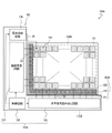
- FIG. 1 is a diagram schematically showing an exemplary configuration of an imaging device.
- FIG. 2 is a diagram schematically showing an exemplary circuit configuration of the imaging device.
- FIG. 3 is a schematic cross-sectional view showing a pixel area, a peripheral area, and a blocking area.
- FIG. 4 is a schematic plan view showing another example of the shape of the blocking area.
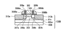
- FIG. 5 is a cross-sectional view showing a transistor according to the first configuration example.
- FIG. 6 is a cross-sectional view showing a transistor according to a first modification of the first configuration example.
- FIG. 7 is a cross-sectional view showing a transistor according to a second modification of the first configuration example.
- FIG. 1 is a diagram schematically showing an exemplary configuration of an imaging device.
- FIG. 2 is a diagram schematically showing an exemplary circuit configuration of the imaging device.
- FIG. 3 is a schematic cross-sectional view showing a pixel area, a peripheral area, and a blocking area.
- FIG. 8 is a diagram showing an impurity profile in the depth direction in the source/drain formation region according to the third modification of the first configuration example.
- FIG. 9 is a cross-sectional view showing a method of manufacturing a transistor according to the first configuration example.
- FIG. 10 is a cross-sectional view showing a method of manufacturing a transistor according to the first configuration example.
- FIG. 11 is a cross-sectional view showing a method of manufacturing a transistor according to the first configuration example.
- FIG. 12 is a graph showing an impurity profile in the depth direction in the extension formation region according to the first configuration example.
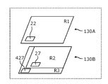
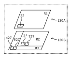
- FIG. 13 is a schematic perspective view illustrating transistors in a pixel region and transistors in a peripheral region.
- FIG. 14 is a schematic perspective view illustrating transistors in a pixel region and transistors in a peripheral region.
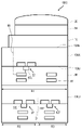
- FIG. 15 is a schematic cross-sectional view showing transistors in a pixel region and transistors in a peripheral region.
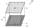
- FIG. 16 is a schematic perspective view illustrating transistors in a pixel region and transistors in a peripheral region.
- FIG. 17 is a schematic perspective view illustrating transistors in a pixel region and transistors in a peripheral region.
- FIG. 18 is a schematic perspective view illustrating transistors in a pixel region and transistors in a peripheral region.
- FIG. 19 is a schematic perspective view illustrating transistors in a pixel region and transistors in a peripheral region.
- FIG. 19 is a schematic perspective view illustrating transistors in a pixel region and transistors in a peripheral region.
- FIG. 20 is a schematic cross-sectional view showing transistors in a pixel region and transistors in a peripheral region.
- FIG. 21 is a schematic perspective view illustrating transistors in a pixel region and transistors in a peripheral region.
- FIG. 22 is a schematic perspective view illustrating transistors in a pixel region and transistors in a peripheral region.
- FIG. 23 is a schematic cross-sectional view showing transistors in a pixel region and transistors in a peripheral region.
- FIG. 24 is a schematic cross-sectional view showing transistors in a pixel region and transistors in a peripheral region.
- FIG. 25 is a schematic diagram of a back-illuminated imaging device.
- FIG. 26 is a schematic diagram of a back-illuminated imaging device.
- FIG. 27 is a schematic diagram of a back-illuminated imaging device.
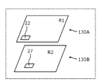
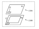
- FIG. 28 is a schematic diagram showing possible shapes of a pixel region and a peripheral region of an imaging device.
- FIG. 29 is a schematic diagram showing possible shapes of a pixel region and a peripheral region of an imaging device.
- FIG. 30 is a schematic diagram showing possible shapes of a pixel region and a peripheral region of an imaging device.
- FIG. 31 is a schematic diagram showing possible shapes of a pixel region and a peripheral region of an imaging device.
- FIG. 32 is a schematic diagram showing possible shapes of a pixel region and a peripheral region of an imaging device.
- FIG. 33A is a schematic cross-sectional view of an imaging device according to a specific example.
- FIG. 33A is a schematic cross-sectional view of an imaging device according to a specific example.
- FIG. 33B is a schematic perspective view of an imaging device according to a specific example
- FIG. 34A is a schematic cross-sectional view of an imaging device according to a specific example.
- FIG. 34B is a schematic perspective view of an imaging device according to a specific example;
- FIG. 35A is a schematic cross-sectional view of an imaging device according to a specific example.
- FIG. 35B is a schematic perspective view of an imaging device according to a specific example;
- FIG. 36A is a schematic cross-sectional view of an imaging device according to a specific example.
- FIG. 36B is a schematic perspective view of an imaging device according to a specific example;
- FIG. 37A is a schematic cross-sectional view of an imaging device according to a specific example.
- FIG. 37B is a schematic perspective view of an imaging device according to a specific example;
- FIG. 38 is a schematic cross-sectional view of an imaging device according to a specific example.
- the first layer may be heated for the following reasons. First, the first layer can be heated from the heat supplied in forming the first layer. Second, if the first and second layers are formed separately and then joined together, the heating for joining may heat the first layer. Third, when heat treatment of the second layer is performed after forming a laminated structure including the first layer and the second layer, the heat treatment may also heat the first layer.
- An imaging device that has a pixel region including pixel transistors and a peripheral region including peripheral transistors.
- the inventors have studied an imaging device in which a pixel substrate portion provided with pixel transistors and a peripheral substrate portion provided with peripheral transistors are stacked. Also in the manufacturing process of such an imaging device, the peripheral area may be heated for the same reason as described above. However, when the peripheral transistor is heated, conductive impurities may diffuse in the peripheral transistor. Diffusion of conductivity type impurities can degrade the performance of peripheral transistors. Degradation of the performance of peripheral transistors can degrade the performance of the imaging device as a whole. Therefore, the inventors have studied how to improve the performance of the imaging device, taking into consideration the existence of the peripheral transistors.
- An imaging device includes: a pixel region including a pixel substrate portion and an amplifying transistor provided in the pixel substrate portion for outputting a signal voltage corresponding to the amount of signal charge; A first peripheral region including a first peripheral substrate portion and at least one first peripheral transistor provided on the first peripheral substrate portion.
- the pixel substrate portion and the first peripheral substrate portion are stacked on each other.
- at least one type of impurity that contributes to suppression of transient enhanced diffusion of conductivity-type impurities is defined as a specific species
- the at least one first peripheral transistor includes a first specific layer located within the first peripheral substrate portion and containing a conductive impurity and the specific species.
- the technique according to the first aspect is suitable for improving the performance of the imaging device considering the existence of the first peripheral transistors in the first peripheral region.
- the specific species may contain at least one selected from the group consisting of carbon, nitrogen and fluorine.
- the specific species of the second aspect can suppress transient enhanced diffusion of conductive impurities.
- the specific species may contain at least one selected from the group consisting of germanium, silicon and argon.
- the specific species of the third aspect can suppress transient enhanced diffusion of conductive impurities by preamorphization.
- a gate length of the at least one first peripheral transistor may be shorter than a gate length of the amplification transistor.
- the configuration of the fourth aspect is an example of the configuration of the imaging device.
- the amplification transistor may include an amplification gate insulating film
- the at least one first peripheral transistor may include a first peripheral gate insulating film
- the first peripheral gate insulating film may be thinner than the amplification gate insulating film.
- the configuration of the fifth aspect is an example of the configuration of the imaging device.
- the at least one first peripheral transistor may include a first source, a first drain and a first extension diffusion layer;
- the first extension diffusion layer may be adjacent to the first source or the first drain and shallower than the first source and the first drain,
- the first extension diffusion layer may include the first specific layer.
- the configuration of the sixth aspect is an example of the configuration of the imaging device.
- the at least one first peripheral transistor may include a first source, a first drain and a first pocket diffusion layer; the first pocket diffusion layer may be adjacent to the first source or the first drain; The first pocket diffusion layer may include the first specific layer.
- the configuration of the seventh aspect is an example of the configuration of the imaging device.
- the at least one first peripheral transistor may comprise a first source and a first drain; At least one selected from the group consisting of the first source and the first drain may include the first specific layer.
- the configuration of the eighth aspect is an example of the configuration of an imaging device.
- the pixel substrate portion may include a charge accumulation region, which is an impurity region in which charges generated by photoelectric conversion are accumulated,
- the concentration of carbon in the first specific layer may be higher than the concentration of carbon in the charge storage region.
- the feature of the ninth aspect can be possessed by a high-performance imaging device.
- the amplifying transistor includes a gate;
- the concentration of carbon in the first specific layer may be higher than the concentration of carbon in a portion of the surface of the pixel substrate portion that overlaps the gate in plan view.
- the feature of the tenth aspect can be possessed by a high-performance imaging device.
- the pixel region may further include a photoelectric conversion layer, The photoelectric conversion layer, the pixel substrate portion, and the first peripheral substrate portion may be stacked on each other.
- the configuration of the eleventh aspect is an example of the configuration of an imaging device.
- the pixel substrate section may include a photodiode.
- the configuration of the twelfth aspect is an example of the configuration of an imaging device.
- the at least one first peripheral transistor may include an end-of-range defect; At least part of the first specific layer may be located above the end of range defect and may overlap with the end of range defect in plan view.
- the end-of-range defects of the thirteenth aspect can be traces of preamorphization that can enhance the effect of suppressing the diffusion of conductive impurities by impurities exemplified by carbon.
- the at least one first peripheral transistor may include a segregation portion in which the specific species are segregated in the depth direction of the first peripheral substrate portion, At least part of the first specific layer may be positioned above the segregation portion and may overlap the segregation portion in plan view.
- the segregation part of the fourteenth aspect can be traces of pre-amorphization that can enhance the effect of suppressing the diffusion of conductive impurities by impurities exemplified by carbon.
- the pixel substrate portion may include a charge accumulation region, which is an impurity region in which charges generated by photoelectric conversion are accumulated,
- the segregation portion may be shallower than the charge accumulation region.
- the configuration of the fifteenth aspect is an example of the configuration of an imaging device.
- the at least one first peripheral transistor may include two first peripheral transistors;
- the first peripheral substrate portion may include a shallow trench isolation structure,
- the shallow trench isolation structure may isolate the two first peripheral transistors,
- the shallow trench isolation structure may include trenches,
- a distribution range of the specific species in the first specific layer of at least one of the two first peripheral transistors may be a range shallower than the bottom of the trench.
- the configuration of the 16th aspect is an example of the configuration of the imaging device.
- the imaging device may further include an insulating section, The pixel substrate portion and the first peripheral substrate portion may be laminated via the insulating portion.
- the configuration of the 17th aspect is an example of the configuration of an imaging device.
- the imaging device includes a second peripheral board portion and at least one second peripheral provided on the second peripheral board portion. and a second peripheral region including a transistor,
- the first peripheral substrate portion and the second peripheral substrate portion may be included in one semiconductor substrate.
- the configuration of the eighteenth aspect is an example of the configuration of an imaging device.
- the imaging device includes a second peripheral substrate portion and at least one second peripheral provided on the second peripheral substrate portion. and a second peripheral region having a transistor, The pixel substrate portion, the first peripheral substrate portion, and the second peripheral substrate portion may be stacked on each other.
- the configuration of the 19th aspect is an example of the configuration of an imaging device.
- the imaging device includes a second peripheral board portion and at least one second peripheral provided on the second peripheral board portion.
- the pixel substrate portion may be included in the first semiconductor substrate,
- the first peripheral substrate portion may include a portion included in the second semiconductor substrate and a portion included in the third semiconductor substrate,
- the second peripheral substrate portion may include a portion included in the second semiconductor substrate and a portion included in the third semiconductor substrate,
- the at least one first peripheral transistor may include a P-channel transistor provided on the second semiconductor substrate and an N-channel transistor provided on the third semiconductor substrate;
- the at least one second peripheral transistor may include a P-channel transistor provided on the second semiconductor substrate and an N-channel transistor provided on the third semiconductor substrate;
- the first semiconductor substrate, the second semiconductor substrate and the third semiconductor substrate may be stacked on each other.
- the configuration of the twentieth aspect is an example of the configuration of an imaging device.
- the imaging device includes a second peripheral board portion and at least one second peripheral provided on the second peripheral board portion. and a second peripheral region including a transistor,
- the pixel substrate portion and the second peripheral substrate portion may be included in one semiconductor substrate.
- the configuration of the 21st aspect is an example of the configuration of an imaging device.
- the imaging device according to the 21st aspect may further include a vertical signal line, the at least one second peripheral transistor may comprise a load transistor; The amplification transistor may be connected to the load transistor via the vertical signal line.
- the configuration of the 22nd aspect is an example of the configuration of the imaging device.
- the at least one first peripheral transistor may include a first source, a first drain and a first extension diffusion layer;
- the first extension diffusion layer may be adjacent to the first source or the first drain and shallower than the first source and the first drain,
- the at least one second peripheral transistor may include a second source, a second drain and a second extension diffusion layer;
- the second extension diffusion layer may be adjacent to the second source or the second drain and shallower than the second source and the second drain,
- the concentration of the conductivity type impurity in the second extension diffusion layer may be lower than the concentration of the conductivity type impurity in the first extension diffusion layer,
- the second extension diffusion layer may be deeper than the first extension diffusion layer.
- the configuration of the twenty-third aspect is an example of the configuration of an imaging device.
- a gate length of the at least one first peripheral transistor may be shorter than a gate length of the at least one second peripheral transistor.
- the configuration of the twenty-fourth aspect is an example of the configuration of an imaging device.
- a gate length of the amplification transistor may be longer than a gate length of the at least one second peripheral transistor.
- the configuration of the twenty-fifth aspect is an example of the configuration of an imaging device.
- the at least one second peripheral transistor may include a second specific layer located in the second peripheral substrate portion and containing a conductivity type impurity, A concentration of the specific species in the first specific layer may be higher than a concentration of the specific species in the second specific layer.
- the configuration of the twenty-sixth aspect is an example of the configuration of an imaging device.
- the amplifying transistor may include a gate;
- the at least one second peripheral transistor may include a second specific layer located in the second peripheral substrate portion and containing a conductivity type impurity, The concentration of carbon in the second specific layer may be higher than the concentration of carbon in a portion of the surface of the pixel substrate portion that overlaps the gate in plan view.
- the configuration of the twenty-seventh aspect is an example of the configuration of an imaging device.
- the at least one second peripheral transistor may include a second source, a second drain and a second extension diffusion layer;
- the second extension diffusion layer may be adjacent to the second source or the second drain and shallower than the second source and the second drain,
- the second extension diffusion layer may include the second specific layer.
- the configuration of the twenty-eighth aspect is an example of the configuration of an imaging device.
- the at least one second peripheral transistor may include a second source, a second drain and a second pocket diffusion layer adjacent to the second source or the second drain;
- the second pocket diffusion layer may include the second specific layer.
- the configuration of the twenty-ninth aspect is an example of the configuration of an imaging device.
- the at least one second peripheral transistor may comprise a second source and a second drain; At least one selected from the group consisting of the second source and the second drain may include the second specific layer.
- the configuration of the thirtieth aspect is an example of the configuration of an imaging device.
- the at least one second peripheral transistor may include a second source, a second drain and a second extension diffusion layer;
- the second extension diffusion layer may be adjacent to the second source or the second drain and shallower than the second source and the second drain,
- the second extension diffusion layer may contain nitrogen.
- the configuration of the thirty-first aspect is an example of the configuration of the second peripheral transistor.
- the at least one second peripheral transistor may comprise an N-channel transistor.
- the reliability of the imaging device can be improved.
- the at least one first peripheral transistor may include a first peripheral gate insulating film; the at least one second peripheral transistor may include a second peripheral gate insulating film; The first peripheral gate insulating film may be thinner than the second peripheral gate insulating film.
- the configuration of the thirty-third aspect is an example of the configuration of an imaging device.
- the amplification transistor may include an amplification gate insulating film
- the at least one second peripheral transistor may include a second peripheral gate insulating film
- the amplification gate insulating film may be thicker than the second peripheral gate insulating film.
- the configuration of the thirty-fourth aspect is an example of the configuration of an imaging device.
- the imaging device may be a surface-illuminated imaging device,
- the pixel substrate portion may be arranged above the first peripheral substrate portion, the at least one first peripheral transistor may include a first gate electrode;
- the first gate electrode may be positioned above the first peripheral substrate portion.
- the configuration of the thirty-fifth aspect is an example of the configuration of an imaging device.
- the imaging device may be a back-illuminated imaging device,
- the pixel substrate portion may be arranged above the first peripheral substrate portion, the at least one first peripheral transistor may include a first gate electrode;
- the first gate electrode may be positioned below the first peripheral substrate portion.
- the configuration of the thirty-sixth aspect is an example of the configuration of an imaging device.
- the imaging device may be a surface-illuminated imaging device,
- the pixel substrate portion may be arranged below the first peripheral substrate portion, the at least one first peripheral transistor may include a first gate electrode;
- the first gate electrode may be positioned above the first peripheral substrate portion.
- the configuration of the thirty-seventh aspect is an example of the configuration of an imaging device.
- the imaging device may be a back-illuminated imaging device,
- the pixel substrate portion may be arranged below the first peripheral substrate portion, the at least one first peripheral transistor may include a first gate electrode;
- the first gate electrode may be positioned below the first peripheral substrate portion.
- the configuration of the thirty-eighth aspect is an example of the configuration of an imaging device.
- a manufacturing method includes: A method for manufacturing an imaging device according to any one of the first to thirty-eighth aspects, fabricating a laminated structure including the pixel substrate portion and the first peripheral substrate portion; heating the pixel substrate portion in the laminated structure.
- the manufacturing method of the thirty-ninth aspect is an example of a manufacturing method of an imaging device.
- the imaging device includes a pixel region including a pixel substrate portion and an amplifying transistor provided in the pixel substrate portion for outputting a signal voltage corresponding to the amount of signal charge; a first peripheral region including a first peripheral substrate portion and at least one first peripheral transistor provided on the first peripheral substrate portion; The pixel substrate portion and the first peripheral substrate portion are laminated to each other, When at least one impurity containing at least one selected from the group consisting of carbon, nitrogen and fluorine is defined as a specific species, The at least one first peripheral transistor includes a first specific layer located within the first peripheral substrate portion and containing a conductive impurity and the specific species.
- An imaging device includes: a pixel region including a pixel substrate portion and an amplifying transistor provided in the pixel substrate portion for outputting a signal voltage corresponding to the amount of signal charge; a first peripheral region including a first peripheral substrate portion and at least one first peripheral transistor provided on the first peripheral substrate portion; The pixel substrate portion and the first peripheral substrate portion are laminated to each other, When at least one impurity containing at least one selected from the group consisting of germanium, silicon and argon is defined as a specific species, The at least one first peripheral transistor includes a first specific layer located within the first peripheral substrate portion and containing a conductive impurity and the specific species.
- An imaging device includes: a pixel region including a pixel substrate portion and an amplifying transistor provided in the pixel substrate portion for outputting a signal voltage corresponding to the amount of signal charge; a first peripheral region including a first peripheral substrate portion and at least one first peripheral transistor provided on the first peripheral substrate portion; The pixel substrate portion and the first peripheral substrate portion are laminated to each other, the at least one first peripheral transistor includes a first source, a first drain and a first extension diffusion layer; the first extension diffusion layer is adjacent to the first source or the first drain and is shallower than the first source and the first drain; The first extension diffusion layer contains a first impurity and carbon.
- An imaging device includes: a pixel region including a pixel substrate portion and an amplifying transistor provided in the pixel substrate portion for outputting a signal voltage corresponding to the amount of signal charge; a first peripheral region including a first peripheral substrate portion and at least one first peripheral transistor provided on the first peripheral substrate portion; The pixel substrate portion and the first peripheral substrate portion are laminated to each other, the at least one first peripheral transistor includes a first source and a first drain; At least one selected from the group consisting of the first source and the first drain contains first impurities and carbon.
- the first extension diffusion layer may contain at least one selected from the group consisting of nitrogen, fluorine, germanium, silicon and argon instead of carbon or together with carbon.
- the first source or the first drain may contain at least one selected from the group consisting of nitrogen, fluorine, germanium, silicon and argon instead of or together with carbon.
- the first impurity is an impurity having conductivity. For the first impurity, the description regarding the conductivity type impurity described later can be applied.
- the "first impurity" can be read as the "conductivity-type impurity”.
- "carbon” can be read as "at least one type of impurity that contributes to suppression of transient enhanced diffusion of the first impurity".
- An imaging device includes: a pixel region including a pixel substrate portion and an amplifying transistor provided in the pixel substrate portion for outputting a signal voltage corresponding to the amount of signal charge; a first peripheral region including a first peripheral substrate portion and at least one first peripheral transistor provided on the first peripheral substrate portion; The pixel substrate portion and the first peripheral substrate portion are laminated to each other, The at least one first peripheral transistor includes a High-k metal gate.
- the operating voltage of the first peripheral transistor may be lower than the operating voltage of the second peripheral transistor.
- the threshold voltage of the first peripheral transistor may be smaller than the threshold voltage of the second peripheral transistor.
- plan view means when viewed from a direction perpendicular to the first semiconductor substrate, the second semiconductor substrate, the third semiconductor substrate, the pixel substrate portion, the first peripheral substrate portion, or the second peripheral substrate portion.
- the substrate may have a single layer structure or a laminated structure.
- a laminated structure may include, for example, a semiconductor layer, an insulating layer, and the like.
- the substrate may be a wafer obtained by slicing an ingot, or a film deposited by sputtering or the like.
- the substrate can be a plate-like body used in a chip stack structure.
- the substrate may be a plate-like body used in a laminated structure manufactured by 3DSI (3D Sequential Integration), which is a three-dimensional lamination technology called Sequential 3D.
- the extension diffusion layer is a concept including a so-called LDD (Lightly Doped Drain) diffusion layer.
- the gate length of the peripheral transistor is shorter than the gate length of the pixel transistor.
- "at least one" can be supplemented such that the gate length of at least one peripheral transistor is less than the gate length of at least one pixel transistor.
- FIG. 1 schematically illustrates an exemplary configuration of an imaging device according to certain embodiments of the present disclosure.
- the imaging device 100A shown in FIG. 1 has, for example, a plurality of pixels 110 arranged in a plurality of rows and columns.
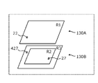
- the pixels 110 are arranged in m rows and n columns to form a substantially rectangular pixel region R1.
- m and n independently represent an integer of 1 or more.
- each of these pixels 110 includes a photoelectric conversion portion supported by the semiconductor substrate 130A and a readout portion formed on the semiconductor substrate 130A and electrically connected to the photoelectric conversion portion. circuit.
- each of the plurality of pixels 110 is an impurity region provided in the semiconductor substrate 130A, and serves as a charge accumulation region that temporarily holds signal charges generated by the photoelectric conversion unit. An impurity region functioning as part of the region is included.
- a photodiode may be provided in the semiconductor substrate as the photoelectric conversion section.
- the imaging device 100A further has a peripheral circuit 120A that drives the plurality of pixels 110.
- the peripheral circuit 120A includes a vertical scanning circuit 122, a horizontal signal reading circuit 124, a voltage supply circuit 126 and a control circuit 128. In embodiments of the present disclosure, some or all of these circuits are formed on the semiconductor substrate 130B.
- the peripheral circuit 120A is located in a first peripheral region R2 provided on the semiconductor substrate 130B. Note that FIG. 1 shows both the semiconductor substrates 130A and 130B for convenience of explanation. In practice, the semiconductor substrate 130A and the semiconductor substrate 130B are laminated together. Specifically, the semiconductor substrate 130A and the semiconductor substrate 130B are stacked with an interlayer insulating layer 90B interposed therebetween.
- the imaging device 100A further has a blocking area 200A provided outside the pixel area R1 in plan view.
- the blocking region 200A includes an impurity region 131 formed in a semiconductor substrate 130A and a plurality of contact plugs 211 provided on the impurity region 131.
- Impurity region 131 is typically a P-type diffusion region.
- the plurality of contact plugs 211 are electrically connected to the impurity regions 131 of the semiconductor substrate 130A by being provided on the impurity regions 131 .
- the plurality of contact plugs 211 are configured to be able to supply a predetermined voltage to the impurity regions 131 by being connected to a power source (not shown in FIG. 1). That is, during operation of the imaging device 100A, the impurity region 131 is in a state where a predetermined voltage is applied via the contact plug 211.
- the blocking region 200A has an element isolation 220 .
- the element isolation 220 is a structure formed in the semiconductor substrate 130A by, for example, an STI (shallow trench isolation) process.
- the element isolation 220 can be provided in the semiconductor substrate 130A so as to surround the pixel region R1 when viewed from above.
- the element isolation 220 corresponds to the shallow trench isolation structure in this disclosure. Note that the blocking region 200A is not essential.
- the vertical scanning circuit 122 has connections with a plurality of address signal lines 34 . These address signal lines 34 are provided corresponding to each row of the plurality of pixels 110 . Each address signal line 34 is connected to one or more pixels 110 belonging to the corresponding row.
- the vertical scanning circuit 122 controls the timing of reading out signals from the pixels 110 to vertical signal lines 35 to be described later by applying row selection signals to the address signal lines 34 .
- the vertical scanning circuit 122 is also called a row scanning circuit.
- a signal line connected to the vertical scanning circuit 122 is not limited to the address signal line 34 .
- a plurality of types of signal lines can be connected to the vertical scanning circuit 122 for each row of the plurality of pixels 110 .
- the imaging device 100A also has a plurality of vertical signal lines 35.
- a vertical signal line 35 is provided for each column of the plurality of pixels 110 .
- Each vertical signal line 35 is connected to one or more pixels 110 belonging to the corresponding column.
- These vertical signal lines 35 are connected to the horizontal signal readout circuit 124 .
- the horizontal signal readout circuit 124 sequentially outputs the signals read out from the pixels 110 to output lines (not shown in FIG. 1).
- the horizontal signal readout circuit 124 is also called a column scanning circuit.
- the control circuit 128 receives command data, clocks, etc. given from the outside of the imaging device 100A, for example, and controls the entire imaging device 100A.
- the control circuit 128 typically has a timing generator and supplies drive signals to the vertical scanning circuit 122, the horizontal signal readout circuit 124, the voltage supply circuit 126 described later, and the like. Arrows extending from the control circuit 128 in FIG. 1 schematically represent the flow of output signals from the control circuit 128 .
- Control circuitry 128 may be implemented, for example, by a microcontroller including one or more processors.
- the functions of the control circuit 128 may be realized by a combination of a general-purpose processing circuit and software, or by hardware specialized for such processing.
- the peripheral circuit 120A includes a voltage supply circuit 126 electrically connected to each pixel 110 in the pixel region R1.
- a voltage supply circuit 126 supplies a predetermined voltage to the pixels 110 via the voltage line 38 .
- the voltage supply circuit 126 is not limited to a specific power supply circuit, and may be a circuit that converts voltage supplied from a power source such as a battery into a predetermined voltage, or a circuit that generates a predetermined voltage. good.
- the voltage supply circuit 126 may be part of the vertical scanning circuit 122 described above. As schematically shown in FIG. 1, these circuits forming the peripheral circuit 120A are arranged in the first peripheral region R2.
- the number and arrangement of the pixels 110 are not limited to the illustrated example.
- the number of pixels 110 included in the imaging device 100A may be one.
- the center of each pixel 110 is positioned on a lattice point of a square lattice. 110 may be placed.
- the pixels 110 may be arranged one-dimensionally, in which case the imaging device 100A can be used as a line sensor.
- FIG. 2 schematically shows an exemplary circuit configuration of the imaging device 100A shown in FIG.
- four pixels 110 arranged in 2 rows and 2 columns are extracted and shown among the plurality of pixels 110 in order to avoid overcomplicating the drawing.
- Each of these pixels 110 includes a photoelectric conversion section 10 and a readout circuit 20 electrically connected to the photoelectric conversion section 10 .
- the photoelectric conversion section 10 includes a photoelectric conversion layer arranged above the semiconductor substrate 130A.
- the photoelectric conversion unit 10 of each pixel 110 is connected to the voltage line 38 connected to the voltage supply circuit 126, so that a predetermined voltage can be applied through the voltage line 38 during operation of the imaging device 100A.
- a predetermined voltage can be applied through the voltage line 38 during operation of the imaging device 100A.
- a positive voltage of about 10 V for example, can be applied to the voltage line 38 during operation of the imaging device 100A.
- holes are used as signal charges will be exemplified below.
- the read circuit 20 includes an amplification transistor 22, an address transistor 24 and a reset transistor 26.
- the amplification transistor 22, the address transistor 24 and the reset transistor 26 are typically field effect transistors formed on the semiconductor substrate 130A.
- MOSFET Metal Oxide Semiconductor Field Effect Transistor
- the gate of the amplification transistor 22 is electrically connected to the photoelectric conversion section 10 .
- the charge accumulation node FD is a node that connects the gate of the amplification transistor 22 to the photoelectric conversion section 10 .
- the charge accumulation node FD has a function of temporarily holding charges generated by the photoelectric conversion unit 10 .
- Charge storage node FD partially includes an impurity region formed in semiconductor substrate 130A.
- the drain of the amplification transistor 22 of each pixel 110 is connected to the power supply wiring 32 .
- the power supply wiring 32 supplies a power supply voltage VDD of about 3.3 V, for example, to the amplification transistor 22 during operation of the imaging device 100A.
- the source of the amplification transistor 22 is connected to the vertical signal line 35 via the address transistor 24 .
- the amplifying transistor 22 outputs a signal voltage corresponding to the amount of signal charge accumulated in the charge accumulation node FD by receiving the power supply voltage VDD at its drain.
- An address signal line 34 is connected to the gate of the address transistor 24 connected between the amplification transistor 22 and the vertical signal line 35 .
- the vertical scanning circuit 122 controls on/off of the address transistor 24 by applying a row selection signal to the address signal line 34 . That is, the vertical scanning circuit 122 can read out the output of the amplification transistor 22 of the selected pixel 110 to the corresponding vertical signal line 35 by controlling the row selection signal. Note that the arrangement of the address transistor 24 is not limited to the example shown in FIG.
- a load circuit 45 and a column signal processing circuit 47 are connected to each of the vertical signal lines 35 .
- the load circuit 45 forms a source follower circuit together with the amplification transistor 22 .
- the column signal processing circuit 47 performs noise suppression signal processing typified by correlated double sampling, analog-to-digital conversion, and the like.
- the column signal processing circuit 47 is also called a row signal storage circuit.
- the horizontal signal readout circuit 124 sequentially reads signals from the plurality of column signal processing circuits 47 to the horizontal common signal line 49 .
- Column signal processing circuitry 47 may be part of horizontal signal readout circuitry 124 .
- Load circuit 45 and column signal processing circuit 47 may be part of peripheral circuit 120A described above.
- the readout circuit 20 includes a reset transistor 26 in addition to the amplification transistor 22 and the address transistor 24 .
- One of the drain and source of the reset transistor 26 is part of the charge storage node FD, and the other of the drain and source is connected to the reset voltage line 39 .
- the one of the drain and the source of the reset transistor 26 corresponds to the charge accumulation region Z in FIG. 3, specifically the impurity region 60n.
- the reset voltage line 39 is connected to a reset voltage supply circuit (not shown in FIG. 2) so that a predetermined reset voltage Vref can be supplied to the reset transistor 26 of each pixel 110 during operation of the imaging device 100A. .
- the reset voltage Vref for example, 0V or a voltage near 0V is selected.
- the reset voltage supply circuit may apply a predetermined reset voltage Vref to the reset voltage line 39, and its specific configuration is not limited to a specific power supply circuit.
- the reset voltage supply circuit may be part of the vertical scanning circuit 122 .
- the voltage supply circuit 126 and the reset voltage supply circuit may be independent separate circuits, or may be arranged in the imaging device 100A in the form of a single voltage supply circuit.
- a reset voltage supply circuit may also be part of the peripheral circuit 120A described above.
- a reset signal line 36 is connected to the gate of the reset transistor 26 .
- the reset signal line 36 is provided for each row of the plurality of pixels 110 similarly to the address signal line 34 and is connected to the vertical scanning circuit 122 here.
- the vertical scanning circuit 122 can select the pixels 110 from which signals are to be read out on a row-by-row basis by applying row selection signals to the address signal lines 34 .
- the vertical scanning circuit 122 can turn on the reset transistors 26 in the selected row by applying a reset signal to the gates of the reset transistors 26 via the reset signal line 36 .
- the potential of the charge storage node FD is reset by turning on the reset transistor 26 .
- FIG. 3 is a schematic cross-sectional view showing the pixel region R1, the first peripheral region R2 and the blocking region.
- cross sections of two pixels are shown as representatives of the plurality of pixels 110 .
- the semiconductor substrate 130A and the semiconductor substrate 130B are laminated together. Specifically, the semiconductor substrate 130A and the semiconductor substrate 130B are stacked with an interlayer insulating layer 90B interposed therebetween.
- a photoelectric conversion layer 12 is provided in the pixel region R1.
- the photoelectric conversion layer 12 is supported by the semiconductor substrate 130A.
- a translucent counter electrode 13 is arranged on the photoelectric conversion layer 12 .
- each of the photoelectric conversion layer 12 and the counter electrode 13 is typically provided continuously above the semiconductor substrate 130A over the plurality of pixels 110.
- FIG. 1 shows that the photoelectric conversion layer 12 and the counter electrode 13 is typically provided continuously above the semiconductor substrate 130A over the plurality of pixels 110.
- the pixel 110 is a unit structure that configures the pixel region R1, and includes a photoelectric conversion section 10 having a portion of the photoelectric conversion layer 12, a portion of the counter electrode 13, and the pixel electrode 11.
- the pixel electrode 11 of the photoelectric conversion unit 10 is located between the photoelectric conversion layer 12 and the semiconductor substrate 130A, and is doped with a metal such as aluminum or copper, a metal nitride, or an impurity to provide conductivity. made of polysilicon or the like.
- the pixel electrode 11 of each pixel 110 is electrically isolated from the pixel electrodes 11 of other adjacent pixels by being spatially separated for each pixel.
- the photoelectric conversion layer 12 of the photoelectric conversion section 10 is made of an organic material or an inorganic material such as amorphous silicon.
- the photoelectric conversion layer 12 receives light incident through the counter electrode 13 and generates positive and negative charges through photoelectric conversion. That is, the photoelectric conversion unit 10 has a function of converting light into charge.
- the photoelectric conversion layer 12 may include a layer made of an organic material and a layer made of an inorganic material.
- the counter electrode 13 of the photoelectric conversion section 10 is an electrode made of a transparent conductive material such as ITO.
- the term “translucent” means that at least part of light having a wavelength that can be absorbed by the photoelectric conversion layer 12 is transmitted, and that light is transmitted over the entire wavelength range of visible light. is not required.
- the counter electrode 13 is connected to the voltage line 38 described above.
- the potential of the voltage line 38 to make the potential of the counter electrode 13 higher than the potential of the pixel electrode 11, for example, the positive charge and the negative charge generated by the photoelectric conversion are reduced. Charge can be selectively collected by the pixel electrode 11 .
- By forming the counter electrode 13 in the form of a continuous single layer over the plurality of pixels 110 it is possible to collectively apply a predetermined potential to the counter electrodes 13 of the plurality of pixels 110 via the voltage line 38. is.
- Each of the plurality of pixels 110 further includes a portion of the semiconductor substrate 130A.
- the semiconductor substrate 130A has a plurality of impurity regions 60n as first impurity regions near its surface.
- the impurity region 60n functions as one of the drain and source of the reset transistor 26 included in the readout circuit 20 described above.
- the semiconductor substrate 130A also has an impurity region 61n that is the other of the drain and source of the reset transistor 26.
- the impurity region 61n is connected to the reset voltage line 39 via a polysilicon plug or the like.
- the impurity regions 60n and 61n have N-type conductivity. These impurity regions 60n and 61n are typically N-type diffusion regions.
- a plurality of readout circuits 20 corresponding to a plurality of pixels 110 are formed on the semiconductor substrate 130A.
- the readout circuit 20 of each pixel is electrically isolated from the readout circuits 20 of other pixels by an element isolation 221 provided on the semiconductor substrate 130A.
- Interlayer insulating layer 90A covering the semiconductor substrate 130A is positioned between the photoelectric conversion section 10 and the semiconductor substrate 130A.
- Interlayer insulating layer 90A generally includes a plurality of insulating layers and a plurality of wiring layers.
- a plurality of wiring layers arranged in the interlayer insulating layer 90A includes a wiring layer having the address signal line 34 and the reset signal line 36 as part thereof, the vertical signal line 35, the power supply wiring 32, the reset voltage line 39 and the like.
- a wiring layer or the like included in a portion thereof may be included.
- the number of insulating layers and the number of wiring layers in the interlayer insulating layer 90A are not limited to this example and can be set arbitrarily.
- a conductive structure 89 for electrically connecting the pixel electrode 11 of the photoelectric conversion unit 10 to the readout circuit 20 formed on the semiconductor substrate 130A is provided inside the interlayer insulating layer 90A.
- the conductive structure 89 includes traces and vias located in the interlayer insulating layer 90A. These lines and vias are typically formed from metals such as copper or tungsten, or metal compounds such as metal nitrides or metal oxides.
- Conductive structure 89 also includes contact plug cx connected to impurity region 60n described above. Contact plug cx connected to impurity region 60n is typically a polysilicon plug doped with an impurity such as phosphorus to enhance conductivity.
- the conductive structure 89 also has an electrical connection with the gate electrode of the amplification transistor 22 .
- a plug cy is connected to the contact plug cx. Tungsten, copper and the like are exemplified as metals that the plug cy may contain.
- the semiconductor substrate 130A includes a support substrate 140A and one or more semiconductor layers formed on the support substrate 140A.
- the semiconductor substrate 130A has an N-type semiconductor layer 62an provided on the support substrate 140A.
- a P-type silicon substrate is exemplified as the support substrate 140A.
- the support substrate 140A may have a lower electrical resistivity than the N-type semiconductor layer 62an.
- the semiconductor substrate 130A may be an SOI (silicon-on-insulator) substrate, or a substrate having a semiconductor layer provided on its surface by epitaxial growth or the like. Note that semiconductor substrates 130B and 130C, which will be described later, can also have the same characteristics as the semiconductor substrate 130A.
- the semiconductor substrate 130A has an N-type semiconductor layer 62an on the support substrate 140A and a P-type semiconductor layer 63p on the N-type semiconductor layer 62an.
- the potential of the N-type semiconductor layer 62an is controlled via a well contact (not shown in FIG. 3).
- the semiconductor substrate 130A further includes a P-type semiconductor layer 66p located on the P-type semiconductor layer 63p and a P-type impurity region 65p formed in the P-type semiconductor layer 66p.
- the aforementioned impurity region 60n having connection with the conductive structure 89 is provided in a P-type impurity region 65p.
- a junction capacitance formed by a pn junction between the impurity region 60n and the P-type impurity region 65p serving as the P well functions as a capacitance that stores at least part of the signal charge collected by the pixel electrode 11.
- the impurity region 60n constitutes a charge accumulation region that temporarily holds signal charges.
- the impurity region 61n is provided in the P-type semiconductor layer 66p.
- the impurity concentration in the P-type impurity region 65p is lower than the impurity concentration in the P-type semiconductor layer 66p.
- the semiconductor substrate 130A also has a plurality of P-type regions 64 provided in the semiconductor substrate 130A so as to penetrate the N-type semiconductor layer 62an.
- P-type region 64 has a relatively high impurity concentration.
- the plurality of P-type regions 64 are arranged below the plurality of P-type regions 64a located in the pixel region R1 when viewed from the normal direction of the semiconductor substrate 130A and the plurality of contact plugs 211 in the blocking region 200A. and located one or more P-type regions 64b.
- the P-type region 64a is formed between the P-type semiconductor layer 63p and the support substrate 140A so as to penetrate the N-type semiconductor layer 62an, and has the function of electrically connecting the P-type semiconductor layer 63p and the support substrate 140A.
- the P-type region 64b is electrically connected to the impurity region 131 by reaching the impurity region 131 of the blocking region 200A at one end thereof, and electrically connects the impurity region 131 and the support substrate 140A.
- an electrical path is formed in the semiconductor substrate 130A from the impurity region 131 of the blocking region 200A to the P-type semiconductor layer 63p through the P-type region 64b, the support substrate 140A and the P-type region 64a.
- a plurality of contact plugs 211 are connected to the impurity region 131 of the blocking region 200A, and these contact plugs 211 are configured to be connectable to a power supply (not shown) such as ground.
- a power supply not shown
- the potential of the impurity region 131 in the blocking region 200A can be grounded through a plurality of contact plugs 211.
- the P-type semiconductor layer 100 is formed by using an electrical path including the impurity region 131, the P-type region 64b, the support substrate 140A and the P-type region 64a.
- the potentials of the P-type impurity region 65p and the P-type semiconductor layer 66p can be controlled via 63p.
- an impurity region 131a having a relatively high impurity concentration is formed in a portion of the impurity region 131 located near the surface of the semiconductor substrate 130A.
- Contact plug 211 is typically made of metal.
- a silicide layer 131s is formed between the multiple contact plugs 211 and the impurity regions 131 .
- the contact resistance can be further reduced.
- the first peripheral region R2 includes, for example, a plurality of transistors 25 and a first peripheral transistor 27 forming a logic circuit such as a multiplexer.
- a logic circuit such as a multiplexer.
- an N-type semiconductor layer 62bn is formed on a support substrate 140B, and an N-type impurity region 81n and a P-type impurity region 82p as wells are formed on the N-type semiconductor layer 62bn. and are formed.
- the drain and source of the transistor 25 are located in the P-type impurity region 82p, and the drain and source of the first peripheral transistor 27 are located in the N-type impurity region 81n.
- a predetermined voltage is supplied to the N-type semiconductor layer 62bn by connecting a power source (not shown).
- a P-type silicon substrate is exemplified as the support substrate 140B.
- the N-type impurity region 81n may be referred to as an N-type well.
- the depth of the N-type semiconductor layer 62an in the pixel region R1 and the depth of the N-type semiconductor layer 62bn in the first peripheral region R2 may be the same or different.
- contact plugs cp are connected to the drain, source, and gate electrodes of peripheral transistors such as the transistor 25 and the first peripheral transistor 27 .
- Each of the impurity layers and impurity regions located above the support substrate 140A is typically formed by ion implantation of impurities into the semiconductor layer obtained by epitaxial growth on the support substrate 140A.
- the P-type region 64a located in the pixel region R1 can be formed at a position that does not overlap with the element isolation in the pixel in plan view.
- each of the impurity layers and impurity regions located above the support substrate 140B is typically formed by ion implantation of impurities into the semiconductor layer obtained by epitaxial growth on the support substrate 140B.
- FIG. 4 shows another example of the shape of the blocking area.
- the imaging device 100B shown in FIG. 4 has a blocking region 200B that surrounds the pixel region R1 in a rectangular shape instead of the blocking region 200A.
- the impurity region 131 of the blocking region 200B surrounds the pixel region R1 in a ring shape without discontinuity in plan view.
- a plurality of contact plugs 211 are connected to the impurity region 131 also in this example.
- the element isolation 220 of the cutoff region 200B also surrounds the pixel region R1 in an annular shape inside the impurity region 131 without discontinuity.
- FIG. 4 shows another example of the shape of the blocking area.
- FIG. 4 shows both the semiconductor substrates 130A and 130B for convenience of explanation.
- the semiconductor substrate 130A and the semiconductor substrate 130B are laminated together.
- the semiconductor substrate 130A and the semiconductor substrate 130B are stacked with an interlayer insulating layer 90B interposed therebetween.
- the peripheral circuit 120B provided in the first peripheral region R2 includes a second vertical scanning circuit 129 and a second vertical scanning circuit 129. 2 horizontal signal readout circuits 127 are included. As illustrated, the vertical scanning circuit 129 is also connected to address signal lines 34 provided corresponding to each row of the plurality of pixels 110 .
- the vertical scanning circuit 122 performs the row selection operation of the pixels in the left half of the pixel region R1
- the vertical scanning circuit 129 performs the row selection operation of the pixels in the right half of the pixel region R1.
- the horizontal signal readout circuit 124 processes signals read out from pixels in the lower half of the pixel region R1
- the horizontal signal readout circuit 127 processes signals read out from pixels in the upper half of the pixel region R1. responsible for processing. In this way, by partitioning the pixel region R1 and reading out signals by a plurality of vertical scanning circuits and horizontal signal reading circuits, it is possible to increase the speed of operation such as shortening the frame rate.
- the shielding region 200B By forming the shielding region 200B in the semiconductor substrate 130A in a shape surrounding the pixel region R1 including the array of the plurality of pixels 110 in plan view, charge transfer between the charge accumulation region of the pixels and the outside of the pixel region R1 is prevented. It can be suppressed more effectively.
- the cut-off region continuously surrounds the pixel region R1 annularly in plan view.
- the blocking region may include a plurality of portions each including the element isolation 220 and the impurity region 131 and arranged to surround the pixel region R1 as a whole. In such a configuration as well, the same effect as in the case of providing a shielding region so as to surround the pixel region R1 in a ring shape without discontinuity in plan view can be expected.
- the blocking region 200B may be omitted.
- first peripheral region R2 includes first peripheral transistor 27 .
- first peripheral transistor 27 configuration examples of the first peripheral transistor 27 according to the embodiment will be described with reference to FIGS. 5 to 12.
- FIG. 5 shows a cross-sectional configuration of the first peripheral transistor 27 according to the first configuration example.
- the first peripheral transistor 27 is specifically a MIS transistor, more specifically a MOSFET.
- a gate insulating film 301 made of silicon oxide (SiO 2 ) is interposed, and polysilicon or metal gates are formed.
- a gate electrode 302 is formed.
- An N-type channel diffusion layer 303 diffused with, for example, arsenic (As) and an N-type channel diffusion layer 303 diffused with, for example, arsenic (As) and phosphorus (P) are formed above the semiconductor substrate 130B to have a junction depth greater than that of the N-type channel diffusion layer 303.
- a support substrate 140B, an N-type semiconductor layer 62bn, and an N-type impurity region 81n, which is an N-type well, are stacked in this order.
- First extension diffusion layers 306a and 306b which are extension high-concentration diffusion layers, and N-type pockets formed below the first extension diffusion layers 306a and 306b by diffusing an N-type impurity such as arsenic (As).
- First pocket diffusion layers 307a and 307b, which are diffusion layers, are formed.
- the first extension diffusion layers 306a and 306b which are P-type extension high-concentration diffusion layers, contain carbon (C).
- the first extension diffusion layers 306a and 306b have a shallow and steep impurity profile and maintain a high activation concentration.
- an extension diffusion layer having a shallow junction depth and a low resistance is formed, and a fine device having a high driving force can be realized.
- the first peripheral region R2 may be heated by heat in the manufacturing process of the imaging device.
- the conductivity type impurity is regenerated in the first peripheral transistor 27 in the first peripheral region R2. The distribution can be suppressed and shallow junctions can be maintained.
- a laminated structure may be obtained by forming a lower transistor layer and subsequently forming an upper transistor layer.
- the lower transistor layers are affected by the heat treatment of the upper transistor layers.
- the thermal resistance of the lower transistor layers By improving the thermal resistance of the lower transistor layers to account for the "extra" heat imparted to the lower transistor layers by the heat treatment of the upper transistor layers, it is possible to ensure the performance of the lower transistor layers.
- the stacked semiconductor device corresponds to the imaging device 100A
- the lower transistor layer corresponds to the first peripheral region R2
- the transistor in the lower transistor layer corresponds to the first peripheral transistor 27.
- the first peripheral transistor 27 in the first peripheral region R2 can be prevented from A shallow junction can be maintained by suppressing redistribution of conductivity type impurities.
- the first extension diffusion layers 306a and 306b contain carbon, the effect of suppressing the occurrence of residual defects in the first extension diffusion layers 306a and 306b can also be achieved.
- An example of a residual defect is an end of range (hereinafter abbreviated as EOR) defect.
- EOR defect is a defect layer formed in a region immediately below the amorphous crystal (a/c) interface before the heat treatment when the semiconductor substrate 130B made of silicon is heat-treated in an amorphous state. Say things.
- TED transient enhanced diffusion
- Carbon forms a composite of excess point defects that cause TED and carbon-interstitial silicon, clusters, etc., thereby suppressing excess point defects.
- excess point defects can grow and generate secondary defects such as dislocation loops, it can be said that carbon suppresses crystal defects.
- the crystal layer in which the formation of residual defect layers such as secondary defects is suppressed in the extension formation region of the semiconductor substrate 130B, the occurrence of junction leakage due to the residual defect layers is also suppressed. be able to.
- P-type electrodes are connected to the first extension diffusion layers 306a and 306b and have a deeper junction depth than the first extension diffusion layers 306a and 306b.
- a source diffusion layer 313a and a P-type drain diffusion layer 313b are formed.
- the P-type source diffusion layer 313a and the P-type drain diffusion layer 313b contain carbon (C).
- one or both of the P-type source diffusion layer 313a and the P-type drain diffusion layer 313b may not contain carbon (C).
- Insulating offset spacers 309a and 309b are formed on both side surfaces of the gate electrode 302, and the offset spacers 309a and 309b contain carbon. Further, the L-shaped cross section extends from the outer side surface of each of the offset spacers 309a and 309b to the upper part of the inner end of the P-type source diffusion layer 313a and the P-type drain diffusion layer 313b above the semiconductor substrate 130B. of first sidewalls 308Aa and 308Ab are formed. Insulating second sidewalls 308Ba and 308Bb are formed outside the first sidewalls 308Aa and 308Ab, respectively.
- arsenic ions are used as impurities in the N-type channel diffusion layer 303 in the first configuration example, ions of an element having a larger mass than arsenic ions and exhibiting N-type, or arsenic ions may be used instead of arsenic ions. and ions of an element having a larger mass than the arsenic ions and exhibiting N-type may be used.
- impurities that contribute to suppressing TED are not limited to carbon. At least one selected from the group consisting of nitrogen, fluorine, germanium, silicon and argon may be used in place of or together with carbon. Nitrogen, fluorine, germanium, silicon, argon, etc. can also contribute to TED suppression. Specifically, as with carbon, impurities such as nitrogen and fluorine also form excess point defects that cause TED and impurity-interstitial silicon or impurity-atom vacancy complexes, clusters, etc., thereby forming excess point defects. suppress Specifically, excess point defects are suppressed by forming complexes such as carbon-interstitial silicon, nitrogen-interstitial silicon, fluorine-interstitial silicon, and fluorine-atomic vacancies.
- Germanium, silicon, argon, etc. contribute to suppression of TED through pre-amorphization.
- at least one element selected from the group consisting of group 14, group 17, and group 18 elements having no conductivity may be used as an impurity that contributes to suppressing TED.
- a P-channel MIS transistor is used as a transistor, but an N-channel MIS transistor may be used instead.
- an N-channel MIS transistor for example, phosphorus (P) ions, arsenic (As) ions, antimony (Sb) ions, bismuth (Bi) ions, etc. are used as N-type impurity ions forming the extension diffusion layers.
- P phosphorus
- As arsenic
- Sb antimony
- Bi bismuth
- a group 5B element having a larger mass than the arsenic ion of the group 5B can be used.
- the P-type pocket diffusion layer is doped with, for example, boron (B) ions, group III elements having a larger mass than boron ions such as indium (In) ions, or a combination thereof. can be used.
- B boron
- group III elements having a larger mass than boron ions such as indium (In) ions, or a combination thereof. can be used.
- the TED of the P-type pocket diffusion layer is suppressed by carbon, so variations in threshold voltage caused by the pocket profile can be suppressed.
- the N-type impurity ions forming the extension diffusion layer one of the above impurities may be used, or two or more of them may be used in combination. The same applies to the elements used for the P-type pocket diffusion layer.
- FIG. 6 shows a cross-sectional configuration of a transistor according to a first modification of the first configuration example.
- the impurity profiles of the first extension diffusion layers 306a and 306b which are P-type extension high-concentration diffusion layers, are asymmetrical with respect to the gate electrode 302.
- the source region shallower and steeper than the drain region, the carrier concentration gradient between the source region and the channel region increases, and the driving force in the MIS transistor increases. improves.
- the transistor having the structure in FIG. 6 can be manufactured with reference to Patent Document 2, for example.
- the first extension diffusion layer 306a is shallower than the first extension diffusion layer 306b.
- a configuration in which the first extension diffusion layer 306b is shallower than the first extension diffusion layer 306a may also be adopted.
- FIG. 7 shows a cross-sectional configuration of a transistor according to a second modification of the first configuration example.
- the transistor according to the second modification has a P-type extension high-concentration diffusion layer only on one side of a P-type source diffusion layer 313a and a P-type drain diffusion layer 313b.
- the transistor according to the second modification has a first extension diffusion layer 306a which is a P-type extension high-concentration diffusion layer adjacent to the P-type source diffusion layer 313a. It does not have a first extension diffusion layer adjacent to the diffusion layer 313b. However, it is also possible to employ a configuration that does not have the first extension diffusion layer adjacent to the P-type source diffusion layer 313a and has the first extension diffusion layer 306b adjacent to the P-type drain diffusion layer 313b.
- the transistor according to the second modification has an N-type pocket diffusion layer only on one side of the P-type source diffusion layer 313a and the P-type drain diffusion layer 313b.
- the transistor according to the second modification has a first pocket diffusion layer 307a adjacent to the P-type source diffusion layer 313a, and a first pocket diffusion layer adjacent to the P-type drain diffusion layer 313b. does not have
- the P-type source diffusion layer 313a and the P-type drain diffusion layer 313b contain fluorine (F) and carbon (C). Fluorine can cause partial amorphization of the semiconductor substrate 130B. Fluorine can also suppress transient enhanced diffusion (TED) of impurities.
- FIG. 8 shows an example of concentration distribution of impurities in the P-type source diffusion layer 313a and the P-type drain diffusion layer 313b in the depth direction of the semiconductor substrate 130B. The vertical axis shows the concentration of fluorine (F), carbon (C), boron (B) and germanium (Ge) on a logarithmic scale. The concentration distribution of FIG.
- the fluorine concentration distribution has a segregation near the original a/c interface location.
- the diffusion of impurities is suppressed after the annealing. Further, even if the first peripheral region R2 is heated during the heat treatment for the pixel region R1, the redistribution of the conductive impurities can be kept within a small range.
- FIGS. 9 to 11 are cross-sectional views showing a method of manufacturing the transistor shown in FIG.
- description of the manufacturing method of the N-type semiconductor layer 62bn is omitted. Fabrication of the N-type semiconductor layer 62bn can be performed by a known method.
- Parts (a) to (e) of FIG. 9, parts (a) to (d) of FIG. 10, and parts (a) to (c) of FIG. 1 shows a cross-sectional configuration in the order of steps.
- N-type impurity ions such as phosphorus (P) ions
- P phosphorus
- a first ion implantation of 4 ⁇ 10 12 /cm 2 and a second ion implantation with an implantation energy of 540 keV and an implantation dose of 1 ⁇ 10 13 /cm 2 are performed to form an N-type well impurity implantation layer 304A. do.
- arsenic (As) ions are implanted into the semiconductor substrate 130B at an implantation energy of about 90 keV and an implantation dose of about 5 ⁇ 10 12 /cm 2 to form an N-type well impurity-implanted layer 304A above the N-type well impurity implantation layer 304A.
- a channel impurity-implanted layer 303A is formed.
- a silicon oxide film may be deposited on the surface of the semiconductor substrate 130B before ion implantation.
- the order of forming the N-type well impurity-implanted layer 304A and the N-type channel impurity-implanted layer 303A is not particularly limited.
- the ion-implanted semiconductor substrate 130B is heated from 850° C. to 1050° C. at a temperature elevation rate of about 100° C./sec or more, for example, about 200° C./sec.
- a first rapid thermal process is performed by either holding the peak temperature for up to about 10 seconds or not holding the peak temperature.
- an N-type channel diffusion layer 303 and an N-type impurity region 81n, which is an N-type well are formed above the semiconductor substrate 130B.
- the rapid heat treatment that does not hold the peak temperature refers to heat treatment in which the heat treatment temperature is lowered as soon as it reaches the peak temperature.
- a gate insulating film 301 made of silicon oxide with a film thickness of about 1.5 nm is formed on the semiconductor substrate 130B, and a poly film with a film thickness of about 100 nm is formed thereon.
- a gate electrode 302 made of silicon is selectively formed.
- silicon oxide is used for the gate insulating film 301 here, a high-k insulating film such as silicon oxynitride (SiON), hafnium oxide (HfO x ), or hafnium silicon oxynitride (HfSiON) may be used.
- a metal gate, a laminated film of polysilicon and a metal gate, or polysilicon whose top is silicided or fully silicided can be used.
- an insulating film made of silicon oxide having a thickness of about 8 nm is deposited, and then anisotropic etching is performed to offset spacers 309a having a finished thickness of about 4 nm.
- 309 b are formed on both sides of the gate electrode 302 and the gate insulating film 301 .
- silicon oxide is used for the offset spacers 309a and 309b, but silicon nitride (SiN) or a high-k insulating film such as HfO 2 may be used.
- an implantation energy of 40 keV and an implantation dose of 2 ⁇ 10 13 /cm 2 are implanted into the semiconductor substrate 130B.
- N-type impurities such as phosphorus (P) ions are implanted by angle implantation.
- N-type impurity ions such as arsenic (As) ions are implanted at an angle at an implantation energy of 80 keV and an implantation dose amount of about 1 ⁇ 10 13 /cm 2 to form an N-type pocket impurity implantation layer 307Aa. , 307Ab.
- the order of implantation of P ions and As ions is not particularly limited.
- both P ions and As ions are implanted into the N-type pocket impurity implantation layers 307Aa and 307Ab.
- only one of P ions and As ions may be implanted into the N-type pocket impurity implantation layers 307Aa and 307Ab.
- the implantation energy is 10 keV and the implantation dose is about 5 ⁇ 10 14 /cm 2 into the semiconductor substrate 130B.
- Amorphous layers 310a and 310b are selectively formed in the semiconductor substrate 130B by implanting germanium (Ge) ions of .
- germanium is used to form the amorphous layers 310a and 310b, but silicon (Si), argon (Ar), krypton (Kr), xenon (Xe), carbon (C), or the like may be used.
- implantation energy of 5 keV is applied to the semiconductor substrate 130B.
- carbon (C) ions are implanted with a dose of about 1 ⁇ 10 15 /cm 2 to form carbon implanted layers 311Aa and 311Ab.
- the ion implantation of carbon ions may be carried out at an implantation energy of 1 keV to 10 keV and an implantation dose of 1.times.10.sup.14/ cm.sup.2 to 3.times.10.sup.15 / cm.sup.2 .
- molecules containing carbon such as molecular ions of C 5 H 5 and C 7 H 7 may be used instead of carbon ions.
- Nitrogen ions, fluorine ions, or the like may be used instead of carbon ions, which are impurity ions for diffusion prevention.
- carbon or carbon-containing molecular ions are used instead of germanium to form the amorphous layers 310a and 310b, the steps of forming the amorphous layers 310a and 310b and the carbon-implanted layers 311Aa and 311Ab should be performed simultaneously. is also possible.
- ions having a relatively large mass number such as antimony (Sb) may be used for the N-type pocket impurity implantation to make the semiconductor substrate 130B amorphous during the pocket implantation.
- a semiconductor substrate 130B is implanted with an implantation energy of 0.5 keV and an implantation dose of 5 ⁇ 10 14 /cm.
- P-type impurities such as boron (B) ions are ion-implanted to form first P-type impurity-implanted layers 306Aa and 306Ab above the carbon-implanted layers 311Aa and 311Ab.
- Boron may be replaced with boron difluoride ( BF2 ) , cluster boron such as B18Hx or B10Hx , or indium ( In ).
- FIG. 12 is a graph showing impurity profiles in the depth direction in the extension forming region according to FIG.
- the concentration distribution (impurity profile) of each impurity (boron (B), carbon (C), and germanium (Ge)) in the depth direction of the semiconductor substrate 130B immediately after implantation of boron ions is shown logarithmically. Indicated by a scale.
- the depth of the amorphous layers 310a and 310b is approximately 30 nm under the germanium implantation conditions according to this manufacturing method example.
- the semiconductor substrate 130B is subjected to a second rapid heat treatment in which the substrate temperature is raised from 1200.degree. C. to 1350.degree.
- the first semiconductor substrate 130B having a relatively shallow junction surface in which boron ions are diffused is formed in the region of the semiconductor substrate 130B on the side of the gate electrode 302.
- Extension diffusion layers 306a and 306b and first pocket diffusion layers 307a and 307b which are N-type pocket diffusion layers in which phosphorus ions and arsenic ions contained in the N-type pocket impurity implantation layers 307Aa and 307Ab are diffused, are formed, respectively.
- millisecond annealing is used for the second rapid heat treatment in millisecond units, but a so-called millisecond annealing (MSA) method such as flash lamp annealing may be used.
- MSA millisecond annealing
- the temperature of the semiconductor substrate 130B is raised from 850° C. to about 1050° C. at a temperature elevation rate of about 200° C./sec, and the peak temperature is maintained for about 10 seconds at maximum. or an anneal that does not hold the peak temperature, eg, a low temperature spike-RTA may be used.
- impurities (B, C, Ge) in the first extension diffusion layers 306a and 306b which are P-type extension high-concentration diffusion layers formed by the second rapid thermal processing, are removed from the semiconductor substrate 130B.
- the concentration distribution in the depth direction is shown on a logarithmic scale.
- the amorphous layers 310a and 310b formed during germanium ion implantation are restored to crystalline layers. Boron diffuses and has a peak at a slightly deeper position than immediately after ion implantation.
- Carbon has a first peak composed of carbon clusters near the concentration peak position during ion implantation, and a second peak segregated also near the original amorphous crystal (a/c) interface.
- Germanium has almost the same concentration distribution as immediately after ion implantation.
- pre-amorphization Assume that a region in a semiconductor substrate is made amorphous and an impurity having a polarity, ie, a conductivity type is implanted into the region (for example, B ions are implanted). In this case, it is conceivable to perform amorphization and impurity implantation in this order. Amorphization in this case may be referred to as pre-amorphization. If ion implantation is performed after making the substrate amorphous, channeling during ion implantation can be suppressed and a shallow implantation distribution can be formed. Specifically, a so-called injection distribution with a small tail can be formed.
- Solid Phase Epitaxial regrowth occurs in which the amorphous layer recovers to a crystalline layer, resulting in a high impurity activation rate and a shallow junction depth.
- pre-amorphization is performed before B ion implantation for forming the first extension diffusion layers 306a and 306b.
- a first insulating film made of silicon oxide with a thickness of about 10 nm is formed over the entire surface of the semiconductor substrate 130B including the offset spacers 309a and 309b and the gate electrode 302 by chemical vapor deposition (CVD), for example. and a second insulating film made of silicon nitride with a film thickness of about 40 nm are successively deposited.
- CVD chemical vapor deposition
- anisotropic etching is performed on the deposited first insulating film and second insulating film, thereby forming a film on the side surface of the gate electrode 302 in the gate length direction, as shown in part (a) of FIG.
- first sidewalls 308Aa and 308Ab are formed from the first insulating film
- second sidewalls 308Ba and 308Bb are formed from the second insulating film.
- the second sidewalls 308Ba and 308Bb may be silicon oxide instead of silicon nitride, or may be formed of a laminated film of silicon oxide and silicon nitride.
- Second P-type impurity-implanted layers 313Aa and 313Ab are formed by ion-implanting boron ions, which are P-type impurities, at an implantation energy of 3 keV and an implantation dose of about 3 ⁇ 10 15 /cm 2 .
- the substrate temperature of the semiconductor substrate 130B is raised from 1200° C. to 1350° C. by, for example, laser annealing, and held at the peak temperature for about 1 ms. 3. Rapid heat treatment is performed.
- a P-type source diffusion layer 313a and a P-type drain diffusion layer 313b which are P-type high-concentration impurity diffusion layers connected to each other and having a junction surface deeper than the first extension diffusion layers 306a and 306b, are formed.
- laser annealing is used for the rapid heat treatment in millisecond units, but a so-called millisecond annealing (MSA) method such as flash lamp annealing may be used.
- MSA millisecond annealing
- the temperature is raised from about 200° C./sec to 250° C./sec, the temperature is raised from 850° C. to about 1050° C., and the peak temperature is maintained for about 10 seconds at maximum, or Annealing that does not hold the peak temperature, such as spike-RTA, may also be used.
- the semiconductor substrate 130B was made amorphous with germanium in the step shown in part (a) of FIG. 10, and then carbon was implanted as an impurity for preventing diffusion in the step shown in part (b) of FIG.
- Carbon has the effect of suppressing transient enhanced diffusion (TED) of impurity atoms. Since carbon greatly suppresses the diffusion of boron and phosphorus, the respective shallow diffusion layers of p-type field effect transistors (pFET) and n-type field effect transistors (nFET) is effective for the formation of
- the carbon plays a role of removing excess point defects in the semiconductor substrate 130B during heat treatment.
- excess point defects introduced by ion implantation are reduced, TED of impurity atoms such as boron and phosphorus is suppressed, and the junction depth of each diffusion layer can be kept shallow.
- the low-resistance first extension diffusion layer 306a that has a shallow junction, suppresses junction leakage, and suppresses an increase in resistance value due to dose loss, 306b can be reliably formed.
- the first peripheral region R2 may be heated by heat during the manufacturing process of the imaging device. However, even in such a case, diffusion suppression effects and related effects based on carbon implantation are obtained.
- the structure of the pixel region R1 is fabricated on the first peripheral region R2. Specifically, an opening is formed in the interlayer film in the pixel region R1. After forming the opening, an impurity region or the like forming the charge accumulation region Z may be implanted in the pixel region R1. Next, in the pixel region R1, polysilicon is deposited so as to fill the opening, thereby filling the opening plug portion. The polysilicon may be phosphorous doped. Next, heat treatment is performed to heat the pixel region R1 including the plug portion. This heat treatment is, for example, heat treatment at 850° C. for about 10 minutes. This heat treatment also heats the first peripheral region R2. However, in the first peripheral region R2, the redistribution of conductive impurities is suppressed due to the diffusion suppressing effect based on the carbon implantation, and the shallow junction can be maintained.
- the diffusion suppressing effect based on carbon implantation is effective even when focusing only on manufacturing the first peripheral transistor 27 in the first peripheral region R2. Furthermore, as described above, even when the first peripheral region R2 is heated by the heat treatment for heating the pixel region R1, the diffusion suppressing effect based on carbon implantation can be exhibited.
- Phosphorus (P) alone may be used as an impurity in the first pocket diffusion layers 307a and 307b, which are N-type pocket diffusion layers.
- Phosphorus (P) alone may be used as an impurity in the first pocket diffusion layers 307a and 307b, which are N-type pocket diffusion layers.
- phosphorus When phosphorus is used, the effect of preventing diffusion of carbon ions is stronger than when arsenic (As) is used.
- a transistor and a manufacturing method thereof according to the present disclosure can realize a shallow junction and a low resistance of an extension diffusion layer accompanying miniaturization, and are useful for a MIS transistor having high driving power and a manufacturing method thereof.
- FIG. 13, 14, 16, 17, 18, 19, 21 and 22 are schematic perspective views illustrating transistors in the pixel region and transistors in the peripheral region.
- 15, 20, 23 and 24 are schematic cross-sectional views showing transistors in the pixel region and transistors in the peripheral region. 13 to 24, illustration of the blocking regions 200A and 200B is omitted.
- one of the P-type source diffusion layer 313a and the P-type drain diffusion layer 313b may be referred to as the source and the other as the drain.
- the P-type source diffusion layer 313a which is the source of the first peripheral transistor 27, may be referred to as the first source.
- the P-type drain diffusion layer 313b, which is the drain of the first peripheral transistor 27, is sometimes referred to as the first drain.
- the imaging device may have a second peripheral region R3.
- the pixel region R1 may be configured using one semiconductor substrate, and the first peripheral region R2 may be configured using another semiconductor substrate.
- a pixel region R1 is configured using one semiconductor substrate, a first peripheral region R2 is configured using another semiconductor substrate, and a second peripheral region R3 is configured using yet another semiconductor substrate.
- the pixel region R1 may be configured using one semiconductor substrate, and the first peripheral region R2 and the second peripheral region R3 may be configured using another semiconductor substrate.
- the pixel region R1 and the second peripheral region R3 may be configured using one semiconductor substrate, and the first peripheral region R2 may be configured using another semiconductor substrate.
- the imaging device can have a plurality of semiconductor substrates.
- the pixel substrate portion may be a portion included in the pixel region R1 among the plurality of semiconductor substrates.
- the first peripheral substrate portion may be a portion included in the first peripheral region R2 among the plurality of semiconductor substrates.
- the second peripheral substrate portion may be a portion included in the second peripheral region R3 among the plurality of semiconductor substrates.
- the pixel substrate portion may be included in one semiconductor substrate, the first peripheral substrate portion may be included in another semiconductor substrate, and the second peripheral substrate portion may be included in yet another semiconductor substrate.
- the pixel substrate portion may be included in one semiconductor substrate, and the first peripheral substrate portion and the second peripheral substrate portion may be included in another semiconductor substrate.
- the pixel substrate portion and the second peripheral substrate portion may be included in one semiconductor substrate, and the first peripheral substrate portion may be included in another semiconductor substrate.
- the pixel substrate section can be specifically called a pixel semiconductor substrate section.
- the first peripheral substrate portion may specifically be referred to as a first peripheral semiconductor substrate portion.
- the second peripheral substrate portion may be specifically referred to as a second peripheral semiconductor substrate portion.
- a pixel transistor is a transistor included in the pixel region R1.
- the amplification transistor 22, the address transistor 24 and the reset transistor 26 may correspond to pixel transistors.
- 13 to 37B illustrate the amplification transistor 22 as a pixel transistor.
- the amplification transistor 22 can be read as a pixel transistor, an address transistor 24 or a reset transistor 26 in the following description. Elements of transistors such as sources and drains and elements associated with transistors such as wirings can also be read appropriately.
- a gate insulating film of a pixel transistor can be called a pixel gate insulating film.
- a gate insulating film of a pixel transistor may be referred to as an amplification gate insulating film.
- a gate insulating layer of the first peripheral transistor may be referred to as a first peripheral gate insulating layer.
- a gate insulating layer of the second peripheral transistor may be referred to as a second peripheral gate insulating layer.
- the first peripheral region R2 and the pixel region R1 are laminated together.
- the pixel region R1 is configured using a semiconductor substrate 130A.
- the first peripheral region R2 is configured using the semiconductor substrate 130B.
- FIG. 13 schematically shows the amplifying transistor 22 in the pixel region R1 and the first peripheral transistor 27 in the first peripheral region R2 when the first peripheral region R2 is rectangular in plan view.
- FIG. 14 schematically shows the amplifying transistor 22 in the pixel region R1 and the first peripheral transistor 27 in the first peripheral region R2 when the first peripheral region R2 is frame-shaped in plan view.
- the first peripheral region R2 is square-shaped in plan view.
- the first peripheral region R2 may be L-shaped or U-shaped in plan view.
- Elements such as an image signal processor (ISP) and memory may be provided in the first peripheral region R2.
- elements such as ISPs and memories may be stacked in multiple layers.
- FIG. 15 shows a possible configuration of the amplification transistor 22 in the pixel region R1 and the first peripheral transistor 27 in the first peripheral region R2 in the examples of FIGS.
- the amplification transistor 22 is an N-channel MOSFET and the first peripheral transistor 27 is a P-channel MOSFET.
- the conductivity types of these transistors are not particularly limited. This also applies to transistors 427, 727, and 827, which will be described later.
- the first peripheral transistor 27 is similar to that described with reference to FIG. However, in the example of FIG. 15, it is also possible to employ other transistors instead of the first peripheral transistor 27 .
- the transistors described with reference to FIGS. 6, 7, or 8 can be employed.
- a contact plug cp is connected to the P-type source diffusion layer 313a that is the source of the first peripheral transistor 27.
- a contact plug cp is connected to the P-type drain diffusion layer 313 b that is the drain of the first peripheral transistor 27 .
- a contact plug cp is connected to the gate electrode 302 of the first peripheral transistor 27 .
- the contact plug cp is, for example, a metal plug. Tungsten, copper, and the like are examples of metals that the contact plug cp may contain.
- the amplification transistor 22 has a source 67a, a drain 67b, and a gate electrode 67c.
- the source 67a is an N-type impurity region.
- the drain 67b is an N-type impurity region.
- the gate electrode 67c is made of polysilicon material, for example.
- a channel diffusion layer 68 is formed between the source 67a and the drain 67b.
- the channel diffusion layer 68 is an N-type impurity region.
- a gate insulating film 69 is formed between the gate electrode 67c and the pixel substrate portion.
- the gate insulating film 69 is an oxide film.
- Gate insulating film 69 includes silicon oxide in one example, and includes silicon dioxide in one specific example.
- Offset spacer 70 is formed on the gate electrode 67 c and the gate insulating film 69 .
- Offset spacers 70 comprise silicon oxide in one example and silicon dioxide in one embodiment.
- a first sidewall 71a is formed on the offset spacer 70 on the source 67a side.
- the first sidewall 71a has an L-shaped cross section.
- a second sidewall 72a is formed outside the first sidewall 71a.
- a first sidewall 71b is formed on the offset spacer 70 on the drain 67b side.
- the first sidewall 71b has an L-shaped cross section.
- a second sidewall 72b is formed outside the first sidewall 71b.
- the first sidewall 71a contains silicon oxide in one example, and silicon dioxide in one specific example. This point also applies to the first sidewall 71b.
- the second sidewall 72a has a laminated structure including a plurality of insulating layers, and in one specific example includes a silicon dioxide layer and a silicon nitride layer. This point also applies to the second sidewall 72b.
- a through hole is formed in the offset spacer 70 above the gate electrode 67c.
- a contact plug cx is connected to the gate electrode 67c through the through hole.
- a through hole is formed in the gate insulating film 69 and the offset spacer 70 above the drain 67b.
- a contact plug cx is connected to the drain 67b through the through hole.
- the contact plug cx is, for example, a polygyricon plug.
- the contact plug cx may be doped with an impurity such as phosphorus to enhance conductivity.
- a form in which the contact plug cx is connected to the source 67a can also be adopted. Specifically, a through hole is formed in the gate insulating film 69 and the offset spacer 70 above the source 67a, and the contact plug cx can be connected to the source 67a through the through hole.
- the contact plug cx connected to the gate electrode 67c is connected to the plug cy.
- the contact plug cx connected to the drain 67b is connected to the plug cy. If there is a contact plug cx connected to the source 67a, the contact plug cx may be connected to the plug cy.
- the plug cy is, for example, a metal plug. Tungsten, copper and the like are exemplified as metals that the plug cy may contain.
- the imaging device includes a pixel region R1 and a first peripheral region R2.
- the pixel region R1 has a pixel substrate portion.
- the first peripheral region R2 has a first peripheral substrate portion.
- the pixel substrate portion and the first peripheral substrate portion are stacked on each other. "The pixel substrate portion and the first peripheral substrate portion are laminated together" means that there is an intervening element between the pixel substrate portion and the first peripheral substrate portion, and that an intervening element is not interposed between the pixel substrate portion and the first peripheral substrate portion. It is a term intended to encompass both.
- the pixel substrate portion and the first peripheral substrate portion are laminated via an insulating portion.
- the insulating portion may correspond to the interlayer insulating layer 90B of FIG.
- the pixel region R1 has an amplification transistor 22.
- the amplification transistor 22 is provided on the pixel substrate portion.
- the first peripheral region R2 has a first peripheral transistor 27 .
- the first peripheral transistor 27 is provided in the first peripheral substrate portion.
- first peripheral transistor 27 is a logic transistor.
- the first peripheral transistor 27 may be a planar transistor or a three-dimensional structure transistor.
- a first example of a three-dimensional structure transistor is a FinFET (Fin Field-Effect Transistor).
- a second example of a three-dimensional structure transistor is a GAA (Gate all around) FET, such as a nanowire FET.
- a third example of a three-dimensional structure transistor is a nanosheet FET.
- the amplification transistor 22 outputs a signal voltage corresponding to the signal charge obtained by photoelectric conversion.
- Photoelectric conversion takes place in the photoelectric conversion layer 12 .
- a path for guiding signal charges from the photoelectric conversion layer 12 to the charge accumulation region Z and a path for guiding signal charges from the charge accumulation region Z to the gate electrode 67c of the amplification transistor 22 are formed.
- the charge accumulation region Z corresponds to the impurity region 60n.
- charge storage region Z is included in charge storage node FD.
- the gate length L 27 of the first peripheral transistor 27 is shorter than the gate length L 22 of the amplification transistor 22 .
- a ratio L 27 /L 22 of the gate length L 27 of the first peripheral transistor 27 to the gate length L 22 of the amplification transistor 22 is, for example, 0.8 or less, and may be 0.34 or less. This ratio is, for example, 0.01 or more, and may be 0.05 or more.
- the gate length refers to the dimension of the gate electrode in the direction from the source to the drain or from the drain to the source.
- the gate width refers to the dimension of the gate electrode in the direction perpendicular to the direction of the gate length in plan view.
- the direction orthogonal to the gate length direction in plan view can also be referred to as the depth direction.
- the gate insulating film 301 of the first peripheral transistor 27 is thinner than the gate insulating film 69 of the amplification transistor 22 .
- a ratio T 301 /T 69 of the thickness T 301 of the gate insulating film 301 of the first peripheral transistor 27 to the thickness T 69 of the gate insulating film 69 of the amplification transistor 22 is, for example, 0.7 or less, and 0.36 or less. may be This ratio is, for example, 0.1 or more, and may be 0.2 or more.
- the first peripheral transistor 27 has a first specific layer.
- the first specific layer is located within the first peripheral substrate portion.
- the first specific layer contains a conductive impurity and a specific species.
- a conductive impurity is an impurity having a conductivity type. That is, the conductivity type impurities are P-type or N-type impurities.
- the specific species is at least one type of impurity that contributes to suppression of transient enhanced diffusion of conductive impurities.
- the specific species can include at least one selected from the group consisting of carbon, nitrogen and fluorine. Carbon, nitrogen, and fluorine can suppress transient enhanced diffusion of conductive impurities. That is, the specific species can include at least one type of impurity that suppresses transient enhanced diffusion of conductivity type impurities.
- the specific species may include at least one selected from the group consisting of germanium, silicon and argon. Germanium, silicon, and argon can be traces of preamorphization that can enhance the effect of suppressing diffusion of conductive impurities by impurities exemplified by carbon.
- the specific species can include at least one type of impurity that is a trace of preamorphization that can enhance the effect of suppressing the diffusion of conductive impurities by an impurity exemplified by carbon.
- the specific species may also be referred to as co-implant species.
- the specific species concentration in the first specific layer is, for example, 5 ⁇ 10 16 atoms/cm 3 or more.
- the specific species concentration in the first specific layer may be 5 ⁇ 10 17 atoms/cm 3 or more.
- the first specific layer contains conductivity type impurities and specific species.
- the technique using such a first specific layer is suitable for improving the performance of the imaging device considering the existence of the first peripheral transistor 27 in the first peripheral region R2.
- the first peripheral transistor 27 has a P-type source diffusion layer 313a as the first source and a P-type drain diffusion layer 313b as the first drain. At least one selected from the group consisting of the P-type source diffusion layer 313a as the first source and the P-type drain diffusion layer 313b as the first drain includes the first specific layer.
- the first peripheral transistor 27 has a first extension diffusion layer EX1.
- the first extension diffusion layer EX1 is adjacent to the P-type source diffusion layer 313a as the first source or the P-type drain diffusion layer 313b as the first drain.
- the first extension diffusion layer EX1 is shallower than the P-type source diffusion layer 313a as the first source and the P-type drain diffusion layer 313b as the first drain.
- the first extension diffusion layer EX1 includes a first specific layer.
- the first extension diffusion layer EX1 is the first extension diffusion layer 306a or the first extension diffusion layer 306b.
- the extension diffusion layer and the source are adjacent specifically means that the extension diffusion layer and the source are connected.
- the first extension diffusion layer EX1 is shallower than the P-type source diffusion layer 313a as the first source and the P-type drain diffusion layer 313b as the first drain
- shallow can also be referred to as "shallow junction depth”.
- the boundaries of the extension diffusion layers, source and drain are junctions.
- a junction is a portion where the concentration of N-type impurities and the concentration of P-type impurities are equal.
- the first extension diffusion layer EX1 includes the first specific layer
- the first specific layer is contained within the first extension diffusion layer EX1, and the first specific layer protrudes from the first extension diffusion layer EX1. It is a term that is intended to encompass any form. The same applies to similar expressions such as "the first pocket diffusion layer P1 includes a first specific layer”.
- the first peripheral transistor 27 has a first extension diffusion layer 306a and a first extension diffusion layer 306b.
- the first extension diffusion layer 306a is adjacent to the P-type source diffusion layer 313a, which is the first source.
- the first extension diffusion layer 306a is shallower than the P-type source diffusion layer 313a as the first source and the P-type drain diffusion layer 313b as the first drain.
- the first extension diffusion layer 306b is adjacent to the P-type drain diffusion layer 313b, which is the first drain.
- the first extension diffusion layer 306b is shallower than the P-type source diffusion layer 313a as the first source and the P-type drain diffusion layer 313b as the first drain.
- the first extension diffusion layer 306a and the first extension diffusion layer 306b include a first specific layer.
- the first peripheral transistor 27 has a first pocket diffusion layer P1.
- the first pocket diffusion layer P1 is adjacent to the P-type source diffusion layer 313a as the first source or the P-type drain diffusion layer 313b as the first drain.
- the first pocket diffusion layer P1 includes a first specific layer.
- the first pocket diffusion layer P1 is the first pocket diffusion layer 307a or the first pocket diffusion layer 307b.
- the first peripheral transistor 27 has a first pocket diffusion layer 307a and a first pocket diffusion layer 307b.
- the first pocket diffusion layer 307a is adjacent to the P-type source diffusion layer 313a, which is the first source.
- the first pocket diffusion layer 307b is adjacent to the P-type drain diffusion layer 313b, which is the first drain.
- the first pocket diffusion layer 307a and the first pocket diffusion layer 307b include a first specific layer.
- Only one selected from the P-type source diffusion layer 313a as the first source, the P-type drain diffusion layer 313b as the first drain, the first extension diffusion layer EX1 and the first pocket diffusion layer P1 is the first specific layer.
- Two or more selected from the P-type source diffusion layer 313a as the first source, the P-type drain diffusion layer 313b as the first drain, the first extension diffusion layer EX1 and the first pocket diffusion layer P1 are the first specific layers.
- the type of specific species they contain may be the same or different.
- the specific species of the P-type source diffusion layer 313a which is the first source, may be carbon, and the specific species of the first extension diffusion layer EX1 may be nitrogen and fluorine.
- the conductivity types of the conductivity type impurities contained in these may be the same or different. For example, even if one of the P-type source diffusion layer 313a as the first source and the first pocket diffusion layer P1 contains boron and has a P-type conductivity, and the other contains phosphorus and has an N-type conductivity, good.
- the number of first specific layers included in the imaging device may be one or plural.
- the pixel substrate portion regarding the pixel region R1 and the first peripheral substrate portion regarding the first peripheral region R2 are stacked on each other.
- the first peripheral region R2 may be heated for the following reasons. First, the heat supplied when forming the first peripheral region R2 may heat the first peripheral region R2. Second, when the first peripheral region R2 and the pixel region R1 are formed separately and then joined together, the first peripheral region R2 may be heated by heating for joining. Third, when the heat treatment of the pixel region R1 is performed after forming the laminated structure including the first peripheral region R2 and the pixel region R1, the heat treatment may heat the first peripheral region R2.
- the first specific layer contains the conductivity type impurity and the specific species.
- the specific species can contribute to suppression of diffusion of conductive impurities. This diffusion suppressing action can suppress performance deterioration of the first peripheral transistor 27 .
- the heat treatment mentioned as the third reason why the first peripheral region R2 can be heated will be further explained.
- the heat treatment can reduce defects in the pixel substrate portion in the pixel region R1. By reducing defects, dark current in the imager can be suppressed.
- the necessity of reducing defects is not necessarily high. Rather, in the first peripheral region R2, performance degradation of the first peripheral transistor 27 due to diffusion of conductive impurities due to heat treatment may need to be suppressed. Performance degradation is, for example, an unwanted change in the threshold voltage of the first peripheral transistor 27 .
- the first peripheral transistor 27 includes at least one selected from the group consisting of the first characteristic and the second characteristic.
- a first feature is that the gate length L 27 of the first peripheral transistor 27 is shorter than the gate length L 22 of the amplification transistor 22 .
- a second feature is that the gate insulating film 301 of the first peripheral transistor 27 is thinner than the gate insulating film 69 of the amplification transistor 22 . If the first peripheral transistor 27 has such a fine structure as to include at least one selected from the group consisting of the first feature and the second feature, the performance of the first peripheral transistor 27 depends on the performance of the conductive impurities caused by heat treatment. is susceptible to the diffuse redistribution of
- the first specific layer contains the conductivity type impurity and the specific species.
- the specific species can contribute to suppression of diffusion of conductive impurities. This diffusion suppressing action can suppress performance deterioration of the first peripheral transistor 27 . Therefore, it is possible to suppress the above-described demerit of performance degradation of the first peripheral transistor 27 while enjoying the above-described merit of suppressing the dark current.
- the first specific layer is included in the first extension diffusion layer EX1 and the gate length L27 of the first peripheral transistor 27 is shorter than the gate length L22 of the amplification transistor 22 .
- Heat treatment may be performed in the manufacturing process of the imaging device. The heat treatment can reduce defects in the pixel substrate portion in the pixel region R1. By reducing defects, dark current in the imager can be suppressed.
- L 27 ⁇ L 22 the first peripheral transistor 27 is more likely to exhibit a short-channel effect due to heating than the amplification transistor 22 . Short-channel effects can change the threshold voltage of a transistor from its desired value, resulting in degradation of the transistor's performance.
- the heat treatment brings about the merit of suppressing the dark current in the pixel region R1, and the demerit of manifesting the short channel effect in the first peripheral region R2.
- the threshold voltage refers to the gate-source voltage of a transistor when drain current begins to flow through the transistor.
- the first extension diffusion layer EX1 contains conductivity type impurities and specific species.
- the specific species can contribute to suppression of diffusion of conductive impurities.
- This diffusion suppressing action can suppress the short channel effect in the first peripheral transistor 27 . Therefore, it is possible to suppress the above disadvantage of the short channel effect while enjoying the above advantage of suppressing dark current.
- the short-channel effect of the first peripheral transistor 27 caused by the heat treatment is suppressed by the diffusion suppressing action derived from the specific species of the first extension diffusion layer EX1.
- the first specific layer is included in at least one selected from the group consisting of a P-type source diffusion layer 313a as the first source and a P-type drain diffusion layer 313b as the first drain, and the first peripheral transistor 27
- a P-type source diffusion layer 313a as the first source
- a P-type drain diffusion layer 313b as the first drain
- the first peripheral transistor 27 Consider a second example in which the gate length L 27 of the amplifier transistor 22 is shorter than the gate length L 22 of the amplifier transistor 22 .
- the dark current in the pixel region R1 can be reduced without making the short-channel effect in the first peripheral transistor 27 manifest by increasing the time and temperature of the heat treatment. can be suppressed.
- the semiconductor substrate 130A may be a substrate having a semiconductor layer provided on its surface by epitaxial growth.
- the semiconductor substrate 130B, the semiconductor substrate 130C, the pixel substrate portion, the first peripheral substrate portion, and the second peripheral substrate portion In a semiconductor layer derived from epitaxial growth, it is easy to reduce unintended carbon content. This can contribute to suppression of dark current in the pixel region R1. This also facilitates differentiating between the pixel region R1 and the first peripheral region R2 with respect to the concentration of specific species such as carbon.
- the semiconductor substrate 130A may be a P-type silicon substrate. However, the semiconductor substrate 130A may be an N-type silicon substrate. The same applies to the semiconductor substrate 130B, the semiconductor substrate 130C, the pixel substrate portion, the first peripheral substrate portion, and the second peripheral substrate portion.
- the pixel region R1 has a photoelectric conversion layer 12.
- the photoelectric conversion layer 12, the pixel substrate portion, and the first peripheral substrate portion are laminated together.
- the heat treatment as described above is performed.
- the imaging device including the pixel region R1 having this configuration can enjoy the above effect of suppressing dark current while suppressing performance deterioration of the first peripheral transistor 27 .
- the imaging device manufacturing method includes a first step and a second step in this order.
- a first step a laminated structure including a pixel substrate portion and a first peripheral substrate portion is fabricated.
- the second step the pixel substrate portion in the laminated structure is heated.
- the first peripheral substrate can also be heated by heating the pixel substrate.
- the above effect of suppressing the dark current while suppressing performance deterioration of the first peripheral transistor 27 can be enjoyed.
- heat treatment is performed to recover various crystal defects and defect levels in the pixel substrate portion, particularly in the vicinity of the charge storage portion. By heating the pixel substrate portion in this way, the first peripheral substrate portion can also be heated. It is also possible to manufacture the imaging device by other manufacturing methods.
- the photoelectric conversion layer 12 may be a panchromatic film. Also, the photoelectric conversion layer 12 may be a film that has no sensitivity to light in a partial wavelength range, such as an orthochromatic film.
- a conductive impurity can be a P-type impurity. Boron, indium, and the like are exemplified as P-type conductive impurities. Also. Conductive impurities may be N-type impurities. Phosphorus, arsenic, antimony, bismuth, and the like are exemplified as N-type conductive impurities.
- the first source, the first drain, and the first extension diffusion layer EX1 can have a conductivity type impurity of the first conductivity type.
- the first pocket diffusion layer P1 may have conductivity type impurities of the second conductivity type.
- the first conductivity type is N-type or P-type.
- the second conductivity type is a conductivity type opposite to the first conductivity type.
- the second conductivity type is P-type or N-type.
- first peripheral transistor 27 is a logic transistor.
- the first peripheral transistor 27 is capable of performing digital operations. Speed may be prioritized in such a first peripheral transistor 27 .
- the transistor In order to allow the transistor to operate at high speed, it is advantageous for the transistor to be a fine transistor. Further, the fact that the transistor is a fine transistor is also advantageous from the viewpoint of ensuring a high driving power of the transistor.
- the gate length L 27 of the first peripheral transistor 27 is shorter than the gate length L 22 of the amplification transistor 22 .
- the gate insulating film 301 of the first peripheral transistor 27 is thinner than the gate insulating film 69 of the amplification transistor 22 .
- a short gate length L 27 and a thin gate insulating film 301 can be advantageous from the viewpoint of operating the first peripheral transistor 27 at high speed and with high driving power. This superiority due to the short gate length L 27 and the thin gate insulating film 301 can be exhibited, for example, when the first peripheral transistor 27 is a planar type transistor. Also, the first peripheral transistor 27 in this specific example is located, for example, between the control section and the pixel driver section.
- the first specific layer contains germanium.
- germanium can pre-amorphize the inside of the first peripheral substrate portion during the manufacturing process of the first peripheral transistor 27 . In the pre-amorphized region, the effect of suppressing the diffusion of conductive impurities by impurities such as carbon is likely to increase. Germanium in this example can be traces of pre-amorphization that can enhance the effect of suppressing the diffusion of conductive impurities by impurities exemplified by carbon.
- the first specific layer may contain silicon, argon, krypton or xenon instead of or together with germanium. More generally, the first specific layer may contain at least one element selected from the group consisting of germanium, silicon, argon, krypton and xenon. These elements can be traces of preamorphization that can enhance the effect of suppressing the diffusion of conductive impurities by impurities exemplified by carbon.
- the first peripheral transistor 27 includes an end-of-range (EOR) defect. At least part of the first specific layer is located above the EOR defect and overlaps the EOR defect in plan view.
- above the EOR defect means the surface side of the first peripheral substrate portion where the gate electrode 302 is provided, viewed from the EOR defect.
- the amorphous crystal (a/c) before the heat treatment becomes An EOR defect can form in the region just below the interface.
- the EOR defect in this example can be traces of pre-amorphization that can enhance the effect of suppressing the diffusion of conductive impurities by impurities exemplified by carbon.
- the entire first specific layer may be located above the EOR defect and overlap the EOR defect in plan view.
- the first peripheral transistor 27 includes a segregation portion in which specific species are segregated with respect to the depth direction of the first peripheral substrate portion. At least part of the first specific layer is located above the segregation portion and overlaps the segregation portion in plan view. As described above, in the pre-amorphized region in the first peripheral substrate portion, the effect of suppressing the diffusion of conductive impurities by impurities exemplified by carbon is likely to increase. In the manufacturing process of the first peripheral transistor 27, when the first peripheral substrate portion is subjected to heat treatment in an amorphous state, a segregation portion is formed in the region immediately below the amorphous crystal (a/c) interface before the heat treatment. sell.
- a segregation portion in which specific species are segregated with respect to the depth direction of the first peripheral substrate portion. At least part of the first specific layer is located above the segregation portion and overlaps the segregation portion in plan view.
- the segregation part in this example can be traces of pre-amorphization that can enhance the effect of suppressing diffusion of conductive impurities by impurities exemplified by carbon.
- the entire first specific layer may be located above the segregation portion and overlap the segregation portion in plan view.
- “segregation” means that the specific species are unevenly distributed, and is intended to limit the formation process of the segregation part. not a thing
- the segregation portion will be explained using a concentration profile, which is the relationship between the concentration of the specific species and the depth in the first peripheral substrate portion. If a segregation exists, in the above concentration profile, the concentration takes a minimum value at a first depth substantially corresponding to the depth of the amorphous crystal (a/c) interface before heat treatment. In the above concentration profile, the concentration takes a maximum value at the second depth, which is deeper than the first depth.
- the segregation portion refers to a portion of the first peripheral substrate portion that is deeper than the first depth and in which the concentration of the specific species is higher than the minimum value.
- the “original a/c interface” substantially corresponds to the first depth
- the upwardly convex portion immediately below the “original a/c interface” is segregation. corresponds to the part.
- the pixel region R1 includes the charge accumulation region Z.
- the charge accumulation region Z charges generated by photoelectric conversion are accumulated.
- the charge accumulation region Z is an impurity region.
- the charge accumulation region Z corresponds to the impurity region 60n. Specifically, photoelectric conversion is performed in the photoelectric conversion unit 10, and the generated charges are sent to the charge accumulation region Z via the plug cy and the contact plug cx, and accumulated in the charge accumulation region Z.
- the segregation part is shallower than the charge accumulation region Z.
- the segregation part is shallower than the charge accumulation region Z means that the deepest part of the segregation part is shallower than the deepest part of the charge accumulation region Z in the depth direction of the pixel substrate or the first peripheral substrate. means to be in
- the concentration of carbon in the first specific layer is higher than the concentration of carbon in the charge storage region Z.
- Carbon in the first specific layer can suppress diffusion of conductive impurities.
- the presence of carbon in the charge storage region Z can cause dark current. Therefore, the feature that the concentration of carbon in the first specific layer is higher than the concentration of carbon in the charge storage region Z can be possessed by a high-performance imaging device.
- the concentration of carbon in the first specific layer is higher than the concentration of carbon in the charge storage region Z
- the concentration of carbon in the charge storage region Z may be zero or may be higher than zero. good.
- the boundary of the charge accumulation region Z is a junction.
- the junction is a portion where the concentration of N-type impurities and the concentration of P-type impurities are equal.
- the concentration of carbon in the expression “the concentration of carbon in the first specific layer is higher than the concentration of carbon in the charge storage region Z" is the maximum value of the concentration.
- concentration of carbon in this expression is the average concentration.
- concentration of carbon in the first specific layer is higher than the concentration of carbon in the charge storage region Z" based on at least one selected from the group consisting of the first definition and the second definition. If so, it is treated as "the carbon concentration in the first specific layer is higher than the carbon concentration in the charge storage region Z".
- a ratio C2/C1 of the carbon concentration C2 in the first specific layer to the carbon concentration C1 in the charge storage region Z is, for example, 1 ⁇ 10 5 or more. This ratio is, for example, 1 ⁇ 10 11 or less.
- the concentration of the conductive impurity in the first extension diffusion layer EX1 is, for example, 1 ⁇ 10 17 atoms/cm 3 or more.
- the concentration of carbon in the first extension diffusion layer EX1 is, for example, 1 ⁇ 10 17 atoms/cm 3 or more.
- the concentration of the conductive impurity in the first extension diffusion layer EX1 is, for example, 1 ⁇ 10 22 atoms/cm 3 or less.
- the concentration of carbon in the first extension diffusion layer EX1 is, for example, 1 ⁇ 10 22 atoms/cm 3 or less.
- the concentration of carbon in charge storage region Z is substantially zero.
- the fact that the carbon concentration in the charge accumulation region Z is substantially zero means that the carbon concentration in the charge accumulation region Z is less than 5 ⁇ 10 16 atoms/cm 3 , for example.
- the charge storage region Z may be free of intentionally provided carbon.
- the concentration of carbon in the charge storage region Z may be zero atoms/cm 3 .
- the concentration of carbon in the first specific layer is higher than the concentration of carbon under the gate of the amplification transistor 22 .
- This configuration is advantageous from the viewpoint of reducing dark current.
- “below the gate of the amplification transistor 22” refers to a portion of the surface of the pixel substrate portion located on the side of the gate electrode 67c that overlaps the gate electrode 67c of the amplification transistor 22 in plan view.
- the concentration of carbon in the first specific layer is higher than the concentration of carbon under the gate of the amplification transistor 22
- the concentration of carbon under the gate of the amplification transistor 22 may be zero, may be higher.
- the concentration of carbon in the expression “the concentration of carbon in the first specific layer is higher than the concentration of carbon under the gate of the amplification transistor 22" is the maximum value of the concentration.
- concentration of carbon in this expression is the average concentration. In the above example, based on at least one selected from the group consisting of the first definition and the second definition, “the concentration of carbon in the first specific layer is higher than the concentration of carbon under the gate of the amplification transistor 22 , it is treated as "the carbon concentration in the first specific layer is higher than the carbon concentration under the gate of the amplification transistor 22".
- the amplification transistor 22 does not have an extension diffusion layer.
- the material of the gate electrode 302 of the first peripheral transistor 27 for example, polysilicon doped with phosphorus can be used.
- the first peripheral transistor 27 is configured with a High-k metal gate. By doing so, it is possible to suppress or avoid seepage of impurities from the gate electrode 302 to the first peripheral substrate portion. This can contribute to suppressing the short channel effect in the first peripheral transistor 27 .
- a high-k metal gate can be formed by combining a gate electrode 302 made of metal and a gate insulating film 301 made of a high-k material.
- a high-k material refers to a material that has a high dielectric constant compared to silicon dioxide. Examples of high-k materials include hafnium (Hf), zirconium (Zr), and aluminum (Al) oxides or nitrides. High-k materials may also be referred to as high dielectric materials.
- the first peripheral region R1 may have one first peripheral transistor 27 or may have a plurality of first peripheral transistors 27 .
- the first peripheral region R2 has a plurality of first peripheral transistors 27.
- the first peripheral region R2 and the pixel region R1 are laminated together.
- the pixel region R1 is configured using a semiconductor substrate 130A.
- the first peripheral region R2 is configured using the semiconductor substrate 130B.
- FIG. 16 schematically shows the amplifying transistor 22 in the pixel region R1 and the plurality of first peripheral transistors 27 in the first peripheral region R2 when the first peripheral region R2 is rectangular in plan view.
- FIG. 17 schematically shows the amplifying transistor 22 in the pixel region R1 and the plurality of first peripheral transistors 27 in the first peripheral region R2 when the first peripheral region R2 is frame-shaped in plan view. ing.
- the first peripheral region R2 is square-shaped in plan view.
- the first peripheral region R2 may be L-shaped or U-shaped in plan view.
- the first peripheral region R2 has a plurality of first peripheral transistors 27.
- FIG. The plurality of first peripheral transistors 27 includes transistors 27a and 27b.
- the expression “there are a plurality of first peripheral transistors 27" is not intended to imply that these transistors are exactly the same. The same applies to "two first peripheral transistors" described later.
- the imaging device may have a second peripheral region R3.
- the second peripheral region R3 has a second peripheral transistor 427 .
- second peripheral transistor 427 is a logic transistor.
- the second peripheral transistor 427 may be a planar transistor or a three-dimensional structure transistor.
- a first example of a three-dimensional structure transistor is a FinFET (Fin Field-Effect Transistor).
- a second example of a three-dimensional structure transistor is a GAA (Gate all around) FET, such as a nanowire FET.
- a third example of a three-dimensional structure transistor is a nanosheet FET.
- the first peripheral region R2 and the pixel region R1 are stacked on each other.
- the second peripheral region R3 and the pixel region R1 are laminated together.
- the pixel region R1 is configured using a semiconductor substrate 130A.
- the first peripheral region R2 and the second peripheral region R3 are configured using the semiconductor substrate 130B.
- the second peripheral region R3 is positioned outside the first peripheral region R2.
- the second peripheral region R3 is L-shaped in plan view.
- the second peripheral region R3 is frame-shaped and surrounds the first peripheral region R2 in plan view.
- the second peripheral region R3 is square-shaped in plan view.
- the second peripheral region R3 may be U-shaped.
- the imaging device includes the second peripheral region R3.
- the second peripheral region R3 has a second peripheral substrate portion and a second peripheral transistor 427 .
- the second peripheral transistor 427 is provided in the second peripheral substrate portion.
- the first peripheral substrate portion and the second peripheral substrate portion are included in the semiconductor substrate 130B.
- the second peripheral region R3 is positioned outside the first peripheral region R2 in plan view.
- FIG. 20 shows a possible configuration of the second peripheral transistor 427 in the second peripheral region R3 in the examples of FIGS.
- second peripheral transistor 427 is a P-channel MOSFET.
- the second peripheral transistor 427 in the second peripheral region R3 has similarities with the first peripheral transistor 27 in the first peripheral region R2.
- the second peripheral transistor 427 is an MIS transistor, like the first peripheral transistor 27 .
- the second peripheral transistor 427 includes a gate electrode 402, a second source 413a, a second drain 413b, second extension diffusion layers 406a and 406b, second pocket diffusion layers 407a and 407b, and channel diffusion layers. It includes layer 403, gate insulating film 401, offset spacers 409a, 409b, first sidewalls 408Aa, 408Ab, and second sidewalls 408Ba, 408Bb.
- the description of the first peripheral transistor 27 can be used in conjunction with the description of the second peripheral transistor 427 for these components.
- the second peripheral transistor 427 has a second specific layer.
- the second specific layer is located within the second peripheral substrate portion.
- the second specific layer contains conductivity type impurities.
- composition of the conductivity-type impurity in the second specific layer and the composition of the conductivity-type impurity in the first specific layer may be the same or different.
- the second specific layer may contain the specific species.
- the specific species possessed by the second specific layer may be the same as or different from the specific species possessed by the first specific layer.
- the specific species of the first specific layer may be carbon, and the specific species of the second specific layer may be nitrogen and fluorine.
- the concentration of the specific species in the second specific layer is, for example, 5 ⁇ 10 16 atoms/cm 3 or more.
- the concentration of the specific species in the second specific layer may be 5 ⁇ 10 17 atoms/cm 3 or more.
- the second peripheral transistor 427 has a second source 413a and a second drain 413b. At least one selected from the group consisting of the second source 413a and the second drain 413b includes the second specific layer.
- the second peripheral transistor 427 has a second extension diffusion layer.
- the second extension diffusion layer is adjacent to the second source 413a or the second drain 413b.
- the second extension diffusion layer is shallower than the second source 413a and the second drain 413b.
- the second extension diffusion layer includes a second specific layer.
- the second extension diffusion layer is the second extension diffusion layer 406a or the second extension diffusion layer 406b.
- the second extension diffusion layer is shallower than the second source 413a and the second drain 413b" means that the deepest part of the second extension diffusion layer is the second source 413a with respect to the depth direction of the second peripheral substrate section. and shallower than the deepest part of the second drain 413b.
- shallow can also be referred to as “shallow junction depth”.
- the second peripheral transistor 427 has a second extension diffusion layer 406a and a second extension diffusion layer 406b.
- the second extension diffusion layer 406a is adjacent to the second source 413a.
- the second extension diffusion layer 406a is shallower than the second source 413a and the second drain 413b.
- the second extension diffusion layer 406b is adjacent to the second drain 413b.
- the second extension diffusion layer 406b is shallower than the second source 413a and the second drain 413b.
- the second extension diffusion layer 406a and the second extension diffusion layer 406b include a second specific layer.
- the second peripheral transistor 427 has a second pocket diffusion layer.
- the second pocket diffusion layer is adjacent to the second source 413a or the second drain 413b.
- the second pocket diffusion layer includes a second specific layer.
- the second pocket diffusion layer is the second pocket diffusion layer 407a or the second pocket diffusion layer 407b.
- the second peripheral transistor 427 has a second pocket diffusion layer 407a and a second pocket diffusion layer 407b.
- the second pocket diffusion layer 407a is adjacent to the second source 413a.
- the second pocket diffusion layer 407b is adjacent to the second drain 413b.
- the second pocket diffusion layer 407a and the second pocket diffusion layer 407b include a second specific layer.
- Only one selected from the second source 413a, the second drain 413b, the second extension diffusion layer and the second pocket diffusion layer may include the second specific layer. Specifically, only one selected from the second source 413a, the second drain 413b, the second extension diffusion layer 406a, the second extension diffusion layer 406b, the second pocket diffusion layer 407a and the second pocket diffusion layer 407b is , a second specific layer.
- Two or more selected from the second source 413a, the second drain 413b, the second extension diffusion layer and the second pocket diffusion layer may include the second specific layer.
- two or more selected from the second source 413a, the second drain 413b, the second extension diffusion layer 406a, the second extension diffusion layer 406b, the second pocket diffusion layer 407a and the second pocket diffusion layer 407b are , a second specific layer.
- the type of specific species they contain may be the same or different.
- the specific species of the second source 413a may be carbon
- the specific species of the second extension diffusion layers may be nitrogen and fluorine.
- the conductivity types of the conductivity type impurities contained in these may be the same or different.
- one of the second source 413a and the second pocket diffusion layer may contain boron and have a P-type conductivity, and the other may contain phosphorus and have an N-type conductivity.
- the imaging device may have one second specific layer, or may have a plurality of second specific layers.
- the concentration of the conductivity type impurity in the second extension diffusion layer is lower than the concentration of the conductivity type impurity in the first extension diffusion layer EX1.
- the second extension diffusion layer is deeper than the first extension diffusion layer EX1.
- the first extension diffusion layer EX1 is the first extension diffusion layer 306a or the first extension diffusion layer 306b.
- the second extension diffusion layer is the second extension diffusion layer 406a or the second extension diffusion layer 406b.
- the second extension diffusion layer is deeper than the first extension diffusion layer
- the deepest part of the second extension diffusion layer is the first It means that it is located deeper than the deepest part of the extension diffusion layer.
- “deep” can also be referred to as "high junction depth”.
- the “concentration of the conductive type impurity” in the expression “the concentration of the conductive type impurity in the second extension diffusion layer is lower than the concentration of the conductive type impurity in the first extension diffusion layer” is the maximum concentration value.
- the “concentration of conductive impurities” in this expression is the average concentration. In the above example, based on at least one selected from the group consisting of the first definition and the second definition, "the concentration of the conductive type impurity in the second extension diffusion layer is the concentration of the conductive type impurity in the first extension diffusion layer.
- the concentration of the conductivity type impurity in the second extension diffusion layer is lower than the concentration of the conductivity type impurity in the first extension diffusion layer.
- the type of conductive impurity in the first extension diffusion layer and the type of conductive impurity in the second extension diffusion layer may be the same or different.
- the conductivity type impurity in the first extension diffusion layer may be boron
- the conductivity type impurity in the second extension diffusion layer may be indium.
- the second peripheral transistor 427 has a second extension diffusion layer 406a and a second extension diffusion layer 406b.
- the second extension diffusion layer 406a is adjacent to the second source 413a.
- the second extension diffusion layer 406a is shallower than the second source 413a and the second drain 413b.
- the second extension diffusion layer 406a has conductivity type impurities.
- the second extension diffusion layer 406b is adjacent to the second drain 413b.
- the second extension diffusion layer 406b is shallower than the second source 413a and the second drain 413b.
- the second extension diffusion layer 406b has conductivity type impurities.
- the concentration of the conductivity type impurity in the second extension diffusion layer 406a is lower than the concentration of the conductivity type impurity in the first extension diffusion layer 306a.
- the second extension diffusion layer 406a is deeper than the first extension diffusion layer 306a.
- the concentration of the conductivity type impurity in the second extension diffusion layer 406b is lower than the concentration of the conductivity type impurity in the first extension diffusion layer 306b.
- the second extension diffusion layer 406b is deeper than the first extension diffusion layer 306b.
- the gate length L 27 of the first peripheral transistor 27 is shorter than the gate length L 427 of the second peripheral transistor 427 .
- the short gate length L27 of the first peripheral transistor 27 is advantageous for miniaturization of the first peripheral transistor 27, and is advantageous from the viewpoint of operating the first peripheral transistor 27 at high speed.
- the second peripheral transistor 427 is included in the analog processing portion and the first peripheral transistor 27 is included in the digital processing portion.
- the high-speed operation of the first peripheral transistor 27 with a short gate length L27 is utilized in the digital processing unit.
- Digital processing can be implemented. Since the first peripheral transistor 27 is finer, the speed of digital processing in the digital processing section can be increased. On the other hand, since the gate length L 427 is relatively long, variations in the threshold voltage of the second peripheral transistor 427 can be suppressed. Therefore, it is possible to improve the analog characteristics of the second peripheral transistor 427 in the analog processing section.
- a ratio L 27 /L 427 of the gate length L 27 of the first peripheral transistor 27 to the gate length L 427 of the second peripheral transistor 427 is, for example, 0.8 or less, and may be 0.34 or less. This ratio is, for example, 0.01 or more, and may be 0.05 or more.
- the gate length L 22 of the amplification transistor 22 is longer than the gate length L 427 of the second peripheral transistor 427 .
- a long gate length L 22 of the amplification transistor 22 can be advantageous for improving the characteristics of the amplification transistor 22 .
- amplification transistor 22 is included in the analog processing section.
- the gate length L22 is increased to reduce variations in the threshold voltage of the amplifying transistor 22 , thereby making it easier to improve the perigrom coefficient.
- analog processing can be realized by taking advantage of the excellent analog characteristics of the amplification transistor 22 based on this.
- a ratio L 427 /L 22 of the gate length L 427 of the second peripheral transistor 427 to the gate length L 22 of the amplification transistor 22 is, for example, 0.95 or less, and may be 0.9 or less. This ratio is, for example, 0.1 or more, and may be 0.36 or more.
- the gate insulating film 301 of the first peripheral transistor 27 is thinner than the gate insulating film 401 of the second peripheral transistor 427 .
- the thinness of the gate insulating film 301 of the first peripheral transistor 27 is advantageous for miniaturization of the first peripheral transistor 27 and is advantageous from the viewpoint of operating the first peripheral transistor 27 at high speed.
- the second peripheral transistor 427 is included in the analog processing portion and the first peripheral transistor 27 is included in the digital processing portion. In this specific example, by adopting different gate insulating film thicknesses for the first peripheral transistor 27 and the second peripheral transistor 427, the high-speed operation of the first peripheral transistor 27 having a thin gate insulating film 301 is achieved in the digital processing section.
- Digital processing can be realized by taking advantage of Since the first peripheral transistor 27 is finer, the speed of digital processing in the digital processing section can be increased. On the other hand, since the gate insulating film 401 is relatively thick, variations in the threshold voltage of the second peripheral transistor 427 can be suppressed. Therefore, it is possible to improve the analog characteristics of the second peripheral transistor 427 in the analog processing section.
- the ratio T 301 /T 401 of the thickness T 301 of the gate insulating film 301 of the first peripheral transistor 27 to the thickness T 401 of the gate insulating film 401 of the second peripheral transistor 427 is, for example, 0.7 or less. It may be 36 or less. This ratio is, for example, 0.1 or more, and may be 0.22 or more.
- the gate insulating film 69 of the amplification transistor 22 is thicker than the gate insulating film 401 of the second peripheral transistor 427 .
- a thick gate insulating film 69 of the amplification transistor 22 can be advantageous for improving the characteristics of the amplification transistor 22 .
- amplification transistor 22 is included in the analog processing section. In this specific example, the thickness of the gate insulating film 69 is increased to reduce variations in the threshold voltage of the amplification transistor 22, thereby making it easier to improve the perigrom coefficient.
- analog processing can be realized by taking advantage of the excellent analog characteristics of the amplification transistor 22 based on this.
- a ratio T 401 /T 69 of the thickness T 401 of the gate insulating film 401 of the second peripheral transistor 427 to the thickness T 69 of the gate insulating film 69 of the amplification transistor 22 is less than 1, for example. This ratio is, for example, 0.68 or more.
- second peripheral transistor 427 is a logic transistor.
- the second peripheral transistor 427 can perform analog operation while being incorporated in a pixel driver, load cell, column amplifier, comparator, or the like.
- a wide dynamic range can be advantageous.
- the transistor has a high operating voltage and a wide voltage range. For example, if the pixel voltage is on the order of 3V to 3.5V, it may be advantageous for the operating voltage to be 3.3V.
- the gate length L 427 of the second peripheral transistor 427 is longer than the gate length L 27 of the first peripheral transistor 27 .
- the gate insulating film 401 of the second peripheral transistor 427 is thicker than the gate insulating film 301 of the first peripheral transistor 27 .
- the long gate length L 427 and the thick gate insulating film 401 are advantageous from the viewpoint of increasing the operating voltage of the second peripheral transistor 427 .
- operating voltage is the drain voltage of a transistor when the transistor is on.
- Pixel voltage is the voltage of the charge storage node in the pixel.
- the operating voltage of the second peripheral transistor 427 is higher than the operating voltage of the first peripheral transistor 27 .
- the operating voltage of the second peripheral transistor 427 is, for example, 3.3V.
- the operating voltage of the first peripheral transistor 27 is, for example, 1.2V.
- the second peripheral transistor 427 has a longer gate length and a thicker gate insulating film than the first peripheral transistor 27, and therefore has a smaller variation in threshold voltage. A small variation in threshold voltage is also an advantageous feature. Also, in this specific example, the threshold voltage of the second peripheral transistor 427 is higher than the threshold voltage of the first peripheral transistor 27 .
- the threshold voltage of the second peripheral transistor 427 is, for example, approximately 0.5V.
- the threshold voltage of the first peripheral transistor 27 is, for example, approximately 0.3V.
- the concentration of the specific species in the first specific layer is higher than the concentration of the specific species in the second specific layer.
- the concentration of the specific species in the first specific layer is higher than the concentration of the specific species in the second specific layer
- the concentration of the specific species in the second specific layer may be zero, It can be expensive.
- the ⁇ concentration of the specific species'' in the expression ⁇ the concentration of the specific species in the first specific layer is higher than the concentration of the specific species in the second specific layer'' is the maximum value of the concentration.
- the "species concentration” in this expression is the average concentration. In the above example, based on at least one selected from the group consisting of the first definition and the second definition, "the concentration of the specific species in the first specific layer is higher than the concentration of the specific species in the second specific layer , it is treated as "the concentration of the specific species in the first specific layer is higher than the concentration of the specific species in the second specific layer".
- the type of specific species in the first specific layer and the type of specific species in the second specific layer may be the same or different.
- the specific species in the first specific layer may be carbon
- the specific species in the second specific layer may be nitrogen and fluorine.
- the concentration of the specific species refers to the total concentration of those multiple types of impurities.
- the concentration of carbon in the first specific layer may be higher than the concentration of carbon in the second specific layer.
- the concentration of nitrogen in the first specific layer may be higher than the concentration of nitrogen in the second specific layer.
- the concentration of fluorine in the first specific layer may be higher than the concentration of fluorine in the second specific layer.
- the concentration of germanium in the first specific layer may be higher than the concentration of germanium in the second specific layer.
- the concentration of silicon in the first specific layer may be higher than the concentration of silicon in the second specific layer.
- the concentration of argon in the first specific layer may be higher than the concentration of argon in the second specific layer.
- the concentration of carbon in the second specific layer is higher than the concentration of carbon under the gate of the amplification transistor 22 .
- “below the gate of the amplification transistor 22” refers to a portion of the surface of the pixel substrate portion located on the side of the gate electrode 67c that overlaps the gate electrode 67c of the amplification transistor 22 in plan view.
- the concentration of carbon in the second specific layer is higher than the concentration of carbon under the gate of the amplification transistor 22
- the concentration of carbon under the gate of the amplification transistor 22 may be zero, may be higher.
- the concentration of carbon in the expression “the concentration of carbon in the second specific layer is higher than the concentration of carbon under the gate of the amplification transistor 22" is the maximum value of the concentration.
- concentration of carbon in this expression is the average concentration.
- the second extension diffusion layer contains nitrogen.
- the second extension diffusion layer 406a contains nitrogen.
- the second extension diffusion layer 406b contains nitrogen.
- Nitrogen in the second extension diffusion layer may be derived from ion implantation of nitrogen (N) ions or may be derived from implantation of nitrogen molecules N2 .
- the nitrogen in the second extension diffusion layer 406a may be derived from ion implantation of nitrogen (N) ions or may be derived from implantation of nitrogen molecules N2 .
- Nitrogen in the second extension diffusion layer 406b may be derived from ion implantation of nitrogen (N) ions or may be derived from implantation of nitrogen molecules N2 .
- the carbon in the first extension diffusion layer EX1 and the first extension diffusion layers 306a and 306b may also be ion-implanted.
- the first peripheral region R2 has a first peripheral transistor 27 and a first peripheral transistor 727.
- FIG. An element isolation 222 is arranged between the first peripheral transistor 27 and the first peripheral transistor 727 .
- the second peripheral region R3 has a second peripheral transistor 427 and a second peripheral transistor 827 .
- the second peripheral region R3 is located outside the first peripheral region R2.
- the second peripheral region R3 is L-shaped in plan view.
- the second peripheral region R3 is frame-shaped and surrounds the first peripheral region R2 in plan view.
- the second peripheral region R3 is square-shaped in plan view.
- the second peripheral region R3 may be U-shaped.
- An element isolation 222 is arranged between the second peripheral transistor 427 and the second peripheral transistor 827 .
- the first peripheral transistor 27, the second peripheral transistor 427, and the amplification transistor 22 are illustrated in a simplified manner, and illustration of the element isolation 222 is omitted.
- the first peripheral transistor 727 has similarities to the first peripheral transistor 27.
- the first peripheral transistor 727 is, like the first peripheral transistor 27, an MIS transistor. Similar to the first peripheral transistor 27, the first peripheral transistor 727 includes a gate electrode 702, a source 713a, a drain 713b, extension diffusion layers 706a and 706b, pocket diffusion layers 707a and 707b, a channel diffusion layer 703, a gate insulating film 701, It includes offset spacers 709a, 709b, first sidewalls 708Aa, 708Ab, and second sidewalls 708Ba, 708Bb.
- first peripheral transistor 27 and the first peripheral transistor 727 are transistors whose polarities are opposite to each other.
- first peripheral transistor 27 is a P-channel transistor
- first peripheral transistor 727 is an N-channel transistor.
- the P-type source diffusion layer 313a which is the source, is P-type, while the source 713a is N-type.
- the P-type drain diffusion layer 313b which is the drain, is P-type, while the drain 713b is N-type.
- the first extension diffusion layer 306a is P-type, while the extension diffusion layer 706a is N-type.
- the first extension diffusion layer 306b is P-type, while the extension diffusion layer 706b is N-type.
- the first pocket diffusion layer 307a is N-type, while the pocket diffusion layer 707a is P-type.
- the first pocket diffusion layer 307b is N-type, while the pocket diffusion layer 707b is P-type.
- Channel diffusion layer 303 is N-type, while channel diffusion layer 703 is P-type.
- the component of the first peripheral transistor 727 may be given the ordinal number "first".
- source 713a may be referred to as a first source.
- drain 713b may be referred to as a first drain.
- the element isolation 222 is an STI structure.
- the STI structure has a trench and a filler that fills the trench.
- the filling is, for example, an oxide.
- the depth of the trench is, for example, approximately 500 nm.
- An STI structure may be formed in the semiconductor substrate 130B by an STI process.
- the first peripheral region R2 has two first peripheral transistors 27 and 727 and an element isolation 222 having an STI structure.
- a device isolation 222 having an STI structure isolates the two first peripheral transistors 27 and 727 .
- the element isolation 222 which is an STI structure, has a trench.
- the distribution range of the specific species in the first specific layer of at least one of the two first peripheral transistors 27 and 727 is shallower than the bottom of the trench.
- the "specific species distribution range” refers to a region where the concentration of the specific species is 5 ⁇ 10 16 atoms/cm 3 or higher. The same applies to the distribution range of carbon and the like.
- “Trench bottom” means the deepest portion of the trench with respect to the depth direction of the first peripheral substrate portion.
- the concentration of the specific species refers to the total concentration of these multiple types of impurities.
- the distribution range of carbon in the first specific layer of at least one of the two first peripheral transistors 27 and 727 can be shallower than the bottom of the trench.
- the nitrogen distribution range in the first specific layer of at least one of the two first peripheral transistors 27 and 727 may be shallower than the bottom of the trench.
- the distribution range of fluorine in the first specific layer of at least one of the two first peripheral transistors 27 and 727 may be shallower than the bottom of the trench.
- the distribution range of germanium in the first specific layer of at least one of the two first peripheral transistors 27 and 727 may be shallower than the bottom of the trench.
- the distribution range of silicon in the first specific layer of at least one of the two first peripheral transistors 27 and 727 may be shallower than the bottom of the trench.
- the distribution range of argon in the first specific layer of at least one of the two first peripheral transistors 27 and 727 may be shallower than the bottom of the trench.
- the two first peripheral transistors 27 and 727 are transistors with polarities opposite to each other.
- the element isolation 222 having an STI structure is arranged between the two first peripheral transistors 27 and 727, more specifically, on a line segment connecting them.
- the above specific species contributes to suppression of impurity diffusion.
- the STI structures may protrude upwardly from portions of the first peripheral substrate portion surrounding them.
- the element isolation 222 may be an implantation isolation region.
- the second peripheral transistor 827 has similarities with the second peripheral transistor 427 .
- the second peripheral transistor 827 is a MIS transistor, like the second peripheral transistor 427 .
- the second peripheral transistor 827 includes a gate electrode 802, a source 813a, a drain 813b, extension diffusion layers 806a and 806b, pocket diffusion layers 807a and 807b, a channel diffusion layer 803, a gate insulating film 801, It includes offset spacers 809a, 809b, first sidewalls 808Aa, 808Ab, and second sidewalls 808Ba, 808Bb.
- second peripheral transistor 427 and the second peripheral transistor 827 are transistors whose polarities are opposite to each other.
- second peripheral transistor 427 is a P-channel transistor, while second peripheral transistor 827 is an N-channel transistor.
- Second source 413a is P-type, while source 813a is N-type.
- Second drain 413b is P-type, while drain 813b is N-type.
- the second extension diffusion layer 406a is P-type, while the extension diffusion layer 806a is N-type.
- the second extension diffusion layer 406b is P-type, while the extension diffusion layer 806b is N-type.
- the second pocket diffusion layer 407a is N-type, while the pocket diffusion layer 807a is P-type.
- the second pocket diffusion layer 407b is N-type, while the pocket diffusion layer 807b is P-type.
- Channel diffusion layer 403 is N-type, while channel diffusion layer 803 is P-type.
- the component of the second peripheral transistor 827 may be given the ordinal number "second".
- source 813a may be referred to as a second source.
- drain 813b may be referred to as a second drain.
- the second peripheral region R3 is not essential.
- the second peripheral transistors 427 and 827 are not required.
- at least one of the first peripheral transistors 27 and 727 may be used for analog processing.
- one first peripheral transistor is used for digital processing and another first peripheral transistor is used for analog processing.
- the description of the first peripheral transistor 27 and its elements can be incorporated into the description of the first peripheral transistor 727 and its elements.
- the description of the second peripheral transistor 427 and its elements can be incorporated into the description of the second peripheral transistor 827 and its elements unless otherwise contradicted.
- the description regarding the relationship between the first peripheral transistor 27, the second peripheral transistor 427 and the amplification transistor 22 can be incorporated into the description regarding the relationship between the first peripheral transistor 727, the second peripheral transistor 827 and the amplification transistor 22.
- the gate length L 727 of the first peripheral transistor 727 may be shorter than the gate length L 22 of the amplification transistor 22 .
- the gate length L 727 of the first peripheral transistor 727 may be shorter than the gate length L 827 of the second peripheral transistor 827 .
- the gate length L 827 of the second peripheral transistor 827 may be shorter than the gate length L 22 of the amplification transistor 22 .
- the extension diffusion layer 706a may be shallower than the source 713a and the drain 713b.
- the extension diffusion layer 706b may be shallower than the source 713a and the drain 713b.
- the extension diffusion layer 806a may be shallower than the source 813a and the drain 813b.
- the extension diffusion layer 806b may be shallower than the source 813a and the drain 813b.
- the extension diffusion layer 706a may contain a conductive impurity and a specific species.
- the extension diffusion layer 706b may contain a conductive impurity and a specific species.
- the extension diffusion layer 806a may contain nitrogen. Nitrogen in the extension diffusion layer 806a may be derived from ion implantation of nitrogen (N) ions or may be derived from implantation of nitrogen molecules N2 .
- the extension diffusion layer 806b may contain nitrogen. Nitrogen in the extension diffusion layer 806b may be derived from ion implantation of nitrogen (N) ions or may be derived from implantation of nitrogen molecules N2 .
- At least one selected from the group consisting of the extension diffusion layers 806a and 806b of the second peripheral transistor 827 can contain nitrogen.
- the nitrogen affects not only the impurity distribution in the second peripheral substrate portion but also the interfacial characteristics of the gate insulating film of the second peripheral transistor 827, thereby improving the reliability of the imaging device.
- At least one selected from the group consisting of the extension diffusion layers 806a and 806b containing nitrogen may be a so-called LDD diffusion layer.
- the second peripheral transistor 427 which is a P-channel transistor, contains nitrogen.
- the two-extension diffusion layer 406a may or may not contain nitrogen.
- the second extension diffusion layer 406b of the second peripheral transistor 427, which is a P-channel transistor may or may not contain nitrogen.
- the amplification transistor 22, the second peripheral transistor 427, the second peripheral transistor 827, the first peripheral transistor 27, and the first peripheral transistor 727 are arranged in this order.
- FSI Front Side Illumination
- BSI backside illumination
- FIG. 25 is a schematic diagram of a back-illuminated imaging device 100C according to an example.
- the semiconductor substrate 130A has a front surface 130a and a back surface 130b.
- the rear surface 130b is the surface on which light is incident.
- the surface 130a is the surface opposite to the side on which light is incident.
- the photoelectric conversion section 10, the color filter 84 and the on-chip lens 85 are laminated in this order on the back surface 130b.
- the semiconductor substrate 130A and the photoelectric conversion section 10 are joined by bonding the photoelectric conversion section 10 to the polished back surface 130b.
- Color filter 84 and on-chip lens 85 may be omitted.
- an interlayer insulating film for the purpose of flattening, protection, etc. is provided on at least one selected from the group consisting of between the photoelectric conversion unit 10 and the color filter 84 and between the color filter 84 and the on-chip lens 85. may
- a wiring layer 86 is laminated on the surface 130a.
- a plurality of wirings 87 are provided inside the insulator.
- a plurality of wirings 87 are used to electrically connect the amplification transistor 22, the first peripheral transistor 27 and the second peripheral transistor 427 to connection destinations.
- the wiring 87 constitutes part of an electric path 88 that electrically connects the pixel electrode 11 of the photoelectric conversion unit 10 and the gate electrode 67c of the amplification transistor 22 .
- the electrical path 88 includes a Through-Silicon Via (TSV) provided in the semiconductor substrate 130A.
- TSV Through-Silicon Via
- FIG. 25 illustration of the silicon through electrode is omitted.
- the dotted lines representing the electrical paths 88 are schematic and are not drawn to limit the positions of the electrical paths 88 and the like. Note that a Cu--Cu connection may be employed instead of the TSV connection.
- the amplification transistor 22, the first peripheral transistor 27, and the second peripheral transistor 427 can have the features described using FIGS. The same applies to other elements such as the photoelectric conversion unit 10 and the like.
- the first peripheral transistor 27 and the second peripheral transistor 427 include sources, drains, extension diffusion layers, pocket diffusion layers, and the like.
- the semiconductor substrate 130A includes a support substrate 140A.
- the semiconductor substrate 130B includes a support substrate 140B.
- FIG. 26 is a schematic diagram of a backside illumination imaging device 100D according to another example.
- the pixel substrate portion for pixel region R1 includes photodiodes 80 .
- An imaging device 100D shown in FIG. 26 includes elements of the imaging device 100C shown in FIG.
- the imaging device 100 ⁇ /b>D further includes a photodiode 80 and a transfer transistor 29 .
- the photodiode 80 and transfer transistor 29 are provided in the semiconductor substrate 130A.
- the photodiode 80 corresponds to a photoelectric conversion section, like the photoelectric conversion section 10 .
- the photodiode 80 generates signal charges by photoelectric conversion.
- the transfer transistor 29 transfers this signal charge to a charge accumulation region (not shown).
- the wiring 87 of the wiring layer 86 does not block the irradiation of the photodiode 80 with light from the on-chip lens 85 and the color filter 84 side. Therefore, efficient photoelectric conversion by the photodiode 80 is possible.
- FIG. 27 is a schematic diagram of a back-illuminated imaging device 100E according to another example.
- An imaging device 100E shown in FIG. 27 includes some of the elements of the imaging device 100D shown in FIG. However, the imaging device 100E shown in FIG. 27 does not have the photoelectric conversion unit 10.
- FIGS. 28 to 31 are schematic diagrams showing possible shapes of the pixel region R1, the first peripheral region R2, and the second peripheral region R3 of the imaging device 100E shown in FIG.
- the second peripheral region R3 surrounds the first peripheral region R2 in plan view. Specifically, in plan view, the second peripheral region R3 has a square shape outside the first peripheral region R2.
- the second peripheral region R3 is U-shaped outside the first peripheral region R2.
- the second peripheral region R3 is L-shaped outside the first peripheral region R2.
- the second peripheral region R3 extends straight outside the first peripheral region R2 in plan view.
- the shapes of the pixel region R1, the first peripheral region R2 and the second peripheral region R3 shown in FIGS. 28 to 31 are also applicable to the imaging devices 100C and 100D shown in FIGS. 25 and 26. These shapes are also applicable to the imaging devices 100A and 100B shown in FIGS.
- the imaging device can be a front-illuminated imaging device.
- the pixel substrate portion related to the pixel region R1 is arranged above the first peripheral substrate portion related to the first peripheral region R2.
- a first gate electrode 302 of the first peripheral transistor 27 is located above the first peripheral substrate portion.
- An imaging device having such a configuration can be manufactured by a manufacturing method of fabricating a laminated structure including a pixel substrate portion and a first peripheral substrate portion, and then heating the pixel substrate portion in the laminated structure. In this case, in the first peripheral region R2, it is easy to enjoy the advantage that the redistribution of the conductive impurities is suppressed by the diffusion suppressing effect based on the specific species such as carbon.
- the imaging device can be a back-illuminated imaging device.
- the pixel substrate portion related to the pixel region R1 is arranged above the first peripheral substrate portion related to the first peripheral region R2.
- a first gate electrode 302 of the first peripheral transistor 27 is located below the first peripheral substrate portion.
- An imaging device having such a configuration can be manufactured by a manufacturing method of fabricating a laminated structure including a pixel substrate portion and a first peripheral substrate portion, and then heating the pixel substrate portion in the laminated structure. In this case, in the first peripheral region R2, it is easy to enjoy the advantage that the redistribution of the conductive impurities is suppressed by the diffusion suppressing effect based on the specific species such as carbon.
- the pixel region R1 has a contact plug cx.
- the contact plug cx is connected to the charge storage region Z.
- the contact plug cx and the charge storage region Z contain predetermined impurities as conductivity type impurities.
- a predetermined impurity is, for example, phosphorus.
- Such a configuration can be obtained by a method of diffusing predetermined impurities doped in the contact plug cx into the charge storage region Z by heating the pixel substrate portion related to the pixel region R1. In this heating, the first peripheral substrate related to the first peripheral region R2 can also be heated. However, in the first peripheral substrate, the specific species can contribute to suppressing the diffusion of conductive impurities.
- this configuration it is easy to enjoy the advantage of suppressing the redistribution of the conductive impurities due to the diffusion suppressing effect based on the specific species such as carbon. Note that this configuration can be employed in both a front side illumination type imaging apparatus and a back side illumination type imaging apparatus.
- a front-illuminated imaging device may have the following configuration. That is, in an example of a front-illuminated imaging device, the pixel substrate portion related to the pixel region R1 is arranged below the first peripheral substrate portion related to the first peripheral region R2. A first gate electrode 302 of the first peripheral transistor 27 is located above the first peripheral substrate portion. In this configuration, for example, a transistor that can be manufactured by a low-temperature process, which will be described later, can be used as the first peripheral transistor 27 .
- a back-illuminated imaging device may have the following configuration. That is, in an example of a back-illuminated imaging device, the pixel substrate portion related to the pixel region R1 is arranged below the first peripheral substrate portion related to the first peripheral region R2. A first gate electrode 302 of the first peripheral transistor 27 is located below the first peripheral substrate portion. In this configuration, for example, a transistor that can be manufactured by a low-temperature process, which will be described later, can be used as the first peripheral transistor 27 .
- FIG. 32 The configuration of FIG. 32 can also be adopted.
- a semiconductor substrate 130A and a semiconductor substrate 130B are stacked together.
- a pixel region R1 and a second peripheral region R3 are provided using the semiconductor substrate 130A.
- a first peripheral region R2 is provided using the semiconductor substrate 130B.
- At least one selected from the group consisting of TSV connection and Cu—Cu connection is used for electrical connection between the elements provided on the semiconductor substrate 130A and the elements provided on the semiconductor substrate 130B.
- the pixel region R1 has an amplification transistor 22.
- the first peripheral region R2 has a first peripheral transistor 27 .
- the second peripheral region R3 has a second peripheral transistor 427 .
- a pixel substrate portion for the pixel region R1 and a second peripheral substrate portion for the second peripheral region R3 are included in the semiconductor substrate 130A.
- the second peripheral region R3 is positioned outside the pixel region R1 in plan view.
- the second peripheral transistor 427 is a load transistor.
- the amplification transistor 22 is connected to the load transistor via the vertical signal line 35 .
- the load transistor described above functions as a constant current source.
- a constant current determined by the load transistor flows through the amplification transistor 22, the vertical signal line 35 and the load transistor in this order.
- the amplification transistor 22 and the load transistor form a source follower. Therefore, a voltage corresponding to the gate voltage of the amplification transistor 22 , that is, the voltage of the charge storage region Z appears on the vertical signal line 35 . This state continues while the address transistor 24 is on.
- the load transistors may be included in load circuit 45 shown in FIG.
- the first peripheral transistor 27 may be included in at least one selected from the group consisting of comparators and drivers.
- the specific species in the first specific layer contributes to the suppression of diffusion, thereby suppressing performance deterioration of the first peripheral transistor 27 caused by heat treatment and reducing dark current in the pixel region R1. can be suppressed.
- the pixel region R1, the first peripheral region R2 and the second peripheral region R3 can have the features described using FIGS. 1 to 24.
- the pixel region R1 may include an address transistor 24, a reset transistor 26, etc., in addition to the amplification transistor 22.
- the first peripheral region R2 may include a first peripheral transistor 727 in addition to the first peripheral transistor 27.
- FIG. The second peripheral region R3 may include a second peripheral transistor 827 in addition to the second peripheral transistor 427 .
- FIGS. 33A to 37B An imaging device according to a specific example of the present disclosure will be described below with reference to FIGS. 33A to 37B.
- 33A to 37B illustration of the photoelectric conversion layer 12 and the like is omitted.
- solid lines or dotted lines in the semiconductor substrate 130A, 130B, or 130C schematically represent boundaries of regions where impurities spread.
- a dotted line schematically represents the boundary of the region in which a particular species spreads.
- the dashed lines are labeled with reference numerals 311Aa or 311Ab representing the carbon-implanted layers for illustrative purposes.
- the insulating portion can correspond to the interlayer insulating layers 90A and 90B described above.
- FIG. 33A is a schematic cross-sectional view of the imaging device according to the first specific example.
- FIG. 33B is a schematic perspective view of the imaging device according to the first specific example.
- illustration of the second peripheral transistor 427 is omitted.
- the pixel region R1 is configured using the first semiconductor substrate 130A.
- the first peripheral region R2 and the second peripheral region R3 are configured using the second semiconductor substrate 130B.
- the first peripheral region R2 is surrounded by the second peripheral region R3.
- a second semiconductor substrate 130B, an insulating interlayer 90B, a first semiconductor substrate 130A, an insulating interlayer 90A, and a photoelectric conversion layer 12 are laminated in this order.
- a pixel signal output section is provided near the periphery of the pixel region R1. Therefore, it is possible to shorten the length of the wiring that leads the pixel signal from the pixel region R1 to the second peripheral region R3. This is advantageous from the viewpoint of ensuring the transfer speed.
- the first semiconductor substrate 130A, the interlayer insulating layer 90A that is the insulating portion, the second semiconductor substrate 130B, the interlayer insulating layer 90B that is the insulating portion, and the photoelectric conversion layer 12 are They are stacked in this order.
- a transistor that can be manufactured by a low-temperature process can be used as at least one selected from the group consisting of the peripheral transistors 27 and 427. Since the low-temperature process can suppress the diffusion of conductive impurities compared to the high-temperature process, it can contribute to ensuring the performance of peripheral transistors.
- Silicon transistors, germanium transistors, carbon nanotube transistors, TMD (transition metal dichalcogenide) transistors, oxide semiconductor transistors, and the like are examples of transistors that can be manufactured by low-temperature processes.
- oxide semiconductors for oxide semiconductor transistors include IGZO containing In--Ga--Zn--O, IAZO containing In--Al--Zn--O, ITZO containing In--Sn--Zn--O, and the like. are exemplified.
- TMD transistors include molybdenum sulfide (MoS 2 ) transistors, tungsten sulfide (WS 2 ) transistors, and the like.
- a low-temperature diffusion process such as Solid Phase Epitaxial Re-growth (SPER), which regrows an amorphous diffusion layer at a temperature in the range of about 400° C. to 650° C., can also be used.
- SPER Solid Phase Epitaxial Re-growth
- FIG. 34A is a schematic cross-sectional view of an imaging device according to the second specific example.
- FIG. 34B is a schematic perspective view of an imaging device according to the second specific example.
- FIG. 35A is a schematic cross-sectional view of an imaging device according to a third specific example.
- FIG. 35B is a schematic perspective view of an imaging device according to the third specific example.
- the pixel substrate portion related to the pixel region R1, the first peripheral substrate portion related to the first peripheral region R2, and the second peripheral substrate portion related to the second peripheral region R3 are laminated to each other. It is In the second specific example and the third specific example, the pixel region R1 is configured using the first semiconductor substrate 130A.
- the first peripheral region R2 is configured using the second semiconductor substrate 130B.
- the second peripheral region R3 is configured using the third semiconductor substrate 130C.
- the pixel substrate portion, the first peripheral substrate portion, and the second peripheral substrate portion are separated by an insulating film or the like, and are electrically connected via, for example, a plug or the like, so that signals can be exchanged.
- the first peripheral substrate portion related to the first peripheral region R2, the second peripheral substrate portion related to the second peripheral region R3, and the pixel substrate portion related to the pixel region R1 are laminated in this order. ing.
- a second semiconductor substrate 130B, a third semiconductor substrate 130C, and a first semiconductor substrate 130A are stacked in this order.
- the gate length of the second peripheral transistor 427 in the second peripheral region R3 is longer than the gate length of the first peripheral transistor 27 in the first peripheral region R2. Therefore, it is easy to secure a distance from the pixel region R1 of the first peripheral transistor 27, which has a relatively short gate length and is susceptible to noise. Therefore, the noise of the first peripheral transistor 27 hardly affects the pixel characteristics.
- the second semiconductor substrate 130B, the interlayer insulating layer 90B that is the insulating portion, the third semiconductor substrate 130C, the interlayer insulating layer 90C that is the insulating portion, the first semiconductor substrate 130A, 90 A of interlayer insulation layers and the photoelectric conversion layer 12 which are insulation parts are laminated
- the second peripheral substrate portion for the second peripheral region R3, the first peripheral substrate portion for the first peripheral region R2, and the pixel substrate portion for the pixel region R1 are laminated in this order.
- a third semiconductor substrate 130C, a second semiconductor substrate 130B and a first semiconductor substrate 130A are stacked in this order.
- the first peripheral transistor 27 in the first peripheral region R2 has a first extension diffusion layer with a shallow junction depth. In the first extension diffusion layer with a shallow junction depth, the characteristics of the first peripheral transistor 27 are likely to fluctuate when the conductivity type impurity diffuses due to heat.
- the second peripheral region R3, the first peripheral region R2, and the pixel region R1 are stacked in this order, the second peripheral region R3, the first peripheral region R2, and the The pixel regions R1 can be formed in this order. In this way, the heat generated when forming the second peripheral region R3 is less likely to reach the first peripheral region R2. Therefore, the diffusion layer redistribution of the conductivity-type impurity forming the first extension diffusion layer can be suppressed, and the fluctuation of the characteristics of the first peripheral transistor 27 can be suppressed.
- the third semiconductor substrate 130C, the interlayer insulating layer 90C that is the insulating portion, the second semiconductor substrate 130B, the interlayer insulating layer 90B that is the insulating portion, the first semiconductor substrate 130A, 90 A of interlayer insulation layers and the photoelectric conversion layer 12 which are insulation parts are laminated
- FIG. 36A is a schematic cross-sectional view of an imaging device according to the fourth specific example.
- FIG. 36B is a schematic perspective view of an imaging device according to the fourth specific example.
- FIG. 37A is a schematic cross-sectional view of an imaging device according to the fifth specific example.
- FIG. 37B is a schematic perspective view of an imaging device according to the fifth specific example.
- the pixel substrate portion related to the pixel region R1 is included in the first semiconductor substrate 130A.
- the first peripheral substrate portion relating to the first peripheral region R2 and the second peripheral substrate portion relating to the second peripheral region R3 each have a portion included in the second semiconductor substrate 130B.
- the first peripheral transistor 27 and the second peripheral transistor 427 which are P-channel transistors, are provided on the second semiconductor substrate 130B.
- the first peripheral substrate portion relating to the first peripheral region R2 and the second peripheral substrate portion relating to the second peripheral region R3 each have a portion included in the third semiconductor substrate 130C.
- a first peripheral transistor 727 and a second peripheral transistor 827 which are N-channel transistors, are provided on the third semiconductor substrate 130C.
- the first semiconductor substrate 130A, the second semiconductor substrate 130B, and the third semiconductor substrate 130C are stacked together.
- the second peripheral region R3 is positioned outside the first peripheral region R2 in plan view. More specifically, in both the second semiconductor substrate 130B and the third semiconductor substrate 130C, the second peripheral region R3 has a frame shape surrounding the first peripheral region R2 in plan view.
- a P-channel transistor and an N-channel transistor are provided on different semiconductor substrates. According to this configuration, it becomes easy to optimize the process steps such as the stacking order of the semiconductor substrates in consideration of the change in thermal stability due to the diffusion of the P-type impurity and the change in thermal stability due to the diffusion of the N-type impurity. .
- the P-channel transistor and the N-channel transistor are provided not on one semiconductor substrate extending on the same plane, but on stacked different semiconductor substrates. With this configuration, it is easy to reduce the area of the CMOS circuit.
- NFETs and PFETs constituting CMOS can be vertically stacked to form like CFETs (Complementary FETs).
- vertical stacking means stacking along the thickness direction of the semiconductor substrate.
- the first peripheral transistor 27 is provided in the first peripheral region R2 in the second semiconductor substrate 130B.
- a second peripheral transistor 427 is provided in the second peripheral region R3 in the second semiconductor substrate 130B.
- a first peripheral transistor 727 is provided in a first peripheral region R2 in the third semiconductor substrate 130C.
- a second peripheral transistor 827 is provided in a second peripheral region R3 in the third semiconductor substrate 130C.
- the first peripheral transistor 27 is a P-channel transistor and its operating voltage is the first voltage.
- the second peripheral transistor 427 is a P-channel transistor and its operating voltage is the second voltage.
- the first peripheral transistor 727 is an N-channel transistor and its operating voltage is the first voltage.
- the second peripheral transistor 827 is an N-channel transistor and its operating voltage is the second voltage.
- the first voltage is lower than the second voltage.
- the first voltage is, for example, 1.2V.
- the second voltage is, for example, 3.3V.
- As arsenic
- the third semiconductor substrate 130C, the second semiconductor substrate 130B and the first semiconductor substrate 130A are stacked in this order. Therefore, in the fourth specific example, after forming the third semiconductor substrate 130C having N-type impurities, the second semiconductor substrate 130B having P-type impurities can be formed. In this way, the heat generated when forming the first semiconductor substrate 130C is less likely to reach the first peripheral transistor 27 and the second peripheral transistor 427, which are P-channel transistors. This configuration is advantageous from the viewpoint of suppressing transient enhanced diffusion of conductivity type impurities.
- the second semiconductor substrate 130B, the third semiconductor substrate 130C and the first semiconductor substrate 130A are laminated in this order.
- the action of suppressing transient enhanced diffusion by the specific species of the first specific layer is likely to be utilized.
- FIG. 38 is a schematic cross-sectional view of an imaging device according to the sixth specific example.
- the imaging device 100G includes a first peripheral region R2, a second peripheral region R3, a pixel transistor portion R1b provided on the semiconductor substrate 130Ab, an FD portion R1a provided on the semiconductor substrate 130Aa,
- the photoelectric conversion section 10, the color filter 84, and the on-chip lens 85 are stacked in this order on the support substrate 140C.
- the pixel region R1 is composed of a pixel transistor portion R1b and an FD portion R1a.
- this laminated structure is manufactured by 3DSI (3D Sequential Integration), which is a three-dimensional lamination technology called Sequential 3D.
- a charge storage node FD and a reset transistor 26 are provided in the FD section R1a.
- the charge accumulation node FD has a function of temporarily holding charges generated by the photoelectric conversion unit 10 .
- Charge storage node FD partially includes an impurity region formed in semiconductor substrate 130Ab.
- One of the drain and source of the reset transistor 26 corresponds to the impurity region 60n.
- a pixel transistor is provided in the pixel transistor portion R1b.
- the amplification transistor 22 and the address transistor 24 may correspond to pixel transistors.
- the first peripheral transistors 27 and 727 are provided in the first peripheral region R2.
- Second peripheral transistors 427 and 827 are provided in the second peripheral region R3.
- the first peripheral transistor 27 is a P-channel transistor and its operating voltage is the first voltage.
- the second peripheral transistor 427 is a P-channel transistor and its operating voltage is the second voltage.
- the first peripheral transistor 727 is an N-channel transistor and its operating voltage is the first voltage.
- the second peripheral transistor 827 is an N-channel transistor and its operating voltage is the second voltage.
- the first voltage is lower than the second voltage.
- the first voltage is, for example, 1.2V.
- the second voltage is, for example, 3.3V.
- the area of the amplification transistor can be increased within the cell pitch, and the noise of the amplification transistor can be reduced.
- the first peripheral transistor with the shortest gate length in the bottom layer, the vertical distance from the charge storage node FD is increased, and the influence of the first peripheral transistor on the charge storage node FD is reduced. can be done.
- the lower layers are affected by the heat treatment of the upper layers. Therefore, it is preferable to have a transistor structure in which the lower layers are less affected by the heat treatment.
- a characteristic species such as carbon may be implanted into the extension diffusion layer to suppress diffusion of impurities and enhance heat resistance.
- Lower anneal temperatures may be used for process steps of upper layer devices.
- the annealing temperature of the FD portion R1a may be lowered.
- the gate lengths L 27 and L 727 of the first peripheral transistors 27 and 727 may be shorter than the gate length L 22 of the amplification transistor 22 .
- the gate lengths L 27 , L 727 of the first peripheral transistors 27 , 727 may be shorter than the gate lengths L 427 , L 827 of the second peripheral transistors 427 , 827 .
- the short gate lengths L 27 and L 727 of the first peripheral transistors 27 and 727 are advantageous for miniaturization of the first peripheral transistors 27 and 727 and advantageous from the viewpoint of operating the first peripheral transistors 27 and 727 at high speed. be.
- the second peripheral transistors 427, 827 are included in the analog processing portion and the first peripheral transistors 27, 727 are included in the digital processing portion.
- the first peripheral transistors having short gate lengths L 27 , L 727 are used in the digital processing section. Digital processing that takes advantage of the high-speed operation of V.27,727 can be realized.
- the speed of digital processing in the digital processing section can be increased.
- the gate lengths L 427 and L 827 are relatively long, variations in the threshold voltages of the second peripheral transistors 427 and 827 can be suppressed. Therefore, it is possible to improve the analog characteristics of the second peripheral transistors 427 and 827 in the analog processing section.
- the gate lengths L 427 and L 827 of the second peripheral transistors 427 and 827 may be shorter than the gate length L 22 of the amplification transistor 22 .
- amplification transistor 22 is included in the analog processing section.
- the gate length L22 is increased to reduce variations in the threshold voltage of the amplifying transistor 22 , thereby making it easier to improve the perigrom coefficient.
- analog processing can be realized by taking advantage of the excellent analog characteristics of the amplification transistor 22 based on this.
- the extension diffusion layers of the first peripheral transistors 27, 727 may be shallower than the source and drain.
- the extension diffusion layers of the second peripheral transistors 427, 827 may be shallower than the source and drain.
- the extension diffusion layers of the first peripheral transistors 27 and 727 may contain conductivity type impurities and specific species.
- the extension diffusion layers of the second peripheral transistors 427 and 827 may contain conductivity type impurities and specific species.
- the extension diffusion layers of the first peripheral transistors 27, 727 may contain nitrogen.
- the extension diffusion layers of the second peripheral transistors 427 and 827 may contain nitrogen.
- the first specific layer may be provided in both the first peripheral transistor 27 and the second peripheral transistor 427, or may be provided in only one of them.
- the second specific layer may be provided for both the first peripheral transistor 727 and the second peripheral transistor 827, or may be provided for only one of them. Neither the first peripheral transistor 727 nor the second peripheral transistor 827 may be provided with the second specific layer.
- the pocket diffusion layers 707a and 707b of the first peripheral transistor 727 and the pocket diffusion layers 807a and 807b of the second peripheral transistor 827 can be omitted.
- the blocking areas 200A and 200B can be omitted.
- a silicide layer may be formed on the drain, source and gate electrodes of the first peripheral transistor 27 .
- the specific species may be contained only in the pocket diffusion layer.
- the P-type pocket diffusion layer of the transistor is implanted with a specific species.
- the concentration of the specific species implanted into the P-type pocket diffusion layer may be lower than the concentration of the specific species implanted into the extension diffusion layer when fabricating the first peripheral transistor of FIG.
- the second peripheral region R3 is larger than the first peripheral region R2 in plan view. located outside. However, in plan view, the second peripheral region R3 may be located inside the first peripheral region R2.
- the features relating to the second peripheral region R3 may be applied to the first peripheral region R2.
- features of second peripheral transistors 427 and 827 may be applied to first peripheral transistors 27 and 727 .
- first peripheral region R2 may be applied to the second peripheral region R3.
- features of first peripheral transistors 27 and 727 may be applied to second peripheral transistors 427 and 827 .
- the first peripheral substrate portion related to the first peripheral region R2, the pixel substrate portion related to the pixel region R1, and the photoelectric conversion portion 10 are stacked in this order.
- the first peripheral substrate portion, the pixel substrate portion, and the photoelectric conversion layer 12 are laminated in this order.
- the pixel substrate portion related to the pixel region R1, the first peripheral substrate portion related to the first peripheral region R2, and the photoelectric conversion portion 10 They may be laminated in order.
- the pixel substrate portion, the first peripheral substrate portion, and the photoelectric conversion portion 10 may be stacked in this order.
- the first peripheral transistor can have a specific type. Regardless of which stacking order is adopted, the first peripheral transistor may have conductivity type impurities.
- the first peripheral transistor can have the first specific layer regardless of which stacking order is employed.
- the first peripheral transistor may be manufactured by a low-temperature process, or may be manufactured by a process other than a low-temperature process. No matter what manufacturing method the first peripheral transistor is manufactured by, the first peripheral transistor can have a specific type. Regardless of the manufacturing method used to manufacture the first peripheral transistor, the first peripheral transistor may have conductivity type impurities. The first peripheral transistor can have the first specific layer regardless of the method of manufacturing the first peripheral transistor.
- the imaging device of the present disclosure is useful, for example, for image sensors, digital cameras, and the like.
- the imaging device of the present disclosure can be used for, for example, a medical camera, a robot camera, a security camera, a camera mounted on a vehicle, and the like.
Landscapes
- Engineering & Computer Science (AREA)
- Multimedia (AREA)
- Signal Processing (AREA)
- Solid State Image Pick-Up Elements (AREA)
Priority Applications (3)
| Application Number | Priority Date | Filing Date | Title |
|---|---|---|---|
| CN202280022197.1A CN117043952A (zh) | 2021-04-05 | 2022-03-14 | 摄像装置及其制造方法 |
| JP2023512884A JPWO2022215442A1 (https=) | 2021-04-05 | 2022-03-14 | |
| US18/463,332 US20230422535A1 (en) | 2021-04-05 | 2023-09-08 | Imaging device and method for manufacturing the same |
Applications Claiming Priority (2)
| Application Number | Priority Date | Filing Date | Title |
|---|---|---|---|
| JP2021064237 | 2021-04-05 | ||
| JP2021-064237 | 2021-04-05 |
Related Child Applications (1)
| Application Number | Title | Priority Date | Filing Date |
|---|---|---|---|
| US18/463,332 Continuation US20230422535A1 (en) | 2021-04-05 | 2023-09-08 | Imaging device and method for manufacturing the same |
Publications (1)
| Publication Number | Publication Date |
|---|---|
| WO2022215442A1 true WO2022215442A1 (ja) | 2022-10-13 |
Family
ID=83546344
Family Applications (1)
| Application Number | Title | Priority Date | Filing Date |
|---|---|---|---|
| PCT/JP2022/011257 Ceased WO2022215442A1 (ja) | 2021-04-05 | 2022-03-14 | 撮像装置及びその製造方法 |
Country Status (4)
| Country | Link |
|---|---|
| US (1) | US20230422535A1 (https=) |
| JP (1) | JPWO2022215442A1 (https=) |
| CN (1) | CN117043952A (https=) |
| WO (1) | WO2022215442A1 (https=) |
Cited By (2)
| Publication number | Priority date | Publication date | Assignee | Title |
|---|---|---|---|---|
| WO2025047329A1 (ja) * | 2023-08-31 | 2025-03-06 | パナソニックIpマネジメント株式会社 | 撮像装置 |
| WO2025197635A1 (ja) * | 2024-03-22 | 2025-09-25 | パナソニックIpマネジメント株式会社 | 撮像装置 |
Citations (4)
| Publication number | Priority date | Publication date | Assignee | Title |
|---|---|---|---|---|
| JP2009272423A (ja) * | 2008-05-07 | 2009-11-19 | Panasonic Corp | 半導体装置及びその製造方法 |
| JP2017069430A (ja) * | 2015-09-30 | 2017-04-06 | キヤノン株式会社 | 撮像装置、撮像システムおよび半導体装置の製造方法 |
| WO2017163926A1 (ja) * | 2016-03-24 | 2017-09-28 | ソニー株式会社 | 撮像装置、電子機器 |
| JP2019024075A (ja) * | 2017-07-24 | 2019-02-14 | パナソニックIpマネジメント株式会社 | 撮像装置 |
Family Cites Families (2)
| Publication number | Priority date | Publication date | Assignee | Title |
|---|---|---|---|---|
| JP2006237462A (ja) * | 2005-02-28 | 2006-09-07 | Matsushita Electric Ind Co Ltd | 固体撮像装置 |
| US8115154B2 (en) * | 2008-08-01 | 2012-02-14 | Sony Corporation | Solid-state imaging device, method of producing the same, and imaging device |
-
2022
- 2022-03-14 WO PCT/JP2022/011257 patent/WO2022215442A1/ja not_active Ceased
- 2022-03-14 CN CN202280022197.1A patent/CN117043952A/zh active Pending
- 2022-03-14 JP JP2023512884A patent/JPWO2022215442A1/ja active Pending
-
2023
- 2023-09-08 US US18/463,332 patent/US20230422535A1/en active Pending
Patent Citations (4)
| Publication number | Priority date | Publication date | Assignee | Title |
|---|---|---|---|---|
| JP2009272423A (ja) * | 2008-05-07 | 2009-11-19 | Panasonic Corp | 半導体装置及びその製造方法 |
| JP2017069430A (ja) * | 2015-09-30 | 2017-04-06 | キヤノン株式会社 | 撮像装置、撮像システムおよび半導体装置の製造方法 |
| WO2017163926A1 (ja) * | 2016-03-24 | 2017-09-28 | ソニー株式会社 | 撮像装置、電子機器 |
| JP2019024075A (ja) * | 2017-07-24 | 2019-02-14 | パナソニックIpマネジメント株式会社 | 撮像装置 |
Cited By (2)
| Publication number | Priority date | Publication date | Assignee | Title |
|---|---|---|---|---|
| WO2025047329A1 (ja) * | 2023-08-31 | 2025-03-06 | パナソニックIpマネジメント株式会社 | 撮像装置 |
| WO2025197635A1 (ja) * | 2024-03-22 | 2025-09-25 | パナソニックIpマネジメント株式会社 | 撮像装置 |
Also Published As
| Publication number | Publication date |
|---|---|
| US20230422535A1 (en) | 2023-12-28 |
| CN117043952A (zh) | 2023-11-10 |
| JPWO2022215442A1 (https=) | 2022-10-13 |
Similar Documents
| Publication | Publication Date | Title |
|---|---|---|
| US10319758B2 (en) | Solid-state imaging device, method for manufacturing solid-state imaging device, and imaging apparatus | |
| US9231019B2 (en) | Solid-state image sensor and method of manufacturing the same | |
| US7524695B2 (en) | Image sensor and pixel having an optimized floating diffusion | |
| US12336316B2 (en) | Imaging device | |
| US9812555B2 (en) | Bottom-gate thin-body transistors for stacked wafer integrated circuits | |
| JP2007318093A (ja) | Cmosイメージセンサ及びその製造方法 | |
| JP2018041836A (ja) | 固体撮像装置およびその製造方法ならびにカメラ | |
| US20230422535A1 (en) | Imaging device and method for manufacturing the same | |
| US9318630B2 (en) | Pixel with raised photodiode structure | |
| US20150221689A1 (en) | Mechanisms for forming image sensor with lateral doping gradient | |
| US20240153972A1 (en) | Imaging device and manufacturing method thereof | |
| US20240347564A1 (en) | Imaging device | |
| KR20130135032A (ko) | 접합 격리 영역들을 형성하기 위한 자가정렬된 임플란테이션 공정 | |
| JP2015046505A (ja) | 半導体装置およびその製造方法 | |
| WO2024219154A1 (ja) | 撮像装置 | |
| WO2022176491A1 (ja) | 撮像装置 | |
| KR20060077136A (ko) | 저조도 특성을 향상시킬 수 있는 이미지센서 제조 방법 | |
| JP2017143159A (ja) | 撮像装置、及びその製造方法 |
Legal Events
| Date | Code | Title | Description |
|---|---|---|---|
| 121 | Ep: the epo has been informed by wipo that ep was designated in this application |
Ref document number: 22784427 Country of ref document: EP Kind code of ref document: A1 |
|
| WWE | Wipo information: entry into national phase |
Ref document number: 2023512884 Country of ref document: JP |
|
| WWE | Wipo information: entry into national phase |
Ref document number: 202280022197.1 Country of ref document: CN |
|
| NENP | Non-entry into the national phase |
Ref country code: DE |
|
| 122 | Ep: pct application non-entry in european phase |
Ref document number: 22784427 Country of ref document: EP Kind code of ref document: A1 |