WO2022210255A1 - 半導体装置 - Google Patents
半導体装置 Download PDFInfo
- Publication number
- WO2022210255A1 WO2022210255A1 PCT/JP2022/013930 JP2022013930W WO2022210255A1 WO 2022210255 A1 WO2022210255 A1 WO 2022210255A1 JP 2022013930 W JP2022013930 W JP 2022013930W WO 2022210255 A1 WO2022210255 A1 WO 2022210255A1
- Authority
- WO
- WIPO (PCT)
- Prior art keywords
- electrode
- distance
- silicon carbide
- main surface
- semiconductor device
- Prior art date
- Legal status (The legal status is an assumption and is not a legal conclusion. Google has not performed a legal analysis and makes no representation as to the accuracy of the status listed.)
- Ceased
Links
Images



Classifications
-
- H—ELECTRICITY
- H10—SEMICONDUCTOR DEVICES; ELECTRIC SOLID-STATE DEVICES NOT OTHERWISE PROVIDED FOR
- H10D—INORGANIC ELECTRIC SEMICONDUCTOR DEVICES
- H10D8/00—Diodes
- H10D8/20—Breakdown diodes, e.g. avalanche diodes
-
- H—ELECTRICITY
- H10—SEMICONDUCTOR DEVICES; ELECTRIC SOLID-STATE DEVICES NOT OTHERWISE PROVIDED FOR
- H10D—INORGANIC ELECTRIC SEMICONDUCTOR DEVICES
- H10D8/00—Diodes
- H10D8/50—PIN diodes
-
- H—ELECTRICITY
- H10—SEMICONDUCTOR DEVICES; ELECTRIC SOLID-STATE DEVICES NOT OTHERWISE PROVIDED FOR
- H10D—INORGANIC ELECTRIC SEMICONDUCTOR DEVICES
- H10D8/00—Diodes
- H10D8/60—Schottky-barrier diodes
-
- H—ELECTRICITY
- H10—SEMICONDUCTOR DEVICES; ELECTRIC SOLID-STATE DEVICES NOT OTHERWISE PROVIDED FOR
- H10W—GENERIC PACKAGES, INTERCONNECTIONS, CONNECTORS OR OTHER CONSTRUCTIONAL DETAILS OF DEVICES COVERED BY CLASS H10
- H10W72/00—Interconnections or connectors in packages
- H10W72/071—Connecting or disconnecting
-
- H—ELECTRICITY
- H10—SEMICONDUCTOR DEVICES; ELECTRIC SOLID-STATE DEVICES NOT OTHERWISE PROVIDED FOR
- H10W—GENERIC PACKAGES, INTERCONNECTIONS, CONNECTORS OR OTHER CONSTRUCTIONAL DETAILS OF DEVICES COVERED BY CLASS H10
- H10W90/00—Package configurations
-
- H—ELECTRICITY
- H10—SEMICONDUCTOR DEVICES; ELECTRIC SOLID-STATE DEVICES NOT OTHERWISE PROVIDED FOR
- H10W—GENERIC PACKAGES, INTERCONNECTIONS, CONNECTORS OR OTHER CONSTRUCTIONAL DETAILS OF DEVICES COVERED BY CLASS H10
- H10W72/00—Interconnections or connectors in packages
- H10W72/071—Connecting or disconnecting
- H10W72/075—Connecting or disconnecting of bond wires
- H10W72/07551—Connecting or disconnecting of bond wires characterised by changes in properties of the bond wires during the connecting
- H10W72/07552—Connecting or disconnecting of bond wires characterised by changes in properties of the bond wires during the connecting changes in structures or sizes
-
- H—ELECTRICITY
- H10—SEMICONDUCTOR DEVICES; ELECTRIC SOLID-STATE DEVICES NOT OTHERWISE PROVIDED FOR
- H10W—GENERIC PACKAGES, INTERCONNECTIONS, CONNECTORS OR OTHER CONSTRUCTIONAL DETAILS OF DEVICES COVERED BY CLASS H10
- H10W72/00—Interconnections or connectors in packages
- H10W72/071—Connecting or disconnecting
- H10W72/075—Connecting or disconnecting of bond wires
- H10W72/07551—Connecting or disconnecting of bond wires characterised by changes in properties of the bond wires during the connecting
- H10W72/07554—Connecting or disconnecting of bond wires characterised by changes in properties of the bond wires during the connecting changes in dispositions
-
- H—ELECTRICITY
- H10—SEMICONDUCTOR DEVICES; ELECTRIC SOLID-STATE DEVICES NOT OTHERWISE PROVIDED FOR
- H10W—GENERIC PACKAGES, INTERCONNECTIONS, CONNECTORS OR OTHER CONSTRUCTIONAL DETAILS OF DEVICES COVERED BY CLASS H10
- H10W72/00—Interconnections or connectors in packages
- H10W72/071—Connecting or disconnecting
- H10W72/076—Connecting or disconnecting of strap connectors
- H10W72/07651—Connecting or disconnecting of strap connectors characterised by changes in properties of the strap connectors during connecting
-
- H—ELECTRICITY
- H10—SEMICONDUCTOR DEVICES; ELECTRIC SOLID-STATE DEVICES NOT OTHERWISE PROVIDED FOR
- H10W—GENERIC PACKAGES, INTERCONNECTIONS, CONNECTORS OR OTHER CONSTRUCTIONAL DETAILS OF DEVICES COVERED BY CLASS H10
- H10W72/00—Interconnections or connectors in packages
- H10W72/50—Bond wires
- H10W72/521—Structures or relative sizes of bond wires
- H10W72/527—Multiple bond wires having different sizes
-
- H—ELECTRICITY
- H10—SEMICONDUCTOR DEVICES; ELECTRIC SOLID-STATE DEVICES NOT OTHERWISE PROVIDED FOR
- H10W—GENERIC PACKAGES, INTERCONNECTIONS, CONNECTORS OR OTHER CONSTRUCTIONAL DETAILS OF DEVICES COVERED BY CLASS H10
- H10W72/00—Interconnections or connectors in packages
- H10W72/50—Bond wires
- H10W72/541—Dispositions of bond wires
- H10W72/5438—Dispositions of bond wires the bond wires having multiple connections on the same bond pad
-
- H—ELECTRICITY
- H10—SEMICONDUCTOR DEVICES; ELECTRIC SOLID-STATE DEVICES NOT OTHERWISE PROVIDED FOR
- H10W—GENERIC PACKAGES, INTERCONNECTIONS, CONNECTORS OR OTHER CONSTRUCTIONAL DETAILS OF DEVICES COVERED BY CLASS H10
- H10W72/00—Interconnections or connectors in packages
- H10W72/50—Bond wires
- H10W72/541—Dispositions of bond wires
- H10W72/547—Dispositions of multiple bond wires
-
- H—ELECTRICITY
- H10—SEMICONDUCTOR DEVICES; ELECTRIC SOLID-STATE DEVICES NOT OTHERWISE PROVIDED FOR
- H10W—GENERIC PACKAGES, INTERCONNECTIONS, CONNECTORS OR OTHER CONSTRUCTIONAL DETAILS OF DEVICES COVERED BY CLASS H10
- H10W72/00—Interconnections or connectors in packages
- H10W72/60—Strap connectors, e.g. thick copper clips for grounding of power devices
-
- H—ELECTRICITY
- H10—SEMICONDUCTOR DEVICES; ELECTRIC SOLID-STATE DEVICES NOT OTHERWISE PROVIDED FOR
- H10W—GENERIC PACKAGES, INTERCONNECTIONS, CONNECTORS OR OTHER CONSTRUCTIONAL DETAILS OF DEVICES COVERED BY CLASS H10
- H10W72/00—Interconnections or connectors in packages
- H10W72/90—Bond pads, in general
- H10W72/921—Structures or relative sizes of bond pads
- H10W72/926—Multiple bond pads having different sizes
Definitions
- the present disclosure relates to semiconductor devices.
- Patent Document 1 A semiconductor module in which a plurality of semiconductor devices are connected by wire bonding has been proposed (for example, Patent Document 1).
- a semiconductor device has been proposed in which the breakdown voltage is improved by arranging a termination structure or the like (for example, Patent Documents 2 and 3).
- a semiconductor device includes a silicon carbide substrate having a first main surface, an electrode on the first main surface, and a connection member connected to the electrode, the first main surface comprising:
- the planar shape of the electrode is inclined from (0001) and viewed from the direction perpendicular to the first main surface, and has a first side and a second side parallel to [1-100] of the silicon carbide substrate.
- the first side is on the [-1-120] side with respect to the second side
- the second side is on the [11-20] side with respect to the first side ] side
- the shortest distance between the first side and the contact area where the connection member contacts the electrode is defined as a first distance
- the shortest distance between the second side and the contact area is defined as a first distance.
- FIG. 1 is a top view showing the semiconductor device according to the first embodiment.
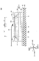
- FIG. 2 is a cross-sectional view showing the semiconductor device according to the first embodiment.
- FIG. 3 is a top view showing the semiconductor device according to the second embodiment.
- FIG. 4 is a top view showing the semiconductor device according to the third embodiment.
- FIG. 5 is a cross-sectional view showing a semiconductor device according to the third embodiment.
- FIG. 6 is a top view showing the semiconductor device according to the fourth embodiment.
- FIG. 7 is a cross-sectional view showing a semiconductor device according to a fourth embodiment.
- FIG. 8 is a top view showing the semiconductor device according to the fifth embodiment.
- FIG. 9 is a top view showing a semiconductor module according to the sixth embodiment.
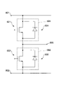
- FIG. 10 is a circuit diagram showing a semiconductor module according to the sixth embodiment.
- a conventional semiconductor device may not have sufficient avalanche resistance after mounting.
- An object of the present disclosure is to provide a semiconductor device capable of improving the avalanche resistance after mounting.
- a semiconductor device includes a silicon carbide substrate having a first main surface, an electrode on the first main surface, and a connection member connected to the electrode,
- the first main surface is inclined from (0001), and the planar shape of the electrode when viewed in plan from a direction perpendicular to the first main surface is parallel to [1-100] of the silicon carbide substrate.
- a rectangle or rounded rectangle having one side and a second side, wherein the first side is on the [-1-120] side with respect to the second side, and the second side is the first side is on the [11-20] side with respect to, the shortest distance between the first side and the contact area where the connection member contacts the electrode is defined as a first distance, and the second side and the contact area The first distance is greater than the second distance when the shortest distance between is the second distance.
- Silicon carbide has anisotropy in dielectric breakdown strength. For example, if the strength of the electric field is the same, when comparing the case where the electric field is applied to [11-20] and the case where the electric field is applied to [0001], dielectric breakdown is more likely to occur in the former.
- the first side is on the [-1-120] side with respect to the second side
- the second side is on the [11-20] side with respect to the first side.
- the first distance is greater than the second distance.
- an avalanche current flows through the electrode to the connection member, but the electrical resistance of the electrode reduces the current flowing through the connection member. Therefore, the avalanche resistance can be improved.
- a semiconductor device includes a silicon carbide substrate having a first main surface, an electrode on the first main surface, and a connecting member connected to the electrode.
- the first main surface is inclined from (000-1), and the planar shape of the electrode when viewed from the direction perpendicular to the first main surface is [1-100] of the silicon carbide substrate.
- the shortest distance between the first side and the contact area where the connecting member contacts the electrode, which is located on the [11-20] side with respect to the first side, is defined as a first distance, and the second side and The first distance is greater than the second distance, where the shortest distance to the contact area is the second distance.
- a semiconductor device includes a silicon carbide substrate having a first main surface, an electrode on the first main surface, and a connection member connected to the electrode. and the first main surface is inclined from ⁇ 0001 ⁇ , and the planar shape of the electrode when viewed in plan from a direction perpendicular to the first main surface is parallel to [1-100] of the silicon carbide substrate.
- the silicon carbide substrate is a rectangle or a rectangle with rounded corners having first and second sides, and the silicon carbide substrate includes a first region overlapping the first sides when viewed from above in a direction perpendicular to the first main surface.
- the first distance is greater than the second distance, where the shortest distance between the member and the contact area is a first distance, and the shortest distance between the second side and the contact area is a second distance.
- the dielectric breakdown strength of the first region is lower than that of the second region, avalanche breakdown is more likely to occur in the first region than in the second region.
- the first distance is greater than the second distance. Therefore, when an avalanche breakdown occurs in the first region in plan view, the avalanche current flows through the electrode to the connection member, but the electrical resistance of the electrode reduces the current flowing through the connection member. Therefore, the avalanche resistance can be improved.
- connection members may be arranged in [1-100] and connected to the electrodes. In this case, it is easy to ensure a large first distance.
- connection members may be arranged in line in [11-20] and connected to the electrodes. Even when a plurality of connecting members are arranged in [11-20], if the first distance is longer than the second distance, the avalanche resistance can be improved.
- connection member may be a bonding wire and may be stitch-connected to the electrode at a plurality of points. In this case, the connection reliability of the connection member can be improved.
- connection member may be a metal plate. In this case, it is easy to reduce the electric resistance of the connection member and reduce the power loss.
- the first main surface may be a surface inclined from ⁇ 0001 ⁇ in the ⁇ 11-20> direction at an off angle of 0.1 degree or more and 8 degrees or less. . In this case, it is easy to obtain good crystals.
- a mark may be provided on the silicon carbide substrate or the electrode to specify the crystal orientation of the silicon carbide substrate. In this case, when mounting the silicon carbide substrate, it is possible to easily recognize in which direction the silicon carbide substrate should be arranged.
- the difference between the first distance and the second distance may be 500 ⁇ m or more. In this case, better avalanche resistance is obtained.
- the combination of the silicon carbide substrate and the electrode may constitute a transistor or a diode.
- the avalanche resistance of the transistor or diode can be improved.
- connection member may be electrically connected to an external terminal.
- the resistance to avalanche breakdown due to the application of voltage from the external terminal can be improved.
- the combination of the silicon carbide substrate and the electrode constitutes a transistor
- the carbonization A combination of the silicon substrate and the electrode may constitute a diode, and the transistor and the diode may be connected in parallel with each other.
- the diode can act as the freewheeling diode of the transistor. Then, the avalanche resistance can be improved in each of the transistor and the diode.
- the combination of the silicon carbide substrate and the electrode constitutes a first transistor
- a combination of the silicon carbide substrate and the electrode may constitute a second transistor
- the first transistor and the second transistor may be connected in series with each other.
- a power module can be configured that includes the first transistor and the second transistor.
- a first transistor can be included in the upper arm and a second transistor can be included in the lower arm. Then, the avalanche resistance can be improved in each of the first transistor and the second transistor.
- a plane including the X1-X2 direction and the Y1-Y2 direction is the XY plane
- a plane including the Y1-Y2 direction and the Z1-Z2 direction is the YZ plane
- a plane including the Z1-Z2 direction and the X1-X2 direction is the ZX plane.
- the Z1 direction is defined as the upward direction
- the Z2 direction is defined as the downward direction.
- planar viewing means viewing an object from the Z1 side.
- FIG. 1 is a top view showing the semiconductor device according to the first embodiment.
- FIG. 2 is a cross-sectional view showing the semiconductor device according to the first embodiment.
- FIG. 2 corresponds to a cross-sectional view taken along line II-II in FIG.
- the semiconductor device 100 has a silicon carbide substrate 10, an anode electrode 20, a cathode electrode 30, and bonding wires 40.
- Silicon carbide substrate 10 includes silicon carbide single crystal substrate 101 and silicon carbide epitaxial layer 102 on silicon carbide single crystal substrate 101 .
- Silicon carbide substrate 10 has a first main surface 10A and a second main surface 10B opposite to first main surface 10A.
- Silicon carbide epitaxial layer 102 forms first main surface 10A
- silicon carbide single-crystal substrate 101 forms second main surface 10B.
- Silicon carbide substrate 10 has a rectangular parallelepiped shape, for example.
- the first main surface 10A is a surface perpendicular to the Z1-Z2 direction. [1-100] is the direction parallel to the X1-X2 direction.
- Silicon carbide single-crystal substrate 101 and silicon carbide epitaxial layer 102 are made of hexagonal silicon carbide of polytype 4H, for example. Silicon carbide epitaxial layer 102 on silicon carbide single-crystal substrate 101 has n-type including n-type impurities such as nitrogen (N).
- the first main surface 10A is a surface in which (0001) is inclined in the off direction.
- the off direction is [11-20].
- the first main surface 10A is a surface in which (0001) is inclined by an off angle of 8° or less in the off direction ([11-20]).
- the off angle may be, for example, 0.8° or more, or may be 2° or more.
- the off angle may be 6° or less, or may be 4° or less.
- [11-20] is the direction within (0001). However, since the first main surface 10A is a surface in which (0001) is inclined in the off direction, [11-20] is not an orientation within the first main surface 10A.
- the Y1 direction corresponds to the direction of [-1-120] projected onto the first main surface 10A, and the Y2 direction corresponds to the direction of [11-20] projected onto the first main surface 10A.
- a first P-type region 16 and a second P-type region 17 are formed on the first main surface 10A.
- the second P-type region 17 surrounds the first P-type region 16 in plan view.
- the second P-type region 17 functions as a breakdown voltage maintaining region.
- the anode electrode 20 is provided on the first main surface 10A.
- the anode electrode 20 contains, for example, aluminum (Al).
- Anode electrode 20 is provided, for example, on a portion of first main surface 10A, and the edge of anode electrode 20 may be inside the edge of silicon carbide substrate 10 in plan view.
- the planar shape of the anode electrode 20 when viewed from the direction perpendicular to the first main surface 10A is, for example, a first side 21 and a second side 22 parallel to [1-100] of the silicon carbide substrate 10. It is a rounded rectangle.
- the first side 21 and the second side 22 are parallel to the X1-X2 direction.
- the first side 21 is on the Y1 direction side with respect to the second side 22 .
- first side 21 is on the [-1-120] side with respect to the second side 22 .
- second side 22 is on the Y2 direction side with respect to the first side 21 . That is, the second side 22 is on the [11-20] side with respect to the first side 21 .
- the planar shape of anode electrode 20 when viewed from the direction perpendicular to first main surface 10A is a rectangle having first side 21 and second side 22 parallel to [1-100] of silicon carbide substrate 10. There may be.
- a mark 19 specifying the crystal orientation of silicon carbide substrate 10 may be provided on a portion of first main surface 10A exposed from anode electrode 20 .
- Labels 19 may directly indicate crystal orientation. For example, which direction [11-20] faces may be displayed using Miller's index or a figure such as a triangle. Further, the crystal orientation of silicon carbide substrate 10 may be indicated indirectly by the orientation of the product number or the like.
- the cathode electrode 30 is provided on the second main surface 10B.
- the cathode electrode 30 contains nickel (Ni), nickel silicide (NiSi), or titanium aluminum silicide (TiAlSi), for example.
- the cathode electrode 30 may be provided, for example, over the entire surface of the second main surface 10B.
- the cathode electrode 30 is bonded onto, for example, a conductive layer 91 formed on the main surface of an insulating substrate 90 using a bonding material (not shown) such as solder.
- the conductive layer 91 is electrically connected to an external terminal such as a power supply terminal or an output terminal. In FIG. 1, the insulating substrate 90 and the conductive layer 91 are omitted.
- a plurality of, for example four, bonding wires 40 are connected to the anode electrode 20 .
- a plurality of bonding wires 40 contact the anode electrode 20 at contact regions 50 of the anode electrode 20 .
- the contact area 50 has, for example, a rectangular planar shape having two sides parallel to the X1-X2 direction and two sides parallel to the Y1-Y2 direction. In plan view, the dimension of the contact region 50 in the Y1-Y2 direction is smaller than the dimension in the X1-X2 direction, and the plurality of bonding wires 40 are aligned in the X1-X2 direction and are in contact with the anode electrode 20 .
- a plurality of bonding wires 40 are arranged in [1-100] and connected to the anode electrode 20 .
- the bonding wire 40 is electrically connected to an external terminal such as a power supply terminal or an output terminal.
- the bonding wire 40 is an example of a connection member.
- the number of bonding wires 40 is not limited. The number of bonding wires 40 may be one.
- the contact region 50 is a region in which the bonding wire 40 contacts the anode electrode 20 and is a minimum rectangular region including two sides parallel to the first side 21 and the second side 22 .
- the first distance L1 is the 2 greater than the distance L2.
- the first main surface 10A is a surface in which (0001) is inclined in the off direction.
- the off direction is [11-20]. Therefore, as shown in FIG. 2, [11-20] is non-parallel to the first major surface 10A.
- Silicon carbide has anisotropic dielectric breakdown strength. For example, if the strength of the electric field is the same, when comparing the case where the electric field is applied to [11-20] of silicon carbide and the case where the electric field is applied to [0001] of silicon carbide, in the former, Dielectric breakdown strength is low and dielectric breakdown is likely to occur. Therefore, the dielectric breakdown strength of the first region 11 overlapping the first side 21 of the anode electrode 20 in plan view is lower than the dielectric breakdown strength of the second region 12 overlapping the second side 22 of the anode electrode 20 in plan view.
- an electric field of equipotential surfaces having a distribution as indicated by the dashed line in FIG. 2 is generated.
- the strength of the electric field E1 in the first region 11 is the same as the strength of the electric field E2 in the second region 12, but the proportion of the [11-20] component in the electric field E1 is greater than the electric field E2, and the [0001] component is smaller in electric field E1 than in electric field E2. Therefore, avalanche breakdown is more likely to occur in the first region 11 than in the second region 12 .
- the first distance L1 is greater than the second distance L2. Therefore, when avalanche breakdown occurs in the first region 11 , an avalanche current flows through the bonding wire 40 through the anode electrode 20 , but the electrical resistance of the anode electrode 20 reduces the current flowing through the bonding wire 40 . Therefore, the avalanche resistance can be improved.
- the bonding wires 40 are connected to the anode electrode 20 along [1-100], it is easy to ensure a large first distance L1, and it is easy to improve the avalanche resistance.
- the mark 19 it is possible to easily recognize in which direction the silicon carbide substrate 10 should be arranged when the silicon carbide substrate 10 is mounted.
- the label 19 may be provided on the anode electrode 20 instead of the silicon carbide substrate 10 .
- FIG. 3 is a top view showing the semiconductor device according to the second embodiment.
- each bonding wire 40 is stitch-connected to the anode electrode 20 at a plurality of locations, for example, two locations. Also in the second embodiment, each bonding wire 40 is in contact with the anode electrode 20 at the contact area 50 of the anode electrode 20 and is connected to the anode electrode 20 along [1-100]. Also in the second embodiment, the first distance L1 is greater than the second distance L2.
- each bonding wire 40 is connected to the anode electrode 20 at a plurality of points, connection reliability can be improved.
- FIG. 4 is a top view showing the semiconductor device according to the third embodiment.
- FIG. 5 is a cross-sectional view showing a semiconductor device according to the third embodiment.
- FIG. 5 corresponds to a cross-sectional view taken along line VV in FIG.
- a semiconductor device 300 has a silicon carbide substrate 10, an anode electrode 20, a cathode electrode 30, and a metal plate 60. That is, the metal plate 60 is provided instead of the bonding wires 40 .
- the metal plate 60 is, for example, a copper (Cu) plate.
- the metal plate 60 has a surface 61 that contacts the contact area 50 and contacts the anode electrode 20 at the contact area 50 of the anode electrode 20 .
- the metal plate 60 is electrically connected to an external terminal such as a power terminal or an output terminal.
- Metal plate 60 is an example of a connecting member.
- the first distance L1 is longer than the second distance L2.
- the contact area 50 is an area in which the metal plate 60 contacts the anode electrode 20 and is a minimum rectangular area including two sides parallel to the first side 21 and the second side 22 .
- the same effect as the first embodiment can be obtained by the third embodiment. Also, since the metal plate 60 is provided, electrical resistance can be reduced, and power loss can be reduced.
- FIG. 6 is a top view showing the semiconductor device according to the fourth embodiment.
- FIG. 7 is a cross-sectional view showing a semiconductor device according to a fourth embodiment.
- FIG. 7 corresponds to a cross-sectional view taken along line VII-VII in FIG.
- the dimension in the Y1-Y2 direction of the contact region 50 is larger than the dimension in the X1-X2 direction in plan view, and the plurality of bonding wires 40 are in contact with the anode electrode 20 so as to be aligned in the Y1-Y2 direction. That is, a plurality of bonding wires 40 are connected to the anode electrode 20 in a line [11-20]. Also in the fourth embodiment, the first distance L1 is longer than the second distance L2.
- the difference between the first distance L1 and the second distance L2 is, for example, 200 ⁇ m or more.
- the difference between the first distance L1 and the second distance L2 is preferably 500 ⁇ m or more, more preferably 600 ⁇ m or more, and even more preferably 700 ⁇ m or more. This is because a better avalanche resistance can be obtained.
- FIG. 8 is a top view showing the semiconductor device according to the fifth embodiment.
- a semiconductor device 500 includes a silicon carbide substrate 10, a source electrode 70, a gate electrode 80, a drain electrode (not shown), bonding wires 41, bonding wires 42.
- the source electrode 70 is provided on the first main surface 10A.
- the source electrode 70 contains aluminum (Al), for example.
- Source electrode 70 is provided, for example, on a portion of first main surface 10A, and the edge of source electrode 70 may be inside the edge of silicon carbide substrate 10 in plan view.
- the planar shape of the source electrode 70 when viewed from the direction perpendicular to the first main surface 10A is, for example, a first side 71 and a second side 72 parallel to [1-100] of the silicon carbide substrate 10. It is a rounded rectangle.
- the first side 71 and the second side 72 are parallel to the X1-X2 direction.
- the first side 71 is on the Y1 direction side with respect to the second side 72 .
- first side 71 is on the [-1-120] side with respect to the second side 72 .
- second side 72 is on the Y2 direction side with respect to the first side 71 . That is, the second side 72 is on the [11-20] side with respect to the first side 71 .
- the planar shape of source electrode 70 when viewed from the direction perpendicular to first main surface 10A is a rectangle having first side 71 and second side 72 parallel to [1-100] of silicon carbide substrate 10. There may be.
- a recess 73 recessed toward the second side 72 is formed in the first side 71 of the source electrode 70 , and the gate electrode 80 is formed inside the recess 73 .
- a drain electrode is provided on the second main surface 10B.
- the drain electrode may be provided, for example, over the entire surface of the second main surface 10B.
- a plurality of, for example, four bonding wires 41 are connected to the source electrode 70 .
- a plurality of bonding wires 41 contact the source electrode 70 at the contact region 50 of the source electrode 70 .
- the contact area 50 has, for example, a rectangular planar shape having two sides parallel to the X1-X2 direction and two sides parallel to the Y1-Y2 direction. In plan view, the dimension in the Y1-Y2 direction of the contact region 50 is smaller than the dimension in the X1-X2 direction, and the plurality of bonding wires 41 are aligned in the X1-X2 direction and are in contact with the source electrode 70 . That is, a plurality of bonding wires 41 are arranged in [1-100] and connected to the source electrode 70 .
- the bonding wire 41 is electrically connected to an external terminal such as a power supply terminal or an output terminal.
- the bonding wire 41 is an example of a connecting member.
- the number of bonding wires 41 is not limited. The number of bonding wires 41 may be one. Also in the fifth embodiment, the first distance L1 is greater than the second distance L2.
- the bonding wire 42 is connected to the gate electrode 80 .
- Label 19 may be provided on silicon carbide substrate 10 or source electrode 70 .
- the bonding wires 41 may be stitch-connected to the source electrode 70 at a plurality of locations.
- metal plates may be used in place of the bonding wires 41 as in the third embodiment.
- the dimension of the contact region 50 in the Y1-Y2 direction is larger than the dimension in the X1-X2 direction, and the plurality of bonding wires 41 are arranged in the Y1-Y2 direction. They may be in contact with the source electrode 70 so as to line up.
- semiconductor devices are not limited to PN junction diodes and MOSFETs.
- the semiconductor device may be a Schottky barrier diode or an insulated gate bipolar transistor (IGBT).
- IGBT insulated gate bipolar transistor
- the first main surface of the silicon carbide substrate may be a surface inclined from (000-1). Also in this case, the first side is on the [-1-120] side with respect to the second side, the second side is on the [11-20] side with respect to the first side, and the first distance is the second distance greater than
- FIG. 9 is a top view showing a semiconductor module according to the sixth embodiment.
- FIG. 10 is a circuit diagram showing a semiconductor module according to the sixth embodiment.
- a semiconductor module 600 includes a P terminal 601, an N terminal 602, an O terminal 603, a first conductive pattern 611, a second conductive pattern 612, and a third conductive pattern. and a pattern 613 .
- the semiconductor module 600 further has a first transistor 621 , a second transistor 622 , a first diode 631 and a second diode 632 .
- the P terminal 601 is electrically connected to the first conductive pattern 611
- the O terminal 603 is electrically connected to the second conductive pattern 612
- the N terminal 602 is electrically connected to the third conductive pattern 613 .
- a first transistor 621 and a first diode 631 are provided on the first conductive pattern 611 .
- a drain electrode of the first transistor 621 and a cathode electrode of the first diode 631 are joined to the first conductive pattern 611 using a joining material (not shown) such as solder.
- a source electrode 641 of the first transistor 621 is connected to the second conductive pattern 612 by a plurality of bonding wires 661 .
- Anode electrode 651 of first diode 631 is connected to source electrode 641 of first transistor 621 by a plurality of bonding wires 671 .
- the first transistor 621 has a contact area similar to the contact area 50 of the fifth embodiment, and the bonding wire 661 contacts the source electrode 641 of the first transistor 621 at this contact area.
- the first diode 631 has a contact area similar to the contact area 50 of the first to fourth embodiments, and the bonding wire 671 contacts the anode electrode 651 of the first diode 631 at this contact area.
- a second transistor 622 and a second diode 632 are provided on the second conductive pattern 612 .
- a drain electrode of the second transistor 622 and a cathode electrode of the second diode 632 are bonded to the second conductive pattern 612 using a bonding material (not shown) such as solder.
- a source electrode 642 of the second transistor 622 is connected to the third conductive pattern 613 by a plurality of bonding wires 662 .
- Anode electrode 652 of second diode 632 is connected to source electrode 642 of second transistor 622 by a plurality of bonding wires 672 .
- the second transistor 622 has a contact area similar to the contact area 50 of the fifth embodiment, and the bonding wire 662 contacts the source electrode 642 of the second transistor 622 at this contact area.
- the second diode 632 has a contact area similar to the contact area 50 of the first to fourth embodiments, and the bonding wire 672 contacts the anode electrode 652 of the second diode 632 at this contact area.
- a first transistor 621 and a second transistor 622 are connected in series between a P terminal 601 and an N terminal 602, and an O terminal 603 is connected between the first transistor 621 and the second transistor. 2 transistor 622 .
- a first diode 631 is connected in parallel with the first transistor 621 and a second diode 632 is connected in parallel with the second transistor 622 .
- An upper arm 681 including a first transistor 621 and a first diode 631 is configured, and a lower arm 682 including a second transistor 622 and a second diode 632 is configured.
- the first transistor 621, the second transistor 622, the first diode 631 and the second diode 632 have excellent avalanche resistance.
- the bonding wire is in contact with the same contact region as the contact region 50, but it is not limited to this. .
Landscapes
- Electrodes Of Semiconductors (AREA)
Abstract
半導体装置は、第1主面を備えた炭化珪素基板と、前記第1主面上の電極と、前記電極に接続された接続部材と、を有し、前記第1主面は、(0001)から傾斜し、前記第1主面に垂直な方向から平面視したときの前記電極の平面形状は、前記炭化珪素基板の[1-100]に平行な第1辺及び第2辺を備えた矩形又は角丸矩形であり、前記第1辺は、前記第2辺に対して[-1-120]側にあり、前記第2辺は、前記第1辺に対して[11-20]側にあり、前記第1辺と、前記電極に前記接続部材が接触する接触領域との間の最短距離を第1距離とし、前記第2辺と前記接触領域との間の最短距離を第2距離としたとき、第1距離が第2距離より大きい。
Description
本開示は、半導体装置に関する。
本出願は、2021年3月31日出願の日本出願第2021-061026号に基づく優先権を主張し、前記日本出願に記載された全ての記載内容を援用するものである。
複数の半導体装置をワイヤボンディングにより接続した半導体モジュールが提案されている(例えば特許文献1)。また、終端構造等の配置により耐圧の向上を図った半導体装置が提案されている(例えば特許文献2及び3)。
本開示の半導体装置は、第1主面を備えた炭化珪素基板と、前記第1主面上の電極と、前記電極に接続された接続部材と、を有し、前記第1主面は、(0001)から傾斜し、前記第1主面に垂直な方向から平面視したときの前記電極の平面形状は、前記炭化珪素基板の[1-100]に平行な第1辺及び第2辺を備えた矩形又は角丸矩形であり、前記第1辺は、前記第2辺に対して[-1-120]側にあり、前記第2辺は、前記第1辺に対して[11-20]側にあり、前記第1辺と、前記電極に前記接続部材が接触する接触領域との間の最短距離を第1距離とし、前記第2辺と前記接触領域との間の最短距離を第2距離としたとき、第1距離が第2距離より大きい。
[本開示が解決しようとする課題]
従来の半導体装置では、実装後に十分なアバランシェ耐量が得られないことがある。
従来の半導体装置では、実装後に十分なアバランシェ耐量が得られないことがある。
本開示は、実装後のアバランシェ耐量を向上できる半導体装置を提供することを目的とする。
[本開示の効果]
本開示によれば、実装後のアバランシェ耐量を向上できる。
本開示によれば、実装後のアバランシェ耐量を向上できる。
実施するための形態について、以下に説明する。
[本開示の実施形態の説明]
最初に本開示の実施態様を列記して説明する。以下の説明では、同一または対応する要素には同一の符号を付し、それらについて同じ説明は繰り返さない。本明細書中の結晶学的記載においては、個別方位を[]、集合方位を<>、個別面を()、集合面を{}でそれぞれ示している。また結晶学上の指数が負であることは、通常、"-"(バー)を数字の上に付すことによって表現されるが、本明細書中では数字の前に負の符号を付している。
最初に本開示の実施態様を列記して説明する。以下の説明では、同一または対応する要素には同一の符号を付し、それらについて同じ説明は繰り返さない。本明細書中の結晶学的記載においては、個別方位を[]、集合方位を<>、個別面を()、集合面を{}でそれぞれ示している。また結晶学上の指数が負であることは、通常、"-"(バー)を数字の上に付すことによって表現されるが、本明細書中では数字の前に負の符号を付している。
〔1〕 本開示の一態様に係る半導体装置は、第1主面を備えた炭化珪素基板と、前記第1主面上の電極と、前記電極に接続された接続部材と、を有し、前記第1主面は、(0001)から傾斜し、前記第1主面に垂直な方向から平面視したときの前記電極の平面形状は、前記炭化珪素基板の[1-100]に平行な第1辺及び第2辺を備えた矩形又は角丸矩形であり、前記第1辺は、前記第2辺に対して[-1-120]側にあり、前記第2辺は、前記第1辺に対して[11-20]側にあり、前記第1辺と、前記電極に前記接続部材が接触する接触領域との間の最短距離を第1距離とし、前記第2辺と前記接触領域との間の最短距離を第2距離としたとき、第1距離が第2距離より大きい。
炭化珪素は絶縁破壊強度に異方性を有する。例えば、電界の強さが同等であれば、[11-20]に電界が印加された場合と、[0001]に電界が印加された場合とを比較すると、前者において絶縁破壊が生じやすい。本半導体装置では、第1辺が第2辺に対して[-1-120]側にあり、第2辺が第1辺に対して[11-20]側にあるため、アバランシェ降伏は平面視で第1辺と重なる領域において、平面視で第2辺と重なる領域よりも生じやすい。また、本半導体装置では、第1距離が第2距離より大きい。このため、アバランシェ降伏が平面視で第1辺と重なる領域において生じると、アバランシェ電流が電極を通じて接続部材に流れるものの、電極の電気抵抗により接続部材に流れる電流が低減される。従って、アバランシェ耐量を向上できる。
〔2〕 本開示の他の一態様に係る半導体装置は、第1主面を備えた炭化珪素基板と、前記第1主面上の電極と、前記電極に接続された接続部材と、を有し、前記第1主面は、(000-1)から傾斜し、前記第1主面に垂直な方向から平面視したときの前記電極の平面形状は、前記炭化珪素基板の[1-100]に平行な第1辺及び第2辺を備えた矩形又は角丸矩形であり、前記第1辺は、前記第2辺に対して[-1-120]側にあり、前記第2辺は、前記第1辺に対して[11-20]側にあり、前記第1辺と、前記電極に前記接続部材が接触する接触領域との間の最短距離を第1距離とし、前記第2辺と前記接触領域との間の最短距離を第2距離としたとき、第1距離が第2距離より大きい。
〔1〕に記載の半導体装置と同様に、アバランシェ降伏が平面視で第1辺と重なる領域において生じると、アバランシェ電流が電極を通じて接続部材に流れるものの、電極の電気抵抗により接続部材に流れる電流が低減される。従って、アバランシェ耐量を向上できる。
〔3〕 本開示の他の一態様に係る半導体装置は、第1主面を備えた炭化珪素基板と、前記第1主面上の電極と、前記電極に接続された接続部材と、を有し、前記第1主面は、{0001}から傾斜し、前記第1主面に垂直な方向から平面視したときの前記電極の平面形状は、前記炭化珪素基板の[1-100]に平行な第1辺及び第2辺を備えた矩形又は角丸矩形であり、前記第1主面に垂直な方向から平面視したときに、前記炭化珪素基板は、前記第1辺と重なる第1領域と、前記第2辺と重なる第2領域と、を有し、前記第1領域の絶縁破壊強度は、前記第2領域の絶縁破壊強度よりも低く、前記第1辺と、前記電極に前記接続部材が接触する接触領域との間の最短距離を第1距離とし、前記第2辺と前記接触領域との間の最短距離を第2距離としたとき、第1距離が第2距離より大きい。
本半導体装置では、第1領域の絶縁破壊強度が第2領域の絶縁破壊強度よりも低いため、アバランシェ降伏は第1領域において、第2領域よりも生じやすい。また、本半導体装置では、第1距離が第2距離より大きい。このため、アバランシェ降伏が平面視で第1領域において生じると、アバランシェ電流が電極を通じて接続部材に流れるものの、電極の電気抵抗により接続部材に流れる電流が低減される。従って、アバランシェ耐量を向上できる。
〔4〕 〔1〕~〔3〕において、複数の前記接続部材が[1-100]に並んで前記電極に接続されていてもよい。この場合、第1距離を大きく確保しやすい。
〔5〕 〔1〕~〔3〕において、複数の前記接続部材が[11-20]に並んで前記電極に接続されていてもよい。複数の接続部材が[11-20]に並んでいる場合でも、第1距離が第2距離より大きければ、アバランシェ耐量を向上できる。
〔6〕 〔1〕~〔5〕において、前記接続部材はボンディングワイヤであり、前記電極に複数個所でスティッチ接続されていてもよい。この場合、接続部材の接続信頼性を向上できる。
〔7〕 〔1〕~〔3〕において、前記接続部材は金属板であってもよい。この場合、接続部材の電気抵抗を低減し、電力損失を低減しやすい。
〔8〕 〔1〕~〔7〕において、前記第1主面は、{0001}から<11-20>方向に0.1度以上8度以下のオフ角度で傾斜した面であってもよい。この場合、良好な結晶を得やすい。
〔9〕 〔1〕~〔8〕において、前記炭化珪素基板又は前記電極に設けられ、前記炭化珪素基板の結晶方位を特定する標識を有してもよい。この場合、炭化珪素基板の実装の際に、どの向きで炭化珪素基板を配置すべきか認識しやすくできる。
〔10〕 〔1〕~〔9〕において、第1距離と第2距離との差は、500μm以上であってもよい。この場合、より優れたアバランシェ耐量が得られる。
〔11〕 〔1〕~〔10〕において、前記炭化珪素基板と前記電極との組み合わせがトランジスタ又はダイオードを構してもよい。この場合、トランジスタ又はダイオードのアバランシェ耐量を向上できる。
〔12〕 〔1〕~〔11〕において、前記接続部材は電気的に外部端子に接続されてもよい。この場合、外部端子からの電圧の印加に伴うアバランシェ降伏に対する耐量を向上できる。
〔13〕 〔1〕~〔12〕において、前記炭化珪素基板と、前記電極と、前記接続部材との組み合わせを複数有してもよい。この場合、複数の組み合わせにおいてアバランシェ耐量を向上できる。
〔14〕 〔13〕において、複数の前記組み合わせに含まれる第1組み合わせにおいて、前記炭化珪素基板と前記電極との組み合わせがトランジスタを構成し、複数の前記組み合わせに含まれる第2組み合わせにおいて、前記炭化珪素基板と前記電極との組み合わせがダイオードを構成し、前記トランジスタと前記ダイオードとが互いに並列に接続されていてもよい。この場合、ダイオードがトランジスタの還流ダイオードとして機能し得る。そして、トランジスタ及びダイオードの各々においてアバランシェ耐量を向上できる。
〔15〕 〔13〕において、複数の前記組み合わせに含まれる第1組み合わせにおいて、前記炭化珪素基板と前記電極との組み合わせが第1トランジスタを構成し、複数の前記組み合わせに含まれる第2組み合わせにおいて、前記炭化珪素基板と前記電極との組み合わせが第2トランジスタを構成し、前記第1トランジスタと前記第2トランジスタとが互いに直列に接続されていてもよい。この場合、第1トランジスタ及び第2トランジスタを含むパワーモジュールを構成できる。例えば、第1トランジスタを上アームに含ませ、第2トランジスタを下アームに含ませられる。そして、第1トランジスタ及び第2トランジスタの各々においてアバランシェ耐量を向上できる。
[本開示の実施形態の詳細]
以下、本開示の実施形態について詳細に説明するが、本実施形態はこれらに限定されるものではない。なお、本明細書及び図面において、実質的に同一の機能構成を有する構成要素については、同一の符号を付することにより重複した説明を省くことがある。本明細書及び図面において、X1-X2方向、Y1-Y2方向、Z1-Z2方向を相互に直交する方向とする。X1-X2方向及びY1-Y2方向を含む面をXY面とし、Y1-Y2方向及びZ1-Z2方向を含む面をYZ面とし、Z1-Z2方向及びX1-X2方向を含む面をZX面とする。便宜上、Z1方向を上方向、Z2方向を下方向とする。また、本開示において平面視とは、Z1側から対象物を視ることをいう。
以下、本開示の実施形態について詳細に説明するが、本実施形態はこれらに限定されるものではない。なお、本明細書及び図面において、実質的に同一の機能構成を有する構成要素については、同一の符号を付することにより重複した説明を省くことがある。本明細書及び図面において、X1-X2方向、Y1-Y2方向、Z1-Z2方向を相互に直交する方向とする。X1-X2方向及びY1-Y2方向を含む面をXY面とし、Y1-Y2方向及びZ1-Z2方向を含む面をYZ面とし、Z1-Z2方向及びX1-X2方向を含む面をZX面とする。便宜上、Z1方向を上方向、Z2方向を下方向とする。また、本開示において平面視とは、Z1側から対象物を視ることをいう。
(第1実施形態)
まず、第1実施形態について説明する。第1実施形態は、PN接合ダイオードに関する。図1は、第1実施形態に係る半導体装置を示す上面図である。図2は、第1実施形態に係る半導体装置を示す断面図である。図2は、図1中のII-II線に沿った断面図に相当する。
まず、第1実施形態について説明する。第1実施形態は、PN接合ダイオードに関する。図1は、第1実施形態に係る半導体装置を示す上面図である。図2は、第1実施形態に係る半導体装置を示す断面図である。図2は、図1中のII-II線に沿った断面図に相当する。
図1及び図2に示すように、第1実施形態に係る半導体装置100は、炭化珪素基板10と、アノード電極20と、カソード電極30と、ボンディングワイヤ40とを有する。
炭化珪素基板10は、炭化珪素単結晶基板101と、炭化珪素単結晶基板101の上の炭化珪素エピタキシャル層102とを含む。炭化珪素基板10は、第1主面10Aと、第1主面10Aとは反対側の第2主面10Bとを有する。炭化珪素エピタキシャル層102が第1主面10Aを構成し、炭化珪素単結晶基板101が第2主面10Bを構成する。炭化珪素基板10の形状は、例えば直方体状である。第1主面10AはZ1-Z2方向に垂直な面である。[1-100]はX1-X2方向に平行な方向である。炭化珪素単結晶基板101及び炭化珪素エピタキシャル層102は、例えばポリタイプ4Hの六方晶炭化珪素から構成されている。炭化珪素単結晶基板101の上の炭化珪素エピタキシャル層102は、例えば窒素(N)等のn型不純物を含みn型を有する。
第1主面10Aは、(0001)がオフ方向に傾斜した面である。例えば、オフ方向は[11-20]である。例えば、第1主面10Aは(0001)がオフ方向([11-20])に8°以下のオフ角だけ傾斜した面である。オフ角は、例えば0.8°以上であってもよいし、2°以上であってもよい。オフ角は、6°以下であってもよいし、4°以下であってもよい。
[11-20]は(0001)内の方位である。しかし、第1主面10Aが(0001)がオフ方向に傾斜した面であるため、[11-20]は第1主面10A内の方位ではない。Y1方向は[-1-120]を第1主面10Aに投影した方位に相当し、Y2方向は[11-20]を第1主面10Aに投影した方位に相当する。
第1主面10Aに第1P型領域16と第2P型領域17とが形成されている。平面視で第2P型領域17は第1P型領域16を囲んでいる。第2P型領域17は耐圧維持領域として機能する。
アノード電極20は第1主面10Aに設けられている。アノード電極20は、例えばアルミニウム(Al)を含む。アノード電極20は、例えば、第1主面10Aの一部に設けられており、平面視で、アノード電極20の縁は、炭化珪素基板10の縁の内側にあってもよい。第1主面10Aに垂直な方向から平面視したときのアノード電極20の平面形状は、例えば、炭化珪素基板10の[1-100]に平行な第1辺21及び第2辺22を備えた角丸矩形である。第1辺21及び第2辺22はX1-X2方向に平行である。第1辺21は第2辺22に対してY1方向側にある。つまり、第1辺21は第2辺22に対して[-1-120]側にある。また、第2辺22は第1辺21に対してY2方向側にある。つまり、第2辺22は、第1辺21に対して[11-20]側にある。第1主面10Aに垂直な方向から平面視したときのアノード電極20の平面形状が、炭化珪素基板10の[1-100]に平行な第1辺21及び第2辺22を備えた矩形であってもよい。
第1主面10Aのアノード電極20から露出した部分に、炭化珪素基板10の結晶方位を特定する標識19が設けられていてもよい。標識19は直接的に結晶方位を表示してもよい。例えば[11-20]がどの方向を向いているのかをミラー指数又は三角形等の図形を用いて表示してもよい。また、製品番号の向き等により炭化珪素基板10の結晶方位を間接的に表示してもよい。
カソード電極30は第2主面10Bに設けられている。カソード電極30は、例えばニッケル(Ni)、ニッケルシリサイド(NiSi)又はチタンアルミニウムシリサイド(TiAlSi)を含む。カソード電極30は、例えば、第2主面10Bの全面に設けられていてもよい。カソード電極30は、例えば絶縁基板90の主面に形成された導電層91の上に、はんだ等の接合材(図示せず)を用いて接合される。導電層91は、例えば電源端子又は出力端子等の外部端子に電気的に接続される。図1では、絶縁基板90及び導電層91を省略している。
複数、例えば4本のボンディングワイヤ40がアノード電極20に接続されている。複数のボンディングワイヤ40は、アノード電極20の接触領域50にてアノード電極20に接触している。接触領域50は、例えば、X1-X2方向に平行な2辺と、Y1-Y2方向に平行な2辺とを有する矩形状の平面形状を備える。平面視で、接触領域50のY1-Y2方向の寸法はX1-X2方向の寸法よりも小さく、複数のボンディングワイヤ40はX1-X2方向に並ぶようにしてアノード電極20に接触している。つまり、複数のボンディングワイヤ40が[1-100]に並んでアノード電極20に接続されている。ボンディングワイヤ40は、例えば電源端子又は出力端子等の外部端子に電気的に接続される。ボンディングワイヤ40は接続部材の一例である。ボンディングワイヤ40の数は限定されない。ボンディングワイヤ40が1本であってもよい。接触領域50は、その内側でボンディングワイヤ40がアノード電極20に接触する領域であって、第1辺21及び第2辺22に平行な2辺を含む最小の矩形の領域である。
第1辺21と接触領域50との間の最短距離を第1距離L1とし、第2辺22と接触領域50との間の最短距離を第2距離L2としたとき、第1距離L1は第2距離L2より大きい。
ここで、第1実施形態の作用効果について説明する。
第1主面10Aは、(0001)がオフ方向に傾斜した面である。例えば、オフ方向は[11-20]である。このため、図2に示すように、[11-20]は第1主面10Aに非平行である。炭化珪素は絶縁破壊強度に異方性を有する。例えば、電界の強さが同等であれば、炭化珪素の[11-20]に電界が印加された場合と、炭化珪素の[0001]に電界が印加された場合とを比較すると、前者において、絶縁破壊強度が小さく絶縁破壊が生じやすい。従って、平面視でアノード電極20の第1辺21と重なる第1領域11の絶縁破壊強度は、平面視でアノード電極20の第2辺22と重なる第2領域12の絶縁破壊強度よりも低い。
また、アノード電極20とカソード電極30との間に電圧が印加されると、図2中に破線で示すような分布の等電位面の電界が発生する。第1領域11における電界E1の強さは第2領域12における電界E2の強さと同等であるが、[11-20]の成分の割合は電界E1において電界E2よりも大きく、[0001]の成分の割合は電界E1において電界E2よりも小さい。このため、アバランシェ降伏は第1領域11において第2領域12よりも生じやすい。
本実施形態では、第1距離L1が第2距離L2より大きい。このため、アバランシェ降伏が第1領域11において生じると、アバランシェ電流がアノード電極20を通じてボンディングワイヤ40に流れるものの、アノード電極20の電気抵抗によりボンディングワイヤ40に流れる電流が低減される。従って、アバランシェ耐量を向上できる。
また、ボンディングワイヤ40が[1-100]に並んでアノード電極20に接続されているため、第1距離L1を大きく確保しやすく、アバランシェ耐量をより向上しやすい。
標識19が設けられている場合、炭化珪素基板10の実装の際に、どの向きで炭化珪素基板10を配置すべきか認識しやすくできる。なお、標識19は炭化珪素基板10ではなくアノード電極20に設けられていてもよい。
(第2実施形態)
次に、第2実施形態について説明する。図3は、第2実施形態に係る半導体装置を示す上面図である。
次に、第2実施形態について説明する。図3は、第2実施形態に係る半導体装置を示す上面図である。
図3に示すように、第2実施形態に係る半導体装置200では、各ボンディングワイヤ40がアノード電極20に複数箇所、例えば2箇所でスティッチ接続されている。第2実施形態においても、各ボンディングワイヤ40が、アノード電極20の接触領域50にてアノード電極20に接触し、[1-100]に並んでアノード電極20に接続されている。また、第2実施形態でも、第1距離L1は第2距離L2より大きい。
他の構成は第1実施形態と同様である。
第2実施形態によっても第1実施形態と同様の効果が得られる。また、各ボンディングワイヤ40が複数箇所でアノード電極20に接続されるため、接続信頼性を向上できる。
(第3実施形態)
次に、第3実施形態について説明する。図4は、第3実施形態に係る半導体装置を示す上面図である。図5は、第3実施形態に係る半導体装置を示す断面図である。図5は、図4中のV-V線に沿った断面図に相当する。
次に、第3実施形態について説明する。図4は、第3実施形態に係る半導体装置を示す上面図である。図5は、第3実施形態に係る半導体装置を示す断面図である。図5は、図4中のV-V線に沿った断面図に相当する。
図4及び図5に示すように、第3実施形態に係る半導体装置300は、炭化珪素基板10と、アノード電極20と、カソード電極30と、金属板60とを有する。つまり、複数のボンディングワイヤ40に代えて金属板60が設けられている。金属板60は、例えば銅(Cu)板である。金属板60は、接触領域50に接触する面61を有し、アノード電極20の接触領域50にてアノード電極20に接触している。金属板60は、例えば電源端子又は出力端子等の外部端子に電気的に接続される。金属板60は接続部材の一例である。また、第3実施形態でも、第1距離L1は第2距離L2より大きい。接触領域50は、その内側で金属板60がアノード電極20に接触する領域であって、第1辺21及び第2辺22に平行な2辺を含む最小の矩形の領域である。
他の構成は第1実施形態と同様である。
第3実施形態によっても第1実施形態と同様の効果が得られる。また、金属板60が設けられているため、電気抵抗を低減し、電力損失を低減できる。
(第4実施形態)
次に、第4実施形態について説明する。図6は、第4実施形態に係る半導体装置を示す上面図である。図7は、第4実施形態に係る半導体装置を示す断面図である。図7は、図6中のVII-VII線に沿った断面図に相当する。
次に、第4実施形態について説明する。図6は、第4実施形態に係る半導体装置を示す上面図である。図7は、第4実施形態に係る半導体装置を示す断面図である。図7は、図6中のVII-VII線に沿った断面図に相当する。
図6及び図7に示すように、第4実施形態に係る半導体装置400では、平面視で、接触領域50のY1-Y2方向の寸法がX1-X2方向の寸法よりも大きく、複数のボンディングワイヤ40はY1-Y2方向に並ぶようにしてアノード電極20に接触している。つまり、複数のボンディングワイヤ40が[11-20]に並んでアノード電極20に接続されている。また、第4実施形態でも、第1距離L1は第2距離L2より大きい。
他の構成は第1実施形態と同様である。
第4実施形態によっても第1実施形態と同様の効果が得られる。
第1距離L1と第2距離L2との差は、例えば200μm以上である。第1距離L1と第2距離L2との差は、好ましくは500μm以上であり、より好ましくは600μm以上であり、更に好ましくは700μm以上である。より優れたアバランシェ耐量が得られるためである。
(第5実施形態)
次に、第5実施形態について説明する。第5実施形態は、MOS型電界効果トランジスタ(field effect transistor:FET)に関する。図8は、第5実施形態に係る半導体装置を示す上面図である。
次に、第5実施形態について説明する。第5実施形態は、MOS型電界効果トランジスタ(field effect transistor:FET)に関する。図8は、第5実施形態に係る半導体装置を示す上面図である。
図8に示すように、第5実施形態に係る半導体装置500は、炭化珪素基板10と、ソース電極70と、ゲート電極80と、ドレイン電極(図示せず)と、ボンディングワイヤ41と、ボンディングワイヤ42とを有する。
ソース電極70は第1主面10Aに設けられている。ソース電極70は、例えばアルミニウム(Al)を含む。ソース電極70は、例えば、第1主面10Aの一部に設けられており、平面視で、ソース電極70の縁は、炭化珪素基板10の縁の内側にあってもよい。第1主面10Aに垂直な方向から平面視したときのソース電極70の平面形状は、例えば、炭化珪素基板10の[1-100]に平行な第1辺71及び第2辺72を備えた角丸矩形である。第1辺71及び第2辺72はX1-X2方向に平行である。第1辺71は第2辺72に対してY1方向側にある。つまり、第1辺71は第2辺72に対して[-1-120]側にある。また、第2辺72は第1辺71に対してY2方向側にある。つまり、第2辺72は、第1辺71に対して[11-20]側にある。第1主面10Aに垂直な方向から平面視したときのソース電極70の平面形状が、炭化珪素基板10の[1-100]に平行な第1辺71及び第2辺72を備えた矩形であってもよい。
ソース電極70の第1辺71に、第2辺72側に凹む凹部73が形成されており、凹部73の内側にゲート電極80が形成されている。ドレイン電極は第2主面10Bに設けられている。ドレイン電極は、例えば、第2主面10Bの全面に設けられていてもよい。
複数、例えば4本のボンディングワイヤ41がソース電極70に接続されている。複数のボンディングワイヤ41は、ソース電極70の接触領域50にてソース電極70に接触している。接触領域50は、例えば、X1-X2方向に平行な2辺と、Y1-Y2方向に平行な2辺とを有する矩形状の平面形状を備える。平面視で、接触領域50のY1-Y2方向の寸法はX1-X2方向の寸法よりも小さく、複数のボンディングワイヤ41はX1-X2方向に並ぶようにしてソース電極70に接触している。つまり、複数のボンディングワイヤ41が[1-100]に並んでソース電極70に接続されている。ボンディングワイヤ41は、例えば電源端子又は出力端子等の外部端子に電気的に接続される。ボンディングワイヤ41は接続部材の一例である。ボンディングワイヤ41の数は限定されない。ボンディングワイヤ41が1本であってもよい。第5実施形態でも、第1距離L1は第2距離L2より大きい。
ボンディングワイヤ42はゲート電極80に接続されている。標識19が炭化珪素基板10又はソース電極70に設けられていてもよい。
第5実施形態によっても第1実施形態と同様の効果が得られる。
第5実施形態において、第2実施形態と同様に、ボンディングワイヤ41がソース電極70に複数個所でスティッチ接続されていてもよい。第5実施形態において、第3実施形態と同様に、ボンディングワイヤ41に代えて金属板が用いられてもよい。第5実施形態において、第4実施形態と同様に、平面視で、接触領域50のY1-Y2方向の寸法がX1-X2方向の寸法よりも大きく、複数のボンディングワイヤ41がY1-Y2方向に並ぶようにしてソース電極70に接触していてもよい。
なお、半導体装置はPN接合ダイオード及びMOSFETに限定されない。例えば、半導体装置がショットキーバリアダイオード又は絶縁ゲート型バイポーラトランジスタ(insulated gate bipolar transistor:IGBT)であってもよい。
また、炭化珪素基板の第1主面が(000-1)から傾斜した面であってもよい。この場合も、第1辺が第2辺に対して[-1-120]側にあり、第2辺が第1辺に対して[11-20]側にあり、第1距離が第2距離より大きい。
(第6実施形態)
次に、第6実施形態について説明する。第6実施形態は、半導体モジュールに関する。半導体モジュールは半導体装置の一例である。図9は、第6実施形態に係る半導体モジュールを示す上面図である。図10は、第6実施形態に係る半導体モジュールを示す回路図である。
次に、第6実施形態について説明する。第6実施形態は、半導体モジュールに関する。半導体モジュールは半導体装置の一例である。図9は、第6実施形態に係る半導体モジュールを示す上面図である。図10は、第6実施形態に係る半導体モジュールを示す回路図である。
図6に示すように、第6実施形態に係る半導体モジュール600は、P端子601と、N端子602と、O端子603と、第1導電パターン611と、第2導電パターン612と、第3導電パターン613とを有する。半導体モジュール600は、更に、第1トランジスタ621と、第2トランジスタ622と、第1ダイオード631と、第2ダイオード632とを有する。
P端子601は第1導電パターン611に電気的に接続され、O端子603は第2導電パターン612に電気的に接続され、N端子602は第3導電パターン613に電気的に接続されている。
第1トランジスタ621及び第1ダイオード631は第1導電パターン611の上に設けられている。第1トランジスタ621のドレイン電極及び第1ダイオード631のカソード電極がはんだ等の接合材(図示せず)を用いて第1導電パターン611に接合されている。第1トランジスタ621のソース電極641が複数のボンディングワイヤ661により第2導電パターン612に接続されている。第1ダイオード631のアノード電極651が複数のボンディングワイヤ671により第1トランジスタ621のソース電極641に接続されている。
第1トランジスタ621は、第5実施形態の接触領域50と同様の接触領域を備えており、ボンディングワイヤ661は、この接触領域において第1トランジスタ621のソース電極641に接触している。第1ダイオード631は、第1~第4実施形態の接触領域50と同様の接触領域を備えており、ボンディングワイヤ671は、この接触領域において第1ダイオード631のアノード電極651に接触している。
第2トランジスタ622及び第2ダイオード632は第2導電パターン612の上に設けられている。第2トランジスタ622のドレイン電極及び第2ダイオード632のカソード電極がはんだ等の接合材(図示せず)を用いて第2導電パターン612に接合されている。第2トランジスタ622のソース電極642が複数のボンディングワイヤ662により第3導電パターン613に接続されている。第2ダイオード632のアノード電極652が複数のボンディングワイヤ672により第2トランジスタ622のソース電極642に接続されている。
第2トランジスタ622は、第5実施形態の接触領域50と同様の接触領域を備えており、ボンディングワイヤ662は、この接触領域において第2トランジスタ622のソース電極642に接触している。第2ダイオード632は、第1~第4実施形態の接触領域50と同様の接触領域を備えており、ボンディングワイヤ672は、この接触領域において第2ダイオード632のアノード電極652に接触している。
第6実施形態では、図10に示すように、第1トランジスタ621と第2トランジスタ622とがP端子601とN端子602との間に直列に接続され、O端子603が第1トランジスタ621と第2トランジスタ622との間に接続されている。また、第1ダイオード631が第1トランジスタ621に並列に接続され、第2ダイオード632が第2トランジスタ622に並列に接続されている。第1トランジスタ621及び第1ダイオード631を含む上アーム681が構成され、第2トランジスタ622及び第2ダイオード632を含む下アーム682が構成されている。
第6実施形態においては、第1トランジスタ621、第2トランジスタ622、第1ダイオード631及び第2ダイオード632に優れたアバランシェ耐量が得られる。
なお、第1トランジスタ621、第2トランジスタ622、第1ダイオード631及び第2ダイオード632のすべてにおいて、接触領域50と同様の接触領域にボンディングワイヤが接触していることが好ましいが、これに限らない。
以上、実施形態について詳述したが、特定の実施形態に限定されるものではなく、請求の範囲に記載された範囲内において、種々の変形及び変更が可能である。
10:炭化珪素基板
10A:第1主面
10B:第2主面
11:第1領域
12:第2領域
16:第1P型領域
17:第2P型領域
19:標識
20:アノード電極
21:第1辺
22:第2辺
30:カソード電極
40、41、42:ボンディングワイヤ(接続部材)
50:接触領域
60:金属板(接続部材)
61:面
70:ソース電極
71:第1辺
72:第2辺
73:凹部
80:ゲート電極
90:絶縁基板
91:導電層
100、200、300、400、500:半導体装置
101:炭化珪素単結晶基板
102:炭化珪素エピタキシャル層
600:半導体モジュール
601:P端子
602:N端子
603:O端子
611:第1導電パターン
612:第2導電パターン
613:第3導電パターン
621:第1トランジスタ
622:第2トランジスタ
631:第1ダイオード
632:第2ダイオード
641、642:ソース電極
651、652:アノード電極
661、662、671、672:ボンディングワイヤ(接続部材)
681:上アーム
682:下アーム
10A:第1主面
10B:第2主面
11:第1領域
12:第2領域
16:第1P型領域
17:第2P型領域
19:標識
20:アノード電極
21:第1辺
22:第2辺
30:カソード電極
40、41、42:ボンディングワイヤ(接続部材)
50:接触領域
60:金属板(接続部材)
61:面
70:ソース電極
71:第1辺
72:第2辺
73:凹部
80:ゲート電極
90:絶縁基板
91:導電層
100、200、300、400、500:半導体装置
101:炭化珪素単結晶基板
102:炭化珪素エピタキシャル層
600:半導体モジュール
601:P端子
602:N端子
603:O端子
611:第1導電パターン
612:第2導電パターン
613:第3導電パターン
621:第1トランジスタ
622:第2トランジスタ
631:第1ダイオード
632:第2ダイオード
641、642:ソース電極
651、652:アノード電極
661、662、671、672:ボンディングワイヤ(接続部材)
681:上アーム
682:下アーム
Claims (15)
- 第1主面を備えた炭化珪素基板と、
前記第1主面上の電極と、
前記電極に接続された接続部材と、
を有し、
前記第1主面は、(0001)から傾斜し、
前記第1主面に垂直な方向から平面視したときの前記電極の平面形状は、前記炭化珪素基板の[1-100]に平行な第1辺及び第2辺を備えた矩形又は角丸矩形であり、
前記第1辺は、前記第2辺に対して[-1-120]側にあり、
前記第2辺は、前記第1辺に対して[11-20]側にあり、
前記第1辺と、前記電極に前記接続部材が接触する接触領域との間の最短距離を第1距離とし、
前記第2辺と前記接触領域との間の最短距離を第2距離としたとき、
第1距離が第2距離より大きい半導体装置。 - 第1主面を備えた炭化珪素基板と、
前記第1主面上の電極と、
前記電極に接続された接続部材と、
を有し、
前記第1主面は、(000-1)から傾斜し、
前記第1主面に垂直な方向から平面視したときの前記電極の平面形状は、前記炭化珪素基板の[1-100]に平行な第1辺及び第2辺を備えた矩形又は角丸矩形であり、
前記第1辺は、前記第2辺に対して[-1-120]側にあり、
前記第2辺は、前記第1辺に対して[11-20]側にあり、
前記第1辺と、前記電極に前記接続部材が接触する接触領域との間の最短距離を第1距離とし、
前記第2辺と前記接触領域との間の最短距離を第2距離としたとき、
第1距離が第2距離より大きい半導体装置。 - 第1主面を備えた炭化珪素基板と、
前記第1主面上の電極と、
前記電極に接続された接続部材と、
を有し、
前記第1主面は、{0001}から傾斜し、
前記第1主面に垂直な方向から平面視したときの前記電極の平面形状は、前記炭化珪素基板の[1-100]に平行な第1辺及び第2辺を備えた矩形又は角丸矩形であり、
前記第1主面に垂直な方向から平面視したときに、前記炭化珪素基板は、
前記第1辺と重なる第1領域と、
前記第2辺と重なる第2領域と、
を有し、
前記第1領域の絶縁破壊強度は、前記第2領域の絶縁破壊強度よりも低く、
前記第1辺と、前記電極に前記接続部材が接触する接触領域との間の最短距離を第1距離とし、
前記第2辺と前記接触領域との間の最短距離を第2距離としたとき、
第1距離が第2距離より大きい半導体装置。 - 複数の前記接続部材が[1-100]に並んで前記電極に接続されている請求項1から請求項3のいずれか1項に記載の半導体装置。
- 複数の前記接続部材が[11-20]に並んで前記電極に接続されている請求項1から請求項3のいずれか1項に記載の半導体装置。
- 前記接続部材はボンディングワイヤであり、前記電極に複数個所でスティッチ接続されている請求項1から請求項5のいずれか1項に記載の半導体装置。
- 前記接続部材は金属板である請求項1から請求項3のいずれか1項に記載の半導体装置。
- 前記第1主面は、{0001}から<11-20>方向に0.1度以上8度以下のオフ角度で傾斜した面である請求項1から請求項7のいずれか1項に記載の半導体装置。
- 前記炭化珪素基板又は前記電極に設けられ、前記炭化珪素基板の結晶方位を特定する標識を有する請求項1から請求項8のいずれか1項に記載の半導体装置。
- 前記第1距離と前記第2距離との差は、500μm以上である請求項1から請求項9のいずれか1項に記載の半導体装置。
- 前記炭化珪素基板と前記電極との組み合わせがトランジスタ又はダイオードを構成する請求項1から請求項10のいずれか1項に記載の半導体装置。
- 前記接続部材は電気的に外部端子に接続される請求項1から請求項11のいずれか1項に記載の半導体装置。
- 前記炭化珪素基板と、前記電極と、前記接続部材との組み合わせを複数有する請求項1から請求項12のいずれか1項に記載の半導体装置。
- 複数の前記組み合わせに含まれる第1組み合わせにおいて、前記炭化珪素基板と前記電極との組み合わせがトランジスタを構成し、
複数の前記組み合わせに含まれる第2組み合わせにおいて、前記炭化珪素基板と前記電極との組み合わせがダイオードを構成し、
前記トランジスタと前記ダイオードとが互いに並列に接続されている請求項13に記載の半導体装置。 - 複数の前記組み合わせに含まれる第1組み合わせにおいて、前記炭化珪素基板と前記電極との組み合わせが第1トランジスタを構成し、
複数の前記組み合わせに含まれる第2組み合わせにおいて、前記炭化珪素基板と前記電極との組み合わせが第2トランジスタを構成し、
前記第1トランジスタと前記第2トランジスタとが互いに直列に接続されている請求項13に記載の半導体装置。
Priority Applications (1)
| Application Number | Priority Date | Filing Date | Title |
|---|---|---|---|
| JP2023511116A JP7736059B2 (ja) | 2021-03-31 | 2022-03-24 | 半導体装置 |
Applications Claiming Priority (2)
| Application Number | Priority Date | Filing Date | Title |
|---|---|---|---|
| JP2021061026 | 2021-03-31 | ||
| JP2021-061026 | 2021-03-31 |
Publications (1)
| Publication Number | Publication Date |
|---|---|
| WO2022210255A1 true WO2022210255A1 (ja) | 2022-10-06 |
Family
ID=83458780
Family Applications (1)
| Application Number | Title | Priority Date | Filing Date |
|---|---|---|---|
| PCT/JP2022/013930 Ceased WO2022210255A1 (ja) | 2021-03-31 | 2022-03-24 | 半導体装置 |
Country Status (2)
| Country | Link |
|---|---|
| JP (1) | JP7736059B2 (ja) |
| WO (1) | WO2022210255A1 (ja) |
Citations (3)
| Publication number | Priority date | Publication date | Assignee | Title |
|---|---|---|---|---|
| JP2007081144A (ja) * | 2005-09-14 | 2007-03-29 | Mitsubishi Electric Corp | 炭化ケイ素半導体装置 |
| WO2015060441A1 (ja) * | 2013-10-24 | 2015-04-30 | ローム株式会社 | 半導体装置および半導体パッケージ |
| JP2016208030A (ja) * | 2015-04-22 | 2016-12-08 | パナソニックIpマネジメント株式会社 | 半導体素子及びその製造方法 |
-
2022
- 2022-03-24 JP JP2023511116A patent/JP7736059B2/ja active Active
- 2022-03-24 WO PCT/JP2022/013930 patent/WO2022210255A1/ja not_active Ceased
Patent Citations (3)
| Publication number | Priority date | Publication date | Assignee | Title |
|---|---|---|---|---|
| JP2007081144A (ja) * | 2005-09-14 | 2007-03-29 | Mitsubishi Electric Corp | 炭化ケイ素半導体装置 |
| WO2015060441A1 (ja) * | 2013-10-24 | 2015-04-30 | ローム株式会社 | 半導体装置および半導体パッケージ |
| JP2016208030A (ja) * | 2015-04-22 | 2016-12-08 | パナソニックIpマネジメント株式会社 | 半導体素子及びその製造方法 |
Also Published As
| Publication number | Publication date |
|---|---|
| JPWO2022210255A1 (ja) | 2022-10-06 |
| JP7736059B2 (ja) | 2025-09-09 |
Similar Documents
| Publication | Publication Date | Title |
|---|---|---|
| US9165871B2 (en) | Semiconductor unit and semiconductor device using the same | |
| JP4988784B2 (ja) | パワー半導体装置 | |
| US9966334B2 (en) | Semiconductor module | |
| CN106489203A (zh) | 半桥式功率半导体模块及其制造方法 | |
| CN108140640A (zh) | 半导体装置及具备该半导体装置的半导体模块 | |
| US12191245B2 (en) | Semiconductor device having a curved part in the printed circuit board | |
| US20230335413A1 (en) | Semiconductor device | |
| CN110504255A (zh) | 反向导通型半导体装置 | |
| US11245007B2 (en) | Wide-bandgap semiconductor device including gate fingers between bond pads | |
| JP7736059B2 (ja) | 半導体装置 | |
| US20210367048A1 (en) | Semiconductor device | |
| US9947639B2 (en) | Semiconductor module | |
| US20250301761A1 (en) | Semiconductor device | |
| US20230170292A1 (en) | Semiconductor device | |
| JP7632084B2 (ja) | 半導体装置 | |
| JP7632085B2 (ja) | 半導体装置 | |
| WO2022224935A1 (ja) | 半導体装置 | |
| US20230136604A1 (en) | Semiconductor device | |
| JP2023075744A (ja) | 半導体装置 | |
| US20250125308A1 (en) | Semiconductor circuit device | |
| US20240282656A1 (en) | Semiconductor module | |
| US20240282657A1 (en) | Semiconductor device | |
| WO2023062883A1 (ja) | 炭化珪素半導体装置 | |
| WO2023042536A1 (ja) | 炭化珪素半導体装置 | |
| JP2022188893A (ja) | 半導体装置 |
Legal Events
| Date | Code | Title | Description |
|---|---|---|---|
| 121 | Ep: the epo has been informed by wipo that ep was designated in this application |
Ref document number: 22780469 Country of ref document: EP Kind code of ref document: A1 |
|
| WWE | Wipo information: entry into national phase |
Ref document number: 2023511116 Country of ref document: JP |
|
| NENP | Non-entry into the national phase |
Ref country code: DE |
|
| 122 | Ep: pct application non-entry in european phase |
Ref document number: 22780469 Country of ref document: EP Kind code of ref document: A1 |